Welcome message from author
This document is posted to help you gain knowledge. Please leave a comment to let me know what you think about it! Share it to your friends and learn new things together.
Transcript


Fundamentals of Digital Logic
andMicrocontrollers


Fundamentals of Digital Logic
and Microcontrollers
Sixth Edition
M. RAFIQUZZAMAN, Ph.D.Professor
California State Polytechnic University, Pomona and
President
Rafi Systems, Inc.

Copyright © 2014 by John Wiley & Sons, Inc. All rights reserved.
Published by John Wiley & Sons, Inc., Hoboken, New Jersey.Published simultaneously in Canada.
No part of this publication may be reproduced, stored in a retrieval system or transmitted in any form or by any means, electronic, mechanical, photocopying, recording, scanning or otherwise, except as permitted under Section 107 or 108 of the 1976 United States Copyright Act, without either the prior written permission of the Publisher, or authorization through payment of the appropriate per-copy fee to the Copyright Clearance Center, Inc., 222 Rosewood Drive, Danvers, MA 01923, (978) 750-8400, fax (978) 646-8600, or on the web at www.copyright.com. Requests to the Publisher for permission should be addressed to the Permissions Department, John Wiley & Sons, Inc., 111 River Street, Hoboken, NJ 07030, (201) 748-6011, fax (201) 748-6008, or online at http://www.wiley.com/go/permissions.
Limit of Liability/Disclaimer of Warranty: While the publisher and author have used their best efforts in preparing this book, they make no representation or warranties with respect to the accuracy or completeness of the contents of this book and specifically disclaim any implied warranties of merchantability or fitness for a particular purpose. No warranty may be created or extended by sales representatives or written sales materials. The advice and strategies contained herein may not be suitable for your situation. You should consult with a professional where appropriate. Neither the publisher nor author shall be liable for any loss of profit or any other commercial damages, including but not limited to special, incidental, consequential, or other damages.
For general information on our other products and services or for technical support, please contact our Customer Care Department within the United States at (800) 762-2974, outside the U.S. at (317) 572-3993 or fax (317) 572-4002.
Wiley also publishes its books in a variety of electronic formats. Some content that appears in print may not be available in electronic formats. For more information about Wiley products, visit our web site at www.wiley.com
Library of Congress Cataloging-in-Publication Data:
Rafiquzzaman, Mohamed. [Fundamentals of digital logic and microcomputer design] Fundamentals of digital logic and microcontrollers / M. Rafiquzzaman. – Sixth edition. pages cm Revised edition of: Fundamentals of digital logic and microcomputer design. Includes index. ISBN 978-1-118-85579-9 (cloth) 1. Logic circuits. 2. Microcomputers–Design and construction. 3. Electronic digital computers–Circuits. I. Title. TK7888.4.R34 2014 621.39ʹ5–dc23
2014017642
Printed in the United States of America.
10 9 8 7 6 5 4 3 2 1

To my wife, Kusum; son, Tito; daughter-in-law,Trina; and my grandchildren
In memory of my brother Elan


vii
PREFACE xiii
1: INTRODUCTION TO DIGITAL SYSTEMS 11.1 Explanation of Terms 21.2 Design Levels 61.3 Combinational and Sequential Circuits 71.4 Digital Integrated Circuits 7
1.4.1 Diodes 71.4.2 Transistors 81.4.3 MOS Transistors 14
1.5 Integrated Circuits (ICs) 181.6 CAD (Computer-Aided Design) 191.7 Evolution of the Microcontroller 201.8 Typical Microcontroller Applications 21
1.8.1 A Simple Microcontroller Application 221.8.2 Embedded Controllers 23
2: NUMBER SYSTEMS AND CODES 252.1 Number Systems 25
2.1.1 General Number Representation 252.1.2 Converting Numbers from One Base to Another 28
2.2 Unsigned and Signed Binary Numbers 302.3 Codes 34
2.3.1 Binary-Coded-Decimal Code (8421 Code) 342.3.2 Alphanumeric Codes 352.3.3 Excess-3 Code 362.3.4 Gray Code 372.3.5 Unicode 39
2.4 Fixed-Point and Floating-Point Representations 402.5 Arithmetic Operations 41
2.5.1 Binary Arithmetic 412.5.2 BCD Arithmetic 512.6 Error Correction and Detection 53
Questions and Problems 55
CONTENTS

viii Contents
3: BOOLEAN ALGEBRA AND DIGITAL LOGIC GATES 593.1 Basic Logic Operations 59
3.1.1 NOT Operation 593.1.2 OR operation 603.1.3 AND operation 62
3.2 Other Logic Operations 643.2.1 NOR operation 643.2.2 NAND operation 643.2.3 Exclusive-OR operation (XOR) 653.2.4 Exclusive-NOR Operation (XNOR) 66
3.3 IEEE Symbols for Logic Gates 673.4 Positive and Negative Logic 683.5 Boolean Algebra 69
3.5.1 Boolean Identities 703.5.2 Simplification Using Boolean Identities 723.5.3 Consensus Theorem 743.5.4 Complement of a Boolean Function 753.6 Standard Representations 76
3.7 Karnaugh Maps 803.7.1 Two-Variable K-map 813.7.2 Three-Variable K-map 823.7.3 Four-Variable K-map 853.7.4 Prime Implicants 873.7.5 Expressing a Boolean function in Product-of-sums (POS)
form using a K-map 893.7.6 Don’t Care Conditions 913.7.7 Five-Variable K-map 95
3.8 Quine–McCluskey Method 963.9 Implementation of Digital Circuits with NAND, NOR, and
Exclusive-OR/Exclusive-NOR Gates 973.9.1 NAND Gate Implementation 983.9.2 NOR Gate Implementation 993.9.3 XOR / XNOR Implementations 102
Questions and Problems 106
4: COMBINATIONAL LOGIC 1094.1 Basic Concepts 1094.2 Analysis of a Combinational Logic Circuit 1094.3 Design of a Combinational Circuit 1104.4 Multiple-Output Combinational Circuits 1124.5 Typical Combinational Circuits 114
4.5.1 Comparators 1144.5.2 Decoders 1184.5.3 Encoders 1224.5.4 Multiplexers 1274.5.5 Demultiplexers 1294.5.6 Binary / BCD Adders and Binary Subtractors 129
4.6 IEEE Standard Symbols 136

Contents ix
4.7 Read-Only Memories (ROMs) 1384.8 Programmable Logic Devices (PLDs) 1404.9 Commercially Available Field Programmable Devices (FPDs) 1444.10 HARDWARE DESCRIPTION LANGUAGE (HDL) 1464.11 Verilog basics 148
4.11.1 Verilog keywords 1484.11.2 A typical Verilog Segment 1484.11.3 Verilog operators 1514.11.4 Verilog Constants 1524.11.5 Modeling logical conditions in a circuit 1524.11.6 Verilog if-else and case-endcase structures 1534.11.7 A typical Verilog Simulator 153
4.12 Verilog modeling examples for combinational circuits 1554.12.1 Structural modeling 1554.12.2 Dataflow modeling 1614.12.3 Behavioral modeling 163
Questions and Problems 168
5: SEQUENTIAL LOGIC 1735.1 Basic Concepts 1735.2 Latches and Flip-Flops 173
5.2.1 SR Latch 1745.2.2 Gated SR Latch 1765.2.3 Gated D Latch 1765.2.4 Edge-Triggered D Flip-Flop 1775.2.5 JK Flip-Flop 1805.2.6 T Flip-Flop 181
5.3 Flip-flop timing parameters for edge-triggered flip-flops 1815.4 Preset and Clear Inputs 1825.5 Summary of the gated SR latch and the Flip-Flops 1825.6 Analysis of Synchronous Sequential Circuits 1855.7 Types of Synchronous Sequential Circuits 1885.8 Minimization of States 1885.9 Design of Synchronous Sequential Circuits 1905.10 Design of Counters 1965.11 Examples of Synchronous Sequential Circuits 201
5.11.1 Registers 2015.11.2 Modulo-n Counters 2035.11.3 Random-Access Memory (RAM) 206
5.12 Algorithmic State Machines (ASM) Chart 2075.13 Asynchronous Sequential Circuits 2145.14 Verilog description of typical synchronous sequential circuits 217Questions and Problems 235
6: CPU, MEMORY, AND I/O 2436.1 Design of the CPU 243
6.1.1 Register Design 2446.1.2 Arithmetic Logic Unit (ALU) 2446.1.3 ALU Design 255
x Contents
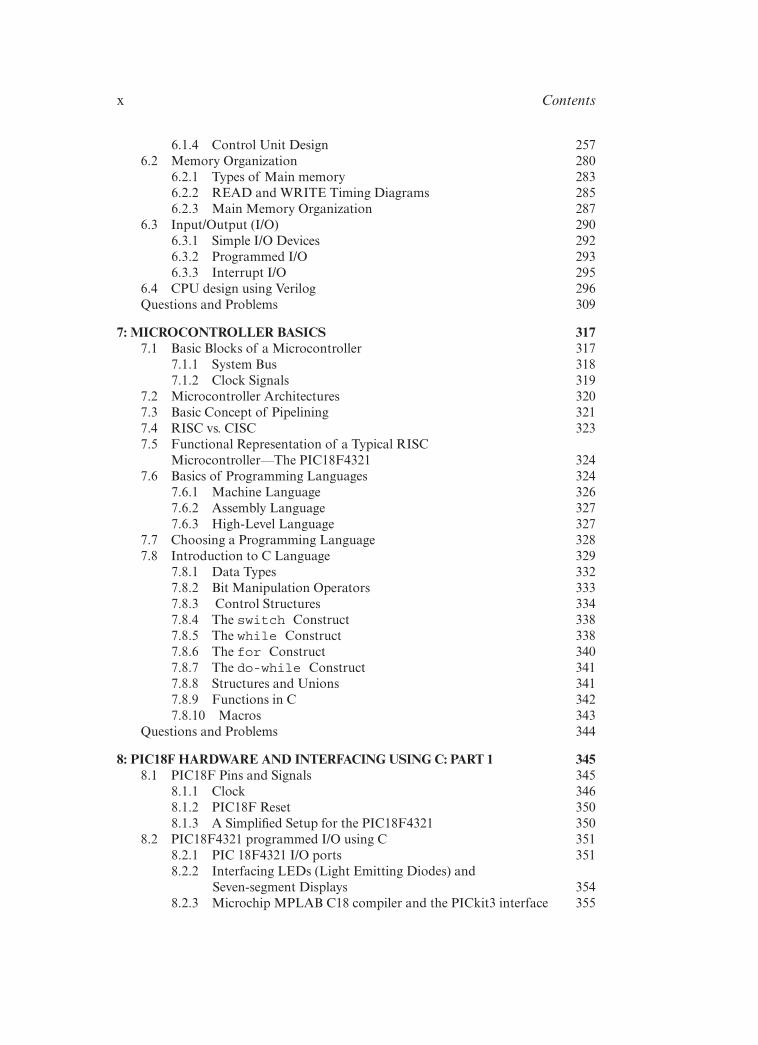
6.1.4 Control Unit Design 2576.2 Memory Organization 280
6.2.1 Types of Main memory 2836.2.2 READ and WRITE Timing Diagrams 2856.2.3 Main Memory Organization 287
6.3 Input/Output (I/O) 2906.3.1 Simple I/O Devices 2926.3.2 Programmed I/O 2936.3.3 Interrupt I/O 295
6.4 CPU design using Verilog 296Questions and Problems 309
7: MICROCONTROLLER BASICS 3177.1 Basic Blocks of a Microcontroller 317
7.1.1 System Bus 3187.1.2 Clock Signals 319
7.2 Microcontroller Architectures 3207.3 Basic Concept of Pipelining 3217.4 RISC vs. CISC 3237.5 Functional Representation of a Typical RISC
Microcontroller—The PIC18F4321 3247.6 Basics of Programming Languages 324
7.6.1 Machine Language 3267.6.2 Assembly Language 3277.6.3 High-Level Language 327
7.7 Choosing a Programming Language 3287.8 Introduction to C Language 329
7.8.1 Data Types 3327.8.2 Bit Manipulation Operators 3337.8.3 Control Structures 3347.8.4 The switch Construct 3387.8.5 The while Construct 3387.8.6 The for Construct 3407.8.7 The do-while Construct 3417.8.8 Structures and Unions 3417.8.9 Functions in C 3427.8.10 Macros 343
Questions and Problems 344
8: PIC18F HARDWARE AND INTERFACING USING C: PART 1 3458.1 PIC18F Pins and Signals 345
8.1.1 Clock 3468.1.2 PIC18F Reset 3508.1.3 A Simplified Setup for the PIC18F4321 350
8.2 PIC18F4321 programmed I/O using C 3518.2.1 PIC 18F4321 I/O ports 3518.2.2 Interfacing LEDs (Light Emitting Diodes) and
Seven-segment Displays 3548.2.3 Microchip MPLAB C18 compiler and the PICkit3 interface 355

Contents xi
8.2.4 Configuration commands 3568.3 PIC18F Interrupts 359
8.3.1 PIC18F Interrupt Types 3598.3.2 PIC18F External Interrupts in Default Mode 3598.3.3 Interrupt Registers and Priorities 3618.3.4 Setting the Triggering Levels of INTn Pin Interrupts 3628.3.5 Programming the PIC18 interrupts using C 363
Questions and Problems 369
9: PIC18F HARDWARE AND INTERFACING USING C: PART 2 3739.1 PIC18F Timers 373
9.1.1 Timer0 3759.1.2 Timer1 3789.1.3 Timer2 3829.1.4 Timer3 384
9.2 PIC18F Interface to an LCD (Liquid Crystal Display) 3909.3 Analog Interface 394
9.3.1 On-chip A/D Converter 3959.3.2 Interfacing an External D/A (Digital-to-Analog)
Converter to the PIC18F4321 4039.4 Serial Interface 405
9.4.1 Synchronous Serial Data Transmission 4059.4.2 Asynchronous Serial Data Transmission 4059.4.3 PIC18F Serial I/O 406
9.5 PIC18F4321 Capture/Compare/PWM (CCP) Modules 4139.5.1 CCP Registers 4139.5.2 CCP Modules and Associated Timers 4139.5.3 PIC18F4321 Capture Mode 4139.5.4 PIC18F4321 Compare Mode 4169.5.5 PIC18F4321 PWM (Pulse Width Modulation) Mode 417
9.6 DC Motor Control 419Questions and Problems 425
APPENDIX A: ANSWERS TO SELECTED PROBLEMS 429
APPENDIX B: GLOSSARY 439
APPENDIX C: TUTORIAL FOR COMPILING AND DEBUGGING A C-PROGRAM USING THE MPLAB 451
APPENDIX D: INTERFACING THE PIC18F4321 TO A PERSONAL COMPUTER OR A LAPTOP USING PICkit™ 3 479
D.1 INITIAL HARDWARE SETUP FOR THE PIC18F4321 479D.2 CONNECTING THE PERSONAL COMPUTER (PC) OR THE
LAPTOP TO THE PIC18F4321 VIA PICkit3 480D.3 PROGRAMMING THE PIC18F4321 FROM A PERSONAL
COMPUTER OR A LAPTOP USING THE PICkit3 482
BIBLIOGRAPHY 485
CREDITS 487
INDEX 489

xiii
PREFACE
The fifth edition of the book covered basics of computer engineering and science from digital logic to the design of a complete microcomputer system using Intel 8086 and Motorola 68000. With the growing popularity of microcontrollers, it is now necessary to have a clear understanding of the basic principles of microcontrollers at the undergraduate level. Microcontrollers play an important role in the design of digital systems. They are found in a wide range of applications including office automation systems such as copiers and fax machines, consumer electronics such as microwave ovens, digital instruments, and robotics.
Hence, a typical microcontroller such as Microchip Technology’s PIC18F is used to replace the 8086 and 68000 in this edition. Several PIC18F-based simple practical applications using C-language are provided. The sixth edition covers an enhanced version of both combinational and sequential logic design, basics of computer organization and microcontrollers.
Like the fifth edition, emphasis is given on the basic concepts. To cite an example, we clearly point out that computers understand only 0’s and 1’s. It is, therefore, important that students be familiar with binary numbers. Furthermore, we focus on the fact that computers can normally only add. Hence, all other arithmetic operations such as subtraction are performed via addition. This can be accomplished using two’s-complement arithmetic for binary numbers. This topic is, therefore, also included along with a clear explanation of signed and unsigned binary numbers. Basic concepts such as this are illustrated with simple examples throughout this edition.
As in the previous edition, three design levels are covered in this book: device level, logic level, and system level. Device-level design using simple devices such as transistors is included for typical logic gates such as NOT. Logic-level design is the technique in which logic gates are used; design of digital components such as an adder is provided. Finally, system-level applications are covered using a typical microcontroller such as the PIC18F.
Digital systems at the logic level are classified into two types of circuits: combinational and sequential. Combinational circuits have no memory whereas sequential circuits contain memory. Microcontrollers are designed using both combinational and sequential circuits. Therefore, these topics are covered in detail.
This edition of the book contains more details for synthesizing digital logic circuits using a popular hardware description language such as Verilog. An overview of contemporary digital circuit implementation using a popular programmable logic device (PLD) such as field programmable gate array (FPGA) along with the CAD (computer aided design) tools is included.
xiv Preface
Several chapters in the previous edition containing digital logic design have been retained and even strengthened in this edition. A few chapters of this new edition are written to present the fundamental concepts of C language programming and interfacing techniques associated with Microchip Technology’s PIC18F4321 microcontroller. The PIC18F family continues to be popular. The PIC18F family is an excellent educational tool for acquiring an understanding of both hardware and software aspects of typical microcontrollers.
Several PIC18F-based simple practical applications using C-language are provided. Most of the examples are implemented successfully in the laboratory. In summary, the sixth edition covers an enhanced version of both combinational and sequential logic, basics of computer organization, and microcontrollers.The following major changes have been provided in this edition:
Revised Chapters 1 through 5 of the fifth edition to update and strengthen certain topics on both combinational and sequential circuits. Several new examples are included. In addition, certain topics such as timing diagrams, hazards, stability, and Verilog and FPGA are enhanced.
Chapter 6 of this edition contains design of the CPU, memory, and I/O. Design of both hardwired and microprogrammed CPU is included.
Chapters 7 through 9 of this edition include microcontroller basics and PIC18F-based applications using C.
In this edition, the book is divided into nine chapters as follow:
Chapter 1 presents an explanation of basic terminologies, fundamental concepts of digital integrated circuits using transistors; a comparison of LSTTL, HC, and HCT IC characteristics, evolution of the microcontroller, and technological forecasts.
Chapter 2 includes various number systems and codes suitable for representing information in typical digital systems.
Chapter 3 covers Boolean algebra along with k-map simplification of Boolean functions. Several examples are included. The basic characteristics of digital logic gates are also presented.
Chapter 4 presents the analysis and design of combinational circuits. Typical combinational circuits such as adder, decoder, encoder, multiplexer, demultiplexer, and ROMs are included. An introduction to PLDs and FPGA is provided. Synthesis of combinational logic design using Verilog is also included.
Chapter 5 covers various types of flip-flops. Analysis and design of sequential circuits such as counters and registers are covered. An overview of topics such as flip-flop set-up time, hold time, and metastability is provided. Finally, synthesis of sequential logic design using Verilog is included.

Preface xv
Chapter 6 introduces basic concepts associated with CPU, memory, and I/O. It also covers the design of CPU including registers, ALU, and the control unit.
Chapter 7 presents basics of microcontroller including organization, memory, I/O, and C programming concepts.
Chapter 8 provides typical C programs which include I/O examples with LEDs and switches. PIC18F-based programmed and interrupt I/O using C are covered in a simplified manner.
Chapter 9 contains simple PIC18F-based applications using C. These include A/D and D/A converters, LCD displays, on-chip timers, DC voltmeter, and motor control using PWM (pulse width modulation).
The book can easily be adopted as a text for “digital logic design” and/or “introduction to microcontrollers” at the undergraduate level in electrical/computer engineering and computer science. The book introduces microcontroller hardware and software to form a bridge between digital logic and an advanced follow-up course in microcontrollers. The book provides an introduction to one of today’s popular microcontrollers, the PIC18F family. Although no advanced mathematical background is required, a basic course on DC circuits is required. A first course in C language programming is essential. Since C language programming is prerequisite for the course on microcontrollers, I/O and interfacing using C is included in this book. The audience for this book can also be practicing engineers and scientists in the industry. Practitioners of digital system design in the industry will find more simplified explanations, together with examples and comparison considerations, than are found in manufacturers’ manuals.
The author is especially indebted to his colleague, Dr. R. Chandra, of California State Polytechnic University, Pomona for reviewing the manuscript. The author is also grateful to his students Robert Benenyan, Michael Hachache, Cameron Chitsaz, Gagneet Bhatia, Luke Stankiewicz, and others for making constructive suggestions and to CJ Media of California for preparing the final version of the manuscript. Finally, the author is indebted to his deceased parents, who were primarily responsible for his accomplishments.
M. RAFIQUZZAMANPomona, California


1Fundamentals of Digital Logic and Microcontrollers, Sixth Edition. M. Rafiquzzaman.© 2014 John Wiley & Sons, Inc. Published 2014 by John Wiley & Sons, Inc.
1INTRODUCTION TO DIGITAL
SYSTEMSDigital systems are designed to store, process, and communicate information in digital form. They are found in a wide range of applications, including process control, communication systems, digital instruments, and consumer products. The digital computer, more commonly called the computer, is an example of a typical digital system.
A computer manipulates information in digital, or more precisely, binary form. A binary number has only two discrete values — zero or one. Each of these discrete values is represented by the OFF and ON status of an electronic switch called a transistor. All computers, therefore, only understand binary numbers. Any decimal number (base 10, with ten digits from 0 to 9) can be represented by a binary number (base 2, with digits 0 and 1).
The basic blocks of a computer are the central processing unit (CPU), the memory, and the input/output (I/O). The CPU of the computer is basically the same as the brain of a human. Computer memory is conceptually similar to human memory. A question asked to a human is analogous to entering a program into the computer using an input device such as the keyboard, and answering the question by the human is similar in concept to outputting the result required by the program to a computer output device such as the printer. The main difference is that human beings can think independently, whereas computers can only answer questions that they are programmed for. Computer hardware refers to components of a computer such as memory, CPU, transistors, nuts and bolts. Programs can perform a specific task such as addition if the computer has an electronic circuit capable of adding two numbers. Programmers cannot change these electronic circuits but can perform tasks on them using instructions.
Computer software, on the other hand, consists of a collection of programs. Programs contain instructions and data for performing a specific task. These programs, written using any programming language such as C, must be translated into binary prior to execution by the computer. This is because the computer only understands binary numbers. Therefore, a translator for converting such a program into binary is necessary. Hence, a translator program called the compiler is used for translating programs written in a programming language such as C into binary. These programs in binary form are then stored in the computer memory for execution because computers only understand 1’s and 0’s. Furthermore, computers can only add. This means that all operations such as subtraction, multiplication, and division are performed by addition.
Due to advances in semiconductor technology, it is possible to fabricate the CPU in a single chip. The result is the microprocessor. Both metal oxide semiconductor (MOS) and bipolar technologies were used in the fabrication process. The CPU can be placed on a single chip when MOS technology is used. However, several chips are

2 Fundamentals of Digital Logic and Microcontrollers
required with the bipolar technology. HCMOS (high speed complementary MOS) or BICMOS (combination of bipolar and HCMOS) technology (to be discussed later in this chapter) is normally used these days to fabricate the microprocessor in a single chip. Along with the microprocessor chip, appropriate memory and I/O chips can be used to design a microcomputer. The pins on each one of these chips can be connected to the proper lines on the system bus, which consists of address, data, and control lines. In the past, some manufacturers have designed a complete microcomputer on a single chip with limited capabilities. Single-chip microcomputers were used in a wide range of industrial and home applications.
“Microcontrollers” evolved from single-chip microcomputers. The micro-controllers are typically used for dedicated applications such as automotive systems, home appliances, and home entertainment systems. Typical microcontrollers, therefore, include a microcomputer, timers, and A/D (analog to digital) and D/A (digital to analog) converters — all in a single chip. Examples of typical microcontrollers are Intel 8751 (8-bit) / 8096 (16-bit) and Motorola/Freescale HC11 (8-bit) / HC16 (16-bit), and Microchip Technology PIC18F(8-bit)/PIC32(32-bit).
In this chapter, we first define some basic terms associated with the computers. We then describe briefly the evolution of the computers and the microcontrollers. Finally, a typical practical application, and technological forecasts are included.
1.1 Explanation of Terms
Before we go on, it is necessary to understand some basic terms (arranged in alphabetical order).
Address is a pattern of 0’s and 1’s that represents a specific location in memory or a particular I/O device. An 8-bit microcontroller with 16 address bits can produce 216 unique 16-bit patterns from 0000000000000000 to 1111111111111111, representing 65,536 different address combinations (addresses 0 to 65,535).
Addressing mode is the manner in which the microcontroller determines the operand (data) and destination addresses during execution of an instruction.
Arithmetic-logic unit (ALU) is a digital circuit that performs arithmetic and logic operations on two n-bit digital words. Typical operations performed by an ALU are addition, subtraction, ANDing, ORing, and comparison of two n-bit digital words. The size of the ALU defines the size of the microcontroller. For example, an 8-bit microcontroller contains an 8-bit ALU.
Big endian convention is used to store a 16-bit number such as 16-bit data in two bytes of memory locations as follows: the low memory address stores the high byte while the high memory address stores the low byte. The Motorola/Freescale HC11 8-bit microcontroller follows the big endian format.
Bit is an abbreviation for the term binary digit. A binary digit can have only two values, which are represented by the symbols 0 and 1, whereas a decimal digit can have 10 values, represented by the symbols 0 through 9. The bit values are easily implemented in electronic and magnetic media by two-state devices whose states portray either of the binary digits 0 and 1. Examples of such two-state devices are a transistor that is conducting or not conducting, a capacitor that is charged or discharged, and a magnetic material that is magnetized north to south or south to north.
Introduction to Digital Systems 3
Bit size refers to the number of bits that can be processed simultaneously by the basic arithmetic circuits of a microcontroller. A number of bits taken as a group in this manner is called a word. For example, an 8-bit microcontroller can process an 8-bit word. An 8-bit word is referred to as a byte, and a 4-bit word is known as a nibble.
Bus consists of a number of conductors (wires) grouped to provide a means of communication among different elements in a microcontroller system. The conductors in a bus can be grouped in terms of their functions. A microcontroller normally has an address bus, a data bus, and a control bus. Address bits are sent to memory or to an external device on the address bus. Instructions from memory, and data to/from memory or external devices, normally travel on the data bus.Control signals such as read/write for the other buses and among system elements are transmitted on the control bus. Buses are sometimes bidirectional; that is, information can be transmitted in either direction on the bus, but normally in only one direction at a time.
Clock is analogous to human heart beats. The microcontroller requires synchronization among its components, and this is provided by a clock or timing circuits.
The chip is an integrated circuit (IC) package containing digital circuits.
CPU (central processing unit) contains several registers (memory elements), an ALU, and a control unit. Note that the control unit translates instructions and performs the desired task. The number of peripheral devices depends on the particular application involved and may even vary within an application.
EEPROM or E2PROM (electrically erasable programmable ROM) is nonvolatile. EEPROMs can be programmed without removing the chip from the socket. EEPROMs are called read most memories (RMMs) because they have much slower write times than read times. Therefore, these memories are usually suited for applications when mostly reading rather than writing is performed. An example of EEPROM is the 2864 (8K x 8).
EPROM (erasable programmable ROM) is nonvolatile. EPROMs can be programmed and erased. The EPROM chip must be removed from the socket for programming. This memory is erased by exposing the chip to ultraviolet light via a lid or window on the chip. Typical erase times vary between 10 and 30 minutes. The EPROM is programmed by inserting the chip into a socket of the EPROM programmer, and providing proper addresses and voltage pulses at the appropriate pins of the chip. An example of EPROM is the 2764 (8K � 8).
Flash memory is designed using a combination of EPROM and EEPROM technologies. Flash memory is nonvolatile and is invented by Toshiba in mid 1980s. Flash memory can be programmed electrically while embedded on the board. One can change multiple bytes at a time. An example of flash memory is the Intel 28F020 (256K x 8). Flash memory is typically used in cell phones and digital cameras.
An FPGA (field programmable gate array) chip contains an array of digital logic blocks along with input and output blocks which can be connected together via programming using a hardware description language (HDL) such as Verilog or
4 Fundamentals of Digital Logic and Microcontrollers
VHDL. There are two types of components inside an FPGA. These are lookup table (stored in memory), and switch matrices. The concept of FPGA is based on the fact that a combinational circuit can be implemented using memory. In the past, digital logic circuits were built using all hardware (logic gates). It was a time-consuming task to debug the circuits. However, digital circuits implemented using FPGA’s are faster to debug since they are programmable. Note that it is much faster to debug software than hardware. Hence, products can be developed using FPGA from conceptual design via prototype to production in a very short time. Therefore, use of FPGA in digital logic is very common these days.
The term gate refers to digital circuits which perform logic operations such as AND, OR, and NOT. In an AND operation, the output of the AND gate is one if all inputs are one; the output is zero if one or more inputs are zero. The OR gate, on the other hand, provides a zero output if all inputs are zero; the output is one if one or more inputs are one. Finally, a NOT gate (also called an inverter) has one input and one output. The NOT gate produces one if the input is zero; the output is zero if the input is one.
Harvard architecture is a type of CPU architecture which uses separate instruction and data memory units along with separate buses for instructions and data. This means that these processors can execute instructions and access data simultaneously. Processors designed with this architecture require four buses for program memory and data memory. These are one data bus for instructions, one address bus for addresses of instructions, one data bus for data, and one address bus for addresses of data. The sizes of the address and data buses for instructions may be different from the address and data buses for data. Several microcontrollers including the PIC18F are designed using the Harvard architecture. This is because it is inexpensive to implement these buses inside the chip since both program and data memories are internal to the chip.
Instruction set of a microcontroller is a list of commands that the microcontroller is designed to execute. Typical instructions are ADD, SUBTRACT, and STORE. Individual instructions are coded as unique bit patterns which are recognized and executed by the microcontroller. If a microcontroller has three bits allocated to the representation of instructions, the microcontroller will recognize a maximum of 23, or eight, different instructions. The microcontroller will then have a maximum of eight instructions in its instruction set. It is obvious that some instructions will be more suitable than others to a particular application. For example, in a control application, instructions inputting digitized signals to the processor and outputting digital control variables to external circuits are essential. The number of instructions necessary in an application will directly influence the amount of hardware in the chip set and the number and organization of the interconnecting bus lines.
Little endian convention is used to store a 16-bit number such as 16-bit data in two bytes of memory locations as follows: the low memory address stores the low byte while the high memory address stores the high byte. The PIC18F microcontroller follows the little-endian format.
Microcomputer typically consists of a microprocessor (CPU) chip, input and output chips, and memory chips in which programs (instructions and data) are stored.
Introduction to Digital Systems 5
Microcontroller is implemented on a single chip containing a CPU, memory, and IOP (I/O and peripherals). Note that a typical IOP contains I/O unit of a microcomputer, timers, A/D (analog-to-digital) converter, analog comparators, serial I/O, and other peripheral functions (to be discussed later).
Microprocessor is the CPU of a microcomputer contained in a single chip, and must be interfaced with peripheral support chips in order to function.
Pipelining is a technique that overlaps instruction fetch (instruction read) with execution. This allows a microcontroller’s processing operation to be broken down into several steps (dictated by the number of pipeline levels or stages) so that the individual step outputs can be handled by the microcontroller in parallel. Pipelining is often used to fetch the microcontroller’s next instruction while executing the current instruction, which speeds up the overall operation of the microcontroller considerably. Microchip technology’s PIC18F (8-bit microcontroller) uses a two-stage instruction pipeline in order to speed up instruction execution.
Program contains instructions and data. Two conventions are used to store a 16-bit number such as 16-bit data in two bytes of memory locations. These are called little endian and big endian byte ordering. In little endian convention, the low memory address stores the low byte while the high memory address stores the high byte. For example, the 16-bit hexadecimal number, 2050 will be stored as two bytes in two 16-bit locations (Hex 5000 and Hex 5001) as follows: Address 5000 will contain 50 while address 5001 will store 20. In big endian convention, on the other hand, the low memory address stores the high byte while the high memory address stores the low byte. For example, the same 16-bit hexadecimal number, 2050 will be stored as two bytes in two 16-bit locations (Hex 5000 and Hex 5001) as follows: Address 5000 will contain 20 while address 5001 will store 50. Motorola / Freescale HC11 (8-bit microcontroller) follows big endian convention. Microchip PIC18F (8-bit microcontroller), on the other hand, follows the little endian format.
Random-access memory (RAM) is a storage medium for groups of bits or words whose contents cannot only be read but can also be altered at specific addresses. A RAM normally provides volatile storage, which means that its contents are lost in case power is turned off. There are two types of RAM: static RAM (SRAM) and dynamic RAM (DRAM). Static RAM stores data in flip-flops. Therefore, this memory does not need to be refreshed. An example of SRAM is 6116 (2K � 8). Dynamic RAM, on the other hand, stores data in capacitors. That is, it can hold data for a few milliseconds. Hence, dynamic RAMs are refreshed typically by using external refresh circuitry. Dynamic RAMs (DRAMs) are used in applications requiring large memory. DRAMs have higher densities than static RAMs (SRAMs). Typical examples of DRAMs are the 4464 (64K � 4), 44256 (256K � 4), and 41000 (1M � 1). DRAMs are inexpensive, occupy less space, and dissipate less power than SRAMs.
Read-only memory (ROM) is a storage medium for the groups of bits called words,and its contents cannot normally be altered once programmed. A typical ROM is fabricated on a chip and can store, for example, 2048 eight-bit words, which can be accessed individually by presenting to it one of 2048 addresses. This ROM is referred to as a 2K by 8-bit ROM. 10110111 is an example of an 8-bit word that might be stored in one location in this memory. A ROM is a nonvolatile storage
6 Fundamentals of Digital Logic and Microcontrollers
device, which means that its contents are retained in case power is turned off. Because of this characteristic, ROMs are used to store permanent programs (instructions and data).
Reduced Instruction Set Computer (RISC) contains a simple instruction set. In contrast, a Complex Instruction Set Computer (CISC) contains a large instruction set. The PIC18F is an RISC-based microcontroller while Motorola/Freescale HC11 is a CISC-based microcontroller.
Register can be considered as volatile storage for a number of bits. These bits may be entered into the register simultaneously (in parallel) or sequentially (serially) from right to left or from left to right, 1-bit at a time. An 8-bit register storing the bits 11110000 is represented as follows:
00001111
The speed power product (SPP) is a measure of performance of a logic gate. It is expressed in picojoules (pJ). SPP is obtained by multiplying the speed (ns) by the power dissipation (mW) of a gate.
Transistors are basically electronic switching devices. There are two types of transistors. These are bipolar junction transistors (BJTs) and metal-oxide semiconductor (MOS) transistors. The operation of the BJT depends on the flow of two types of carriers: electrons (n-channel) and holes (p-channel), whereas the MOS transistor is unipolar and its operation depends on the flow of only one type of carrier, either electrons (n-channel) or holes (p-channel).
von Neumann (Princeton) architecture uses a single memory unit and the same bus for accessing both instructions and data. Although CPUs designed using this architecture are slower compared to Harvard architecture since instructions and data cannot be accessed simultaneously because of the single bus, typical microprocessors such as the Pentium use this architecture. This is because memory units such as ROMs, EPROMs, and RAMs are external to the microprocessor. This will require almost half the number of wires on the mother board since address and data pins for only two buses rather than four buses (Harvard architecture) are required. This is the reason Harvard architecture would be very expensive if utilized in designing microprocessors. Note that microcontrollers using Harvard architecture internally will have to use von Neumann architecture externally. Texas Instrument’s MSP 430 uses the von Neumann architecture.
1.2 Design Levels
Three design levels can be defined for digital systems: systems level, logic level, and device level.
Systems level is the type of design in which CPU, memory, and I/O chips are interfaced to build a computer.
Logic level is the design technique in which chips containing logic gates such as AND, OR, and NOT are used to design a digital component such as the ALU.
Finally, device level utilizes transistors to design logic gates.

Introduction to Digital Systems 7
1.3 Combinational and Sequential Circuits
Digital circuits at the logic level can be classified into two types. These are combinationaland sequential.
Combinational circuits contain no memory, whereas sequential circuits require memory to remember the present state in order to go to the next state. A binary adder capable of providing the sum upon application of the numbers to be added is an example of a combinational circuit. For example, consider a 4-bit adder. The inputs to this adder will be two 4-bit numbers; the output will be the 4-bit sum. In this case, the adder will generate the 4-bit sum output upon application of the two 4-bit inputs.
Sequential circuits, on the other hand, require memory. The counter is an example of a sequential circuit. For instance, suppose that the counter is required to count in the sequence 0, 1, 2 and then repeat the sequence. In this case, the counter must have memory to remember the present count in order to go to the next. The counter must remember that it is at count 0 in order to go to the next count, 1. In order to count to 2, the counter must remember that it is counting 1 at the present state. In order to repeat the sequence, the counter must count back to 0 based on the present count, 2, and the process continues. A chip containing sequential circuit such as the counter will have a clock input pin.
In general, all computers contain both combinational and sequential circuits. However, most computers are regarded as clocked sequential systems. In these computers, almost all activities pertaining to instruction execution are synchronized with clocks.
1.4 Digital Integrated Circuits
The transistor can be considered as an electronic switch. The ON and OFF states of a transistor are used to represent binary digits. Transistors, therefore, play an important role in the design of digital systems. This section describes the basic characteristics of digital devices and logic families. These include diodes, transistors, and a summary of digital logic families. These topics are covered from a very basic point of view. This will allow the readers with some background in digital devices to see how they are utilized in designing digital systems.
1.4.1 Diodes
A diode is an electronic switch. It is a two-terminal device. Figure 1.1 shows the symbolic representation.
The positive terminal (made with the p-type semiconductor material) is called the anode; the negative terminal (made with the n-type semiconductor material) is called a cathode. When a voltage, V = 0.6 volt is applied across the anode and the cathode, the switch closes and a current I flows from anode to the cathode.
Anode Cathode
I
V+ +− −
FIGURE 1.1 Symbolic representations of a diode.

8 Fundamentals of Digital Logic and Microcontrollers
1.4.2 Transistors
A bipolar junction transistor (BJT) or commonly called the transistor is also an electronic switch like the diode. Both electrons (n-channel) and holes (p-channel) are used for carrier flow; hence, the name “bipolar” is used. The BJT is used in transistor logic circuits that have several advantages over diode logic circuits. First of all, the transistor acts as a logic device called an inverter. Note that an inverter provides a LOW output for a HIGH input and a HIGH output for a LOW input. Secondly, the transistor is a current amplifier (buffer). Transistors can, therefore, be used to amplify these currents to control external devices such as a light emitting diode (LED) requiring high currents. Finally, transistor logic gates operate faster than diode gates.
There are two types of transistors, namely npn and pnp. The classification depends on the fabrication process. npn transistors are widely used in digital circuits.
Figure 1.2 shows the symbolic representation of an npn transistor. The transistor is a three-terminal device. These are base, emitter, and collector. The transistor is a current-controlled switch. This means that an adequate current at the base will close the switch allowing a current to flow from the collector to the emitter.
This current direction is identified on the npn transistor symbol in Figure 1.2(a) by a downward arrow on the emitter. Note that a base resistance is normally required to generate the base current.
The transistor has three modes of operation: cutoff, saturation, and active. In digital circuits, a transistor is used as a switch, which is either ON (closed) or OFF (open). When no base current flows, the emitter-collector switch is open and the transistor operates in the cutoff (OFF) mode. On the other hand, when a base current flows such that the voltage across the base and the emitter is at least 0.6 V, the switch closes. If the base current is further increased, there will be a situation in which VCE
(voltage across the collector and the emitter) attains a constant value of approximately 0.2 V. This is called the saturation (ON) mode of the transistor. The “active” mode is between the cutoff and saturation modes. In this mode, the base current (IB) is amplified so that the collector current, IC = � IB, where � is called the gain, and is in the range of 10 to 100 for typical transistors. Note that when the transistor reaches saturation, increasing IB does not drop VCE below VCE (Sat.) of 0.2 V. On the other hand, VCE varies from 0.8 V to 5 V in the active mode. Therefore, the cutoff (OFF) and saturation (ON) modes of the transistor are used in designing digital circuits. The active mode of the transistor in which the transistor acts as a current amplifier (also called buffer) is used in digital output circuits.
Operation of the Transistor as an Inverter Figure 1.3 shows how to use the transistor as an inverter. When VIN = 0, the transistor is in cutoff (OFF), and the collector-emitter switch is open. This means that no current flows from +VCC to ground. VOUT is equal to +VCC. Thus, VOUT is high.
FIGURE 1.2 (a and b) Symbolic representations of an npn transistor.
Collector
Emitter
Base
IE
IB
IC
Base
Collector
Emitter
(a) npn )b(lobmysrotsisnarT Equivalent circuit

Introduction to Digital Systems 9
On the other hand, when VIN is HIGH, the emitter-collector switch is closed. A current flows from +VCC to ground. The transistor operates in saturation, and VOUT
= VCE (Sat) = 0.2 V ≈ 0. Thus, VOUT is basically connected to ground.Therefore, for VIN = LOW, VOUT = HIGH, and for VIN = HIGH, VOUT = LOW.
Hence, the npn transistor in Figure 1.3 acts as an inverter.Note that VCC is typically +5 V DC. The input voltage levels are normally
in the range of 0 to 0.8 volts for LOW and 2 volts to 5 volts for HIGH. The output voltage levels, on the other hand, are normally 0.2 volts for LOW and 3.6 volts for HIGH.
Light Emitting Diodes (LEDs) and Seven Segment Displays LEDs are extensively used as outputs in digital systems as status indicators. An LED is typically driven by low voltage and low current. This makes the LED a very attractive device for use with digital systems. Table 1.1 provides the current and voltage requirements of red, yellow, and green LEDs.
Basically, an LED will be ON, generating light, when its cathode is sufficiently negative with respect to its anode. A digital system such as a microcomputer can, therefore, light an LED either by grounding the cathode (if the anode is tied to +5 V) or by applying +5 V to the anode (if the cathode is grounded) through an appropriate resistor value. A typical hardware interface between a microcomputer and an LED is depicted in Figure 1.4. A microcomputer normally outputs 400 μA at a minimum
TABLE 1.1 Current and voltage requirements of LEDs
2.4V2.2V1.7 VVoltage20 mA10 mA10 mACurrent
GreenYellowRedLEDs
FIGURE 1.3 An inverter.
C
ER
+VCC
B
B
R C
VOUT
VINB
FIGURE 1.4 Microcomputer - LED interface.
R
+5 V
B
1
R 2
VM
LED (Red)
I μA
Microcomputer
= 400

10 Fundamentals of Digital Logic and Microcontrollers
voltage, VM = 2.4 volts for a HIGH. The red LED requires 10 mA at 1.7 volts. A buffer (current amplifier) such as a transistor is required to turn the LED ON. Since the transistor is an inverter, a HIGH input to the transistor will turn the LED ON. We now design the interface; that is, the values of R1, R2, and the gain � for the transistor will be determined. Note that the outputs of typical microcontrollers such as the PIC18F are buffered.
A HIGH at the microcomputer output will turn the transistor ON into active mode. This will allow a path of current to flow from the +5 V source through R2 and the LED to the ground. The appropriate value of R2 needs to be calculated to satisfy the voltage and current requirements of the LED. Also, suppose that VBE = 0.6 V when the transistor is in active mode. This means that R1 needs to be calculated with the specified values of VM = 2.4 V and I = 400 μA. The values of R1, R2, and � are calculated as follows:
R1 = VM − VBE
400 A = 2.4 − 0.6400 Aμ μ = 4.5 KΩ
Assuming VCE ý 0,
R2 = 5 − 1.7 − VCE
10 mA = 5 − 1.710 mA = 330
= IC
IB= 10 mA
400 A = 10 × 10−3
400 × 10−6 = 25μβ
Ω
Therefore, the interface design is complete, and a transistor with a minimum � of 25, R1 = 4.5 K�, and R2 = 330 � are required.
An inverting buffer chip such as the 74LS04 can be used in place of a transistor in Figure 1.4. A typical interface of an LED to a microcomputer via an inverter is shown in Figure 1.5. Note that the transistor base resistance is inside the inverter. Therefore, R1 is not required to be connected to the output of the microcomputer. The symbol is used to represent an inverter. Inverters will be discussed in more detail later. In Figure 1.5, when the microcomputer outputs a HIGH, the transistor switch inside the inverter closes. A current flows from the +5 V source, through the 330-ohm resistor and the LED, into the ground inside the inverter. The LED is thus turned ON.
Note that if 5V is used to turn the LED ON and 0V to turn it OFF, the LED should be connected as shown in Figure 1.6.
However, if 0 is used to to turn the LED ON and 5V to turn it OFF, the LED should be connected as shown in Figure 1.7.
Note that an LED must not be connected according to the circuit shown in Figure 1.8. This is because the circuit will not provide 1.7V accross the LED and a current of 10 ma through it.
+5 V
LED
Microcomputer
330 Ω
Inverter
FIGURE 1.5 Microcomputer - LED interface via an inverter.

Introduction to Digital Systems 11
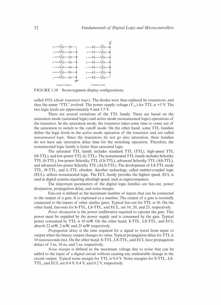
A seven-segment display can be used to display, for example, decimal numbers from 0 to 9. The name “seven segment” is based on the fact that there are seven LEDs — one in each segment of the display. Figure 1.9 shows a typical seven-segment display.
In Figure 1.9, each segment contains an LED. All decimal numbers from 0 to 9 can be displayed by turning the appropriate segment “ON” or “OFF”. For example, a zero can be displayed by turning the LED in segment g “OFF” and turning the other six LEDs in segments a through f “ON.” There are two types of seven-segment displays. These are common cathode and common anode. Figure 1.10 shows these display configurations.
In a common cathode arrangement, the microcomputer can send a HIGH to light a segment and a LOW to turn it off. In a common anode configuration, on the other hand, the microcomputer sends a LOW to light a segment and a HIGH to turn it off. In both configurations, R = 330 ohms can be used.
Transistor Transistor Logic (TTL) and Its Variations The transistor transistor logic (TTL) family of chips evolved from diodes and transistors. This family used to be
FIGURE 1.8 An invalid LED connection.
330 ohm
5 V+0V or
FIGURE 1.7 An LED connection to be turned ON by 5V and turned OFF by 5V.
5 V+0V
330 ohm
+ 5V
or
FIGURE 1.6 An LED connection to be turned ON by 5V and turned OFF by 0V.
5 V+or0V
330 ohm
FIGURE 1.9 A seven-segment display.
a
b
cd
e
fg
12 Fundamentals of Digital Logic and Microcontrollers
called DTL (diode transistor logic). The diodes were then replaced by transistors, and thus the name “TTL” evolved. The power supply voltage (VCC) for TTL is +5 V. The two logic levels are approximately 0 and 3.5 V.
There are several variations of the TTL family. These are based on the saturation mode (saturated logic) and active mode (nonsaturated logic) operations of the transistor. In the saturation mode, the transistor takes some time to come out of the saturation to switch to the cutoff mode. On the other hand, some TTL families define the logic levels in the active mode operation of the transistor and are called nonsaturated logic. Since the transistors do not go into saturation, these families do not have any saturation delay time for the switching operation. Therefore, the nonsaturated logic family is faster than saturated logic.
The saturated TTL family includes standard TTL (TTL), high-speed TTL (H-TTL), and low-power TTL (L-TTL). The nonsaturated TTL family includes Schottky TTL (S-TTL), low-power Schottky TTL (LS-TTL), advanced Schottky TTL (AS-TTL), and advanced low-power Schottky TTL (ALS-TTL). The development of LS-TTL made TTL, H-TTL, and L-TTL obsolete. Another technology, called emitter-coupled logic (ECL), utilizes nonsaturated logic. The ECL family provides the highest speed. ECL is used in digital systems requiring ultrahigh speed, such as supercomputers.
The important parameters of the digital logic families are fan-out, power dissipation, propagation delay, and noise margin.
Fan-out is defined as the maximum number of inputs that can be connected to the output of a gate. It is expressed as a number. The output of a gate is normally connected to the inputs of other similar gates. Typical fan-out for TTL is 10. On the other hand, fan-outs for S-TTL, LS-TTL, and ECL, are 10, 20, and 25, respectively.
Power dissipation is the power (milliwatts) required to operate the gate. This power must be supplied by the power supply and is consumed by the gate. Typical power consumed by TTL is 10 mW. On the other hand, S-TTL, LS-TTL, and ECL absorb 22 mW, 2 mW, and 25 mW respectively.
Propagation delay is the time required for a signal to travel from input to output when the binary output changes its value. Typical propagation delay for TTL is 10 nanoseconds (ns). On the other hand, S-TTL, LS-TTL, and ECL have propagation delays of 3 ns, 10 ns, and 2 ns, respectively.
Noise margin is defined as the maximum voltage due to noise that can be added to the input of a digital circuit without causing any undesirable change in the circuit output. Typical noise margin for TTL is 0.4 V. Noise margins for S-TTL, LS-TTL, and ECL are 0.4 V, 0.4 V, and 0.2 V, respectively.
FIGURE 1.10 Seven-segment display configurations.
+5 V
R
R
R
R
R
R
R
g
f
e
d
c
b
a
R
R
R
R
R
R
R
Common Cathode Common Anode
g
f
e
d
c
b
a
Related Documents