OVERVIEW Flash memory technology is a mix of EPROM and EEPROM technologies. The term flash was chosen because a large chunk of memory could be erased at one time. The name, therefore, dis- tinguishes flash devices from EEPROMs, where each byte is erased individually. Flash memory technology is today a mature technology. It is a strong competitor to other non- volatile memories such as EPROMs and EEPROMs, and to some DRAM applications. HOW THE DEVICE WORKS The more common elementary flash cell consists of one transistor with a floating gate, similar to an EPROM cell. However, technology and geometry differences between flash devices and EPROMs exist. In particular, the gate oxide between the silicon and the floating gate is thinner for flash technology. Source and drain diffusions are also different. These differences allow the flash device to be programmed and erased electrically. Figures 10- 1 and 10-2 show a comparison between a flash memory cell and an EPROM cell from a same manufac- turer (AMD) with the same technol- ogy complexity. The cells look similar since the gate oxide thick- ness and the source/drain diffusion differences are not visible in the photographs. INTEGRATED CIRCUIT ENGINEERING CORPORATION 10-1 10 FLASH MEMORY TECHNOLOGY Photos by ICE, “Memory 1997” 22482 POLY 2 WORD/SELECT POLY 1 FLOATING GATE N+ S/D N+ S/D ONO DIELECTRIC POLYCIDE OXIDE ON N+ N+ S/D ONO POLY 1 GATE OXIDE 1 EPROM MEMORY CELL FLASH MEMORY CELL Figure 10-1. AMD EPROM Versus AMD Flash Memory Cells

Welcome message from author
This document is posted to help you gain knowledge. Please leave a comment to let me know what you think about it! Share it to your friends and learn new things together.
Transcript
OVERVIEW
Flash memory technology is a mix of EPROM and EEPROM technologies. The term ÒflashÓ was
chosen because a large chunk of memory could be erased at one time. The name, therefore, dis-
tinguishes flash devices from EEPROMs, where each byte is erased individually.
Flash memory technology is today a mature technology. It is a strong competitor to other non-
volatile memories such as EPROMs and EEPROMs, and to some DRAM applications.
HOW THE DEVICE WORKS
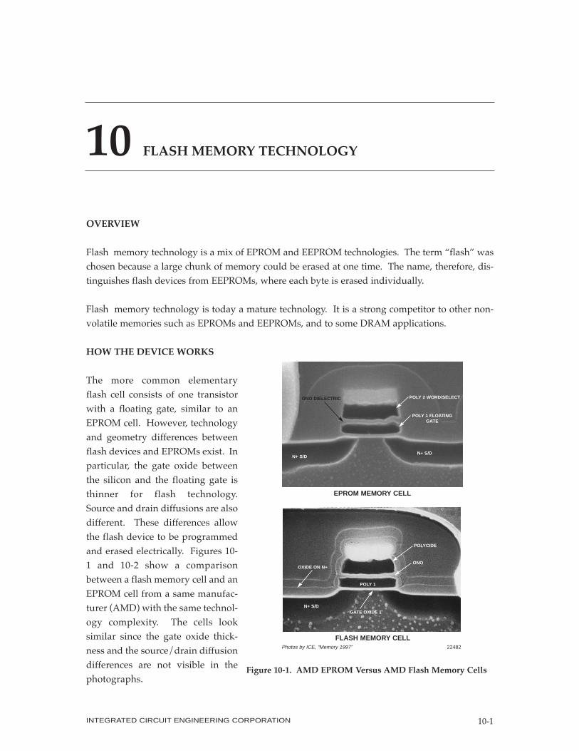
The more common elementary
flash cell consists of one transistor
with a floating gate, similar to an
EPROM cell. However, technology
and geometry differences between
flash devices and EPROMs exist. In
particular, the gate oxide between
the silicon and the floating gate is
thinner for flash technology.
Source and drain diffusions are also
different. These differences allow
the flash device to be programmed
and erased electrically. Figures 10-
1 and 10-2 show a comparison
between a flash memory cell and an
EPROM cell from a same manufac-
turer (AMD) with the same technol-
ogy complexity. The cells look
similar since the gate oxide thick-
ness and the source/drain diffusion
differences are not visible in the
photographs.
INTEGRATED CIRCUIT ENGINEERING CORPORATION 10-1
10 FLASH MEMORY TECHNOLOGY
Photos by ICE, “Memory 1997” 22482
POLY 2 WORD/SELECT
POLY 1 FLOATINGGATE
N+ S/DN+ S/D
ONO DIELECTRIC
POLYCIDE
OXIDE ON N+
N+ S/D
ONO
POLY 1
GATE OXIDE 1
EPROM MEMORY CELL
FLASH MEMORY CELL
Figure 10-1. AMD EPROM Versus AMD Flash Memory Cells
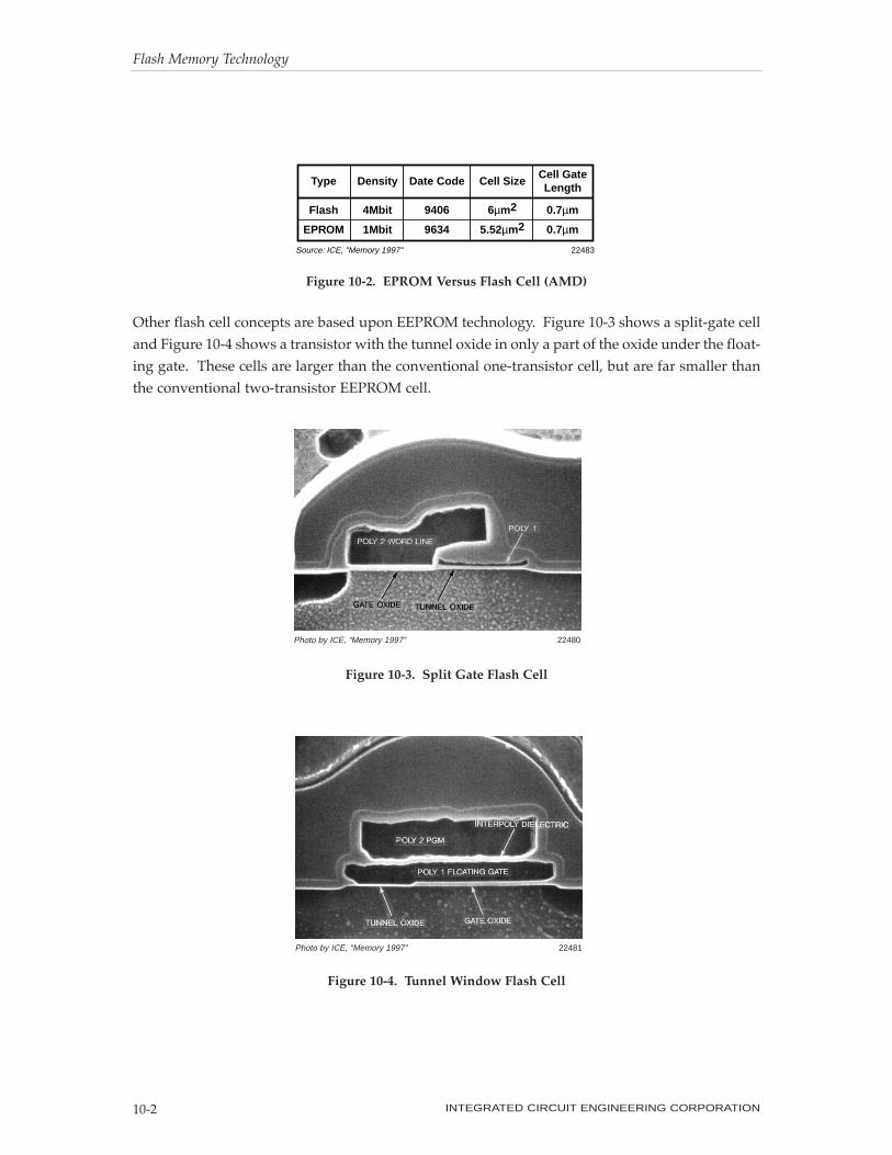
Other flash cell concepts are based upon EEPROM technology. Figure 10-3 shows a split-gate cell
and Figure 10-4 shows a transistor with the tunnel oxide in only a part of the oxide under the float-
ing gate. These cells are larger than the conventional one-transistor cell, but are far smaller than
the conventional two-transistor EEPROM cell.
Flash Memory Technology
INTEGRATED CIRCUIT ENGINEERING CORPORATION10-2
Figure 10-2. EPROM Versus Flash Cell (AMD)
Flash
EPROM
4Mbit
1Mbit
9406
9634
6µm2
5.52µm2
0.7µm
0.7µm
Type Density Date Code Cell SizeCell GateLength
Source: ICE, "Memory 1997" 22483
Photo by ICE, “Memory 1997” 22480
Figure 10-3. Split Gate Flash Cell
Figure 10-4. Tunnel Window Flash Cell
Photo by ICE, “Memory 1997” 22481
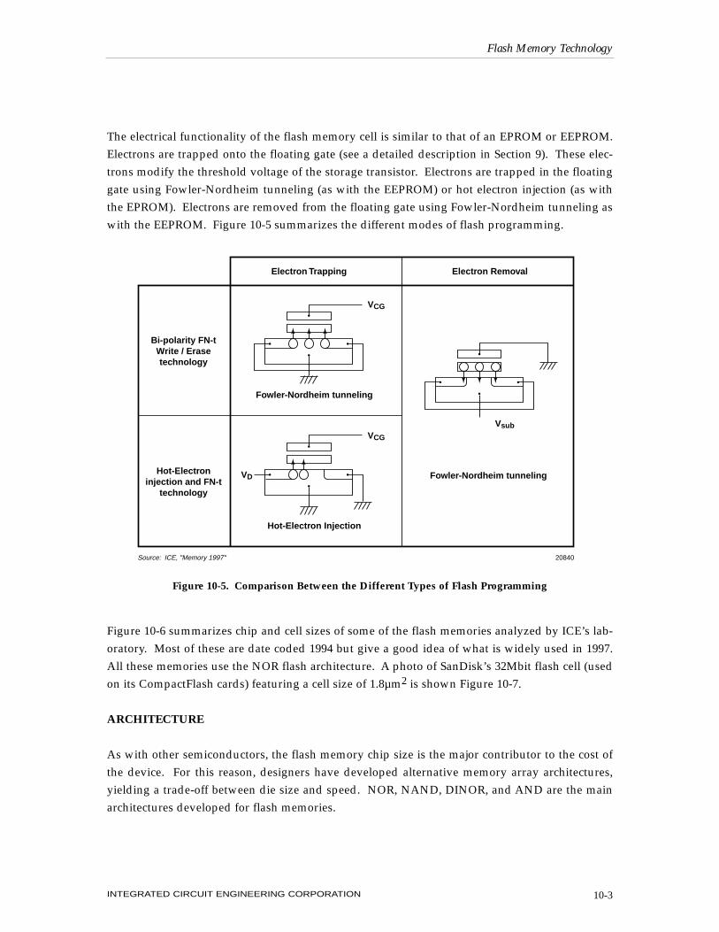
The electrical functionality of the flash memory cell is similar to that of an EPROM or EEPROM.Electrons are trapped onto the floating gate (see a detailed description in Section 9). These elec-trons modify the threshold voltage of the storage transistor. Electrons are trapped in the floatinggate using Fowler-Nordheim tunneling (as with the EEPROM) or hot electron injection (as withthe EPROM). Electrons are removed from the floating gate using Fowler-Nordheim tunneling aswith the EEPROM. Figure 10-5 summarizes the different modes of flash programming.
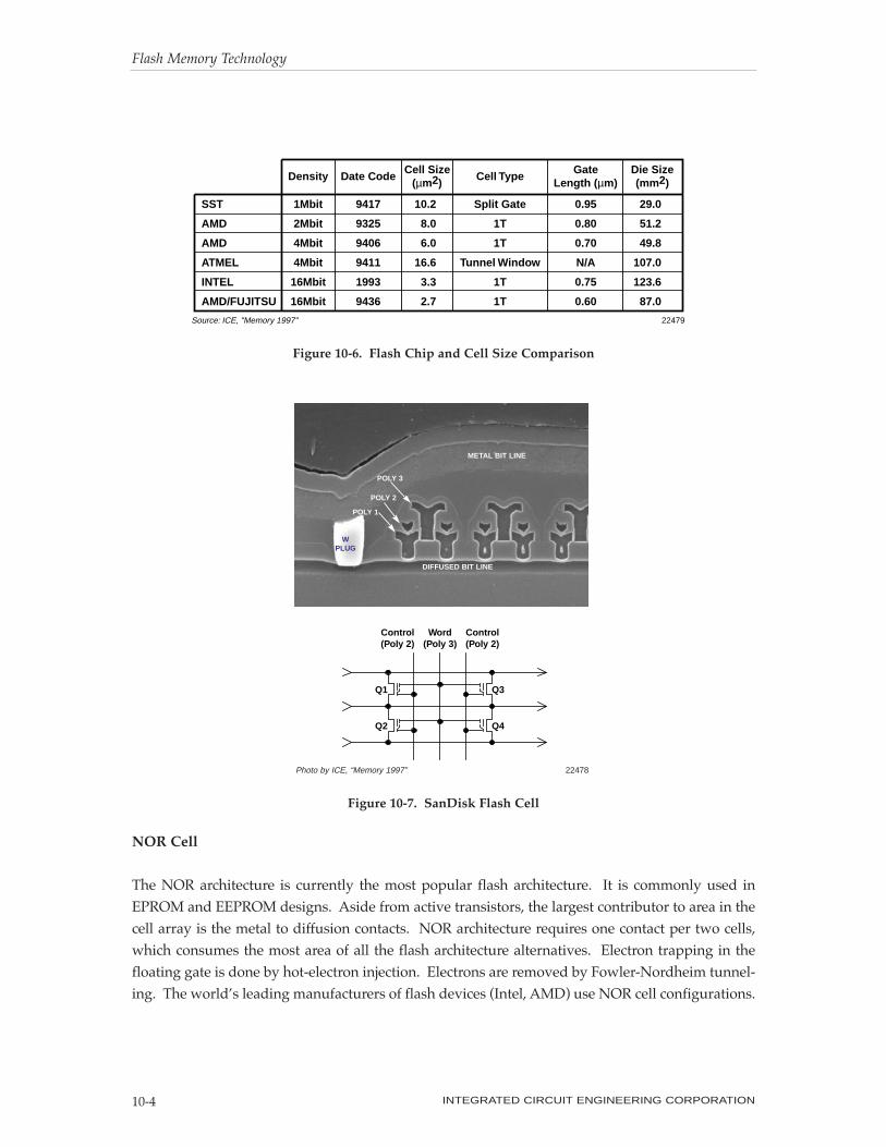
Figure 10-6 summarizes chip and cell sizes of some of the flash memories analyzed by ICE’s lab-oratory. Most of these are date coded 1994 but give a good idea of what is widely used in 1997.All these memories use the NOR flash architecture. A photo of SanDisk’s 32Mbit flash cell (usedon its CompactFlash cards) featuring a cell size of 1.8µm2 is shown Figure 10-7.
ARCHITECTURE
As with other semiconductors, the flash memory chip size is the major contributor to the cost ofthe device. For this reason, designers have developed alternative memory array architectures,yielding a trade-off between die size and speed. NOR, NAND, DINOR, and AND are the mainarchitectures developed for flash memories.
Flash Memory Technology
INTEGRATED CIRCUIT ENGINEERING CORPORATION 10-3
Bi-polarity FN-tWrite / Erasetechnology
Hot-Electroninjection and FN-t
technology
Fowler-Nordheim tunneling
Fowler-Nordheim tunneling
Hot-Electron Injection
VCG
VsubVCG
VD
Electron Trapping Electron Removal
Source: ICE, "Memory 1997" 20840
Figure 10-5. Comparison Between the Different Types of Flash Programming
NOR Cell
The NOR architecture is currently the most popular flash architecture. It is commonly used in
EPROM and EEPROM designs. Aside from active transistors, the largest contributor to area in the
cell array is the metal to diffusion contacts. NOR architecture requires one contact per two cells,
which consumes the most area of all the flash architecture alternatives. Electron trapping in the
floating gate is done by hot-electron injection. Electrons are removed by Fowler-Nordheim tunnel-
ing. The worldÕs leading manufacturers of flash devices (Intel, AMD) use NOR cell configurations.
Flash Memory Technology
INTEGRATED CIRCUIT ENGINEERING CORPORATION10-4
Photo by ICE, “Memory 1997” 22478
METAL BIT LINE
POLY 3
POLY 2
POLY 1
WPLUG
DIFFUSED BIT LINE
Q1
Control(Poly 2)
Word(Poly 3)
Control(Poly 2)
Q2
Q3
Q4
Figure 10-7. SanDisk Flash Cell
Figure 10-6. Flash Chip and Cell Size Comparison
SST
AMD
AMD
ATMEL
INTEL
AMD/FUJITSU
1Mbit
2Mbit
4Mbit
4Mbit
16Mbit
16Mbit
9417
9325
9406
9411
1993
9436
10.2
8.0
6.0
16.6
3.3
2.7
Split Gate
1T
1T
Tunnel Window
1T
1T
0.95
0.80
0.70
N/A
0.75
0.60
29.0
51.2
49.8
107.0
123.6
87.0
Density Date CodeCell Size
(µm2)Cell Type
GateLength (µm)
Die Size(mm2)
Source: ICE, "Memory 1997" 22479
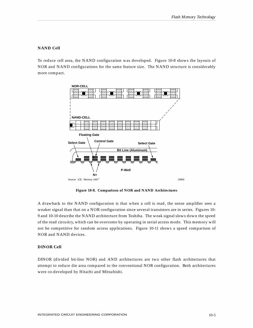
NAND Cell
To reduce cell area, the NAND configuration was developed. Figure 10-8 shows the layouts ofNOR and NAND configurations for the same feature size. The NAND structure is considerablymore compact.
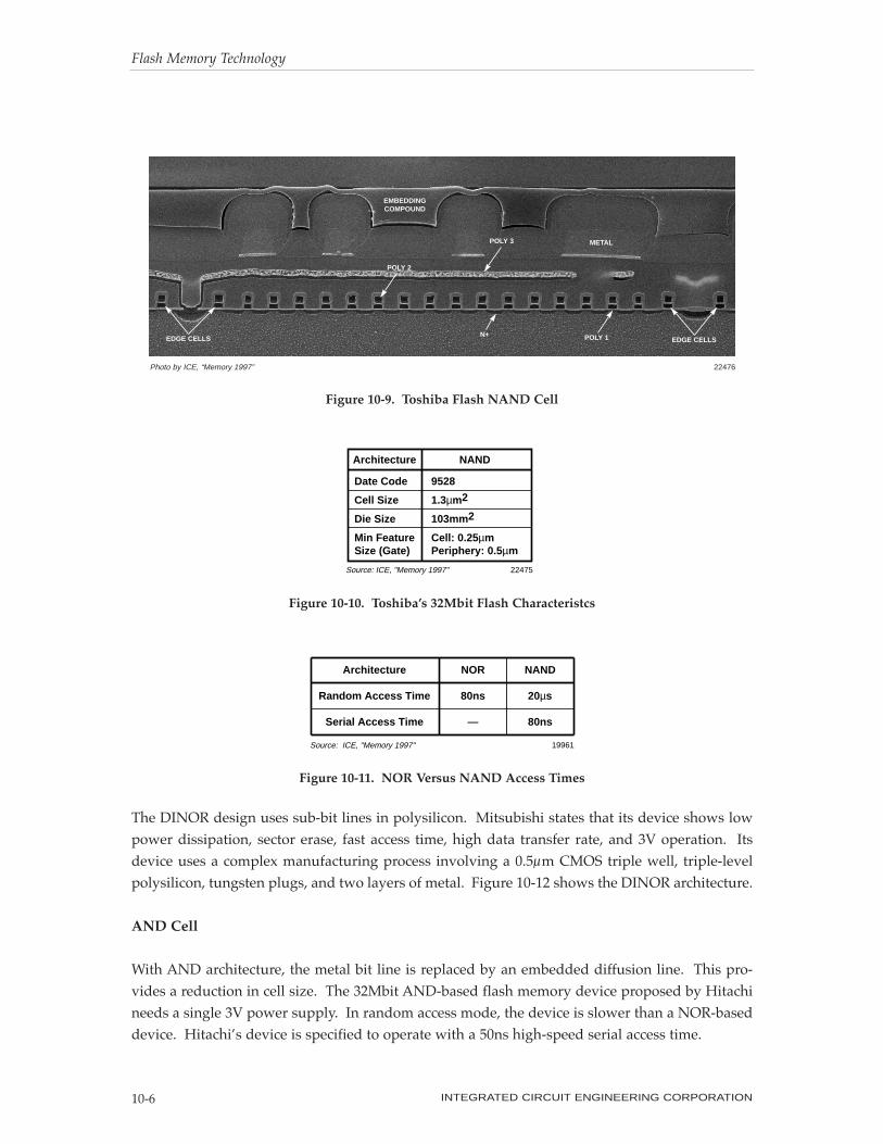
A drawback to the NAND configuration is that when a cell is read, the sense amplifier sees aweaker signal than that on a NOR configuration since several transistors are in series. Figures 10-9 and 10-10 describe the NAND architecture from Toshiba. The weak signal slows down the speedof the read circuitry, which can be overcome by operating in serial access mode. This memory willnot be competitive for random access applications. Figure 10-11 shows a speed comparison ofNOR and NAND devices.
DINOR Cell
DINOR (divided bit-line NOR) and AND architectures are two other flash architectures thatattempt to reduce die area compared to the conventional NOR configuration. Both architectureswere co-developed by Hitachi and Mitsubishi.
Flash Memory Technology
INTEGRATED CIRCUIT ENGINEERING CORPORATION 10-5
������������������������������������������������
Control Gate
Floating Gate
Select Gate
P-Well
N+
Select Gate
19960Source: ICE, "Memory 1997"
Bit Line (Aluminum)
��������
��������
������������
��������
������������
������������
��������
������������
������������
��������
������������
��������
������������
��������
��������
������������
NOR-CELL
NAND-CELL
Figure 10-8. Comparison of NOR and NAND Architectures
The DINOR design uses sub-bit lines in polysilicon. Mitsubishi states that its device shows low
power dissipation, sector erase, fast access time, high data transfer rate, and 3V operation. Its
device uses a complex manufacturing process involving a 0.5µm CMOS triple well, triple-level
polysilicon, tungsten plugs, and two layers of metal. Figure 10-12 shows the DINOR architecture.
AND Cell
With AND architecture, the metal bit line is replaced by an embedded diffusion line. This pro-
vides a reduction in cell size. The 32Mbit AND-based flash memory device proposed by Hitachi
needs a single 3V power supply. In random access mode, the device is slower than a NOR-based
device. HitachiÕs device is specified to operate with a 50ns high-speed serial access time.
Flash Memory Technology
INTEGRATED CIRCUIT ENGINEERING CORPORATION10-6
Photo by ICE, “Memory 1997” 22476
METALPOLY 3
POLY 2
EMBEDDINGCOMPOUND
EDGE CELLS POLY 1N+EDGE CELLS
Figure 10-9. Toshiba Flash NAND Cell
Figure 10-10. ToshibaÕs 32Mbit Flash Characteristcs
Figure 10-11. NOR Versus NAND Access Times
Date Code
Cell Size
Die Size
Min FeatureSize (Gate)
9528
1.3µm2
103mm2
Cell: 0.25µmPeriphery: 0.5µm
Architecture NAND
Source: ICE, "Memory 1997" 22475
Architecture
Random Access Time
Serial Access Time
NOR
80ns
—
NAND
20µs
80ns
19961Source: ICE, "Memory 1997"
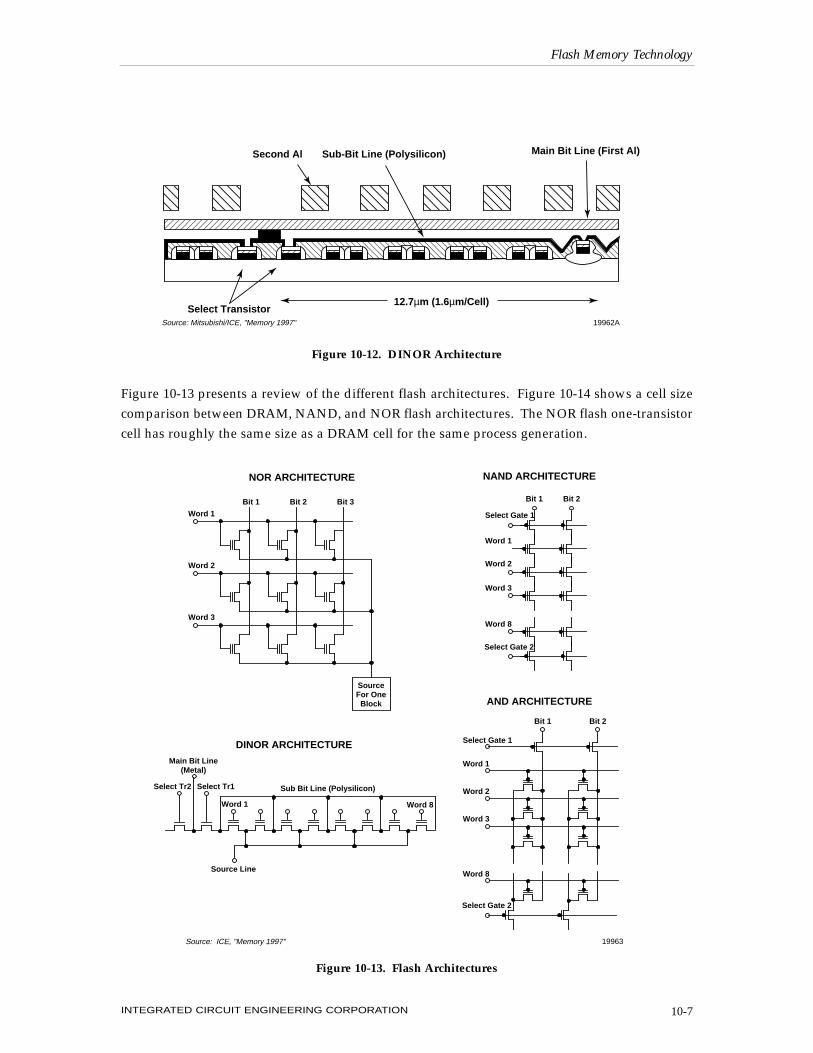
Figure 10-13 presents a review of the different flash architectures. Figure 10-14 shows a cell sizecomparison between DRAM, NAND, and NOR flash architectures. The NOR flash one-transistorcell has roughly the same size as a DRAM cell for the same process generation.
Flash Memory Technology
INTEGRATED CIRCUIT ENGINEERING CORPORATION 10-7
���������������������������������������������������������������������������������������������������������������������������
����������������������������������������������������
��������
������
������
��������
������
������
����
����
�������� ��
Select Transistor12.7µm (1.6µm/Cell)
Second Al Sub-Bit Line (Polysilicon) Main Bit Line (First Al)
19962ASource: Mitsubishi/ICE, "Memory 1997"
Figure 10-12. DINOR Architecture
Figure 10-13. Flash Architectures
SourceFor OneBlock
Word 3
Word 2
Word 1
Bit 1 Bit 2 Bit 3
19963Source: ICE, "Memory 1997"
Bit 1 Bit 2
Word 1
Word 2
Word 3
Word 8
Select Gate 2
Select Gate 1
Bit 1 Bit 2
Word 1
Word 2
Word 3
Word 8
Select Gate 2
Select Gate 1
Main Bit Line(Metal)
Word 1 Word 8
Sub Bit Line (Polysilicon)
Source Line
Select Tr2 Select Tr1
NOR ARCHITECTURE
DINOR ARCHITECTURE
AND ARCHITECTURE
NAND ARCHITECTURE
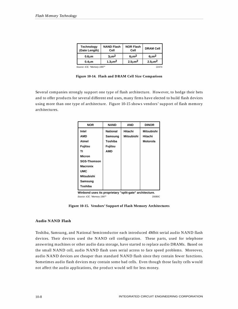
Several companies strongly support one type of flash architecture. However, to hedge their betsand to offer products for several different end uses, many firms have elected to build flash devicesusing more than one type of architecture. Figure 10-15 shows vendors’ support of flash memoryarchitectures.
Audio NAND Flash
Toshiba, Samsung, and National Semiconductor each introduced 4Mbit serial audio NAND flashdevices. Their devices used the NAND cell configuration. These parts, used for telephoneanswering machines or other audio data storage, have started to replace audio DRAMs. Based onthe small NAND cell, audio NAND flash uses serial access to face speed problems. Moreover,audio NAND devices are cheaper than standard NAND flash since they contain fewer functions.Sometimes audio flash devices may contain some bad cells. Even though those faulty cells wouldnot affect the audio applications, the product would sell for less money.
Flash Memory Technology
INTEGRATED CIRCUIT ENGINEERING CORPORATION10-8
Technology(Gate Length)
NAND FlashCell
NOR FlashCell
DRAM Cell
0.6µm
0.4µm
3µm2
1.3µm2
6µm2
2.5µm2
6µm2
2.5µm2
Source: ICE, "Memory 1997" 22474
Figure 10-14. Flash and DRAM Cell Size Comparison
Figure 10-15. Vendors’ Support of Flash Memory Architectures
NOR NAND AND DINOR
Intel
AMD
Atmel
Fujitsu
TI
Micron
SGS-Thomson
Macronix
UMC
Mitsubishi
Samsung
Toshiba
National
Samsung
Toshiba
Fujitsu
AMD
Hitachi
Mitsubishi
Mitsubishi
Hitachi
Motorola
20080C
Winbond uses its proprietary "split-gate" architecture.Source: ICE, "Memory 1997"
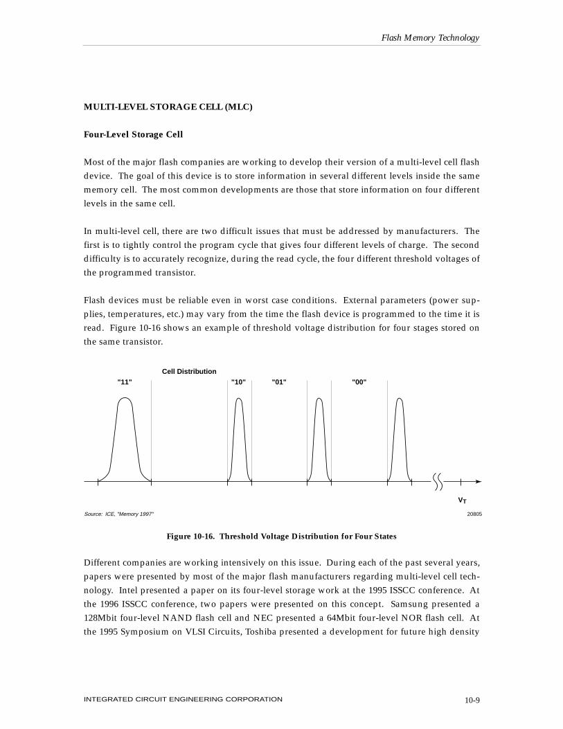
MULTI-LEVEL STORAGE CELL (MLC)
Four-Level Storage Cell
Most of the major flash companies are working to develop their version of a multi-level cell flashdevice. The goal of this device is to store information in several different levels inside the samememory cell. The most common developments are those that store information on four differentlevels in the same cell.
In multi-level cell, there are two difficult issues that must be addressed by manufacturers. Thefirst is to tightly control the program cycle that gives four different levels of charge. The seconddifficulty is to accurately recognize, during the read cycle, the four different threshold voltages ofthe programmed transistor.
Flash devices must be reliable even in worst case conditions. External parameters (power sup-plies, temperatures, etc.) may vary from the time the flash device is programmed to the time it isread. Figure 10-16 shows an example of threshold voltage distribution for four stages stored onthe same transistor.
Different companies are working intensively on this issue. During each of the past several years,papers were presented by most of the major flash manufacturers regarding multi-level cell tech-nology. Intel presented a paper on its four-level storage work at the 1995 ISSCC conference. Atthe 1996 ISSCC conference, two papers were presented on this concept. Samsung presented a128Mbit four-level NAND flash cell and NEC presented a 64Mbit four-level NOR flash cell. Atthe 1995 Symposium on VLSI Circuits, Toshiba presented a development for future high density
Flash Memory Technology
INTEGRATED CIRCUIT ENGINEERING CORPORATION 10-9
"10""11" "01" "00"
Cell Distribution
Source: ICE, "Memory 1997" 20805
VT
Figure 10-16. Threshold Voltage Distribution for Four States
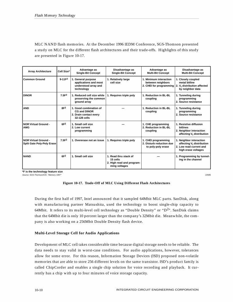
MLC NAND flash memories. At the December 1996 IEDM Conference, SGS-Thomson presenteda study on MLC for the different flash architectures and their trade-offs. Highlights of this studyare presented in Figure 10-17.
During the first half of 1997, Intel announced that it sampled 64Mbit MLC parts. SanDisk, alongwith manufacturing partner Matsushita, used the technology to boost single-chip capacity to64Mbit. It refers to its multi-level cell technology as “Double Density” or “D2”. SanDisk claimsthat the 64Mbit die is only 10 percent larger than the company’s 32Mbit die. Meanwhile, the com-pany is also working on a 256Mbit Double Density flash device.
Multi-Level Storage Cell for Audio Applications
Development of MLC cell takes considerable time because digital storage needs to be reliable. Thedata needs to stay valid in worst-case conditions. For audio applications, however, tolerancesallow for some error. For this reason, Information Storage Devices (ISD) proposed non-volatilememories that are able to store 256 different levels on the same transistor. ISD’s product family iscalled ChipCorder and enables a single chip solution for voice recording and playback. It cur-rently has a chip with up to four minutes of voice storage capacity.
Flash Memory Technology
INTEGRATED CIRCUIT ENGINEERING CORPORATION10-10
Array Architecture Cell Size*Advantage as
Single-Bit ConceptDisadvantage as
Single-Bit ConceptAdvantage as
Multi-Bit ConceptDisadvantage asMulti-Bit Concept
1. Closely coupledmetal bitline
2. Vt distribution affectedby neighbor data
1. Tunneling duringprogramming
2. Source resistance
1. Tunneling duringprogramming
2. Source resistance
1. Resistive diffusionbitlines
2. Neighbor interactionaffecting Vt distribution
1. Neighbor interactionaffecting Vt distribution
2. Low read current andhigh erase voltages
1. Programming by tunnel-ing in the channel
1. Minimum interactionbetween neighbors
2. CHEI for programming
1. Reduction in BL-BLcoupling
1. Reduction in BL-BLcoupling
1. CHE programming2. Reduction in BL-BL
coupling
1. CHEI programming2. Disturb reduction due
to poly-poly erase
—
1. Relatively largecell size
1. Requires triple poly
—
—
1. Requires triple poly
1. Read thru stack of15 cells
2. High read and program-ming voltages
1. General purposeapplications and mostunderstood array andtechnology
1. Reduced cell size whilepreserving the commonground array
1. Good combination ofCG and DINOR
2. Drain contact every32-128 cells
1. Small cell size2. Low current
programming
1. Overerase not an issue
1. Small cell size
9-11F2
7.5F2
8F2
6F2
7.5F2
6F2
Common Ground
DINOR
AND
NOR Virtual Ground -AMG
NOR Virtual Ground -Split Gate Poly-Poly Erase
NAND
*F is the technology feature sizeSource: SGS-Thomson/ICE, "Memory 1997" 22595
Figure 10-17. Trade-Off of MLC Using Different Flash Architectures
POWER SUPPLY
Currently, flash power supplies range from 5V/12V down to 2V. Flash memory power suppliesvary widely from vendor to vendor. There are two main reasons for this variation. First, flashcells need high voltage for programming. With different types of flash architectures and designs,different program/erase techniques (Fowler-Nordheim tunneling or hot-electron injection) exist.These architectures do not share the same voltage requirements. For example, high voltage withno current can be generated internally with a voltage pump. However the source/drain currentof hot-electron injection requires an external power supply.
The second reason for wide power supply variation is that there are many applications that cur-rently require different power supply levels. Some applications may require low-voltage flashdevices while others operate well using flash device with high-voltage characteristics.Manufacturers can propose different types of power supplies that best fit a specific application.
SmartVoltage
SmartVoltage is an Intel concept. However, other manufacturers including Sharp and Micronhave signed on to license the technology. SmartVoltage parts can be used for several power sup-plies. Read voltage may be 2.7V, 3.3V or 5.5V and programming voltage may be 3.3V, 5V or 12V.
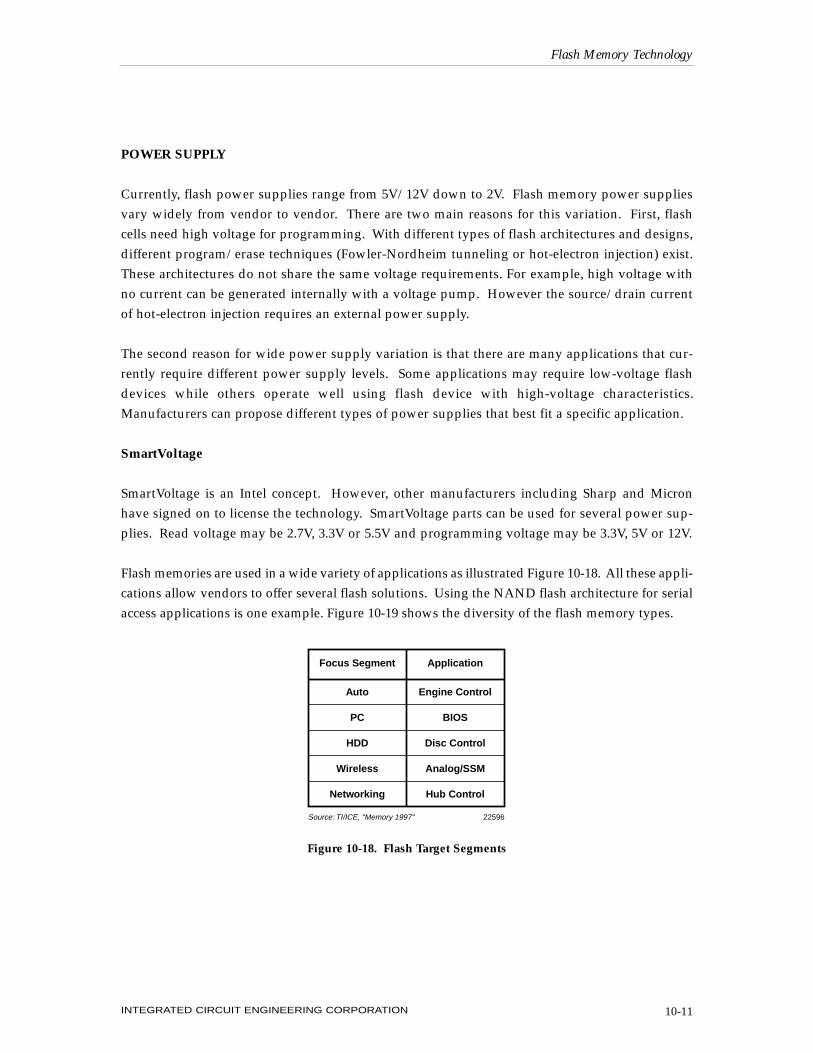
Flash memories are used in a wide variety of applications as illustrated Figure 10-18. All these appli-cations allow vendors to offer several flash solutions. Using the NAND flash architecture for serialaccess applications is one example. Figure 10-19 shows the diversity of the flash memory types.
Flash Memory Technology
INTEGRATED CIRCUIT ENGINEERING CORPORATION 10-11
22596Source: TI/ICE, "Memory 1997"
Focus Segment Application
Auto
PC
HDD
Wireless
Networking
Engine Control
BIOS
Disc Control
Analog/SSM
Hub Control
Figure 10-18. Flash Target Segments
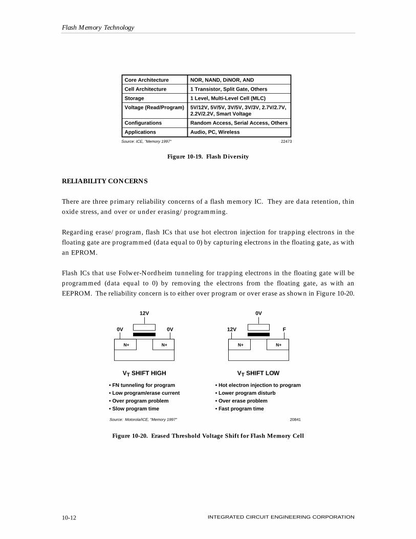
RELIABILITY CONCERNS
There are three primary reliability concerns of a flash memory IC. They are data retention, thinoxide stress, and over or under erasing/programming.
Regarding erase/program, flash ICs that use hot electron injection for trapping electrons in thefloating gate are programmed (data equal to 0) by capturing electrons in the floating gate, as withan EPROM.
Flash ICs that use Folwer-Nordheim tunneling for trapping electrons in the floating gate will beprogrammed (data equal to 0) by removing the electrons from the floating gate, as with anEEPROM. The reliability concern is to either over program or over erase as shown in Figure 10-20.
Flash Memory Technology
INTEGRATED CIRCUIT ENGINEERING CORPORATION10-12
Figure 10-19. Flash Diversity
Core Architecture
Cell Architecture
Storage
Voltage (Read/Program)
Configurations
Applications
NOR, NAND, DiNOR, AND
1 Transistor, Split Gate, Others
1 Level, Multi-Level Cell (MLC)
5V/12V, 5V/5V, 3V/5V, 3V/3V, 2.7V/2.7V,2.2V/2.2V, Smart Voltage
Random Access, Serial Access, Others
Audio, PC, Wireless
Source: ICE, "Memory 1997" 22473
N+ N+
F12V
0V
VT SHIFT LOW
0V 0V
12V
N+ N+
VT SHIFT HIGH
• FN tunneling for program
• Low program/erase current
• Over program problem
• Slow program time
• Hot electron injection to program
• Lower program disturb
• Over erase problem
• Fast program time
Source: Motorola/ICE, "Memory 1997" 20841
Figure 10-20. Erased Threshold Voltage Shift for Flash Memory Cell
PCMCIA
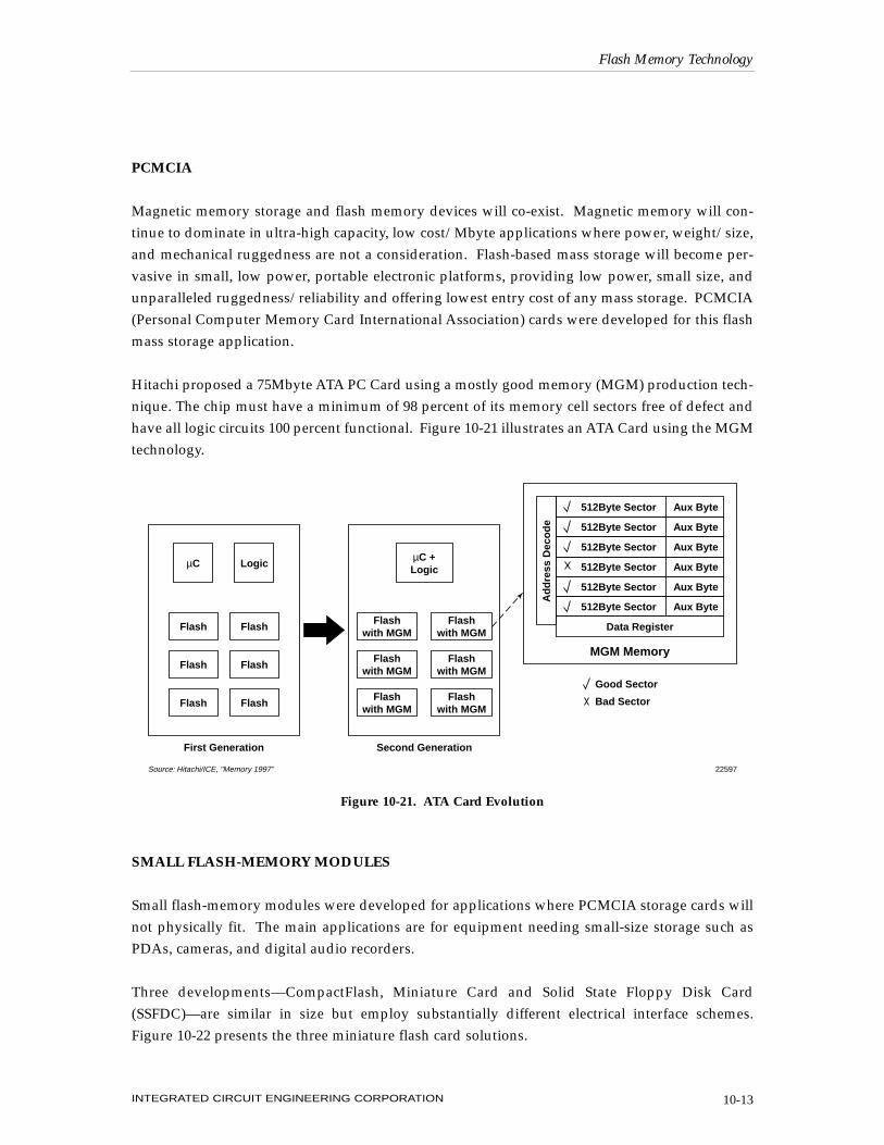
Magnetic memory storage and flash memory devices will co-exist. Magnetic memory will con-tinue to dominate in ultra-high capacity, low cost/Mbyte applications where power, weight/size,and mechanical ruggedness are not a consideration. Flash-based mass storage will become per-vasive in small, low power, portable electronic platforms, providing low power, small size, andunparalleled ruggedness/reliability and offering lowest entry cost of any mass storage. PCMCIA(Personal Computer Memory Card International Association) cards were developed for this flashmass storage application.
Hitachi proposed a 75Mbyte ATA PC Card using a mostly good memory (MGM) production tech-nique. The chip must have a minimum of 98 percent of its memory cell sectors free of defect andhave all logic circuits 100 percent functional. Figure 10-21 illustrates an ATA Card using the MGMtechnology.
SMALL FLASH-MEMORY MODULES
Small flash-memory modules were developed for applications where PCMCIA storage cards willnot physically fit. The main applications are for equipment needing small-size storage such asPDAs, cameras, and digital audio recorders.
Three developments—CompactFlash, Miniature Card and Solid State Floppy Disk Card(SSFDC)—are similar in size but employ substantially different electrical interface schemes.Figure 10-22 presents the three miniature flash card solutions.
Flash Memory Technology
INTEGRATED CIRCUIT ENGINEERING CORPORATION 10-13
Figure 10-21. ATA Card Evolution
µC +Logic
512Byte Sector Aux Byte
Data Register
MGM Memory
Ad
dre
ss D
eco
de
Good Sector
Bad Sector
Second GenerationFirst Generation
Source: Hitachi/ICE, "Memory 1997" 22597
Flashwith MGM
Flashwith MGM
Flashwith MGM
Flashwith MGM
Flashwith MGM
Flashwith MGM
µC Logic
Flash Flash
Flash Flash
Flash Flash
512Byte Sector Aux Byte
512Byte Sector Aux Byte
512Byte Sector Aux Byte
512Byte Sector Aux Byte
512Byte Sector Aux Byte
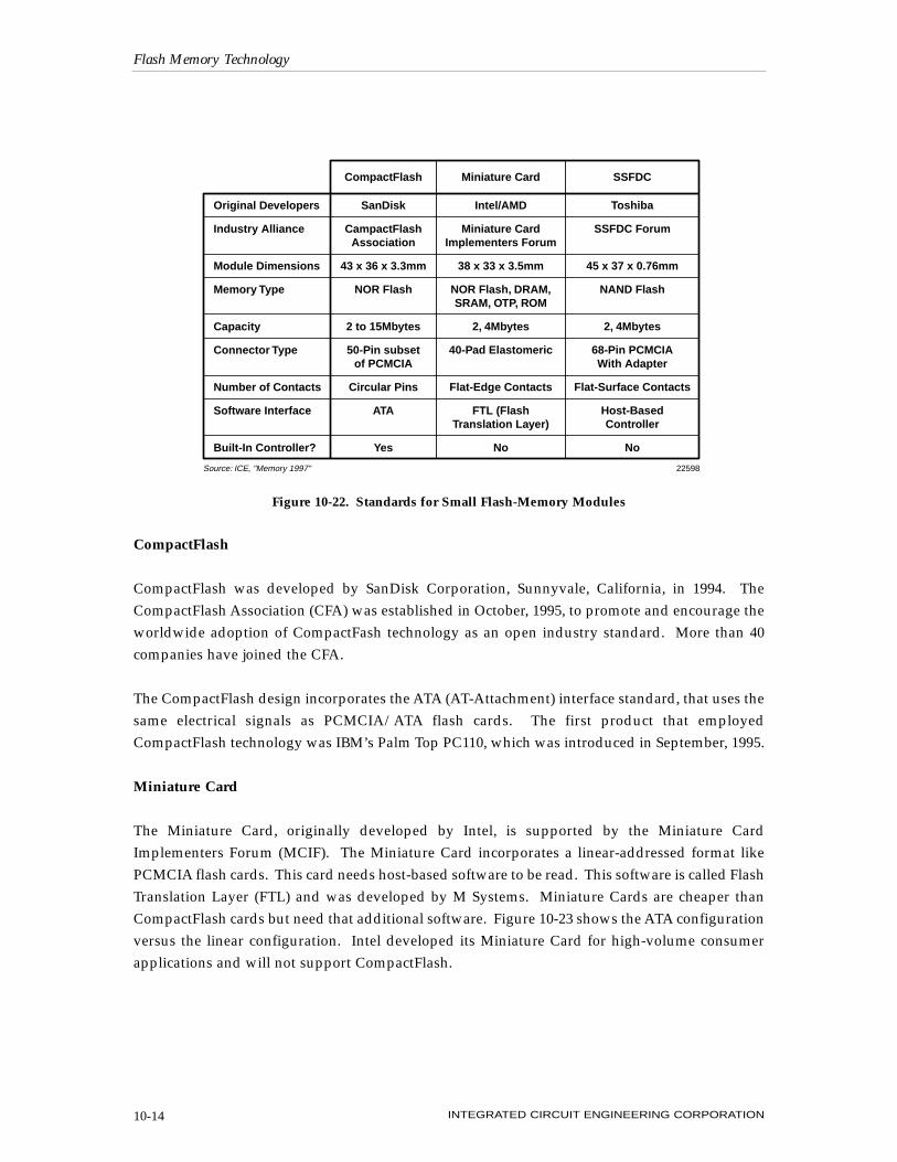
CompactFlash
CompactFlash was developed by SanDisk Corporation, Sunnyvale, California, in 1994. TheCompactFlash Association (CFA) was established in October, 1995, to promote and encourage theworldwide adoption of CompactFash technology as an open industry standard. More than 40companies have joined the CFA.
The CompactFlash design incorporates the ATA (AT-Attachment) interface standard, that uses thesame electrical signals as PCMCIA/ATA flash cards. The first product that employedCompactFlash technology was IBM’s Palm Top PC110, which was introduced in September, 1995.
Miniature Card
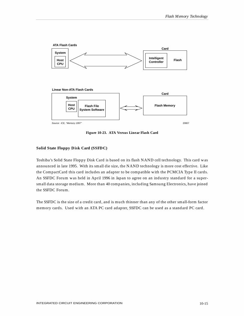
The Miniature Card, originally developed by Intel, is supported by the Miniature CardImplementers Forum (MCIF). The Miniature Card incorporates a linear-addressed format likePCMCIA flash cards. This card needs host-based software to be read. This software is called FlashTranslation Layer (FTL) and was developed by M Systems. Miniature Cards are cheaper thanCompactFlash cards but need that additional software. Figure 10-23 shows the ATA configurationversus the linear configuration. Intel developed its Miniature Card for high-volume consumerapplications and will not support CompactFlash.
Flash Memory Technology
INTEGRATED CIRCUIT ENGINEERING CORPORATION10-14
Original Developers
Industry Alliance
Module Dimensions
Memory Type
Capacity
Connector Type
Number of Contacts
Software Interface
Built-In Controller?
SanDisk
CampactFlashAssociation
43 x 36 x 3.3mm
NOR Flash
2 to 15Mbytes
50-Pin subsetof PCMCIA
Circular Pins
ATA
Yes
Intel/AMD
Miniature CardImplementers Forum
38 x 33 x 3.5mm
NOR Flash, DRAM,SRAM, OTP, ROM
2, 4Mbytes
40-Pad Elastomeric
Flat-Edge Contacts
FTL (FlashTranslation Layer)
No
Toshiba
SSFDC Forum
45 x 37 x 0.76mm
NAND Flash
2, 4Mbytes
68-Pin PCMCIAWith Adapter
Flat-Surface Contacts
Host-BasedController
No
CompactFlash Miniature Card SSFDC
Source: ICE, "Memory 1997" 22598
Figure 10-22. Standards for Small Flash-Memory Modules
Solid State Floppy Disk Card (SSFDC)
Toshiba’s Solid State Floppy Disk Card is based on its flash NAND cell technology. This card wasannounced in late 1995. With its small die size, the NAND technology is more cost effective. Likethe CompactCard this card includes an adapter to be compatible with the PCMCIA Type II cards.An SSFDC Forum was held in April 1996 in Japan to agree on an industry standard for a super-small data storage medium. More than 40 companies, including Samsung Electronics, have joinedthe SSFDC Forum.
The SSFDC is the size of a credit card, and is much thinner than any of the other small-form factormemory cards. Used with an ATA PC card adapter, SSFDC can be used as a standard PC card.
Flash Memory Technology
INTEGRATED CIRCUIT ENGINEERING CORPORATION 10-15
ATA Flash Cards
Linear Non-ATA Flash Cards
System
HostCPU
System
HostCPU
ATAIntelligentController
Flash
Card
Card
Flash FileSystem Software
Flash Memory
Source: ICE, "Memory 1997" 20807
Figure 10-23. ATA Versus Linear Flash Card
Flash Memory Technology
INTEGRATED CIRCUIT ENGINEERING CORPORATION10-16
Related Documents