1 LABORATORY: ELECTRONICS AND MODERN INSTRUMENTATION: Unit 1: Introduction to Basic Electronic Components. Test and Measurement Instruments Introduction In the designing of any electronic circuit, three mo st important considerations are: (i) Circuit components like resistors, Capacitors, Transistors and Diodes. (ii) Power sources like dc power supplies and signal generators (iii) Measurement and analysis instruments like multimeters and Cathode Ray Oscilloscope (CRO). This Unit deals with familiarization of basic components like resistors, Capacitors and diodes, followed by introduction to a few instruments like multimetrs and CRO. At the end a few experiments related with CRO have been explained. Basic Components: Basic components like capacitors, resistors, inductors, diodes, light emitting diode (led) and transistors can be divided into 2 categories: (i) Passive components like resistors and capacitors and (ii) Active components like diodes and transistors. The difference between the above two c ategories is that active components can gen erate energy whereas passive components can not generate energy. In other words active components can increase power of a signal whereas passive components often cause the power to be lost. Some components like resistors have their values marked on them whereas others like transistors do not have any value mar king but have a type number on them. One has to refer to datasheets to get to know the value of the unmarked component. Besides component values, they

Welcome message from author
This document is posted to help you gain knowledge. Please leave a comment to let me know what you think about it! Share it to your friends and learn new things together.
Transcript

7/28/2019 Experiment EDC
http://slidepdf.com/reader/full/experiment-edc 1/29
1
LABORATORY: ELECTRONICS AND MODERN INSTRUMENTATION:
Unit 1: Introduction to Basic Electronic Components. Test and
Measurement Instruments
Introduction
In the designing of any electronic circuit, three most important considerations are:
(i) Circuit components like resistors, Capacitors, Transistors and Diodes.
(ii) Power sources like dc power supplies and signal generators
(iii) Measurement and analysis instruments like multimeters and Cathode Ray
Oscilloscope (CRO).
This Unit deals with familiarization of basic components like resistors, Capacitors and diodes,
followed by introduction to a few instruments like multimetrs and CRO. At the end a few
experiments related with CRO have been explained.
Basic Components: Basic components like capacitors, resistors, inductors, diodes, light
emitting diode (led) and transistors can be divided into 2 categories: (i) Passive components like
resistors and capacitors and (ii) Active components like diodes and transistors. The difference
between the above two categories is that active components can generate energy whereas passive
components can not generate energy. In other words active components can increase power of a
signal whereas passive components often cause the power to be lost.
Some components like resistors have their values marked on them whereas others like
transistors do not have any value marking but have a type number on them. One has to refer to
datasheets to get to know the value of the unmarked component. Besides component values, they

7/28/2019 Experiment EDC
http://slidepdf.com/reader/full/experiment-edc 2/29
2
are also characterized by their ratings for e.g. maximum current value that a component can
stand without being burnt out.
Resistors: Resistors can be of two types: fixed value resistors or variable resistors. The
formula for resistance is given by: R = ρ l / A where ρ is resistivity, l is length and A is area of
crossection. Different value resistors can be manufactured by changing the length and area of
crossection or the material itself which changes the resistivity. Materials generally used for
fabrication of resistors are nichrome (80 % Ni and 20 % Cr), constatntan (55% cu and 45 % Ni
) and Manmganin (85 % Cu and 10 % Mn and < 5 % Ni). Metals are not used as they have a
very high temperature coefficient of resistance. Three main methods of fabrication are (i) a slab
or a rod of suitable resistivity, (ii) Material using thinner crossection and longer length. The
length is doubled and then wound in such a way that inductance effects are cancelled out. (iii)
Thin films of material on insulating substrate. Each resistor has a current carrying capacity.
Current more than the prescribed wattage may damage the resistor .
Colour Code for Resistors
Band colour
& its value
Band colour & its
tolerance
Black = 0
Brown = 1Red = 2
Orange = 3
Yellow = 4
Green = 5Blue = 6
Violet = 7
Grey = 8
White = 9
Gold = + - 5%
Silver = + - 10 % No colour means 20 %

7/28/2019 Experiment EDC
http://slidepdf.com/reader/full/experiment-edc 3/29
3
The first two bands near an end indicate first 2 digits, digit corresponding to 3rd
band is the
power of 10 to be multiplied and fourth band indicates tolerance as mentioned in the table. Refer
fig 1, where brown = 1, black = 0, red = 2 and silver = 10 % tolerance. Hence its value is
10 x 102 Ω = 1 k Ω.
Most commonly used resistors in lab are fixed value resistors which exist for standard values
according to E12. Other ranges are E24 and E48 Ranges.
E12 Range: Table 1 is for the values of resistors of E12 range. Topmost row defines the basic
value units of resistors in ohms. Every following row is 10 fold of the upper row.
Table 1: Table for E12 range values of resistors.
1.0 Ω 1.2 1.5 1.8 2.2 2.7 3.3 3.9 4.7 5.6 6.8 8.2 Ω
10 Ω 12 . . . . 68 82 Ω
100 Ω 680 820 Ω
1k 1.2k 6.8k 8.2k
10k 82k
100k 820k
1M 1.2M 6.8M` 8.2M
10M 12M 68M 82M
7/28/2019 Experiment EDC
http://slidepdf.com/reader/full/experiment-edc 4/29
4
Variable resistors Besides the fixed value resistors, there also exist variable resistors. The
resistance of variable resistors can vary in steps or continuously. Potentiometer is also an
example of continuously varying resistor
Special purpose resistors Light dependent resistors (LDR) and thermistors are examples of
special purpose resistors. Thermistor is a resistor whose value depends on its temperature. It is
also called a heat sensor. LDR is a resistance whose resistance depends upon the amount of
light falling on it.
Capacitors
Capacitors are capable of storing charges. They are used for coupling ac signals from one circuit
to another and for frequency selection etc. A capacitor consists of 2 metallic plates separated by
a dielectric. The capacitance is defined as : C = Єo Єr A / d, where A is the area of plates, d is
plates separation, Єo is permittivity of free space and Єr is relative permittivity. An important
parameter for capacitors is its voltage handling capacity beyond which the capacitor dielectric
breaks down.
The value of a capacitor depends upon the dielectric constant (K = Єo Єr .) of the material. There
are three main classes of capacitors: (i) Non electrolytic or normal capacitors and (ii) electrolytic
capacitors and (iii) variable capacitors. Normal capacitors are mostly of parallel plate type and
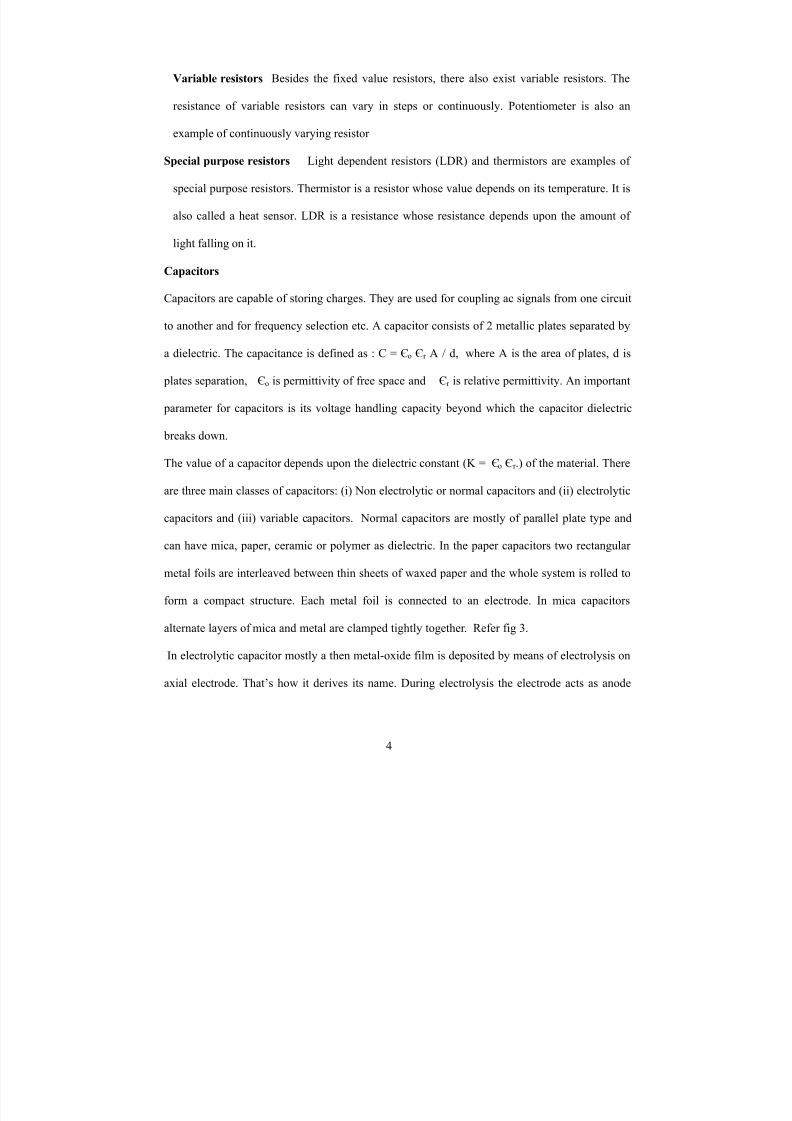
can have mica, paper, ceramic or polymer as dielectric. In the paper capacitors two rectangular
metal foils are interleaved between thin sheets of waxed paper and the whole system is rolled to
form a compact structure. Each metal foil is connected to an electrode. In mica capacitors
alternate layers of mica and metal are clamped tightly together. Refer fig 3.
In electrolytic capacitor mostly a then metal-oxide film is deposited by means of electrolysis on
axial electrode. That’s how it derives its name. During electrolysis the electrode acts as anode
7/28/2019 Experiment EDC
http://slidepdf.com/reader/full/experiment-edc 5/29
5
whose cathode is a concentric can. Since the dielectric layer is very thin hence these require
special precaution for their use: i.e. they have to connected in the right polarity failing which the
dielectric breaks down. Besides these fixed value capacitors we also have variable capacitors
whose value depends upon the area of crossection. They have a fixed set of plates and a movable
set of plates which can be moved through a shaft. This movement changes the area of overlap of
the two sets of plates which changes its capacity. Refer fig 3.
Colour and Number code of capacitors. Different marking schemes are used for electrolytic and
non-electrolytic capacitors. Temperature coefficient is of minor importance in an electrolytic
filter capacitor, but it is very important in ceramic trimmers for attenuator use. One never finds
temperature coefficient on an electrolytic label, but it is always present on ceramic trimmers.
(i) Electrolytic Capacitors: There are two designs of electrolytic capacitors: (i) Axial
where the leads are attached to each end (220µF in picture) and (ii) Radial where
both leads are at the same end (10µF in picture) Refer fig 4.

7/28/2019 Experiment EDC
http://slidepdf.com/reader/full/experiment-edc 6/29
6
(iii) Non-polarised capacitors ( < 1µF): Small value capacitors have their values printed but
without a multiplier. For example 0.1 means 0.1µF = 100nF. Sometimes the unit is placed in
between 2 digits indicating a decimal point. For example: 4n7 means 4.7nF.
Capacitor Number Code : A number code is often used on small capacitors where printing is
difficult: the 1st number is the 1st digit, the 2nd number is the 2nd digit, the 3rd number is the
power of ten to be multiplied., to give the capacitance in pF. Any letters just indicate tolerance
and voltage rating. For example: 102 means 10 X 102
pF = 1nF and 472J means 4700pF =
4.7nF (J means 5% tolerance).

7/28/2019 Experiment EDC
http://slidepdf.com/reader/full/experiment-edc 7/29
7
Capacitor Colour Code: Sometimes capacitors just show bands like resistors when printing
is tough on them. The colours should be read like the resistor code, the top three colour bands
giving the value in pF. The 4th band and 5th band are for tolerance and voltage rating
respectively. For example: brown, black, orange means 10000pF = 10nF = 0.01µF.
Available Values of Capacitors: Like resistors capacitors are also available for only
particular values. Following are 2 series defined for capacitors
The E3 series (3 values for each multiple of ten) 10, 22, 47, then it continues 1to100, 220, 470,
1000, 2200, 4700, 10000 etc.
The E6 series (6 values for each multiple of ten) 10, 15, 22, 33, 47, 68, ... then it continues 100,
150, 220, 330, 470, 680, 1000 etc.
Inductors: Inductor is a component made by a coil of wire which is wound on a core. It is
used to vary the impedance of a circuit or for frequency tuning. The value of an inductor depends
upon the total number of turns (N), area of crossection of the core (A) and length of the core
(l).The formula is L = μo μr N2
A / l. Its unit is in Henry.
Diode: A diode is a single junction device made of p and n type materials.. Its main function is to
rectify an ac signal although other special purpose diodes like zener and led’s are used for other

7/28/2019 Experiment EDC
http://slidepdf.com/reader/full/experiment-edc 8/29
8
purposes. A normal diode comes in a black casing whereas a zener diode has a transparent
casing. Their pictures and symbols are given in fig. 7.
Other diodes may be made by a p type and n type materials or between a semiconductor and a
metal. If the junction is made between a metal and semiconductor then it is called a Schottky
diode whose application is in rectifying and non-rectifying contacts and Schottky devices. If the
pn junction is made between very heavily doped materials then it forms a Zener diode. These are
used for voltage regulation in power supplies. and have breakdown voltages which are very low.
The normal diode has a breakdown voltage of greater than 100 V.
Some of the diode specifications are: Maximum reverse voltage (V br ), rated forward current (If ) ,
maximum forward voltage drop (Vf ) and package style. Table 3 gives some of the most
commonly used diodes with their specifications.
Table 3
Device
Number
Material
used.
IF (mA) VF(V) VBR
(V)
OA91 Ge 50 2.1 115

7/28/2019 Experiment EDC
http://slidepdf.com/reader/full/experiment-edc 9/29
9
In 4148 Si 100 1.0 75
In 4149 Si 100 1.0 75
IN 4007 Si 1000 1.6 1000
To test whether a given diode is O.K. or not, a simple multimter test can be performed which is
given later in this unit.
Light Emitting Diode (LED)
Led’sare pn junction devices which emit light radiation when biased in the forward direction.
The semiconductor material used for these junctions is a compound semiconductor like AlGaAs
whose band gap corresponds to a particular wavelength according to equation Eg = 1.24 / λ
where Eg is the band gap in ev and λ is the wavelength in microns. (e.g. red ~ 0.7 μ hence
corresponding E g = 1.24 / 0.7 = 1.77 ev). When the pn junction is forward biased, the electrons
are excited to conduction band and when they fall to the valence band, they give out energy in
the form of radiation corresponding to the Eg of the material Conventional led’s are made from
the materials like AlGaAs, GaAlP, GaAsP, GaP and GaN which emit Red, green, orange, yellow
and blue colours respectively. Led’s come in a special transparent casing as shown in fig 8..Dual
colour led’s are also available where two junctions are encapsulated on the same chip. It has
three leads where cathode is common whereas normal leds’ have two leads one for cathode and
other for anode. A very important precaution while using an led is the amount of current being
passed through it. For most leds the maximum allowable current is 20 mA beyond which the led
can burn out. Hence in most of the circuits a resistor is used to limit the current. Some important
specifications before using an led are: LED colour, peak wavelength, viewing angle, optical
power output, luminous intensity, forward current and forward voltage.

7/28/2019 Experiment EDC
http://slidepdf.com/reader/full/experiment-edc 10/29
10
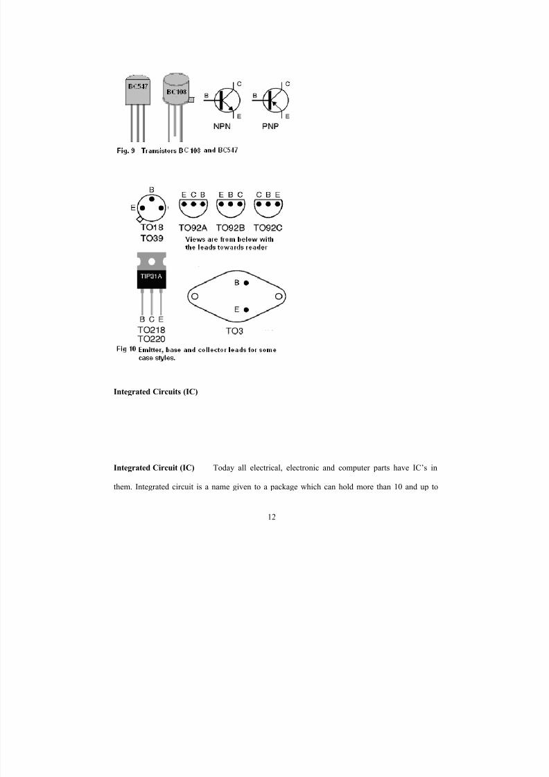
Transistors
Transistors are semiconductor devices used for applications like amplification of voltages,
current and are also used in oscillator circuits and switches. It’s a two junction and 3 terminal
device made of three layers of n and p type materials. The three regions are emitter, base and
collector. They are of 2 types (i) pnp and (ii) npn. Their most important specifications are Ic,
Vce, hfe and Power rating. They come in different casings like TO18, TO92C, and TO39 etc
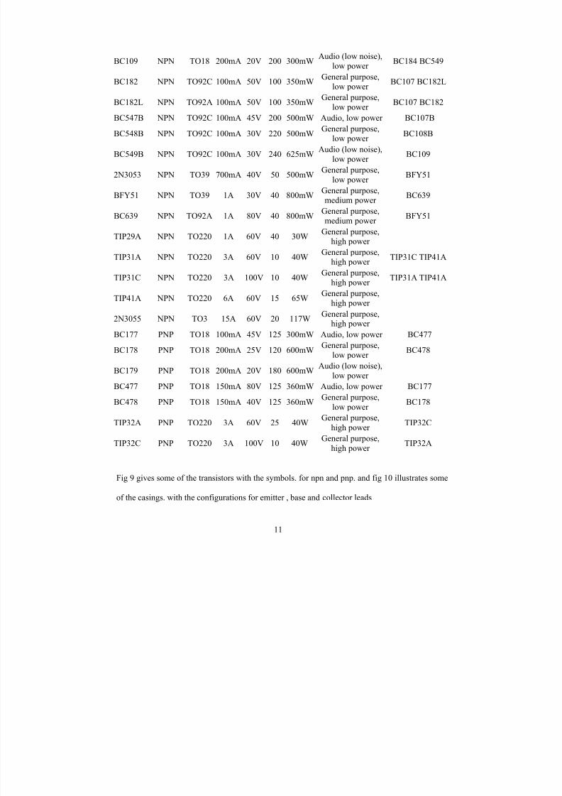
Given below is a table of most commonly used transistors with their specifications (approximate)
and casings. Datasheets from the companies can be referred to to know the exact specifications.
Code Structure Casestyle IC max. VCE max. hFE min. Ptot max. Category(typical use) Possiblesubstitutes
BC107 NPN TO18 100mA 45V 110 300mW Audio, low power BC182 BC547
BC108 NPN TO18 100mA 20V 110 300mWGeneral purpose,
low power BC108C BC183
BC548
BC108C NPN TO18 100mA 20V 420 600mWGeneral purpose,
low power
7/28/2019 Experiment EDC
http://slidepdf.com/reader/full/experiment-edc 11/29
11
BC109 NPN TO18 200mA 20V 200 300mWAudio (low noise),
low power BC184 BC549
BC182 NPN TO92C 100mA 50V 100 350mWGeneral purpose,
low power BC107 BC182L
BC182L NPN TO92A 100mA 50V 100 350mWGeneral purpose,
low power BC107 BC182
BC547B NPN TO92C 100mA 45V 200 500mW Audio, low power BC107B
BC548B NPN TO92C 100mA 30V 220 500mWGeneral purpose,
low power BC108B
BC549B NPN TO92C 100mA 30V 240 625mWAudio (low noise),
low power BC109
2N3053 NPN TO39 700mA 40V 50 500mWGeneral purpose,
low power BFY51
BFY51 NPN TO39 1A 30V 40 800mWGeneral purpose,medium power
BC639
BC639 NPN TO92A 1A 80V 40 800mWGeneral purpose,medium power BFY51
TIP29A NPN TO220 1A 60V 40 30WGeneral purpose,
high power
TIP31A NPN TO220 3A 60V 10 40WGeneral purpose,
high power TIP31C TIP41A
TIP31C NPN TO220 3A 100V 10 40WGeneral purpose,
high power TIP31A TIP41A
TIP41A NPN TO220 6A 60V 15 65WGeneral purpose,
high power
2N3055 NPN TO3 15A 60V 20 117WGeneral purpose,
high power BC177 PNP TO18 100mA 45V 125 300mW Audio, low power BC477
BC178 PNP TO18 200mA 25V 120 600mWGeneral purpose,
low power BC478
BC179 PNP TO18 200mA 20V 180 600mWAudio (low noise),
low power
BC477 PNP TO18 150mA 80V 125 360mW Audio, low power BC177
BC478 PNP TO18 150mA 40V 125 360mWGeneral purpose,
low power BC178
TIP32A PNP TO220 3A 60V 25 40WGeneral purpose,
high power
TIP32C
TIP32C PNP TO220 3A 100V 10 40WGeneral purpose,
high power TIP32A
Fig 9 gives some of the transistors with the symbols. for npn and pnp. and fig 10 illustrates some
of the casings. with the configurations for emitter , base and collector leads
7/28/2019 Experiment EDC
http://slidepdf.com/reader/full/experiment-edc 12/29
12
Integrated Circuits (IC)
Integrated Circuit (IC) Today all electrical, electronic and computer parts have IC’s in
them. Integrated circuit is a name given to a package which can hold more than 10 and up to

7/28/2019 Experiment EDC
http://slidepdf.com/reader/full/experiment-edc 13/29
13
millions of electronic components. They can give various functions like : (i) the function of a full
microprocessor circuit (eg 8085), (ii) a memory chip, (iii) a voltage regulator (LM 7805) or (iv)
Can contain just 10 AND gates (eg LS7400). They come in a black bench like casing with a
notch on one side and with electrical legs for connections, which are called pins. The size is
usually around 1 cm2
X 1 cm2. Refer to the picture. Its name is always written on top which
contains a few letters with numerals, according to its type, make and company. For example an
IC with name LS 7400 would mean LS series with And gates, LM741C - mA741C is an
operational amplifier (opamp). Datasheets can be referred to, to know the details of pin
configurations and make etc. The pins are usually read starting from left of notch and going
anticlockwise as shown in picture for 555 timer IC.
Fabrication of an IC is a highly sophisticated and expensive process requiring clean rooms and
very expensive equipments like photolithography, metallization and diffusion etc. But because of
their bulk manufacture and requirement the cost of each IC is very low.
Instruments:

7/28/2019 Experiment EDC
http://slidepdf.com/reader/full/experiment-edc 14/29
14
Multimeters: A multimeter is an instrument which measures electrical parameters such as AC or
DC voltage, current, and resistance. Rather than having separate meters, a multimeter combines a
voltmeter, an ammeter, and an ohmmeter. The two main kinds of a multimeter are analog and
digital. Refer fig 10. A digital multimeter has an LCD screen that displays the value of the
parameter being measured. while in an analog multimeter display, a needle moves through a
graduated scale. Topmost scale is usually for resistance and the readings increases from right to
left while other scales readings increase from left to right. Another name for an analog
multimeter is Volt-Ohm-Milliammeter (VOM). Each type of meter has its advantages and
disadvantaged. When used as a voltmeter, a digital meter is usually better because its resistance
is much higher, 1 M or 10 M, compared to 200 Ω for an analogue multimeter for a similar range.
On the other hand, it is easier to follow a slowly changing voltage by watching the needle on an
analogue display. Most modern multimeters are digital and traditional analogue types are
becoming obsolete

7/28/2019 Experiment EDC
http://slidepdf.com/reader/full/experiment-edc 15/29
15
Block diagram of a VOM is given in fig. 11
Voltage measurement by multimeter: For the case of a VOM, a zero adjustment has to be
made every time the multimeter is to be used. To do the zero adjustment, set the mode selection
knob in resistance mode. Connect the two leads to positive and common terminals respectively
and short the leads. The needle should move to extreme right to the last reading on the ohms
scale. If it stops before or goes beyond then the zero adjustment knob has to be rotated
(clockwise or anticlockwise) such that the needle rests at the last reading on the right end of the
bar on the ohms scale. Subsequently, to measure voltage, the multimeter has to be first set in AC
or DC mode. After selecting a suitable range defined by the uppermost limit of the expected
value, the range knob has to be set. Next connect the common (gnd) terminal through a lead
(black) to the gnd of the circuit and the red lead to the point where voltage is to be measured. For
7/28/2019 Experiment EDC
http://slidepdf.com/reader/full/experiment-edc 16/29
16
the case of an analogue multimeter, if the needle goes the wrong way the leads have to be
reversed or if the needle doesn’t move at all the range has to be changed. To find the value of
the voltage, read the number from that scale that matches the range being used. In a digital
multimeter, if 1. is displayed then the range has to be increased..
Resistance Measurement: To measure resistance in a circuit, first the power supply is to be
turned off (or disconnected) otherwise the multimeter might get damaged. Next, select a range on
the multimeter and touch two metal points in the circuit. If the needle doesn’t move or goes all
the way to the end of the scale, select another range. One can not use this method to measure the
resistance of a resistor in the circuit because there may be other paths between the nodes of a
resistor. One leg of a resistor must be disconnected from the circuit to make sure that the only
path between the two probes is through that resistor. To measure the resistance of a resistor,
select the range on the meter that might be closest to the right value and use the probes to touch
either side of the resistor. If the right range is selected then the needle will be somewhere
between the left and the right end of the scale. To find the value of the resistor, read the number
from the scale that matches the range you are using.
MULTIMETER TEST OF DIODES
One can know whether a specific terminal of a diode is n or p by measuring the resistance with
multimeter. To do so keep the multimeters in resistance mode connect its positive lead to the
anode of diode and negative lead to its cathode. During the test, the multimeter passes current
through the diode and the diode gets forward biased. It thus indicated very low resistance of the
order of 100 . If the leads are now reversed than the diode gets reverse biased and offers very
high resistance of the order of M. This can be read in the multimeter again. If a diode reads

7/28/2019 Experiment EDC
http://slidepdf.com/reader/full/experiment-edc 17/29
17
very low resistance in the forward as well as reverse bias then it is shorted. On the other hand if
it reads high resistance in the forward as well as reverse bias then it is open.
FUNCTION GENERATORS
Function Generators are instruments capable of generating an ac signal of any frequency (~
100Hz – hundreds of kHz), voltage(~1 mv – 20V) and various forms (e.g. sine wave, Square
pulse, Saw tooth wave, Triangular wave or noise waveform). They also provide a continuously
variable dc offset, variable duty cycle. They are usually of 2 types: (i) analog and (ii) Digital.
Some of the front panel controls of a typical function generator are:
1 Power Switch For switching obn the power supply

7/28/2019 Experiment EDC
http://slidepdf.com/reader/full/experiment-edc 18/29
18
2 Digital Display This is a 4 digit frequency meter
3 OFFSET This knob is for adding a dc voltage to the output signal
4 Amplitude This does the continuous adjustment of output voltage
5 Speed This is for setting wobulation speed
6 Width This knob is for setting the wobulation width
7 Frquency This knob is for selecting the frequency range from 0.3 Hz to 3MHz in
decade steps.
8. Sweep On This is a push button for activating internal sweep
9 Mode Selection Push Button for triangular, sine Square etc.
10 BNC connector This is a 50 Ω output BNC connector
11 -20 db, - 20 db A push button control for -20 db attenuation. When both buttons are
pushed then a total of 40 db attenuation is got.
Cathode Ray Oscilloscope (CRO)
CRO is an instrument which is used to measure voltages that change with time and to display the
waveforms in real time mode. There is a graphical scale present on the screen which is used to
calculate the voltage or frequency value. A very important specification of a CRO is its

7/28/2019 Experiment EDC
http://slidepdf.com/reader/full/experiment-edc 19/29
19
bandwidth which gives the maximum frequency of a signal which a CRO can measure. A simple
oscilloscope consists of a cathode ray tube, a vertical amplifier, a time base, a horizontal
amplifier and a power supply. Fig 12 shows the block diagram of a CRO. Cathode-ray tube is a
vacuum tube in which a beam of electrons is produced and focused onto a fluorescent screen.
The electrons’ kinetic energy is converted into light energy as they collide with the screen. It is
an essential component of television receivers, computer visual display units, and CRO. Between
the electron gun and the screen are two pairs of metal plates : (i) Horizontal Deflection Plates
and (ii) Vertical deflection plates. These are driven by Horizontal Deflection system and
Vertical deflection system respectively.
In
the vertical deflection system, the vertical amplifier is driven by an external voltage (the vertical

7/28/2019 Experiment EDC
http://slidepdf.com/reader/full/experiment-edc 20/29
20
input) that is to be measured. The amplifier has very high input impedance, typically one
megohm, so that it draws only a tiny current from the signal source. The amplifier drives the
vertical deflection plates with a voltage that is proportional to the vertical input. The gain of the
vertical amplifier can be adjusted to suit the amplitude of the input voltage. A positive input
voltage bends the electron beam upwards, and a negative voltage bends it downwards, so that the
vertical deflection of the dot shows the value of the input. The horizontal deflection system
consists of a time base circuit which is an electronic circuit that generates a ramp voltage (saw
tooth waveform) . Refer fig. 13.
This is a voltage that changes continuously and
linearly with time. When it reaches a predefined value the ramp is reset. When a trigger event is
recognized the reset is released, allowing the ramp to increase again. The time base voltage
usually drives the horizontal amplifier. Its effect is to sweep the electron beam at a constant
speed from left to right across the screen, then quickly return the beam to the left in time to begin
the next sweep.
CRO controls from the front panel

7/28/2019 Experiment EDC
http://slidepdf.com/reader/full/experiment-edc 21/29
21
1 Intensity This knob controls the brightness of the trace by adjusting the number of
electrons emerging from the gun
2 Focus This control is for making the trace on the screen sharper. It is connected
to the anode of the electron gun whose voltage collimates the electron beam.

7/28/2019 Experiment EDC
http://slidepdf.com/reader/full/experiment-edc 22/29
22
3 Vertical Position & Horizontal Position Through these controls the beam can be
positioned at variable vertical or horizontal positions as desired. These knobs apply a dc voltage
to the vertical and horizontal deflection plates.
4 V / Div. This control is used to control the voltage sensitivity. This is internally
connected to an attenuator of the vertical system. It determines the voltage required by the
vertical plates to deflect the beam vertically by one division.
5 Time / Div This determines the time taken for the spot to move horizontally across
one division of the screen when the sweep is generated by triggering process. The signal which is
fed to the vertical deflection plates provides the triggering to the waveform. Each position of the
time/ div knob is applicable for a particular frequency. This determines the horizontal sensitivity
of the observed signal.
6 Trigger Source This selects the source of the trigger to be applied to the saw tooth
waveform. There are usually three possible sources (i) Internal: This is mostly used for all
applications. The vertical signal applies the triggering signal. (ii) Line: This is generally used
when the voltage to be measured is related to the line voltage. This selects the 50Hz line voltage.
(iii) Ext. In this case an external signal is applied to trigger the saw tooth waveform./
7 Slope This determines whether the time base circuit responds to the positive or negative
slope of the triggering waveform.
8 Level This determines the amplitude level on the triggering waveform which can
start the sweep
7/28/2019 Experiment EDC
http://slidepdf.com/reader/full/experiment-edc 23/29
23
9 AC, DC, GND: This selects the coupling mechanism for the input signal to the
CRO. In dc mode the vertical amplifier receives both ac and dc components of the input signal.
In ac mode the coupling capacitor blocks all dc components and displays only pure ac waveform.
In gnd configuration, the input signal is grounded and one gets a straight line. To measure the dc
component of any signal (ac or dc), one has to switch from ac to dc mode and observe the
vertical shift of the waveform. The amount of vertical shift in volts gives the corresponding dc
component.
10 X-Y mode: In this mode of operation. two signals are superimposed at right angles on
each other. The saw tooth time base circuit is disconnected from the horizontal deflection plates
and the external signal which s fed to channel two is given to time base instead. Hence if two
sine waves are fed to two channels respectively then the electron beam will undergo deflection
according to right angle superposition of two sine waves. It will trace lissajous figures.

7/28/2019 Experiment EDC
http://slidepdf.com/reader/full/experiment-edc 24/29
24
Few experiments related with CRO:
Objective To measure voltage and frequency of an ac signal
Voltage measurement To measure the voltage of an ac waveform, connect the ac signal
from signal generator to CRO channel 1 such that a stable waveform such as that of fig 14. is
displayed. Here Vpp is the peak to peak voltage and Vm is the maximum voltage.
Suppose volts / div is at 1V scale then Vpp = 4 div x 1 V = 4V
and Vm = 2div x 1V = 2V.
The effective value is V effec = V rms= Vm X 0.7. = 1.4 V
If an ac voltmeter is connected across the signal it will give the same value i.e.1.4V.

7/28/2019 Experiment EDC
http://slidepdf.com/reader/full/experiment-edc 25/29
25
Frequency Measurement The distance covered by one wave in fig. 14 , gives the time period
(T) of the waveform.
Suppose time / div knob is at 1 ms scale then T = 2div x 1 ms = 2 msec.
Hence frequency (F) = 1 / T = 1 / 2msec = 0.5 kHz = 500 Hz.
Objective To measure frequency ratio and measure phase difference of 2 waveforms using
lissajous figures.
Lissajous Figures
When a particle is influenced by two simple harmonic motions which are at right angles to each
other then it traces a curve called lissajous figure. For the case of a CRO, when the time base of
the CRO is not applied to the horizontal (X) plates, any waveform can be applied across these
plates. If different sine waves are applied to the X and Y plates, a stationary pattern is traced by
the electron beam. This pattern depends on the ratio of the frequencies of the two waves ( i.e. 1:
1, 1:2, 1:3 or 1:4 etc.) and the phase difference between the two waves. The frequency ratio of
1:1 gives a circular pattern if the signals (i) have the same amplitudes and (ii) are 90 out of
phase. A phase difference of 45o
produces an ellipse, and zero phase difference produces a
straight line inclined at an angle determined by the magnitudes of the two signals.
Measurement of Frequency Ratio
For measurement of frequency ratio refer to circuit of fig. 15 , where two sine waves are applied
to the two channels and Oscilloscope is kept in X-Y mode

7/28/2019 Experiment EDC
http://slidepdf.com/reader/full/experiment-edc 26/29
26
The frequency ratio is determined by the number of loops of the pattern touching a vertical line
at the edge of the pattern and the number of loops touching a horizontal line at the edge of the
pattern. The reason for this is that an integral number of sine waves on the horizontal deflection
plates are completed in the same time that an integral number of sine waves are completed on the
vertical plates. If Tv and Th are the time periods of vertical and horizontal input sine waves
respectively then
1
2
V
H
H
V
f
f
linehorizontal touching loopsof Number
linevertical touching loopsof Number
T
T
where f H and f V are the frequencies of horizontal and vertical signals respectively. In fig. 16 ,
lissajous figures for various frequency ratios are drawn.

7/28/2019 Experiment EDC
http://slidepdf.com/reader/full/experiment-edc 27/29
27
Measurement of Phase Difference
For measurement of Phase difference between 2 waves, connect the circuit as in fig. 17 .and
operate the CRO in X-Y mode.

7/28/2019 Experiment EDC
http://slidepdf.com/reader/full/experiment-edc 28/29
28
The phase difference is determined by measuring ratio of the maximum Y intercept to the
intercept made on Y axis. Refer Fig 18, where Y1 is the maximum Y intercept and Y2 is the
intercept on Y axis. Hence if Phase difference between the 2 waves is Φ, then
Sin Φ = Y2 / Y1. Therefore Φ = Sin-1
Y2 / Y1
7/28/2019 Experiment EDC
http://slidepdf.com/reader/full/experiment-edc 29/29
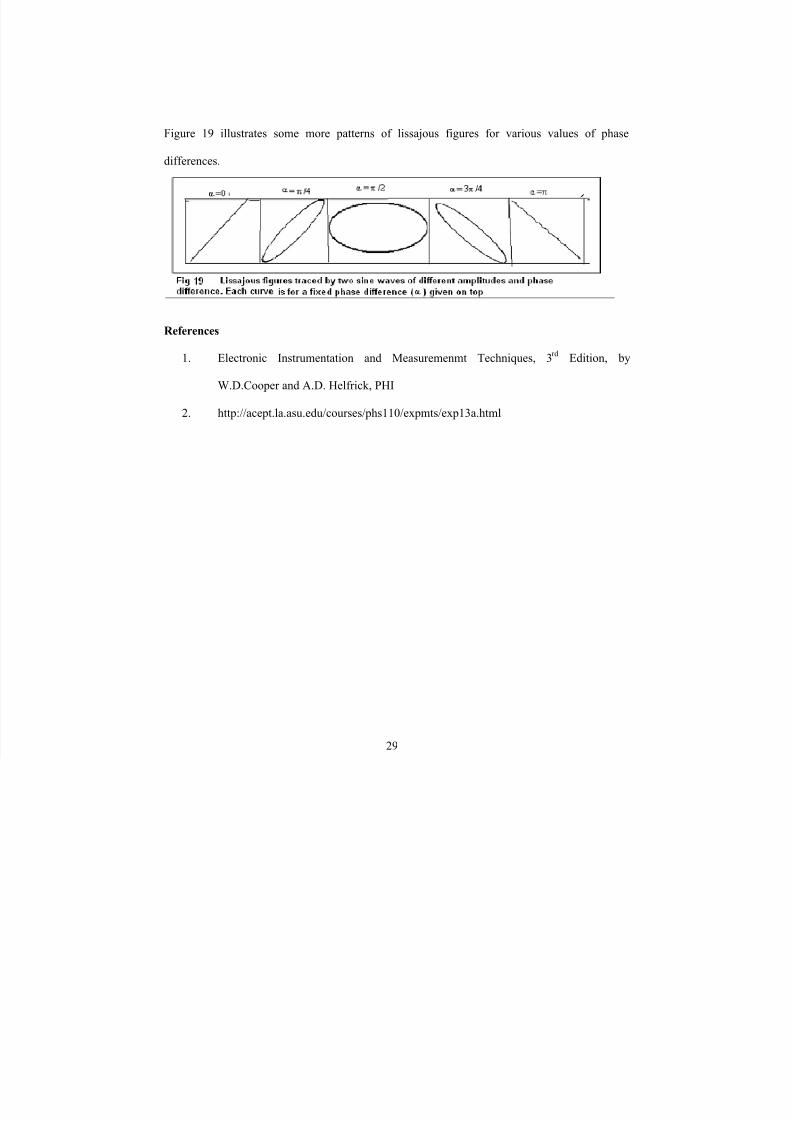
Figure 19 illustrates some more patterns of lissajous figures for various values of phase
differences.
References
1. Electronic Instrumentation and Measuremenmt Techniques, 3rd
Edition, by
W.D.Cooper and A.D. Helfrick, PHI
2. http://acept.la.asu.edu/courses/phs110/expmts/exp13a.html
Related Documents