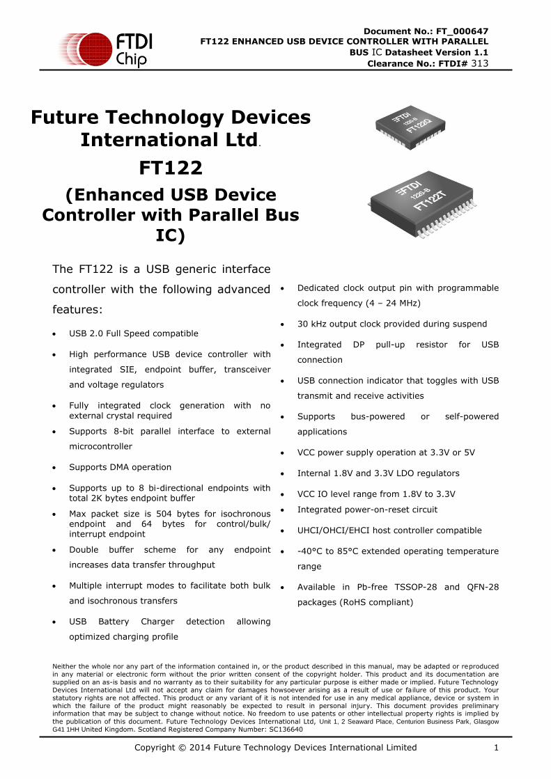
Copyright © 2014 Future Technology Devices International Limited 1 Document No.: FT_000647 FT122 ENHANCED USB DEVICE CONTROLLER WITH PARALLEL BUS IC Datasheet Version 1.1 Clearance No.: FTDI# 313 Future Technology Devices International Ltd. FT122 (Enhanced USB Device Controller with Parallel Bus IC) The FT122 is a USB generic interface controller with the following advanced features: USB 2.0 Full Speed compatible High performance USB device controller with integrated SIE, endpoint buffer, transceiver and voltage regulators Fully integrated clock generation with no external crystal required Supports 8-bit parallel interface to external microcontroller Supports DMA operation Supports up to 8 bi-directional endpoints with total 2K bytes endpoint buffer Max packet size is 504 bytes for isochronous endpoint and 64 bytes for control/bulk/ interrupt endpoint Double buffer scheme for any endpoint increases data transfer throughput Multiple interrupt modes to facilitate both bulk and isochronous transfers USB Battery Charger detection allowing optimized charging profile Dedicated clock output pin with programmable clock frequency (4 – 24 MHz) 30 kHz output clock provided during suspend Integrated DP pull-up resistor for USB connection USB connection indicator that toggles with USB transmit and receive activities Supports bus-powered or self-powered applications VCC power supply operation at 3.3V or 5V Internal 1.8V and 3.3V LDO regulators VCC IO level range from 1.8V to 3.3V Integrated power-on-reset circuit UHCI/OHCI/EHCI host controller compatible -40°C to 85°C extended operating temperature range Available in Pb-free TSSOP-28 and QFN-28 packages (RoHS compliant) Neither the whole nor any part of the information contained in, or the product described in this manual, may be adapted or reproduced in any material or electronic form without the prior written consent of the copyright holder. This product and its documentation are supplied on an as-is basis and no warranty as to their suitability for any particular purpose is either made or implied. Future Technology Devices International Ltd will not accept any claim for damages howsoever arising as a result of use or failure of this product. Your statutory rights are not affected. This product or any variant of it is not intended for use in any medical appliance, device or system in which the failure of the product might reasonably be expected to result in personal injury. This document provides preliminary information that may be subject to change without notice. No freedom to use patents or other intellectual property rights is implied by the publication of this document. Future Technology Devices International Ltd, Unit 1, 2 Seaward Place, Centurion Business Park, Glasgow G41 1HH United Kingdom. Scotland Registered Company Number: SC136640

Welcome message from author
This document is posted to help you gain knowledge. Please leave a comment to let me know what you think about it! Share it to your friends and learn new things together.
Transcript
Copyright © 2014 Future Technology Devices International Limited 1
Document No.: FT_000647 FT122 ENHANCED USB DEVICE CONTROLLER WITH PARALLEL
BUS IC Datasheet Version 1.1
Clearance No.: FTDI# 313
Future Technology Devices
International Ltd.
FT122
(Enhanced USB Device Controller with Parallel Bus
IC)
The FT122 is a USB generic interface
controller with the following advanced
features:
USB 2.0 Full Speed compatible
High performance USB device controller with
integrated SIE, endpoint buffer, transceiver
and voltage regulators
Fully integrated clock generation with no
external crystal required
Supports 8-bit parallel interface to external
microcontroller
Supports DMA operation
Supports up to 8 bi-directional endpoints with total 2K bytes endpoint buffer
Max packet size is 504 bytes for isochronous endpoint and 64 bytes for control/bulk/ interrupt endpoint
Double buffer scheme for any endpoint
increases data transfer throughput
Multiple interrupt modes to facilitate both bulk
and isochronous transfers
USB Battery Charger detection allowing
optimized charging profile
Dedicated clock output pin with programmable
clock frequency (4 – 24 MHz)
30 kHz output clock provided during suspend
Integrated DP pull-up resistor for USB
connection
USB connection indicator that toggles with USB
transmit and receive activities
Supports bus-powered or self-powered
applications
VCC power supply operation at 3.3V or 5V
Internal 1.8V and 3.3V LDO regulators
VCC IO level range from 1.8V to 3.3V
Integrated power-on-reset circuit
UHCI/OHCI/EHCI host controller compatible
-40°C to 85°C extended operating temperature
range
Available in Pb-free TSSOP-28 and QFN-28
packages (RoHS compliant)
Neither the whole nor any part of the information contained in, or the product described in this manual, may be adapted or reproduced
in any material or electronic form without the prior written consent of the copyright holder. This product and its documentation are
supplied on an as-is basis and no warranty as to their suitability for any particular purpose is either made or implied. Future Technology
Devices International Ltd will not accept any claim for damages howsoever arising as a result of use or failure of this product. Your
statutory rights are not affected. This product or any variant of it is not intended for use in any medical appliance, device or system in
which the failure of the product might reasonably be expected to result in personal injury. This document provides preliminary information that may be subject to change without notice. No freedom to use patents or other intellectual property rights is implied by
the publication of this document. Future Technology Devices International Ltd, Unit 1, 2 Seaward Place, Centurion Business Park, Glasgow
G41 1HH United Kingdom. Scotland Registered Company Number: SC136640
Copyright © 2014 Future Technology Devices International Limited 2
Document No.: FT_000647 FT122 ENHANCED USB DEVICE CONTROLLER WITH PARALLEL
BUS IC Datasheet Version 1.1
Clearance No.: FTDI# 313
1 Typical Applications
Provide USB port to Microcontrollers Provide USB port to FPGA’s
USB Industrial Control
Mass storage data transfers for multitude of
embedded systems applications, including
medical, industrial data-logger, power-
metering, and test instrumentation
Utilising USB to add system modularity
Isochronous support for video applications in
security, industrial control, and quality
inspections
1.1 Part Numbers
Part Number Package
FT122T-x TSSOP-28
FT122Q-x QFN-28
Note: Packaging codes for x is:
- R: Taped and Reel, (TSSOP is 2,500pcs per reel, QFN is 6,000pcs per reel).
- U: Tube packing, 50pcs per tube (TSSOP only)
- T: Tray packing, 490pcs per tray (QFN only)
For example: FT122T-R is 2,500pcs taped and reel packing
1.2 USB Compliant
At the time of writing this datasheet, the FT122 was in the process of completing USB compliance testing.
Copyright © 2014 Future Technology Devices International Limited 3
Document No.: FT_000647 FT122 ENHANCED USB DEVICE CONTROLLER WITH PARALLEL
BUS IC Datasheet Version 1.1
Clearance No.: FTDI# 313
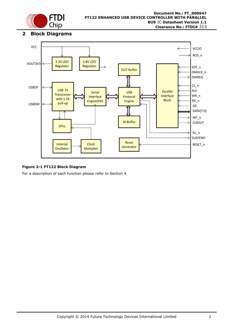
2 Block Diagrams
Figure 2-1 FT122 Block Diagram
For a description of each function please refer to Section 4.
Copyright © 2014 Future Technology Devices International Limited 4
Document No.: FT_000647 FT122 ENHANCED USB DEVICE CONTROLLER WITH PARALLEL
BUS IC Datasheet Version 1.1
Clearance No.: FTDI# 313
Table of Contents
1 Typical Applications ...................................................................... 2
1.1 Part Numbers...................................................................................... 2
1.2 USB Compliant .................................................................................... 2
2 Block Diagrams ............................................................................ 3
3 Device Pin Out and Signal Description .......................................... 6
3.1 TSSOP-28 Package Pin Out ................................................................. 6
3.2 QFN-28 Package Pin Out ..................................................................... 6
3.3 Pin Description ................................................................................... 7
4 Function Description..................................................................... 9
4.1 Functional Block Descriptions ............................................................. 9
4.2 Interrupt Modes ................................................................................ 10
5 Endpoint Buffer Management ..................................................... 11
5.1 Endpoint Buffer Management in Default Mode .................................. 11
5.2 Endpoint Buffer Management in Enhanced Mode .............................. 12
6 Commands and Registers ........................................................... 14
6.1 Command Summary .......................................................................... 14
6.2 Initialization Commands ................................................................... 19
6.2.1 Set Address Enable .................................................................................................... 19
6.2.2 Set Endpoint Enable ................................................................................................... 19
6.2.3 Set Mode .................................................................................................................. 19
6.2.4 Set DMA ................................................................................................................... 21
6.2.5 Set Endpoint Configuration (for Enhanced Mode) ........................................................... 22
6.3 Data Flow Commands ....................................................................... 23
6.3.1 Read Interrupt Register .............................................................................................. 23
6.3.2 Select Endpoint ......................................................................................................... 25
6.3.3 Read Last Transaction Status ...................................................................................... 25
6.3.4 Read Endpoint Status ................................................................................................. 26
6.3.5 Read Buffer ............................................................................................................... 27
6.3.6 Write Buffer .............................................................................................................. 27
6.3.7 Clear Buffer .............................................................................................................. 27
6.3.8 Validate Buffer .......................................................................................................... 28
6.3.9 Set Endpoint Status ................................................................................................... 28
6.3.10 Acknowledge Setup ................................................................................................ 28
6.4 General Commands ........................................................................... 28
6.4.1 Read Current Frame Number ....................................................................................... 29
6.4.2 Send Resume ............................................................................................................ 29
6.4.3 Set Buffer Interrupt Mode ........................................................................................... 29
6.4.4 Read Vendor ID ......................................................................................................... 30
Copyright © 2014 Future Technology Devices International Limited 5
Document No.: FT_000647 FT122 ENHANCED USB DEVICE CONTROLLER WITH PARALLEL
BUS IC Datasheet Version 1.1
Clearance No.: FTDI# 313
6.4.5 Read Product ID ........................................................................................................ 30
6.4.6 Read FTDI ID ............................................................................................................ 30
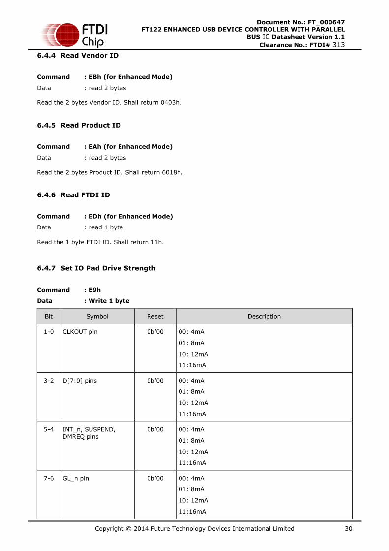
6.4.7 Set IO Pad Drive Strength........................................................................................... 30
7 Application Information ............................................................. 32
8 Devices Characteristics and Ratings ........................................... 33
8.1 Absolute Maximum Ratings............................................................... 33
8.2 DC Characteristics............................................................................. 34
8.3 AC Characteristics ............................................................................. 35
9 Package Parameters ................................................................... 39
9.1 TSSOP-28 Package Dimensions ........................................................ 39
9.2 TSSOP-28 Package Markings ........................................................... 40
9.3 QFN-28 Package Dimensions ............................................................ 41
9.4 QFN-28 Package Markings ............................................................... 42
9.5 Solder Reflow Profile ........................................................................ 42
10 Contact Information ................................................................... 44
Appendix A– References ............................................................................ 45
Appendix B - List of Figures and Tables ..................................................... 45
Appendix C - Revision History .................................................................... 47
Copyright © 2014 Future Technology Devices International Limited 6
Document No.: FT_000647 FT122 ENHANCED USB DEVICE CONTROLLER WITH PARALLEL
BUS IC Datasheet Version 1.1
Clearance No.: FTDI# 313
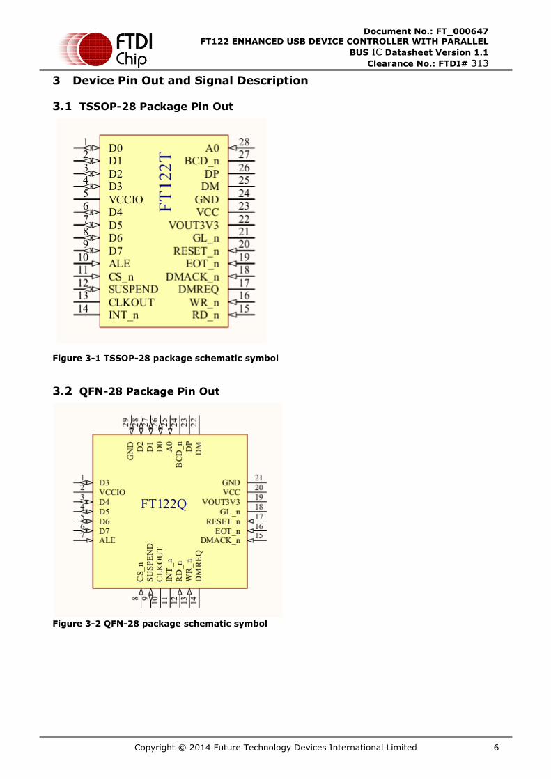
3 Device Pin Out and Signal Description
3.1 TSSOP-28 Package Pin Out
Figure 3-1 TSSOP-28 package schematic symbol
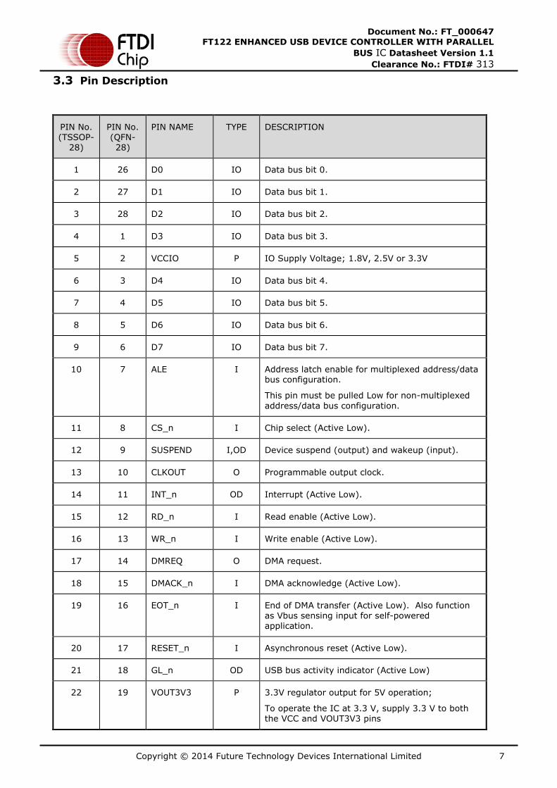
3.2 QFN-28 Package Pin Out
Figure 3-2 QFN-28 package schematic symbol
Copyright © 2014 Future Technology Devices International Limited 7
Document No.: FT_000647 FT122 ENHANCED USB DEVICE CONTROLLER WITH PARALLEL
BUS IC Datasheet Version 1.1
Clearance No.: FTDI# 313
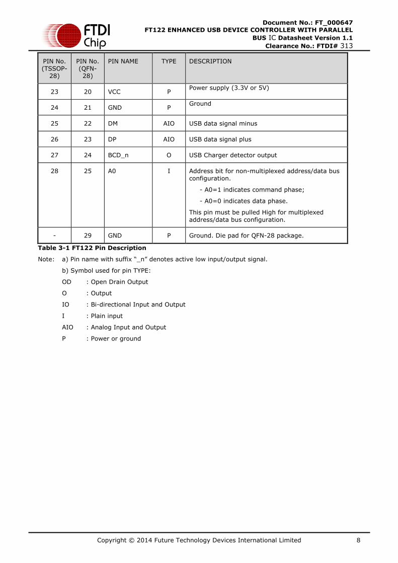
3.3 Pin Description
PIN No. (TSSOP-
28)
PIN No. (QFN-28)
PIN NAME TYPE DESCRIPTION
1 26 D0 IO Data bus bit 0.
2 27 D1 IO Data bus bit 1.
3 28 D2 IO Data bus bit 2.
4 1 D3 IO Data bus bit 3.
5 2 VCCIO P IO Supply Voltage; 1.8V, 2.5V or 3.3V
6 3 D4 IO Data bus bit 4.
7 4 D5 IO Data bus bit 5.
8 5 D6 IO Data bus bit 6.
9 6 D7 IO Data bus bit 7.
10 7 ALE I Address latch enable for multiplexed address/data bus configuration.
This pin must be pulled Low for non-multiplexed
address/data bus configuration.
11 8 CS_n I Chip select (Active Low).
12 9 SUSPEND I,OD Device suspend (output) and wakeup (input).
13 10 CLKOUT O Programmable output clock.
14 11 INT_n OD Interrupt (Active Low).
15 12 RD_n I Read enable (Active Low).
16 13 WR_n I Write enable (Active Low).
17 14 DMREQ O DMA request.
18 15 DMACK_n I DMA acknowledge (Active Low).
19 16 EOT_n I End of DMA transfer (Active Low). Also function
as Vbus sensing input for self-powered application.
20 17 RESET_n I Asynchronous reset (Active Low).
21 18 GL_n OD USB bus activity indicator (Active Low)
22 19 VOUT3V3 P 3.3V regulator output for 5V operation;
To operate the IC at 3.3 V, supply 3.3 V to both the VCC and VOUT3V3 pins
Copyright © 2014 Future Technology Devices International Limited 8
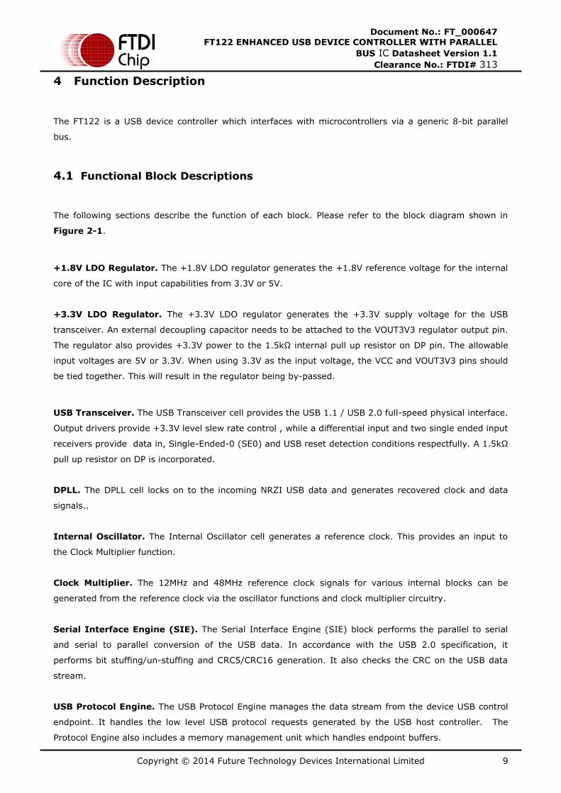
Document No.: FT_000647 FT122 ENHANCED USB DEVICE CONTROLLER WITH PARALLEL
BUS IC Datasheet Version 1.1
Clearance No.: FTDI# 313
PIN No. (TSSOP-
28)
PIN No. (QFN-28)
PIN NAME TYPE DESCRIPTION
23 20 VCC P Power supply (3.3V or 5V)
24 21 GND P Ground
25 22 DM AIO USB data signal minus
26 23 DP AIO USB data signal plus
27 24 BCD_n O USB Charger detector output
28 25 A0 I Address bit for non-multiplexed address/data bus configuration.
- A0=1 indicates command phase;
- A0=0 indicates data phase.
This pin must be pulled High for multiplexed
address/data bus configuration.
- 29 GND P Ground. Die pad for QFN-28 package.
Table 3-1 FT122 Pin Description
Note: a) Pin name with suffix “_n” denotes active low input/output signal.
b) Symbol used for pin TYPE:
OD : Open Drain Output
O : Output
IO : Bi-directional Input and Output
I : Plain input
AIO : Analog Input and Output
P : Power or ground
Copyright © 2014 Future Technology Devices International Limited 9
Document No.: FT_000647 FT122 ENHANCED USB DEVICE CONTROLLER WITH PARALLEL
BUS IC Datasheet Version 1.1
Clearance No.: FTDI# 313
4 Function Description
The FT122 is a USB device controller which interfaces with microcontrollers via a generic 8-bit parallel
bus.
4.1 Functional Block Descriptions
The following sections describe the function of each block. Please refer to the block diagram shown in
Figure 2-1.
+1.8V LDO Regulator. The +1.8V LDO regulator generates the +1.8V reference voltage for the internal
core of the IC with input capabilities from 3.3V or 5V.
+3.3V LDO Regulator. The +3.3V LDO regulator generates the +3.3V supply voltage for the USB
transceiver. An external decoupling capacitor needs to be attached to the VOUT3V3 regulator output pin.
The regulator also provides +3.3V power to the 1.5kΩ internal pull up resistor on DP pin. The allowable
input voltages are 5V or 3.3V. When using 3.3V as the input voltage, the VCC and VOUT3V3 pins should
be tied together. This will result in the regulator being by-passed.
USB Transceiver. The USB Transceiver cell provides the USB 1.1 / USB 2.0 full-speed physical interface.
Output drivers provide +3.3V level slew rate control , while a differential input and two single ended input
receivers provide data in, Single-Ended-0 (SE0) and USB reset detection conditions respectfully. A 1.5kΩ
pull up resistor on DP is incorporated.
DPLL. The DPLL cell locks on to the incoming NRZI USB data and generates recovered clock and data
signals..
Internal Oscillator. The Internal Oscillator cell generates a reference clock. This provides an input to
the Clock Multiplier function.
Clock Multiplier. The 12MHz and 48MHz reference clock signals for various internal blocks can be
generated from the reference clock via the oscillator functions and clock multiplier circuitry.
Serial Interface Engine (SIE). The Serial Interface Engine (SIE) block performs the parallel to serial
and serial to parallel conversion of the USB data. In accordance with the USB 2.0 specification, it
performs bit stuffing/un-stuffing and CRC5/CRC16 generation. It also checks the CRC on the USB data
stream.
USB Protocol Engine. The USB Protocol Engine manages the data stream from the device USB control
endpoint. It handles the low level USB protocol requests generated by the USB host controller. The
Protocol Engine also includes a memory management unit which handles endpoint buffers.
Copyright © 2014 Future Technology Devices International Limited 10
Document No.: FT_000647 FT122 ENHANCED USB DEVICE CONTROLLER WITH PARALLEL
BUS IC Datasheet Version 1.1
Clearance No.: FTDI# 313
OUT Buffer. Data sent from the USB host controller to FT122 via the USB data OUT endpoint is stored in
the OUT buffer. Data is removed from the OUT buffer to system memory under control of the parallel
interface block.
IN Buffer. Data from system memory is stored in the IN buffer. The USB host controller removes data
from the IN buffer by sending a USB request for data from the device data IN endpoint.
RESET Generator. The integrated Reset Generator cell provides a reliable power-on reset to the device
internal circuitry at power up. The RESET_n input pin allows an external device to reset the FT122.
Parallel Interface Block. The 8-bit parallel bus allows direct interface to a generic microcontroller
(MCU), supporting both multiplexed and non-multiplexed address/data bus configurations. The FT122
also supports Direct Memory Access (DMA) operation. With DMA access data can be written to the IN
buffer or read from the OUT buffer without MCU intervention. The DMA access can be done in single cycle
or burst mode.
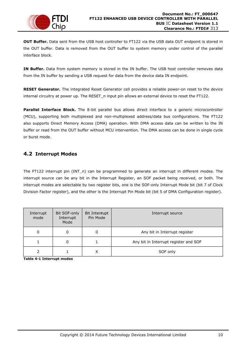
4.2 Interrupt Modes
The FT122 interrupt pin (INT_n) can be programmed to generate an interrupt in different modes. The
interrupt source can be any bit in the Interrupt Register, an SOF packet being received, or both. The
interrupt modes are selectable by two register bits, one is the SOF-only Interrupt Mode bit (bit 7 of Clock
Division Factor register), and the other is the Interrupt Pin Mode bit (bit 5 of DMA Configuration register).
Interrupt
mode
Bit SOF-only
Interrupt Mode
Bit Interrupt
Pin Mode
Interrupt source
0 0 0 Any bit in Interrupt register
1 0 1 Any bit in Interrupt register and SOF
2 1 X SOF only
Table 4-1 Interrupt modes
Copyright © 2014 Future Technology Devices International Limited 11
Document No.: FT_000647 FT122 ENHANCED USB DEVICE CONTROLLER WITH PARALLEL
BUS IC Datasheet Version 1.1
Clearance No.: FTDI# 313
5 Endpoint Buffer Management
The FT122 has 2 modes of operation for command and memory management: the default mode (FT120
compatible mode) and the enhanced mode. The buffer management schemes are different in these two
modes. Upon reset the default mode is functional. The enhanced mode is activated when any of the Set
Endpoint Configuration commands (B0h – BFh) are received.
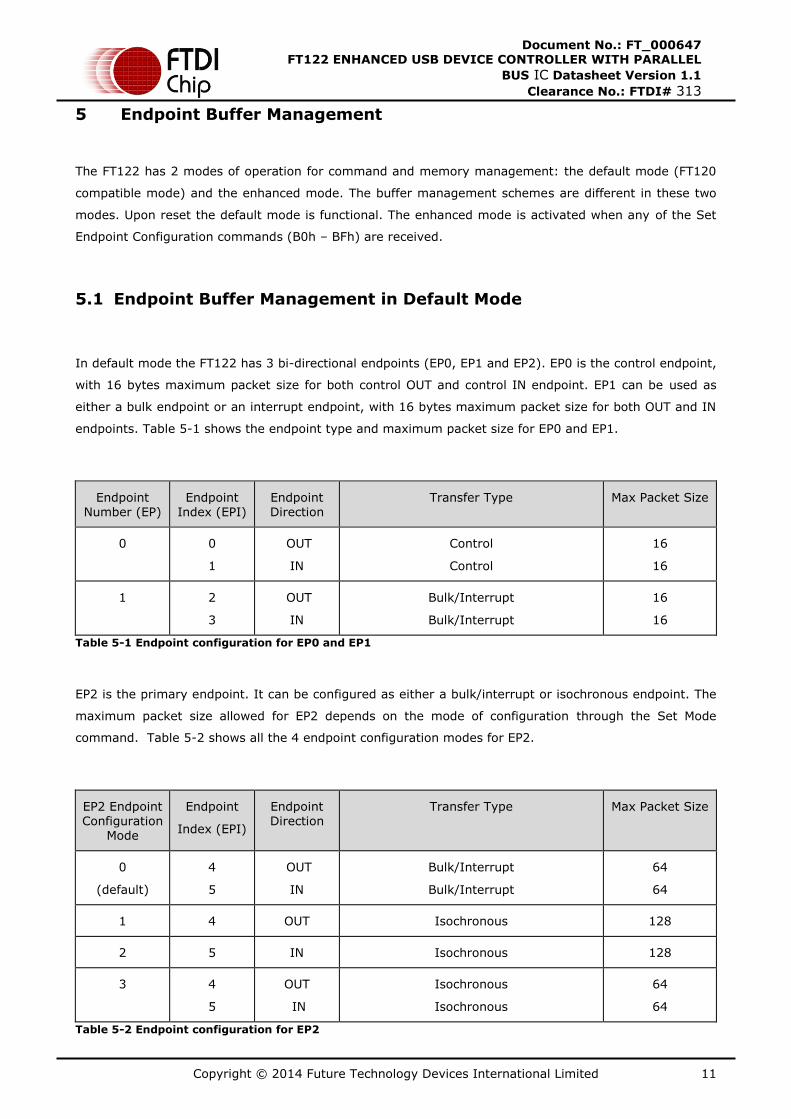
5.1 Endpoint Buffer Management in Default Mode
In default mode the FT122 has 3 bi-directional endpoints (EP0, EP1 and EP2). EP0 is the control endpoint,
with 16 bytes maximum packet size for both control OUT and control IN endpoint. EP1 can be used as
either a bulk endpoint or an interrupt endpoint, with 16 bytes maximum packet size for both OUT and IN
endpoints. Table 5-1 shows the endpoint type and maximum packet size for EP0 and EP1.
Endpoint Number (EP)
Endpoint Index (EPI)
Endpoint Direction
Transfer Type Max Packet Size
0
0
1
OUT
IN
Control
Control
16
16
1
2
3
OUT
IN
Bulk/Interrupt
Bulk/Interrupt
16
16
Table 5-1 Endpoint configuration for EP0 and EP1
EP2 is the primary endpoint. It can be configured as either a bulk/interrupt or isochronous endpoint. The
maximum packet size allowed for EP2 depends on the mode of configuration through the Set Mode
command. Table 5-2 shows all the 4 endpoint configuration modes for EP2.
EP2 Endpoint Configuration
Mode
Endpoint
Index (EPI)
Endpoint Direction
Transfer Type Max Packet Size
0
(default)
4
5
OUT
IN
Bulk/Interrupt
Bulk/Interrupt
64
64
1 4 OUT Isochronous 128
2 5 IN Isochronous 128
3 4
5
OUT
IN
Isochronous
Isochronous
64
64
Table 5-2 Endpoint configuration for EP2
Copyright © 2014 Future Technology Devices International Limited 12
Document No.: FT_000647 FT122 ENHANCED USB DEVICE CONTROLLER WITH PARALLEL
BUS IC Datasheet Version 1.1
Clearance No.: FTDI# 313
As the primary endpoint, EP2 is suitable for transmitting or receiving relatively large data. To improve the
data throughput, EP2 is implemented with double buffering. This allows the concurrent operation between
USB bus access and MCU or DMA local bus access. For example, for EP2 IN endpoint (EPI5), the USB host
can read data from FT122 Buffer 0 while the local MCU is writing to Buffer 1 at the same time. The USB
host can subsequently read from FT122 Buffer 1 without waiting for it to be filled. Buffer switching is
handled automatically by the FT122.
The EP2 buffer also supports DMA operation. The MCU needs to initialize the DMA operation through the
Set DMA command. Once DMA operation is enabled, data will be moving between the system memory
and FT122 endpoint buffer under the DMA controller. Buffer switching between Buffer 0 and Buffer 1 is
handled automatically.
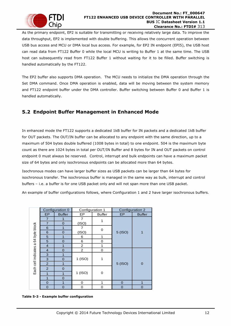
5.2 Endpoint Buffer Management in Enhanced Mode
In enhanced mode the FT122 supports a dedicated 1kB buffer for IN packets and a dedicated 1kB buffer
for OUT packets. The OUT/IN buffer can be allocated to any endpoint with the same direction, up to a
maximum of 504 bytes double buffered (1008 bytes in total) to one endpoint. 504 is the maximum byte
count as there are 1024 bytes in total per OUT/IN Buffer and 8 bytes for IN and OUT packets on control
endpoint 0 must always be reserved. Control, interrupt and bulk endpoints can have a maximum packet
size of 64 bytes and only isochronous endpoints can be allocated more than 64 bytes.
Isochronous modes can have larger buffer sizes as USB packets can be larger than 64 bytes for
isochronous transfer. The isochronous buffer is managed in the same way as bulk, interrupt and control
buffers – i.e. a buffer is for one USB packet only and will not span more than one USB packet.
An example of buffer configurations follows, where Configuration 1 and 2 have larger isochronous buffers.
Table 5-3 - Example buffer configuration
EP Buffer EP Buffer EP Buffer
7 1
7 0
6 1
6 0 5 (ISO) 1
5 1 6 1
5 0 6 0
4 1 2 1
4 0 2 0
3 1
3 0
2 1 5 (ISO) 0
2 0
1 1
1 0
0 1 0 1 0 1
0 0 0 0 0 0
0
1
1 (ISO) 0
11 (ISO)
Configuration 2
Ea
ch c
ell
ind
ica
tes
a 6
4 b
yte
blo
ck
Configuration 0 Configuration 1
7
(ISO)
7
(ISO)
Copyright © 2014 Future Technology Devices International Limited 13
Document No.: FT_000647 FT122 ENHANCED USB DEVICE CONTROLLER WITH PARALLEL
BUS IC Datasheet Version 1.1
Clearance No.: FTDI# 313
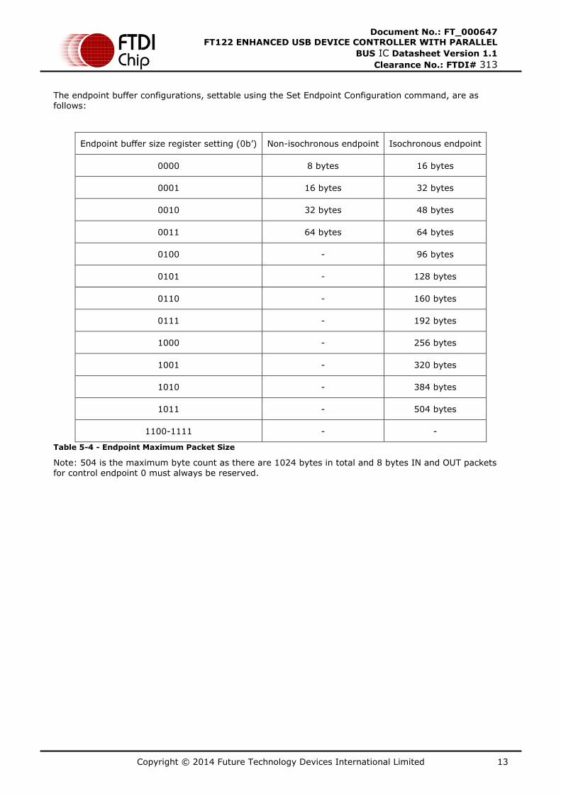
The endpoint buffer configurations, settable using the Set Endpoint Configuration command, are as follows:
Endpoint buffer size register setting (0b’) Non-isochronous endpoint Isochronous endpoint
0000 8 bytes 16 bytes
0001 16 bytes 32 bytes
0010 32 bytes 48 bytes
0011 64 bytes 64 bytes
0100 - 96 bytes
0101 - 128 bytes
0110 - 160 bytes
0111 - 192 bytes
1000 - 256 bytes
1001 - 320 bytes
1010 - 384 bytes
1011 - 504 bytes
1100-1111 - -
Table 5-4 - Endpoint Maximum Packet Size
Note: 504 is the maximum byte count as there are 1024 bytes in total and 8 bytes IN and OUT packets for control endpoint 0 must always be reserved.
Copyright © 2014 Future Technology Devices International Limited 14
Document No.: FT_000647 FT122 ENHANCED USB DEVICE CONTROLLER WITH PARALLEL
BUS IC Datasheet Version 1.1
Clearance No.: FTDI# 313
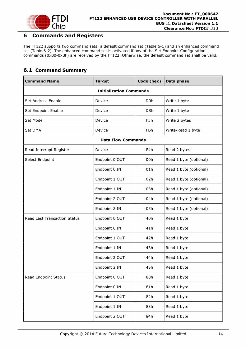
6 Commands and Registers
The FT122 supports two command sets: a default command set (Table 6-1) and an enhanced command set (Table 6-2). The enhanced command set is activated if any of the Set Endpoint Configuration commands (0xB0-0xBF) are received by the FT122. Otherwise, the default command set shall be valid.
6.1 Command Summary
Command Name Target Code (hex) Data phase
Initialization Commands
Set Address Enable Device D0h Write 1 byte
Set Endpoint Enable Device D8h Write 1 byte
Set Mode Device F3h Write 2 bytes
Set DMA Device FBh Write/Read 1 byte
Data Flow Commands
Read Interrupt Register Device F4h Read 2 bytes
Select Endpoint Endpoint 0 OUT 00h Read 1 byte (optional)
Endpoint 0 IN 01h Read 1 byte (optional)
Endpoint 1 OUT 02h Read 1 byte (optional)
Endpoint 1 IN 03h Read 1 byte (optional)
Endpoint 2 OUT 04h Read 1 byte (optional)
Endpoint 2 IN 05h Read 1 byte (optional)
Read Last Transaction Status Endpoint 0 OUT 40h Read 1 byte
Endpoint 0 IN 41h Read 1 byte
Endpoint 1 OUT 42h Read 1 byte
Endpoint 1 IN 43h Read 1 byte
Endpoint 2 OUT 44h Read 1 byte
Endpoint 2 IN 45h Read 1 byte
Read Endpoint Status Endpoint 0 OUT 80h Read 1 byte
Endpoint 0 IN 81h Read 1 byte
Endpoint 1 OUT 82h Read 1 byte
Endpoint 1 IN 83h Read 1 byte
Endpoint 2 OUT 84h Read 1 byte
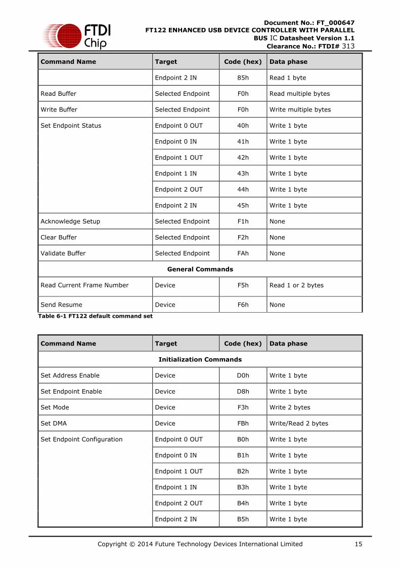
Copyright © 2014 Future Technology Devices International Limited 15
Document No.: FT_000647 FT122 ENHANCED USB DEVICE CONTROLLER WITH PARALLEL
BUS IC Datasheet Version 1.1
Clearance No.: FTDI# 313
Command Name Target Code (hex) Data phase
Endpoint 2 IN 85h Read 1 byte
Read Buffer Selected Endpoint F0h Read multiple bytes
Write Buffer Selected Endpoint F0h Write multiple bytes
Set Endpoint Status Endpoint 0 OUT 40h Write 1 byte
Endpoint 0 IN 41h Write 1 byte
Endpoint 1 OUT 42h Write 1 byte
Endpoint 1 IN 43h Write 1 byte
Endpoint 2 OUT 44h Write 1 byte
Endpoint 2 IN 45h Write 1 byte
Acknowledge Setup Selected Endpoint F1h None
Clear Buffer Selected Endpoint F2h None
Validate Buffer Selected Endpoint FAh None
General Commands
Read Current Frame Number Device F5h Read 1 or 2 bytes
Send Resume Device F6h None
Table 6-1 FT122 default command set
Command Name Target Code (hex) Data phase
Initialization Commands
Set Address Enable Device D0h Write 1 byte
Set Endpoint Enable Device D8h Write 1 byte
Set Mode Device F3h Write 2 bytes
Set DMA Device FBh Write/Read 2 bytes
Set Endpoint Configuration Endpoint 0 OUT B0h Write 1 byte
Endpoint 0 IN B1h Write 1 byte
Endpoint 1 OUT B2h Write 1 byte
Endpoint 1 IN B3h Write 1 byte
Endpoint 2 OUT B4h Write 1 byte
Endpoint 2 IN B5h Write 1 byte
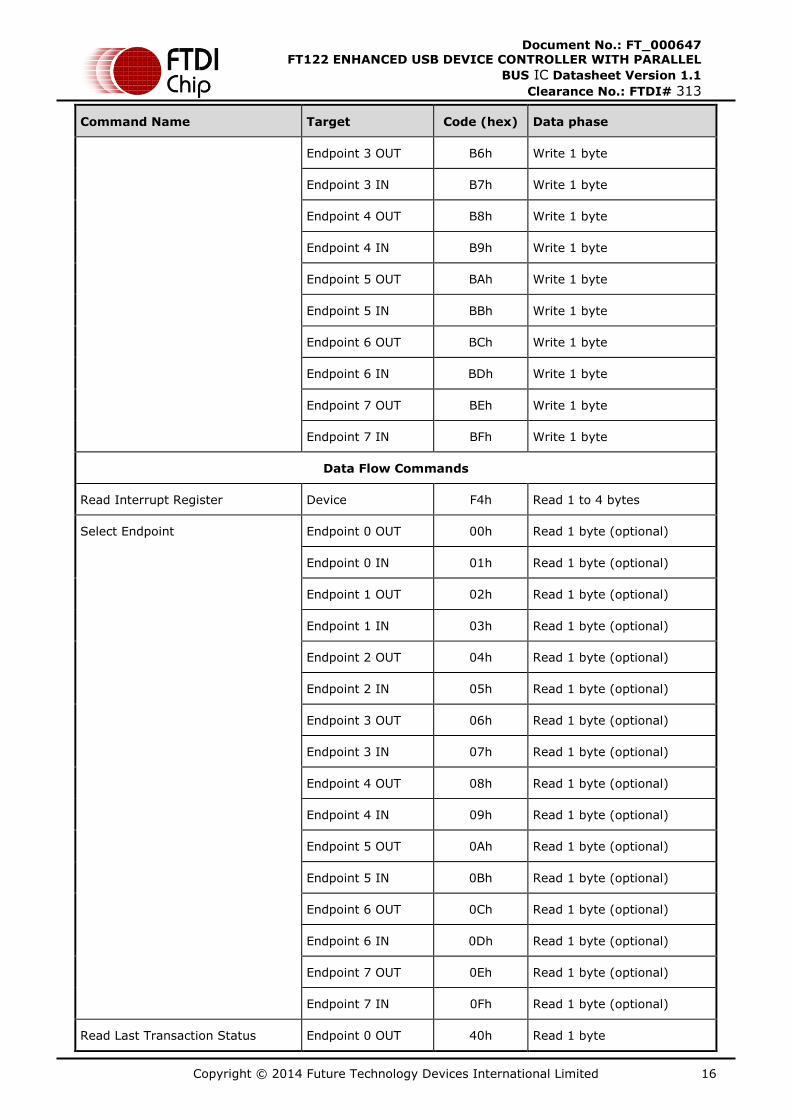
Copyright © 2014 Future Technology Devices International Limited 16
Document No.: FT_000647 FT122 ENHANCED USB DEVICE CONTROLLER WITH PARALLEL
BUS IC Datasheet Version 1.1
Clearance No.: FTDI# 313
Command Name Target Code (hex) Data phase
Endpoint 3 OUT B6h Write 1 byte
Endpoint 3 IN B7h Write 1 byte
Endpoint 4 OUT B8h Write 1 byte
Endpoint 4 IN B9h Write 1 byte
Endpoint 5 OUT BAh Write 1 byte
Endpoint 5 IN BBh Write 1 byte
Endpoint 6 OUT BCh Write 1 byte
Endpoint 6 IN BDh Write 1 byte
Endpoint 7 OUT BEh Write 1 byte
Endpoint 7 IN BFh Write 1 byte
Data Flow Commands
Read Interrupt Register Device F4h Read 1 to 4 bytes
Select Endpoint Endpoint 0 OUT 00h Read 1 byte (optional)
Endpoint 0 IN 01h Read 1 byte (optional)
Endpoint 1 OUT 02h Read 1 byte (optional)
Endpoint 1 IN 03h Read 1 byte (optional)
Endpoint 2 OUT 04h Read 1 byte (optional)
Endpoint 2 IN 05h Read 1 byte (optional)
Endpoint 3 OUT 06h Read 1 byte (optional)
Endpoint 3 IN 07h Read 1 byte (optional)
Endpoint 4 OUT 08h Read 1 byte (optional)
Endpoint 4 IN 09h Read 1 byte (optional)
Endpoint 5 OUT 0Ah Read 1 byte (optional)
Endpoint 5 IN 0Bh Read 1 byte (optional)
Endpoint 6 OUT 0Ch Read 1 byte (optional)
Endpoint 6 IN 0Dh Read 1 byte (optional)
Endpoint 7 OUT 0Eh Read 1 byte (optional)
Endpoint 7 IN 0Fh Read 1 byte (optional)
Read Last Transaction Status Endpoint 0 OUT 40h Read 1 byte
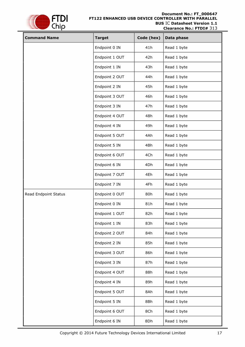
Copyright © 2014 Future Technology Devices International Limited 17
Document No.: FT_000647 FT122 ENHANCED USB DEVICE CONTROLLER WITH PARALLEL
BUS IC Datasheet Version 1.1
Clearance No.: FTDI# 313
Command Name Target Code (hex) Data phase
Endpoint 0 IN 41h Read 1 byte
Endpoint 1 OUT 42h Read 1 byte
Endpoint 1 IN 43h Read 1 byte
Endpoint 2 OUT 44h Read 1 byte
Endpoint 2 IN 45h Read 1 byte
Endpoint 3 OUT 46h Read 1 byte
Endpoint 3 IN 47h Read 1 byte
Endpoint 4 OUT 48h Read 1 byte
Endpoint 4 IN 49h Read 1 byte
Endpoint 5 OUT 4Ah Read 1 byte
Endpoint 5 IN 4Bh Read 1 byte
Endpoint 6 OUT 4Ch Read 1 byte
Endpoint 6 IN 4Dh Read 1 byte
Endpoint 7 OUT 4Eh Read 1 byte
Endpoint 7 IN 4Fh Read 1 byte
Read Endpoint Status Endpoint 0 OUT 80h Read 1 byte
Endpoint 0 IN 81h Read 1 byte
Endpoint 1 OUT 82h Read 1 byte
Endpoint 1 IN 83h Read 1 byte
Endpoint 2 OUT 84h Read 1 byte
Endpoint 2 IN 85h Read 1 byte
Endpoint 3 OUT 86h Read 1 byte
Endpoint 3 IN 87h Read 1 byte
Endpoint 4 OUT 88h Read 1 byte
Endpoint 4 IN 89h Read 1 byte
Endpoint 5 OUT 8Ah Read 1 byte
Endpoint 5 IN 8Bh Read 1 byte
Endpoint 6 OUT 8Ch Read 1 byte
Endpoint 6 IN 8Dh Read 1 byte
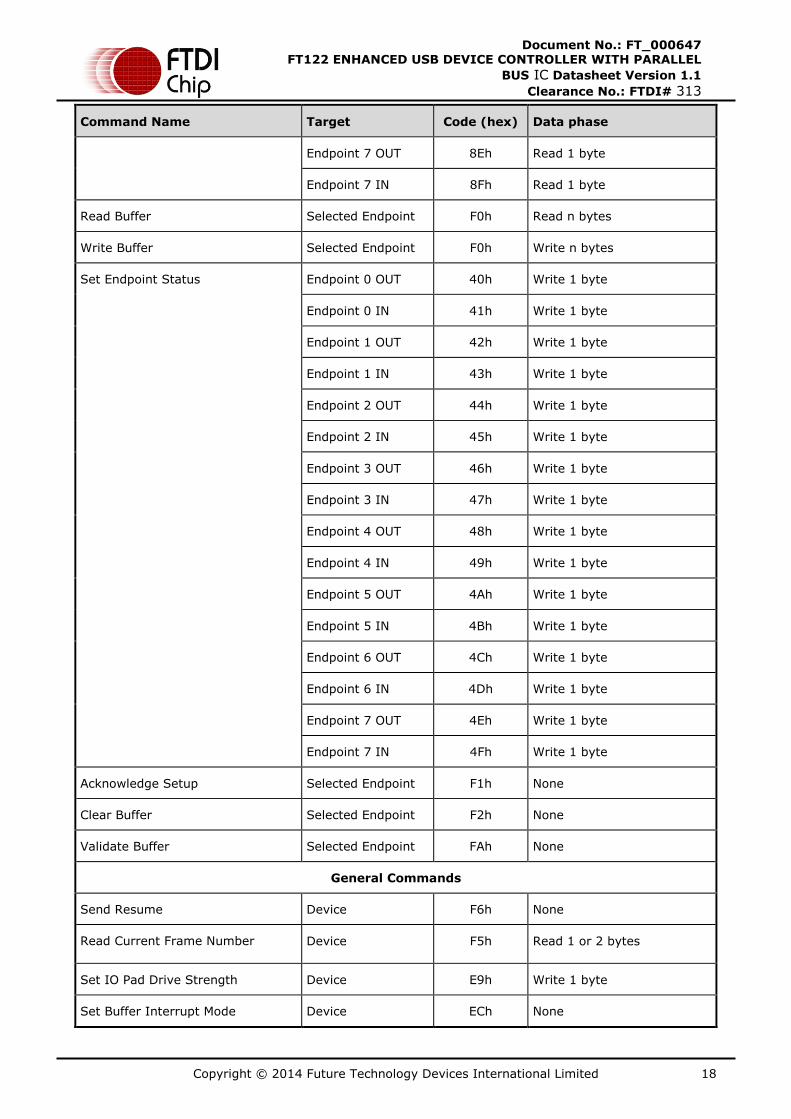
Copyright © 2014 Future Technology Devices International Limited 18
Document No.: FT_000647 FT122 ENHANCED USB DEVICE CONTROLLER WITH PARALLEL
BUS IC Datasheet Version 1.1
Clearance No.: FTDI# 313
Command Name Target Code (hex) Data phase
Endpoint 7 OUT 8Eh Read 1 byte
Endpoint 7 IN 8Fh Read 1 byte
Read Buffer Selected Endpoint F0h Read n bytes
Write Buffer Selected Endpoint F0h Write n bytes
Set Endpoint Status Endpoint 0 OUT 40h Write 1 byte
Endpoint 0 IN 41h Write 1 byte
Endpoint 1 OUT 42h Write 1 byte
Endpoint 1 IN 43h Write 1 byte
Endpoint 2 OUT 44h Write 1 byte
Endpoint 2 IN 45h Write 1 byte
Endpoint 3 OUT 46h Write 1 byte
Endpoint 3 IN 47h Write 1 byte
Endpoint 4 OUT 48h Write 1 byte
Endpoint 4 IN 49h Write 1 byte
Endpoint 5 OUT 4Ah Write 1 byte
Endpoint 5 IN 4Bh Write 1 byte
Endpoint 6 OUT 4Ch Write 1 byte
Endpoint 6 IN 4Dh Write 1 byte
Endpoint 7 OUT 4Eh Write 1 byte
Endpoint 7 IN 4Fh Write 1 byte
Acknowledge Setup Selected Endpoint F1h None
Clear Buffer Selected Endpoint F2h None
Validate Buffer Selected Endpoint FAh None
General Commands
Send Resume Device F6h None
Read Current Frame Number Device F5h Read 1 or 2 bytes
Set IO Pad Drive Strength Device E9h Write 1 byte
Set Buffer Interrupt Mode Device ECh None
Copyright © 2014 Future Technology Devices International Limited 19
Document No.: FT_000647 FT122 ENHANCED USB DEVICE CONTROLLER WITH PARALLEL
BUS IC Datasheet Version 1.1
Clearance No.: FTDI# 313
Command Name Target Code (hex) Data phase
Read Vendor ID Device EBh Read 2 bytes
Read Product ID Device EAh Read 2 bytes
Read FTDI ID Device EDh Read 1 byte
Table 6-2 enhanced command set
6.2 Initialization Commands
6.2.1 Set Address Enable
Command : D0h
Data : Write 1 byte
Bit Symbol Reset Description
6-0 Address 0b’0000000 USB assigned device address. A bus reset will reset all address bits to 0.
7 Enable 0 Function enable. A bus reset will automatically enable the function at default address 0.
Table 6-3 Address Enable Register
6.2.2 Set Endpoint Enable
Command : D8h
Data : Write 1 byte
Bit Symbol Reset Description
0 EP_Enable 0 Enable all endpoints (Note EP0 is always enabled regardless the setting of EP_Enable bit). Endpoints can only be enabled when the function is enabled.
7-1 Reserved 0b’0000000 Reserved, write to 0
Table 6-4 Endpoint Enable Register
6.2.3 Set Mode
Command : F3h
Data : Write 2 bytes
Bit Symbol Reset Description
0 Reserved 0 Reserved, write to 0
1 No Suspend Clock 1 0: CLKOUT switches to 30 KHz during USB suspend
Copyright © 2014 Future Technology Devices International Limited 20
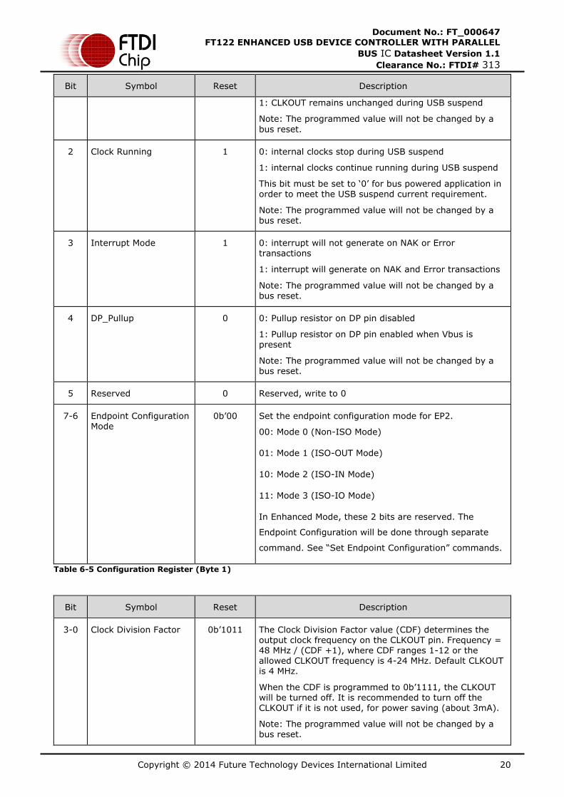
Document No.: FT_000647 FT122 ENHANCED USB DEVICE CONTROLLER WITH PARALLEL
BUS IC Datasheet Version 1.1
Clearance No.: FTDI# 313
Bit Symbol Reset Description
1: CLKOUT remains unchanged during USB suspend
Note: The programmed value will not be changed by a
bus reset.
2 Clock Running 1 0: internal clocks stop during USB suspend
1: internal clocks continue running during USB suspend
This bit must be set to ‘0’ for bus powered application in order to meet the USB suspend current requirement.
Note: The programmed value will not be changed by a bus reset.
3 Interrupt Mode 1 0: interrupt will not generate on NAK or Error transactions
1: interrupt will generate on NAK and Error transactions
Note: The programmed value will not be changed by a bus reset.
4 DP_Pullup 0 0: Pullup resistor on DP pin disabled
1: Pullup resistor on DP pin enabled when Vbus is present
Note: The programmed value will not be changed by a bus reset.
5 Reserved 0 Reserved, write to 0
7-6 Endpoint Configuration Mode
0b’00 Set the endpoint configuration mode for EP2.
00: Mode 0 (Non-ISO Mode)
01: Mode 1 (ISO-OUT Mode)
10: Mode 2 (ISO-IN Mode)
11: Mode 3 (ISO-IO Mode)
In Enhanced Mode, these 2 bits are reserved. The
Endpoint Configuration will be done through separate
command. See “Set Endpoint Configuration” commands.
Table 6-5 Configuration Register (Byte 1)
Bit Symbol Reset Description
3-0 Clock Division Factor 0b’1011 The Clock Division Factor value (CDF) determines the output clock frequency on the CLKOUT pin. Frequency = 48 MHz / (CDF +1), where CDF ranges 1-12 or the allowed CLKOUT frequency is 4-24 MHz. Default CLKOUT is 4 MHz.
When the CDF is programmed to 0b’1111, the CLKOUT will be turned off. It is recommended to turn off the CLKOUT if it is not used, for power saving (about 3mA).
Note: The programmed value will not be changed by a bus reset.
Copyright © 2014 Future Technology Devices International Limited 21
Document No.: FT_000647 FT122 ENHANCED USB DEVICE CONTROLLER WITH PARALLEL
BUS IC Datasheet Version 1.1
Clearance No.: FTDI# 313
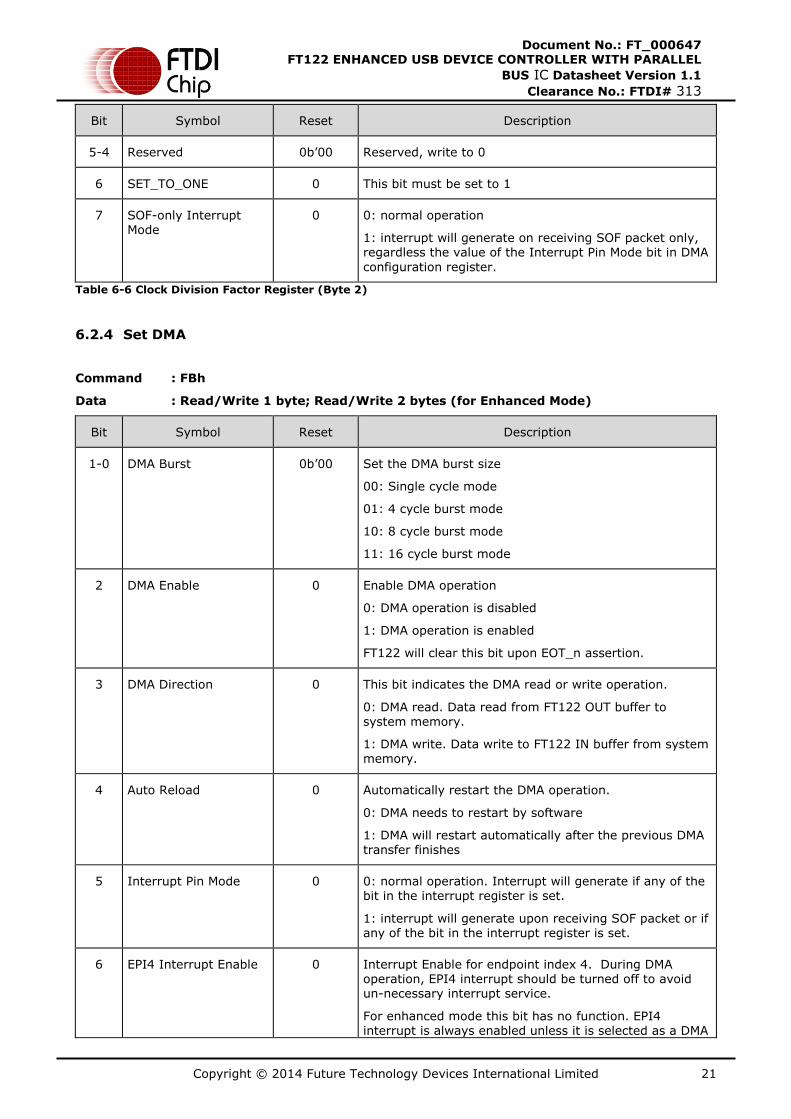
Bit Symbol Reset Description
5-4 Reserved 0b’00 Reserved, write to 0
6 SET_TO_ONE 0 This bit must be set to 1
7 SOF-only Interrupt Mode
0 0: normal operation
1: interrupt will generate on receiving SOF packet only, regardless the value of the Interrupt Pin Mode bit in DMA
configuration register.
Table 6-6 Clock Division Factor Register (Byte 2)
6.2.4 Set DMA
Command : FBh
Data : Read/Write 1 byte; Read/Write 2 bytes (for Enhanced Mode)
Bit Symbol Reset Description
1-0 DMA Burst 0b’00 Set the DMA burst size
00: Single cycle mode
01: 4 cycle burst mode
10: 8 cycle burst mode
11: 16 cycle burst mode
2 DMA Enable 0 Enable DMA operation
0: DMA operation is disabled
1: DMA operation is enabled
FT122 will clear this bit upon EOT_n assertion.
3 DMA Direction 0 This bit indicates the DMA read or write operation.
0: DMA read. Data read from FT122 OUT buffer to system memory.
1: DMA write. Data write to FT122 IN buffer from system memory.
4 Auto Reload 0 Automatically restart the DMA operation.
0: DMA needs to restart by software
1: DMA will restart automatically after the previous DMA transfer finishes
5 Interrupt Pin Mode 0 0: normal operation. Interrupt will generate if any of the bit in the interrupt register is set.
1: interrupt will generate upon receiving SOF packet or if any of the bit in the interrupt register is set.
6 EPI4 Interrupt Enable 0 Interrupt Enable for endpoint index 4. During DMA operation, EPI4 interrupt should be turned off to avoid un-necessary interrupt service.
For enhanced mode this bit has no function. EPI4 interrupt is always enabled unless it is selected as a DMA
Copyright © 2014 Future Technology Devices International Limited 22
Document No.: FT_000647 FT122 ENHANCED USB DEVICE CONTROLLER WITH PARALLEL
BUS IC Datasheet Version 1.1
Clearance No.: FTDI# 313
Bit Symbol Reset Description
endpoint.
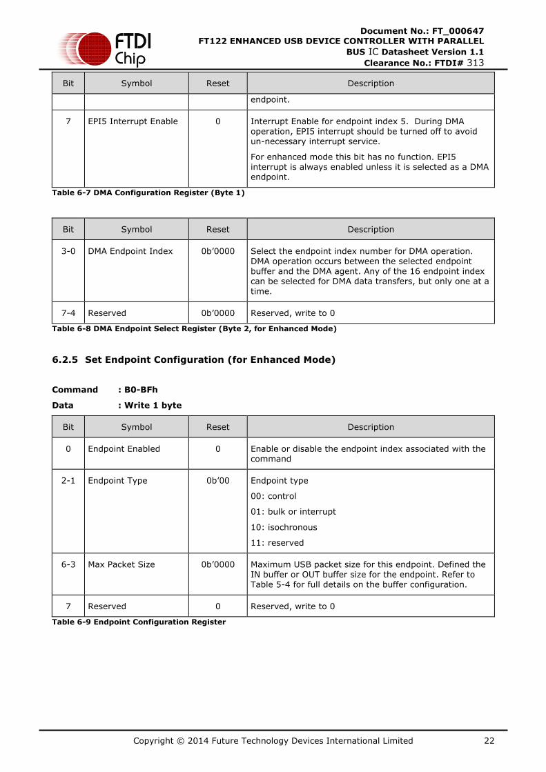
7 EPI5 Interrupt Enable 0 Interrupt Enable for endpoint index 5. During DMA operation, EPI5 interrupt should be turned off to avoid un-necessary interrupt service.
For enhanced mode this bit has no function. EPI5 interrupt is always enabled unless it is selected as a DMA endpoint.
Table 6-7 DMA Configuration Register (Byte 1)
Bit Symbol Reset Description
3-0 DMA Endpoint Index 0b’0000 Select the endpoint index number for DMA operation.
DMA operation occurs between the selected endpoint buffer and the DMA agent. Any of the 16 endpoint index can be selected for DMA data transfers, but only one at a time.
7-4 Reserved 0b’0000 Reserved, write to 0
Table 6-8 DMA Endpoint Select Register (Byte 2, for Enhanced Mode)
6.2.5 Set Endpoint Configuration (for Enhanced Mode)
Command : B0-BFh
Data : Write 1 byte
Bit Symbol Reset Description
0 Endpoint Enabled 0 Enable or disable the endpoint index associated with the command
2-1 Endpoint Type 0b’00 Endpoint type
00: control
01: bulk or interrupt
10: isochronous
11: reserved
6-3 Max Packet Size 0b’0000 Maximum USB packet size for this endpoint. Defined the IN buffer or OUT buffer size for the endpoint. Refer to Table 5-4 for full details on the buffer configuration.
7 Reserved 0 Reserved, write to 0
Table 6-9 Endpoint Configuration Register
Copyright © 2014 Future Technology Devices International Limited 23
Document No.: FT_000647 FT122 ENHANCED USB DEVICE CONTROLLER WITH PARALLEL
BUS IC Datasheet Version 1.1
Clearance No.: FTDI# 313
6.3 Data Flow Commands
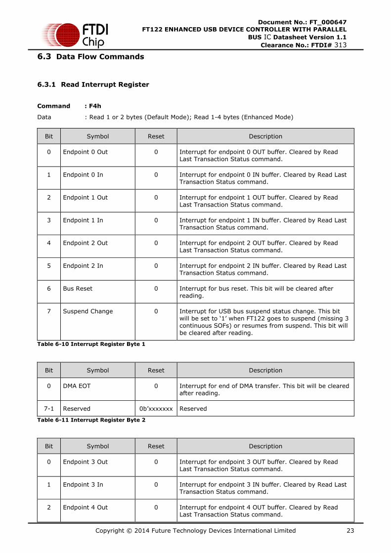
6.3.1 Read Interrupt Register
Command : F4h
Data : Read 1 or 2 bytes (Default Mode); Read 1-4 bytes (Enhanced Mode)
Bit Symbol Reset Description
0 Endpoint 0 Out 0 Interrupt for endpoint 0 OUT buffer. Cleared by Read Last Transaction Status command.
1 Endpoint 0 In 0 Interrupt for endpoint 0 IN buffer. Cleared by Read Last Transaction Status command.
2 Endpoint 1 Out 0 Interrupt for endpoint 1 OUT buffer. Cleared by Read
Last Transaction Status command.
3 Endpoint 1 In 0 Interrupt for endpoint 1 IN buffer. Cleared by Read Last Transaction Status command.
4 Endpoint 2 Out 0 Interrupt for endpoint 2 OUT buffer. Cleared by Read
Last Transaction Status command.
5 Endpoint 2 In 0 Interrupt for endpoint 2 IN buffer. Cleared by Read Last Transaction Status command.
6 Bus Reset 0 Interrupt for bus reset. This bit will be cleared after reading.
7 Suspend Change 0 Interrupt for USB bus suspend status change. This bit will be set to ‘1’ when FT122 goes to suspend (missing 3 continuous SOFs) or resumes from suspend. This bit will
be cleared after reading.
Table 6-10 Interrupt Register Byte 1
Bit Symbol Reset Description
0 DMA EOT 0 Interrupt for end of DMA transfer. This bit will be cleared after reading.
7-1 Reserved 0b’xxxxxxx Reserved
Table 6-11 Interrupt Register Byte 2
Bit Symbol Reset Description
0 Endpoint 3 Out 0 Interrupt for endpoint 3 OUT buffer. Cleared by Read Last Transaction Status command.
1 Endpoint 3 In 0 Interrupt for endpoint 3 IN buffer. Cleared by Read Last Transaction Status command.
2 Endpoint 4 Out 0 Interrupt for endpoint 4 OUT buffer. Cleared by Read Last Transaction Status command.
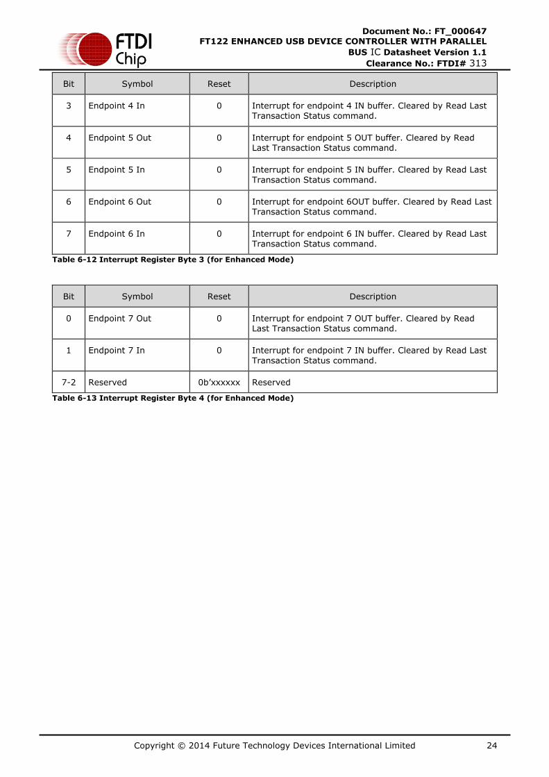
Copyright © 2014 Future Technology Devices International Limited 24
Document No.: FT_000647 FT122 ENHANCED USB DEVICE CONTROLLER WITH PARALLEL
BUS IC Datasheet Version 1.1
Clearance No.: FTDI# 313
Bit Symbol Reset Description
3 Endpoint 4 In 0 Interrupt for endpoint 4 IN buffer. Cleared by Read Last Transaction Status command.
4 Endpoint 5 Out 0 Interrupt for endpoint 5 OUT buffer. Cleared by Read Last Transaction Status command.
5 Endpoint 5 In 0 Interrupt for endpoint 5 IN buffer. Cleared by Read Last
Transaction Status command.
6 Endpoint 6 Out 0 Interrupt for endpoint 6OUT buffer. Cleared by Read Last Transaction Status command.
7 Endpoint 6 In 0 Interrupt for endpoint 6 IN buffer. Cleared by Read Last Transaction Status command.
Table 6-12 Interrupt Register Byte 3 (for Enhanced Mode)
Bit Symbol Reset Description
0 Endpoint 7 Out 0 Interrupt for endpoint 7 OUT buffer. Cleared by Read Last Transaction Status command.
1 Endpoint 7 In 0 Interrupt for endpoint 7 IN buffer. Cleared by Read Last
Transaction Status command.
7-2 Reserved 0b’xxxxxx Reserved
Table 6-13 Interrupt Register Byte 4 (for Enhanced Mode)
Copyright © 2014 Future Technology Devices International Limited 25
Document No.: FT_000647 FT122 ENHANCED USB DEVICE CONTROLLER WITH PARALLEL
BUS IC Datasheet Version 1.1
Clearance No.: FTDI# 313
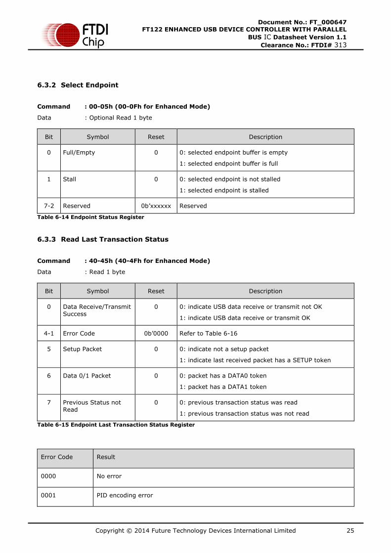
6.3.2 Select Endpoint
Command : 00-05h (00-0Fh for Enhanced Mode)
Data : Optional Read 1 byte
Bit Symbol Reset Description
0 Full/Empty 0 0: selected endpoint buffer is empty
1: selected endpoint buffer is full
1 Stall 0 0: selected endpoint is not stalled
1: selected endpoint is stalled
7-2 Reserved 0b’xxxxxx Reserved
Table 6-14 Endpoint Status Register
6.3.3 Read Last Transaction Status
Command : 40-45h (40-4Fh for Enhanced Mode)
Data : Read 1 byte
Bit Symbol Reset Description
0 Data Receive/Transmit
Success
0 0: indicate USB data receive or transmit not OK
1: indicate USB data receive or transmit OK
4-1 Error Code 0b’0000 Refer to Table 6-16
5 Setup Packet 0 0: indicate not a setup packet
1: indicate last received packet has a SETUP token
6 Data 0/1 Packet 0 0: packet has a DATA0 token
1: packet has a DATA1 token
7 Previous Status not Read
0 0: previous transaction status was read
1: previous transaction status was not read
Table 6-15 Endpoint Last Transaction Status Register
Error Code Result
0000 No error
0001 PID encoding error
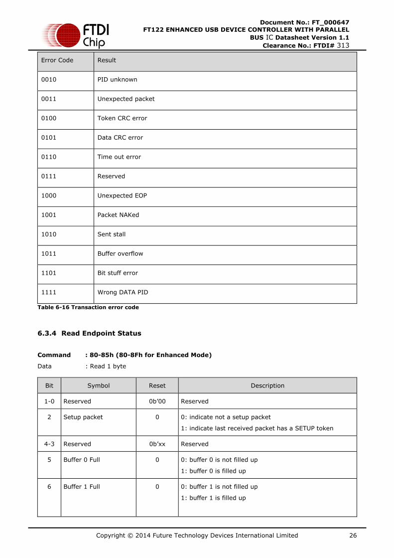
Copyright © 2014 Future Technology Devices International Limited 26
Document No.: FT_000647 FT122 ENHANCED USB DEVICE CONTROLLER WITH PARALLEL
BUS IC Datasheet Version 1.1
Clearance No.: FTDI# 313
Error Code Result
0010 PID unknown
0011 Unexpected packet
0100 Token CRC error
0101 Data CRC error
0110 Time out error
0111 Reserved
1000 Unexpected EOP
1001 Packet NAKed
1010 Sent stall
1011 Buffer overflow
1101 Bit stuff error
1111 Wrong DATA PID
Table 6-16 Transaction error code
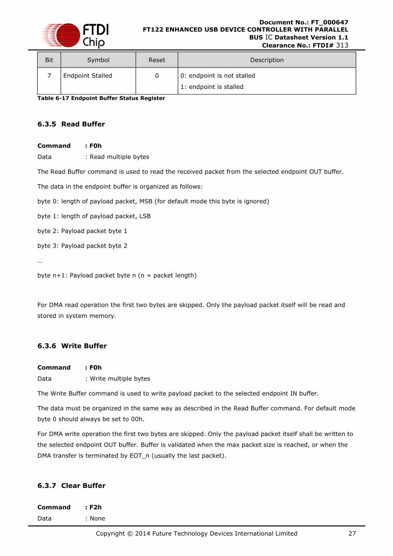
6.3.4 Read Endpoint Status
Command : 80-85h (80-8Fh for Enhanced Mode)
Data : Read 1 byte
Bit Symbol Reset Description
1-0 Reserved 0b’00 Reserved
2 Setup packet 0 0: indicate not a setup packet
1: indicate last received packet has a SETUP token
4-3 Reserved 0b’xx Reserved
5 Buffer 0 Full 0 0: buffer 0 is not filled up
1: buffer 0 is filled up
6 Buffer 1 Full 0 0: buffer 1 is not filled up
1: buffer 1 is filled up
Copyright © 2014 Future Technology Devices International Limited 27
Document No.: FT_000647 FT122 ENHANCED USB DEVICE CONTROLLER WITH PARALLEL
BUS IC Datasheet Version 1.1
Clearance No.: FTDI# 313
Bit Symbol Reset Description
7 Endpoint Stalled 0 0: endpoint is not stalled
1: endpoint is stalled
Table 6-17 Endpoint Buffer Status Register
6.3.5 Read Buffer
Command : F0h
Data : Read multiple bytes
The Read Buffer command is used to read the received packet from the selected endpoint OUT buffer.
The data in the endpoint buffer is organized as follows:
byte 0: length of payload packet, MSB (for default mode this byte is ignored)
byte 1: length of payload packet, LSB
byte 2: Payload packet byte 1
byte 3: Payload packet byte 2
…
byte n+1: Payload packet byte n (n = packet length)
For DMA read operation the first two bytes are skipped. Only the payload packet itself will be read and
stored in system memory.
6.3.6 Write Buffer
Command : F0h
Data : Write multiple bytes
The Write Buffer command is used to write payload packet to the selected endpoint IN buffer.
The data must be organized in the same way as described in the Read Buffer command. For default mode
byte 0 should always be set to 00h.
For DMA write operation the first two bytes are skipped. Only the payload packet itself shall be written to
the selected endpoint OUT buffer. Buffer is validated when the max packet size is reached, or when the
DMA transfer is terminated by EOT_n (usually the last packet).
6.3.7 Clear Buffer
Command : F2h
Data : None
Copyright © 2014 Future Technology Devices International Limited 28
Document No.: FT_000647 FT122 ENHANCED USB DEVICE CONTROLLER WITH PARALLEL
BUS IC Datasheet Version 1.1
Clearance No.: FTDI# 313
The Clear Buffer command should be issued after all data has been read out from the endpoint buffer.
This is to free the buffer to receive next packet from USB host.
6.3.8 Validate Buffer
Command : FAh
Data : None
The Validate Buffer command should be issued after all data has been written to the endpoint buffer. This
is to set the buffer full flag so that the packet can be sent to USB host when IN token arrives.
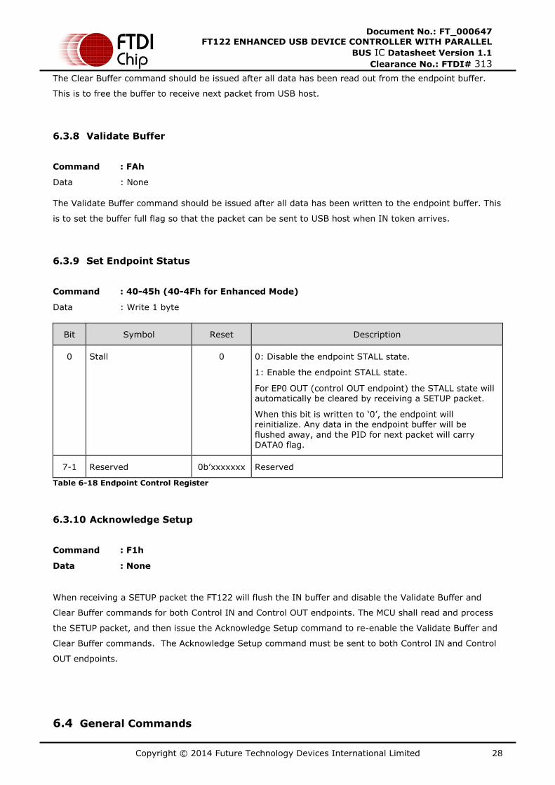
6.3.9 Set Endpoint Status
Command : 40-45h (40-4Fh for Enhanced Mode)
Data : Write 1 byte
Bit Symbol Reset Description
0 Stall 0 0: Disable the endpoint STALL state.
1: Enable the endpoint STALL state.
For EP0 OUT (control OUT endpoint) the STALL state will automatically be cleared by receiving a SETUP packet.
When this bit is written to ‘0’, the endpoint will reinitialize. Any data in the endpoint buffer will be flushed away, and the PID for next packet will carry
DATA0 flag.
7-1 Reserved 0b’xxxxxxx Reserved
Table 6-18 Endpoint Control Register
6.3.10 Acknowledge Setup
Command : F1h
Data : None
When receiving a SETUP packet the FT122 will flush the IN buffer and disable the Validate Buffer and
Clear Buffer commands for both Control IN and Control OUT endpoints. The MCU shall read and process
the SETUP packet, and then issue the Acknowledge Setup command to re-enable the Validate Buffer and
Clear Buffer commands. The Acknowledge Setup command must be sent to both Control IN and Control
OUT endpoints.
6.4 General Commands
Copyright © 2014 Future Technology Devices International Limited 29
Document No.: FT_000647 FT122 ENHANCED USB DEVICE CONTROLLER WITH PARALLEL
BUS IC Datasheet Version 1.1
Clearance No.: FTDI# 313
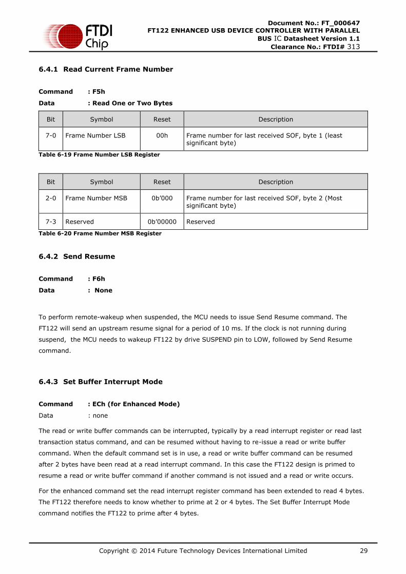
6.4.1 Read Current Frame Number
Command : F5h
Data : Read One or Two Bytes
Bit Symbol Reset Description
7-0 Frame Number LSB 00h Frame number for last received SOF, byte 1 (least significant byte)
Table 6-19 Frame Number LSB Register
Bit Symbol Reset Description
2-0 Frame Number MSB 0b’000 Frame number for last received SOF, byte 2 (Most significant byte)
7-3 Reserved 0b’00000 Reserved
Table 6-20 Frame Number MSB Register
6.4.2 Send Resume
Command : F6h
Data : None
To perform remote-wakeup when suspended, the MCU needs to issue Send Resume command. The
FT122 will send an upstream resume signal for a period of 10 ms. If the clock is not running during
suspend, the MCU needs to wakeup FT122 by drive SUSPEND pin to LOW, followed by Send Resume
command.
6.4.3 Set Buffer Interrupt Mode
Command : ECh (for Enhanced Mode)
Data : none
The read or write buffer commands can be interrupted, typically by a read interrupt register or read last
transaction status command, and can be resumed without having to re-issue a read or write buffer
command. When the default command set is in use, a read or write buffer command can be resumed
after 2 bytes have been read at a read interrupt command. In this case the FT122 design is primed to
resume a read or write buffer command if another command is not issued and a read or write occurs.
For the enhanced command set the read interrupt register command has been extended to read 4 bytes.
The FT122 therefore needs to know whether to prime at 2 or 4 bytes. The Set Buffer Interrupt Mode
command notifies the FT122 to prime after 4 bytes.
Copyright © 2014 Future Technology Devices International Limited 30
Document No.: FT_000647 FT122 ENHANCED USB DEVICE CONTROLLER WITH PARALLEL
BUS IC Datasheet Version 1.1
Clearance No.: FTDI# 313
6.4.4 Read Vendor ID
Command : EBh (for Enhanced Mode)
Data : read 2 bytes
Read the 2 bytes Vendor ID. Shall return 0403h.
6.4.5 Read Product ID
Command : EAh (for Enhanced Mode)
Data : read 2 bytes
Read the 2 bytes Product ID. Shall return 6018h.
6.4.6 Read FTDI ID
Command : EDh (for Enhanced Mode)
Data : read 1 byte
Read the 1 byte FTDI ID. Shall return 11h.
6.4.7 Set IO Pad Drive Strength
Command : E9h
Data : Write 1 byte
Bit Symbol Reset Description
1-0 CLKOUT pin 0b’00 00: 4mA
01: 8mA
10: 12mA
11:16mA
3-2 D[7:0] pins 0b’00 00: 4mA
01: 8mA
10: 12mA
11:16mA
5-4 INT_n, SUSPEND, DMREQ pins
0b’00 00: 4mA
01: 8mA
10: 12mA
11:16mA
7-6 GL_n pin 0b’00 00: 4mA
01: 8mA
10: 12mA
11:16mA

Copyright © 2014 Future Technology Devices International Limited 31
Document No.: FT_000647 FT122 ENHANCED USB DEVICE CONTROLLER WITH PARALLEL
BUS IC Datasheet Version 1.1
Clearance No.: FTDI# 313
Table 6-21 IO Pad Drive Strength Register
Copyright © 2014 Future Technology Devices International Limited 32
Document No.: FT_000647 FT122 ENHANCED USB DEVICE CONTROLLER WITH PARALLEL
BUS IC Datasheet Version 1.1
Clearance No.: FTDI# 313
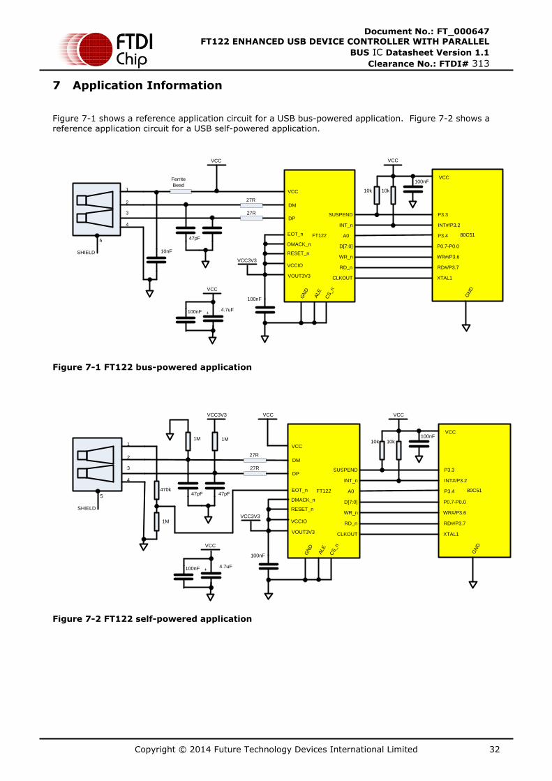
7 Application Information
Figure 7-1 shows a reference application circuit for a USB bus-powered application. Figure 7-2 shows a reference application circuit for a USB self-powered application.
FT122
1
2
3
4
5
SHIELD
Ferrite
Bead
VCC
VOUT3V3
DM
DP
VCCIO
VCC
CS
_n
RESET_n
100nF
10nF
27R
27R
80C51
VCC
VCC
GN
D
SUSPEND
CLKOUT
RD_n
WR_n
D[7:0]
A0
INT_n
DMACK_n
EOT_n
ALE
P3.3
XTAL1
RD#/P3.7
WR#/P3.6
P0.7-P0.0
P3.4
INT#/P3.2
GN
D
100nF
VCC3V3
47pF
100nF 4.7uF+
VCC
10k 10k
Figure 7-1 FT122 bus-powered application
FT122
VCC
VOUT3V3
DM
DP
VCCIO
CS
_n
RESET_n
100nF
27R
27R
80C51
VCC
VCC
GN
D
SUSPEND
CLKOUT
RD_n
WR_n
D[7:0]
A0
INT_n
DMACK_n
EOT_n
ALE
P3.3
XTAL1
RD#/P3.7
WR#/P3.6
P0.7-P0.0
P3.4
INT#/P3.2
GN
D
100nF
VCC3V3
1
2
3
4
5
SHIELD
470k
1M
47pF 47pF
VCC3V3
1M 1M
100nF 4.7uF+
VCC
VCC
10k 10k
Figure 7-2 FT122 self-powered application
Copyright © 2014 Future Technology Devices International Limited 33
Document No.: FT_000647 FT122 ENHANCED USB DEVICE CONTROLLER WITH PARALLEL
BUS IC Datasheet Version 1.1
Clearance No.: FTDI# 313
8 Devices Characteristics and Ratings
8.1 Absolute Maximum Ratings
The absolute maximum ratings for the FT122 devices are as follows. These are in accordance with the
Absolute Maximum Rating System (IEC 60134). Exceeding these may cause permanent damage to the
device.
Parameter Value Unit
Storage Temperature -65 to 150 °C
Floor Life (Out of Bag) At Factory Ambient
(30°C / 60% Relative Humidity)
168
(IPC/JEDEC J-STD-033A MSL Level 3
Compliant)*
Hours
Ambient Temperature (Power Applied) -40 to 85 °C
Latch-up current ±200 mA
Electrostatic Discharge Voltage(ESD)
human body model(HBM) ±2 kV
Electrostatic Discharge Voltage(ESD)
machine model(MM) ±200 V
Electrostatic Discharge Voltage(ESD)
charged device model(CDM) ±500 V
VCC Supply Voltage -0.5 to +6.0 V
DC Input Voltage – DP and USBDM -0.5 to +3.8 V
DC Input Voltage – High Impedance Bidirectional
-0.5 to + (VCC +0.5) V
DC Input Voltage – All Other Inputs -0.5 to + (VCC +0.5) V
DC Output Current – Outputs 22 mA
Table 8-1 Absolute Maximum Ratings
* If devices are stored out of the packaging beyond this time limit the devices should be baked before
use. The devices should be ramped up to a temperature of +125°C and baked for up to 17 hours.
Copyright © 2014 Future Technology Devices International Limited 34
Document No.: FT_000647 FT122 ENHANCED USB DEVICE CONTROLLER WITH PARALLEL
BUS IC Datasheet Version 1.1
Clearance No.: FTDI# 313
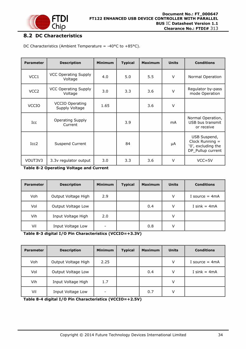
8.2 DC Characteristics
DC Characteristics (Ambient Temperature = -40°C to +85°C).
Parameter Description Minimum Typical Maximum Units Conditions
VCC1 VCC Operating Supply
Voltage 4.0 5.0 5.5 V Normal Operation
VCC2 VCC Operating Supply
Voltage 3.0 3.3 3.6 V
Regulator by-pass mode Operation
VCCIO VCCIO Operating Supply Voltage
1.65 3.6 V
Icc Operating Supply
Current 3.9 mA
Normal Operation, USB bus transmit
or receive
Icc2 Suspend Current 84 μA
USB Suspend, Clock Running =
‘0’, excluding the DP_Pullup current
VOUT3V3 3.3v regulator output 3.0 3.3 3.6 V VCC=5V
Table 8-2 Operating Voltage and Current
Parameter Description Minimum Typical Maximum Units Conditions
Voh Output Voltage High 2.9 V I source = 4mA
Vol Output Voltage Low 0.4 V I sink = 4mA
Vih Input Voltage High 2.0 V
Vil Input Voltage Low - 0.8 V
Table 8-3 digital I/O Pin Characteristics (VCCIO=+3.3V)
Parameter Description Minimum Typical Maximum Units Conditions
Voh Output Voltage High 2.25 V I source = 4mA
Vol Output Voltage Low 0.4 V I sink = 4mA
Vih Input Voltage High 1.7 V
Vil Input Voltage Low - 0.7 V
Table 8-4 digital I/O Pin Characteristics (VCCIO=+2.5V)
Copyright © 2014 Future Technology Devices International Limited 35
Document No.: FT_000647 FT122 ENHANCED USB DEVICE CONTROLLER WITH PARALLEL
BUS IC Datasheet Version 1.1
Clearance No.: FTDI# 313
Parameter Description Minimum Typical Maximum Units Conditions
Voh Output Voltage High 1.62 V I source = 4mA
Vol Output Voltage Low 0.4 V I sink = 4mA
Vih Input Voltage High 1.17 V
Vil Input Voltage Low - 0.63 V
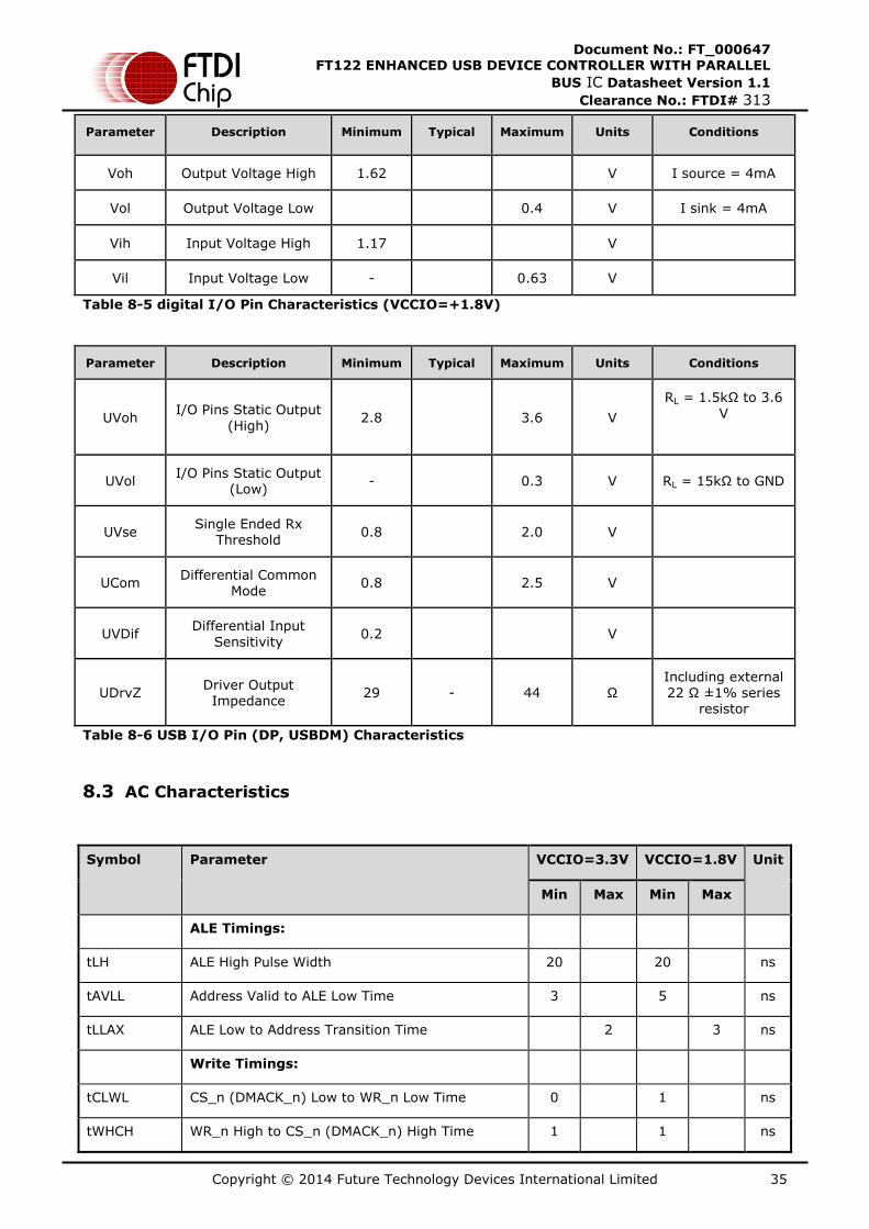
Table 8-5 digital I/O Pin Characteristics (VCCIO=+1.8V)
Parameter Description Minimum Typical Maximum Units Conditions
UVoh I/O Pins Static Output
(High) 2.8 3.6 V
RL = 1.5kΩ to 3.6
V
UVol I/O Pins Static Output
(Low) - 0.3 V RL = 15kΩ to GND
UVse Single Ended Rx
Threshold 0.8 2.0 V
UCom Differential Common
Mode 0.8 2.5 V
UVDif Differential Input
Sensitivity 0.2 V
UDrvZ Driver Output Impedance
29 - 44 Ω
Including external
22 Ω ±1% series resistor
Table 8-6 USB I/O Pin (DP, USBDM) Characteristics
8.3 AC Characteristics
Symbol Parameter VCCIO=3.3V VCCIO=1.8V Unit
Min Max Min Max
ALE Timings:
tLH ALE High Pulse Width 20 20 ns
tAVLL Address Valid to ALE Low Time 3 5 ns
tLLAX ALE Low to Address Transition Time 2 3 ns
Write Timings:
tCLWL CS_n (DMACK_n) Low to WR_n Low Time 0 1 ns
tWHCH WR_n High to CS_n (DMACK_n) High Time 1 1 ns
Copyright © 2014 Future Technology Devices International Limited 36
Document No.: FT_000647 FT122 ENHANCED USB DEVICE CONTROLLER WITH PARALLEL
BUS IC Datasheet Version 1.1
Clearance No.: FTDI# 313
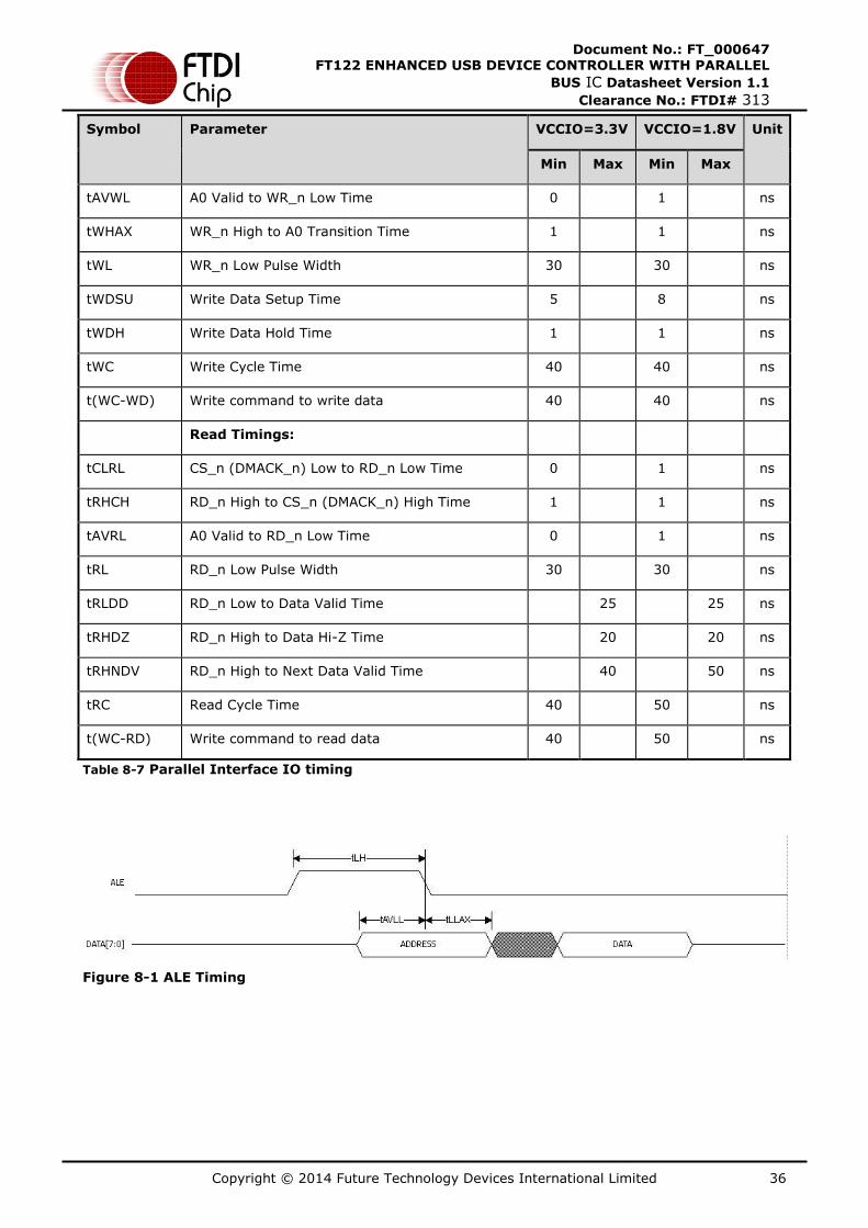
Symbol Parameter VCCIO=3.3V VCCIO=1.8V Unit
Min Max Min Max
tAVWL A0 Valid to WR_n Low Time 0 1 ns
tWHAX WR_n High to A0 Transition Time 1 1 ns
tWL WR_n Low Pulse Width 30 30 ns
tWDSU Write Data Setup Time 5 8 ns
tWDH Write Data Hold Time 1 1 ns
tWC Write Cycle Time 40 40 ns
t(WC-WD) Write command to write data 40 40 ns
Read Timings:
tCLRL CS_n (DMACK_n) Low to RD_n Low Time 0 1 ns
tRHCH RD_n High to CS_n (DMACK_n) High Time 1 1 ns
tAVRL A0 Valid to RD_n Low Time 0 1 ns
tRL RD_n Low Pulse Width 30 30 ns
tRLDD RD_n Low to Data Valid Time 25 25 ns
tRHDZ RD_n High to Data Hi-Z Time 20 20 ns
tRHNDV RD_n High to Next Data Valid Time 40 50 ns
tRC Read Cycle Time 40 50 ns
t(WC-RD) Write command to read data 40 50 ns
Table 8-7 Parallel Interface IO timing
Figure 8-1 ALE Timing
Copyright © 2014 Future Technology Devices International Limited 37
Document No.: FT_000647 FT122 ENHANCED USB DEVICE CONTROLLER WITH PARALLEL
BUS IC Datasheet Version 1.1
Clearance No.: FTDI# 313
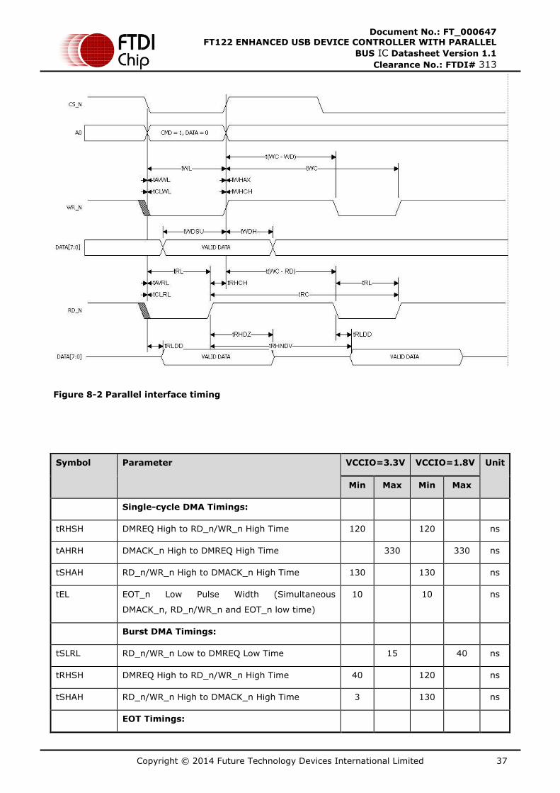
Figure 8-2 Parallel interface timing
Symbol Parameter VCCIO=3.3V VCCIO=1.8V Unit
Min Max Min Max
Single-cycle DMA Timings:
tRHSH DMREQ High to RD_n/WR_n High Time 120 120 ns
tAHRH DMACK_n High to DMREQ High Time 330 330 ns
tSHAH RD_n/WR_n High to DMACK_n High Time 130 130 ns
tEL EOT_n Low Pulse Width (Simultaneous
DMACK_n, RD_n/WR_n and EOT_n low time)
10 10 ns
Burst DMA Timings:
tSLRL RD_n/WR_n Low to DMREQ Low Time 15 40 ns
tRHSH DMREQ High to RD_n/WR_n High Time 40 120 ns
tSHAH RD_n/WR_n High to DMACK_n High Time 3 130 ns
EOT Timings:
Copyright © 2014 Future Technology Devices International Limited 38
Document No.: FT_000647 FT122 ENHANCED USB DEVICE CONTROLLER WITH PARALLEL
BUS IC Datasheet Version 1.1
Clearance No.: FTDI# 313
Symbol Parameter VCCIO=3.3V VCCIO=1.8V Unit
Min Max Min Max
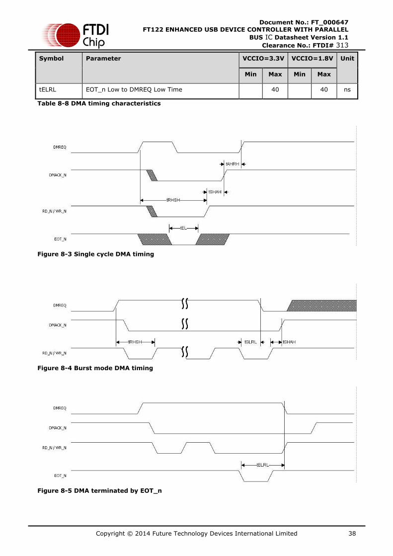
tELRL EOT_n Low to DMREQ Low Time 40 40 ns
Table 8-8 DMA timing characteristics
Figure 8-3 Single cycle DMA timing
Figure 8-4 Burst mode DMA timing
Figure 8-5 DMA terminated by EOT_n
Copyright © 2014 Future Technology Devices International Limited 39
Document No.: FT_000647 FT122 ENHANCED USB DEVICE CONTROLLER WITH PARALLEL
BUS IC Datasheet Version 1.1
Clearance No.: FTDI# 313
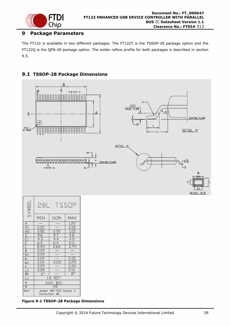
9 Package Parameters
The FT122 is available in two different packages. The FT122T is the TSSOP-28 package option and the
FT122Q is the QFN-28 package option. The solder reflow profile for both packages is described in section
9.5.
9.1 TSSOP-28 Package Dimensions
Figure 9-1 TSSOP-28 Package Dimensions
Copyright © 2014 Future Technology Devices International Limited 40
Document No.: FT_000647 FT122 ENHANCED USB DEVICE CONTROLLER WITH PARALLEL
BUS IC Datasheet Version 1.1
Clearance No.: FTDI# 313
The FT122T is supplied in a RoHS compliant 28 pin TSSOP package. The package is lead (Pb) free and
uses a ‘green’ compound. The package is fully compliant with European Union directive 2002/95/EC.
This package is nominally 4.4mm x 9.7mm body (6.4mm x9.7mm including pins). The pins are on a 0.65
mm pitch. The above mechanical drawing shows the TSSOP-28 package.
All dimensions are in millimetres.
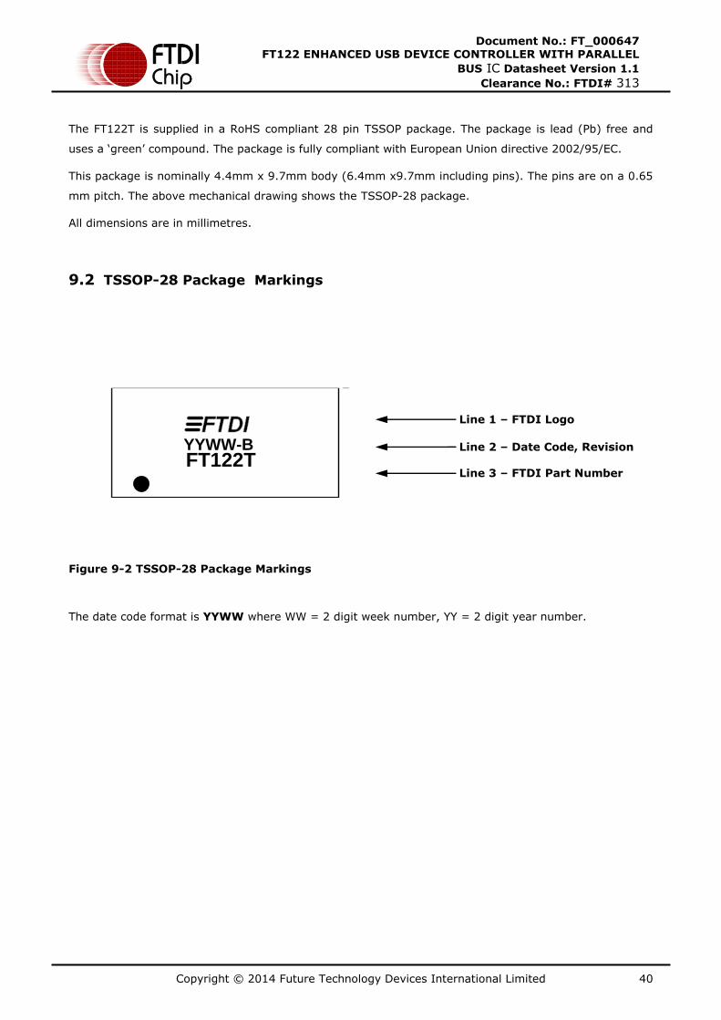
9.2 TSSOP-28 Package Markings
Figure 9-2 TSSOP-28 Package Markings
The date code format is YYWW where WW = 2 digit week number, YY = 2 digit year number.
Line 1 – FTDI Logo
Line 2 – Date Code, Revision
Line 3 – FTDI Part Number FT122TYYWW-B
Copyright © 2014 Future Technology Devices International Limited 41
Document No.: FT_000647 FT122 ENHANCED USB DEVICE CONTROLLER WITH PARALLEL
BUS IC Datasheet Version 1.1
Clearance No.: FTDI# 313
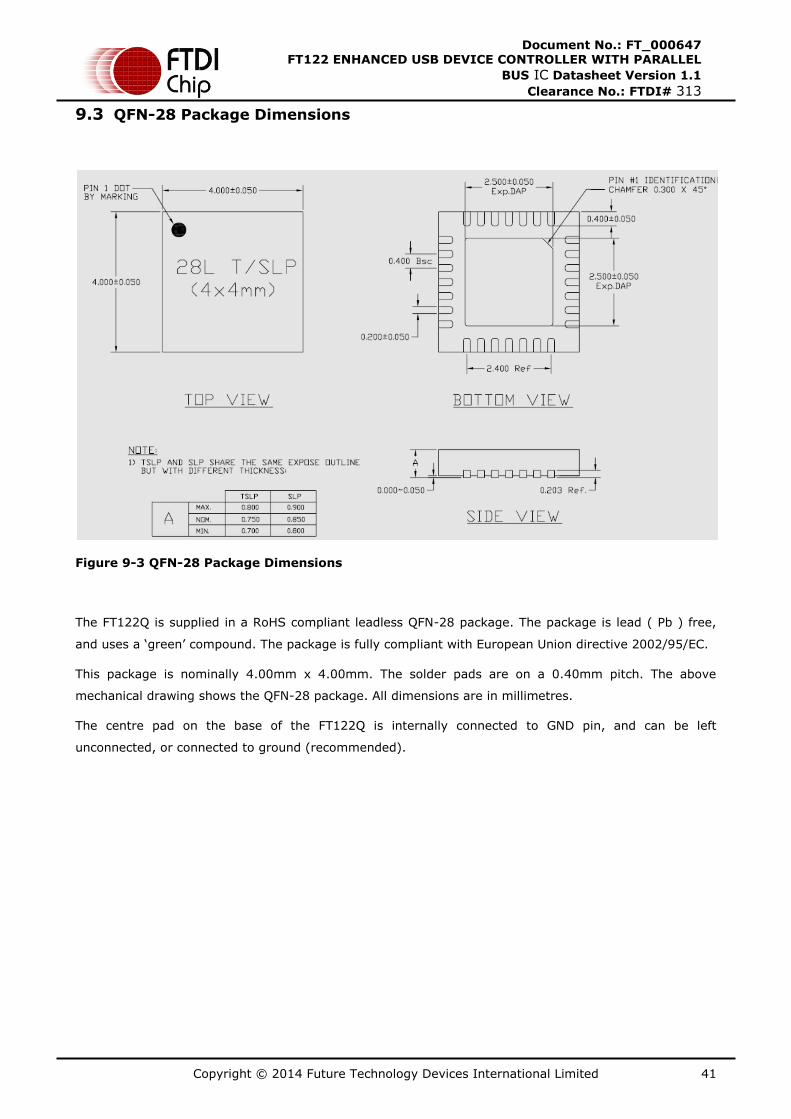
9.3 QFN-28 Package Dimensions
Figure 9-3 QFN-28 Package Dimensions
The FT122Q is supplied in a RoHS compliant leadless QFN-28 package. The package is lead ( Pb ) free,
and uses a ‘green’ compound. The package is fully compliant with European Union directive 2002/95/EC.
This package is nominally 4.00mm x 4.00mm. The solder pads are on a 0.40mm pitch. The above
mechanical drawing shows the QFN-28 package. All dimensions are in millimetres.
The centre pad on the base of the FT122Q is internally connected to GND pin, and can be left
unconnected, or connected to ground (recommended).
Copyright © 2014 Future Technology Devices International Limited 42
Document No.: FT_000647 FT122 ENHANCED USB DEVICE CONTROLLER WITH PARALLEL
BUS IC Datasheet Version 1.1
Clearance No.: FTDI# 313
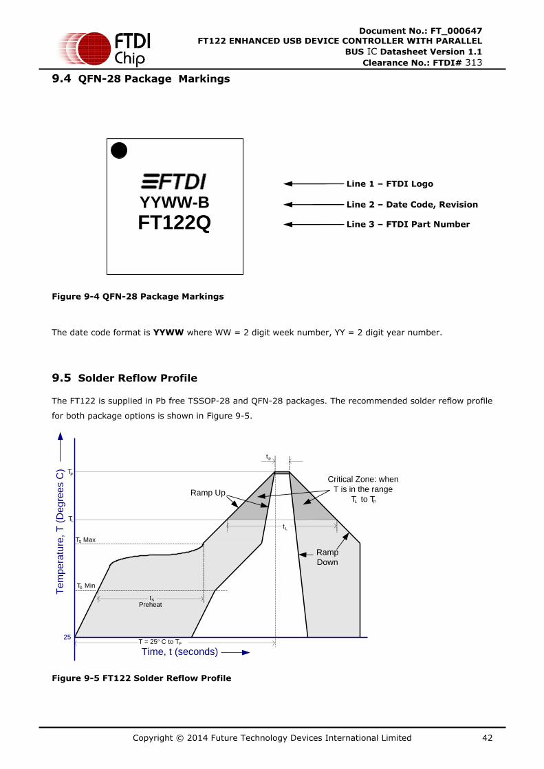
9.4 QFN-28 Package Markings
Figure 9-4 QFN-28 Package Markings
The date code format is YYWW where WW = 2 digit week number, YY = 2 digit year number.
9.5 Solder Reflow Profile
The FT122 is supplied in Pb free TSSOP-28 and QFN-28 packages. The recommended solder reflow profile
for both package options is shown in Figure 9-5.
Figure 9-5 FT122 Solder Reflow Profile
Critical Zone: when
T is in the range
T to T
Te
mpera
ture
, T
(D
eg
ree
s C
)
Time, t (seconds)
25PT = 25º C to T
tp
Tp
TL
tPreheat
S
tL
Ramp UpL p
Ramp
Down
T MaxS
T MinS
Line 1 – FTDI Logo
Line 2 – Date Code, Revision
Line 3 – FTDI Part Number FT122QYYWW-B
Copyright © 2014 Future Technology Devices International Limited 43
Document No.: FT_000647 FT122 ENHANCED USB DEVICE CONTROLLER WITH PARALLEL
BUS IC Datasheet Version 1.1
Clearance No.: FTDI# 313
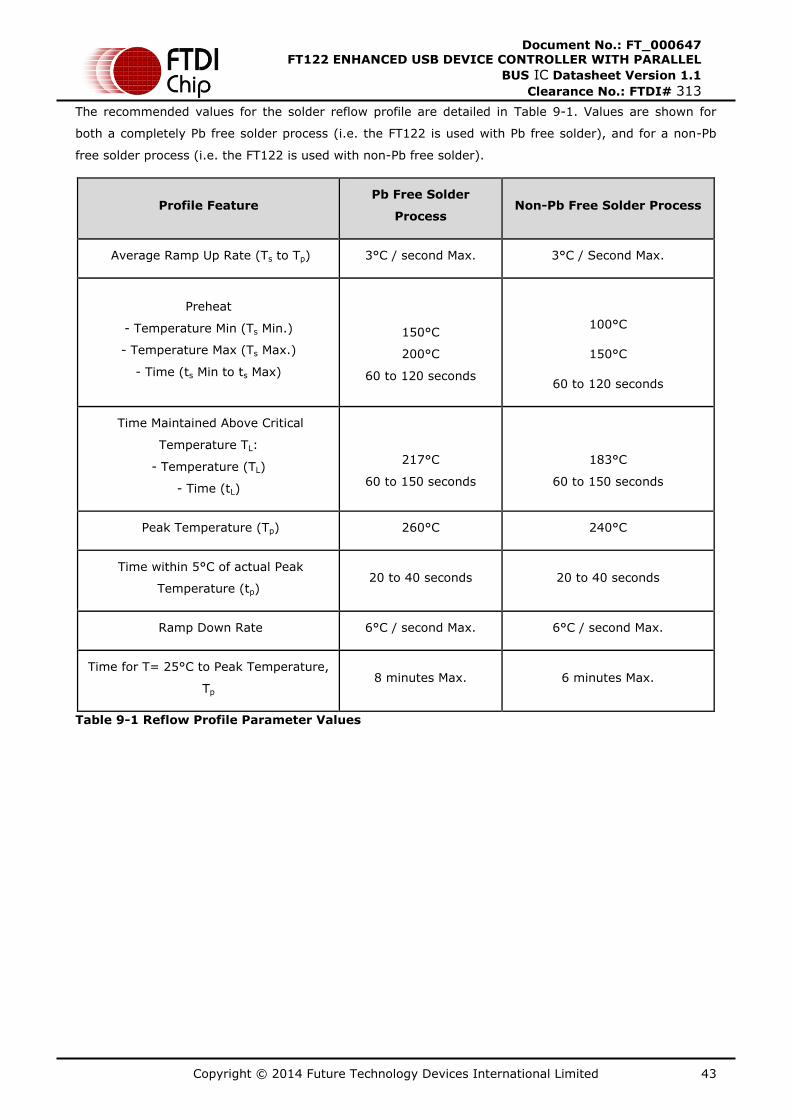
The recommended values for the solder reflow profile are detailed in Table 9-1. Values are shown for
both a completely Pb free solder process (i.e. the FT122 is used with Pb free solder), and for a non-Pb
free solder process (i.e. the FT122 is used with non-Pb free solder).
Profile Feature Pb Free Solder
Process Non-Pb Free Solder Process
Average Ramp Up Rate (Ts to Tp) 3°C / second Max. 3°C / Second Max.
Preheat
- Temperature Min (Ts Min.)
- Temperature Max (Ts Max.)
- Time (ts Min to ts Max)
150°C
200°C
60 to 120 seconds
100°C
150°C
60 to 120 seconds
Time Maintained Above Critical
Temperature TL:
- Temperature (TL)
- Time (tL)
217°C
60 to 150 seconds
183°C
60 to 150 seconds
Peak Temperature (Tp) 260°C 240°C
Time within 5°C of actual Peak
Temperature (tp) 20 to 40 seconds 20 to 40 seconds
Ramp Down Rate 6°C / second Max. 6°C / second Max.
Time for T= 25°C to Peak Temperature,
Tp 8 minutes Max. 6 minutes Max.
Table 9-1 Reflow Profile Parameter Values
Copyright © 2014 Future Technology Devices International Limited 44
Document No.: FT_000647 FT122 ENHANCED USB DEVICE CONTROLLER WITH PARALLEL
BUS IC Datasheet Version 1.1
Clearance No.: FTDI# 313
10 Contact Information
Head Office – Glasgow, UK Future Technology Devices International Limited Unit 1, 2 Seaward Place, Centurion Business Park Glasgow G41 1HH United Kingdom Tel: +44 (0) 141 429 2777 Fax: +44 (0) 141 429 2758 E-mail (Sales) [email protected] E-mail (Support) [email protected] E-mail (General Enquiries) [email protected]
Branch Office – Taipei, Taiwan Future Technology Devices International Limited (Taiwan) 2F, No. 516, Sec. 1, NeiHu Road Taipei 114 Taiwan , R.O.C. Tel: +886 (0) 2 8791 3570 Fax: +886 (0) 2 8791 3576 E-mail (Sales) [email protected] E-mail (Support) [email protected] E-mail (General Enquiries) [email protected]
Branch Office – Tigard, Oregon, USA Future Technology Devices International Limited (USA) 7130 SW Fir Loop Tigard, OR 97223 Tel: +1 (503) 547 0988 Fax: +1 (503) 547 0987 E-Mail (Sales) [email protected] E-Mail (Support) [email protected]
E-Mail (General Enquiries) [email protected]
Branch Office – Shanghai, China Future Technology Devices International Limited (China) Room 1103, No.666 West Huaihai Road, Shanghai, 200052 China Tel: +86 21 62351596 Fax: +86 21 62351595 E-mail (Sales) [email protected] E-mail (Support) [email protected] E-mail (General Enquiries) [email protected]
Branch Office – Singapore Future Technology Devices International Limited (Singapore) 178 Paya Lebar Road #07-03/04/05 Singapore 409030 Tel: +65 6841 1174 Fax: +65 6841 6071 E-mail (Support) [email protected] E-mail (General Enquiries) [email protected]
Web Site http://ftdichip.com
System and equipment manufacturers and designers are responsible to ensure that their systems, and any Future
Technology Devices International Ltd (FTDI) devices incorporated in their systems, meet all applicable safety, regulatory
and system-level performance requirements. All application-related information in this document (including application
descriptions, suggested FTDI devices and other materials) is provided for reference only. While FTDI has taken care to
assure it is accurate, this information is subject to customer confirmation, and FTDI disclaims all liability for system designs
and for any applications assistance provided by FTDI. Use of FTDI devices in life support and/or safety applications is entirely at the user’s risk, and the user agrees to defend, indemnify and hold harmless FTDI from any and all damages,
claims, suits or expense resulting from such use. This document is subject to change without notice. No freedom to use
patents or other intellectual property rights is implied by the publication of this document. Neither the whole nor any part of
the information contained in, or the product described in this document, may be adapted or reproduced in any material or
electronic form without the prior written consent of the copyright holder. Future Technology Devices International Ltd, Unit
1, 2 Seaward Place, Centurion Business Park, Glasgow G41 1HH, United Kingdom. Scotland Registered Company Number:
SC136640
Copyright © 2014 Future Technology Devices International Limited 45
Document No.: FT_000647 FT122 ENHANCED USB DEVICE CONTROLLER WITH PARALLEL
BUS IC Datasheet Version 1.1
Clearance No.: FTDI# 313
Appendix A– References
Useful Application Notes
http://www.ftdichip.com/Documents/AppNotes/AN_167_FT1248_Parallel_Serial_Interface_Basics.pdf
http://www.ftdichip.com/Support/Documents/TechnicalNotes/TN_100_USB_VID-PID_Guidelines.pdf
http://www.ftdichip.com/Support/Documents/AppNotes/AN_175_Battery%20Charging%20Over%20USB%20with%20FTEX%20Devices.pdf
http://www.usb.org/developers/devclass_docs/BCv1.2_011912.zip
Appendix B - List of Figures and Tables
List of Figures
Figure 2-1 FT122 Block Diagram ..................................................................................................... 3
Figure 3-1 TSSOP-28 package schematic symbol .............................................................................. 6
Figure 3-2 QFN-28 package schematic symbol.................................................................................. 6
Figure 7-1 FT122 bus-powered application ..................................................................................... 32
Figure 7-2 FT122 self-powered application ..................................................................................... 32
Figure 8-1 ALE Timing ................................................................................................................. 36
Figure 8-2 Parallel interface timing ............................................................................................... 37
Figure 8-3 Single cycle DMA timing ............................................................................................... 38
Figure 8-4 Burst mode DMA timing ............................................................................................... 38
Figure 8-5 DMA terminated by EOT_n ........................................................................................... 38
Figure 9-1 TSSOP-28 Package Dimensions ..................................................................................... 39
Figure 9-2 TSSOP-28 Package Markings ........................................................................................ 40
Figure 9-3 QFN-28 Package Dimensions ........................................................................................ 41
Figure 9-4 QFN-28 Package Markings ............................................................................................ 42
Figure 9-5 FT122 Solder Reflow Profile .......................................................................................... 42
List of Tables
Table 3-1 FT122 Pin Description ..................................................................................................... 8
Table 4-1 Interrupt modes ........................................................................................................... 10
Table 5-1 Endpoint configuration for EP0 and EP1 ........................................................................... 11
Table 5-2 Endpoint configuration for EP2 ....................................................................................... 11
Table 5-3 - Example buffer configuration ....................................................................................... 12
Table 5-4 - Endpoint Maximum Packet Size .................................................................................... 13
Table 6-1 FT122 default command set ........................................................................................... 15
Table 6-2 enhanced command set ................................................................................................ 19
Table 6-3 Address Enable Register ................................................................................................ 19
Table 6-4 Endpoint Enable Register ............................................................................................... 19
Table 6-5 Configuration Register (Byte 1) ...................................................................................... 20
Table 6-6 Clock Division Factor Register (Byte 2) ............................................................................ 21
Table 6-7 DMA Configuration Register (Byte 1) ............................................................................... 22
Table 6-8 DMA Endpoint Select Register (Byte 2, for Enhanced Mode) ............................................... 22
Copyright © 2014 Future Technology Devices International Limited 46
Document No.: FT_000647 FT122 ENHANCED USB DEVICE CONTROLLER WITH PARALLEL
BUS IC Datasheet Version 1.1
Clearance No.: FTDI# 313
Table 6-9 Endpoint Configuration Register ..................................................................................... 22
Table 6-10 Interrupt Register Byte 1 ............................................................................................. 23
Table 6-11 Interrupt Register Byte 2 ............................................................................................. 23
Table 6-12 Interrupt Register Byte 3 (for Enhanced Mode) ............................................................... 24
Table 6-13 Interrupt Register Byte 4 (for Enhanced Mode) ............................................................... 24
Table 6-14 Endpoint Status Register ............................................................................................. 25
Table 6-15 Endpoint Last Transaction Status Register ..................................................................... 25
Table 6-16 Transaction error code ................................................................................................ 26
Table 6-17 Endpoint Buffer Status Register .................................................................................... 27
Table 6-18 Endpoint Control Register ............................................................................................ 28
Table 6-19 Frame Number LSB Register ........................................................................................ 29
Table 6-20 Frame Number MSB Register ........................................................................................ 29
Table 6-21 IO Pad Drive Strength Register ..................................................................................... 31
Table 8-1 Absolute Maximum Ratings ............................................................................................ 33
Table 8-2 Operating Voltage and Current ....................................................................................... 34
Table 8-3 digital I/O Pin Characteristics (VCCIO=+3.3V) ................................................................. 34
Table 8-4 digital I/O Pin Characteristics (VCCIO=+2.5V) ................................................................. 34
Table 8-5 digital I/O Pin Characteristics (VCCIO=+1.8V) ................................................................. 35
Table 8-6 USB I/O Pin (DP, USBDM) Characteristics ........................................................................ 35
Table 8-7 Parallel Interface IO timing ............................................................................................ 36
Table 8-8 DMA timing characteristics ............................................................................................. 38
Table 9-1 Reflow Profile Parameter Values ..................................................................................... 43
Copyright © 2014 Future Technology Devices International Limited 47
Document No.: FT_000647 FT122 ENHANCED USB DEVICE CONTROLLER WITH PARALLEL
BUS IC Datasheet Version 1.1
Clearance No.: FTDI# 313
Appendix C - Revision History
Document Title: DS_FT122
Document Reference No.: FT_000647
Clearance No.: FTDI# 133
Product Page: http://www.ftdichip.com/Products/ICs/FT122.htm
Document Feedback: Send Feedback
Version Draft Initial draft 30th July 2012
Version 1.0 Initial release 1st October 2012
Version 1.1 Updated release 23rd March 2015
Related Documents