E.1 Introduction E-2 E.2 Signal Processing and Embedded Applications: The Digital Signal Processor E-5 E.3 Embedded Benchmarks E-12 E.4 Embedded Multiprocessors E-14 E.5 Case Study: The Emotion Engine of the Sony PlayStation 2 E-15 E.6 Case Study: Sanyo VPC-SX500 Digital Camera E-19 E.7 Case Study: Inside a Cell Phone E-20 E.8 Concluding Remarks E-25

Welcome message from author
This document is posted to help you gain knowledge. Please leave a comment to let me know what you think about it! Share it to your friends and learn new things together.
Transcript
E.1 Introduction E-2
E.2 Signal Processing and Embedded Applications: The Digital Signal Processor E-5
E.3 Embedded Benchmarks E-12
E.4 Embedded Multiprocessors E-14
E.5 Case Study: The Emotion Engine of the Sony PlayStation 2 E-15
E.6 Case Study: Sanyo VPC-SX500 Digital Camera E-19
E.7 Case Study: Inside a Cell Phone E-20
E.8 Concluding Remarks E-25
EEmbedded Systems 1
By Thomas M. ConteNorth Carolina State University
Where a calculator on the ENIAC is equipped with 18,000 vacuum tubes and weighs 30 tons, computers in the future may have only 1,000 vacuum tubes and perhaps weigh 1 1/2 tons.
Popular MechanicsMarch 1949
E-2 ■ Appendix E Embedded Systems
Embedded computer systems—computers lodged in other devices where thepresence of the computers is not immediately obvious—are the fastest-growingportion of the computer market. These devices range from everyday machines(most microwaves, most washing machines, printers, network switches, and auto-mobiles contain simple to very advanced embedded microprocessors) to hand-held digital devices (such as PDAs, cell phones, and music players) to videogame consoles and digital set-top boxes. Although in some applications (such asPDAs) the computers are programmable, in many embedded applications theonly programming occurs in connection with the initial loading of the applicationcode or a later software upgrade of that application. Thus, the application is care-fully tuned for the processor and system. This process sometimes includes lim-ited use of assembly language in key loops, although time-to-market pressuresand good software engineering practice restrict such assembly language codingto a fraction of the application.
Compared to desktop and server systems, embedded systems have a muchwider range of processing power and cost—from systems containing low-end8-bit and 16-bit processors that may cost less than a dollar, to those containingfull 32-bit microprocessors capable of operating in the 500 MIPS range thatcost approximately 10 dollars, to those containing high-end embedded proces-sors that cost hundreds of dollars and can execute several billions of instruc-tions per second. Although the range of computing power in the embeddedsystems market is very large, price is a key factor in the design of computers forthis space. Performance requirements do exist, of course, but the primary goalis often meeting the performance need at a minimum price, rather than achiev-ing higher performance at a higher price.
Embedded systems often process information in very different ways fromgeneral-purpose processors. Typically these applications include deadline-drivenconstraints—so-called real-time constraints. In these applications, a particularcomputation must be completed by a certain time or the system fails (there areother constraints considered real time, discussed in the next subsection).
Embedded systems applications typically involve processing information assignals. The lay term “signal” often connotes radio transmission, and that is truefor some embedded systems (e.g., cell phones). But a signal may be an image, amotion picture composed of a series of images, a control sensor measurement,and so on. Signal processing requires specific computation that many embeddedprocessors are optimized for. We discuss this in depth below. A wide range ofbenchmark requirements exist, from the ability to run small, limited code seg-ments to the ability to perform well on applications involving tens to hundreds ofthousands of lines of code.
Two other key characteristics exist in many embedded applications: the needto minimize memory and the need to minimize power. In many embedded appli-cations, the memory can be a substantial portion of the system cost, and it isimportant to optimize memory size in such cases. Sometimes the application is
E.1 Introduction
E.1 Introduction ■ E-3
expected to fit entirely in the memory on the processor chip; other times theapplication needs to fit in its entirety in a small, off-chip memory. In either case,the importance of memory size translates to an emphasis on code size, since datasize is dictated by the application. Some architectures have special instruction setcapabilities to reduce code size. Larger memories also mean more power, andoptimizing power is often critical in embedded applications. Although theemphasis on low power is frequently driven by the use of batteries, the need touse less expensive packaging (plastic versus ceramic) and the absence of a fan forcooling also limit total power consumption. We examine the issue of power inmore detail later in this appendix.
Another important trend in embedded systems is the use of processor corestogether with application-specific circuitry—so-called “core plus ASIC” or “sys-tem on a chip” (SOC), which may also be viewed as special-purpose multipro-cessors (see Section E.4). Often an application’s functional and performancerequirements are met by combining a custom hardware solution together withsoftware running on a standardized embedded processor core, which is designedto interface to such special-purpose hardware. In practice, embedded problemsare usually solved by one of three approaches:
1. The designer uses a combined hardware/software solution that includes somecustom hardware and an embedded processor core that is integrated with thecustom hardware, often on the same chip.
2. The designer uses custom software running on an off-the-shelf embeddedprocessor.
3. The designer uses a digital signal processor and custom software for the pro-cessor. Digital signal processors are processors specially tailored for signal-processing applications. We discuss some of the important differencesbetween digital signal processors and general-purpose embedded processorsbelow.
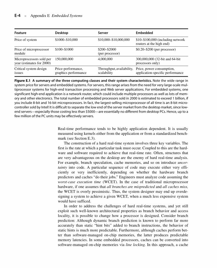
Figure E.1 summarizes these three classes of computing environments andtheir important characteristics.
Real-Time Processing
Often, the performance requirement in an embedded application is a real-timerequirement. A real-time performance requirement is one where a segment of theapplication has an absolute maximum execution time that is allowed. For exam-ple, in a digital set-top box the time to process each video frame is limited, sincethe processor must accept and process the frame before the next frame arrives(typically called hard real-time systems). In some applications, a more sophisti-cated requirement exists: The average time for a particular task is constrained aswell as is the number of instances when some maximum time is exceeded. Suchapproaches (typically called soft real-time) arise when it is possible to occasion-ally miss the time constraint on an event, as long as not too many are missed.
E-4 ■ Appendix E Embedded Systems
Real-time performance tends to be highly application dependent. It is usuallymeasured using kernels either from the application or from a standardized bench-mark (see Section E.3).
The construction of a hard real-time system involves three key variables. Thefirst is the rate at which a particular task must occur. Coupled to this are the hard-ware and software required to achieve that real-time rate. Often, structures thatare very advantageous on the desktop are the enemy of hard real-time analysis.For example, branch speculation, cache memories, and so on introduce uncer-tainty into code. A particular sequence of code may execute either very effi-ciently or very inefficiently, depending on whether the hardware branchpredictors and caches “do their jobs.” Engineers must analyze code assuming theworst-case execution time (WCET). In the case of traditional microprocessorhardware, if one assumes that all branches are mispredicted and all caches miss,the WCET is overly pessimistic. Thus, the system designer may end up overde-signing a system to achieve a given WCET, when a much less expensive systemwould have sufficed.
In order to address the challenges of hard real-time systems, and yet stillexploit such well-known architectural properties as branch behavior and accesslocality, it is possible to change how a processor is designed. Consider branchprediction: Although dynamic branch prediction is known to perform far moreaccurately than static “hint bits” added to branch instructions, the behavior ofstatic hints is much more predictable. Furthermore, although caches perform bet-ter than software-managed on-chip memories, the latter produces predictablememory latencies. In some embedded processors, caches can be converted intosoftware-managed on-chip memories via line locking. In this approach, a cache
Feature Desktop Server Embedded
Price of system $1000–$10,000 $10,000–$10,000,000 $10–$100,000 (including network routers at the high end)
Price of microprocessor module
$100–$1000 $200–$2000 (per processor)
$0.20–$200 (per processor)
Microprocessors sold per year (estimates for 2000)
150,000,000 4,000,000 300,000,000 (32-bit and 64-bit processors only)
Critical system design issues
Price-performance, graphics performance
Throughput, availability, scalability
Price, power consumption, application-specific performance
Figure E.1 A summary of the three computing classes and their system characteristics. Note the wide range insystem price for servers and embedded systems. For servers, this range arises from the need for very large-scale mul-tiprocessor systems for high-end transaction processing and Web server applications. For embedded systems, onesignificant high-end application is a network router, which could include multiple processors as well as lots of mem-ory and other electronics. The total number of embedded processors sold in 2000 is estimated to exceed 1 billion, ifyou include 8-bit and 16-bit microprocessors. In fact, the largest-selling microprocessor of all time is an 8-bit micro-controller sold by Intel! It is difficult to separate the low end of the server market from the desktop market, since low-end servers—especially those costing less than $5000—are essentially no different from desktop PCs. Hence, up to afew million of the PC units may be effectively servers.
E.2 Signal Processing and Embedded Applications: The Digital Signal Processor ■ E-5
line can be locked in the cache so that it cannot be replaced until the line isunlocked
A digital signal processor (DSP) is a special-purpose processor optimized forexecuting digital signal processing algorithms. Most of these algorithms, fromtime-domain filtering (e.g., infinite impulse response and finite impulse responsefiltering), to convolution, to transforms (e.g., fast Fourier transform, discretecosine transform), to even forward error correction (FEC) encodings, all have astheir kernel the same operation: a multiply-accumulate operation. For example,the discrete Fourier transform has the form:
where
The discrete cosine transform is often a replacement for this because it does notrequire complex number operations. Either transform has as its core the sum of aproduct. To accelerate this, DSPs typically feature special-purpose hardware toperform multiply-accumulate (MAC). A MAC instruction of “MAC A,B,C” hasthe semantics of “A = A + B * C.” In some situations, the performance of thisoperation is so critical that a DSP is selected for an application based solely uponits MAC operation throughput.
DSPs often employ fixed-point arithmetic. If you think of integers as having abinary point to the right of the least-significant bit, fixed point has a binary pointjust to the right of the sign bit. Hence, fixed-point data are fractions between –1and +1.
Example Here are three simple 16-bit patterns:
0100 0000 0000 0000
0000 1000 0000 0000
0100 1000 0000 1000
What values do they represent if they are two’s complement integers? Fixed-point numbers?
Answer Number representation tells us that the ith digit to the left of the binary point rep-resents 2i–1 and the ith digit to the right of the binary point represents 2–i. Firstassume these three patterns are integers. Then the binary point is to the far right,so they represent 214, 211, and (214+ 211+ 23), or 16,384, 2048, and 18,440.
Fixed point places the binary point just to the right of the sign bit, so asfixed point these patterns represent 2–1, 2–4, and (2–1+ 2–4 + 2–12). The fractions
E.2 Signal Processing and Embedded Applications: The Digital Signal Processor
X k( ) x n( )WNkn
n 0=
N 1–
∑= WNkn
ej2πkn
N-------------
2πknN------⎝ ⎠
⎛ ⎞ jsin 2πknN------⎝ ⎠
⎛ ⎞+cos= =
.
E-6 ■ Appendix E Embedded Systems
are 1/2, 1/16, and (2048 + 256 + 1)/4096 or 2305/4096, which represents about0.50000, 0.06250, and 0.56274. Alternatively, for an n-bit two’s complement,fixed-point number we could just divide the integer presentation by 2n–1 toderive the same results:
16,384/32,768 = 1/2, 2048/32,768 = 1/16, and 18,440/32,768 = 2305/4096.
Fixed point can be thought of as a low-cost floating point. It doesn’t includean exponent in every word and doesn’t have hardware that automatically alignsand normalizes operands. Instead, fixed point relies on the DSP programmer tokeep the exponent in a separate variable and ensure that each result is shifted leftor right to keep the answer aligned to that variable. Since this exponent variableis often shared by a set of fixed-point variables, this style of arithmetic is alsocalled blocked floating point, since a block of variables has a common exponent.
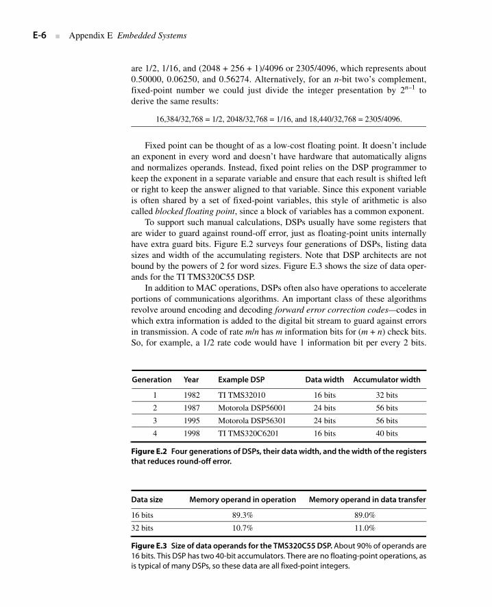
To support such manual calculations, DSPs usually have some registers thatare wider to guard against round-off error, just as floating-point units internallyhave extra guard bits. Figure E.2 surveys four generations of DSPs, listing datasizes and width of the accumulating registers. Note that DSP architects are notbound by the powers of 2 for word sizes. Figure E.3 shows the size of data oper-ands for the TI TMS320C55 DSP.
In addition to MAC operations, DSPs often also have operations to accelerateportions of communications algorithms. An important class of these algorithmsrevolve around encoding and decoding forward error correction codes—codes inwhich extra information is added to the digital bit stream to guard against errorsin transmission. A code of rate m/n has m information bits for (m + n) check bits.So, for example, a 1/2 rate code would have 1 information bit per every 2 bits.
Generation Year Example DSP Data width Accumulator width
1 1982 TI TMS32010 16 bits 32 bits
2 1987 Motorola DSP56001 24 bits 56 bits
3 1995 Motorola DSP56301 24 bits 56 bits
4 1998 TI TMS320C6201 16 bits 40 bits
Figure E.2 Four generations of DSPs, their data width, and the width of the registersthat reduces round-off error.
Data size Memory operand in operation Memory operand in data transfer
16 bits 89.3% 89.0%
32 bits 10.7% 11.0%
Figure E.3 Size of data operands for the TMS320C55 DSP. About 90% of operands are16 bits. This DSP has two 40-bit accumulators. There are no floating-point operations, asis typical of many DSPs, so these data are all fixed-point integers.
E.2 Signal Processing and Embedded Applications: The Digital Signal Processor ■ E-7
Such codes are often called trellis codes because one popular graphical flow dia-gram of their encoding resembles a garden trellis. A common algorithm fordecoding trellis codes is due to Viterbi. This algorithm requires a sequence ofcompares and selects in order to recover a transmitted bit’s true value. Thus DSPsoften have compare-select operations to support Viterbi decode for FEC codes.
To explain DSPs better, we will take a detailed look at two DSPs, both pro-duced by Texas Instruments. The TMS320C55 series is a DSP family targetedtoward battery-powered embedded applications. In stark contrast to this, the TMSVelociTI 320C6x series is a line of powerful, eight-issue VLIW processors tar-geted toward a broader range of applications that may be less power sensitive.
The TI 320C55
At one end of the DSP spectrum is the TI 320C55 architecture. The C55 is opti-mized for low-power, embedded applications. Its overall architecture is shown inFigure E.4. At the heart of it, the C55 is a seven-staged pipelined CPU. Thestages are outlined below:
■ Fetch stage reads program data from memory into the instruction bufferqueue.
■ Decode stage decodes instructions and dispatches tasks to the other primaryfunctional units.
■ Address stage computes addresses for data accesses and branch addresses forprogram discontinuities.
■ Access 1/Access 2 stages send data read addresses to memory.
■ Read stage transfers operand data on the B bus, C bus, and D bus.
■ Execute stage executes operation in the A unit and D unit and performs writeson the E bus and F bus.
Figure E.4 Architecture of the TMS320C55 DSP. The C55 is a seven-stage pipelinedprocessor with some unique instruction execution facilities. (Courtesy Texas Instruments.)
Instructionbufferunit(IU)
Programflowunit(PU)
Addressdata flow
unit(AU)
Datacomputation
unit(DU)
Data read buses BB, CB, DB (3 x 16)
Data read address buses BAB, CAB, DAB (3 x 24)
CPU
Data write address buses EAB, FAB (2 x 24)
Data write buses EB, FB (2 x 16)
Program address bus PAB (24)
Program read bus PB (32)
E-8 ■ Appendix E Embedded Systems
The C55 pipeline performs pipeline hazard detection and will stall on writeafter read (WAR) and read after write (RAW) hazards.
The C55 does have a 24 KB instruction cache, but it is configurable to sup-port various workloads. It may be configured to be two-way set associative,direct-mapped, or as a “ramset.” This latter mode is a way to support hard real-time applications. In this mode, blocks in the cache cannot be replaced.
The C55 also has advanced power management. It allows dynamic powermanagement through software-programmable “idle domains.” Blocks of cir-cuitry on the device are organized into these idle domains. Each domain canoperate normally or can be placed in a low-power idle state. A programmer-accessible Idle Control Register (ICR) determines which domains will be placedin the idle state when the execution of the next IDLE instruction occurs. The sixdomains are CPU, direct memory access (DMA), peripherals, clock generator,instruction cache, and external memory interface. When each domain is in theidle state, the functions of that particular domain are not available. However, inthe peripheral domain, each peripheral has an Idle Enable bit that controlswhether or not the peripheral will respond to the changes in the idle state. Thus,peripherals can be individually configured to idle or remain active when theperipheral domain is idled.
Since the C55 is a DSP, the central feature is its MAC units. The C55 has twoMAC units, each comprised of a 17-bit by 17-bit multiplier coupled to a 40-bitdedicated adder. Each MAC unit performs its work in a single cycle; thus, theC55 can execute two MACs per cycle in full pipelined operation. This kind ofcapability is critical for efficiently performing signal processing applications.The C55 also has a compare, select, and store unit (CSSU) for the add/comparesection of the Viterbi decoder.
The TI 320C6x
In stark contrast to the C55 DSP family is the high-end Texas Instruments Veloc-iTI 320C6x family of processors. The C6x processors are closer to traditionalvery long instruction word (VLIW) processors because they seek to exploit thehigh levels of instruction-level parallelism (ILP) in many signal processing algo-rithms. Texas Instruments is not alone in selecting VLIW for exploiting ILP inthe embedded space. Other VLIW DSP vendors include Ceva, StarCore, Philips/TriMedia, and STMicroelectronics. Why do these vendors favor VLIW oversuperscalar? For the embedded space, code compatibility is less of a problem,and so new applications can be either hand tuned or recompiled for the newestgeneration of processor. The other reason superscalar excels on the desktop isbecause the compiler cannot predict memory latencies at compile time. Inembedded, however, memory latencies are often much more predictable. In fact,hard real-time constraints force memory latencies to be statically predictable. Ofcourse, a superscalar would also perform well in this environment with these con-straints, but the extra hardware to dynamically schedule instructions is bothwasteful in terms of precious chip area and in terms of power consumption. ThusVLIW is a natural choice for high-performance embedded.
E.2 Signal Processing and Embedded Applications: The Digital Signal Processor ■ E-9
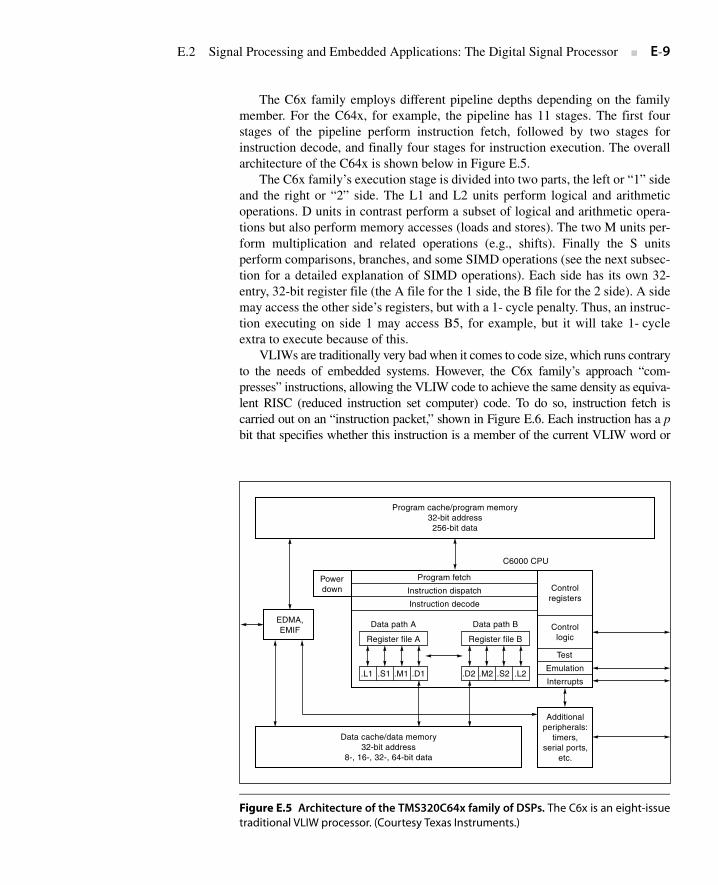
The C6x family employs different pipeline depths depending on the familymember. For the C64x, for example, the pipeline has 11 stages. The first fourstages of the pipeline perform instruction fetch, followed by two stages forinstruction decode, and finally four stages for instruction execution. The overallarchitecture of the C64x is shown below in Figure E.5.
The C6x family’s execution stage is divided into two parts, the left or “1” sideand the right or “2” side. The L1 and L2 units perform logical and arithmeticoperations. D units in contrast perform a subset of logical and arithmetic opera-tions but also perform memory accesses (loads and stores). The two M units per-form multiplication and related operations (e.g., shifts). Finally the S unitsperform comparisons, branches, and some SIMD operations (see the next subsec-tion for a detailed explanation of SIMD operations). Each side has its own 32-entry, 32-bit register file (the A file for the 1 side, the B file for the 2 side). A sidemay access the other side’s registers, but with a 1- cycle penalty. Thus, an instruc-tion executing on side 1 may access B5, for example, but it will take 1- cycleextra to execute because of this.
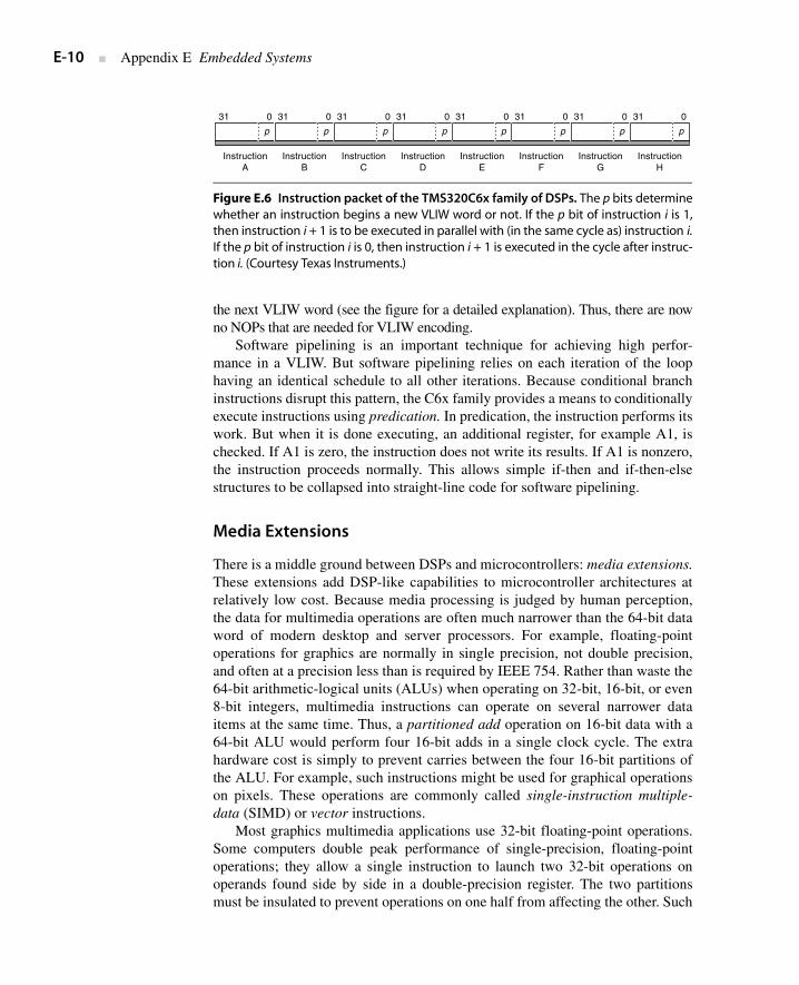
VLIWs are traditionally very bad when it comes to code size, which runs contraryto the needs of embedded systems. However, the C6x family’s approach “com-presses” instructions, allowing the VLIW code to achieve the same density as equiva-lent RISC (reduced instruction set computer) code. To do so, instruction fetch iscarried out on an “instruction packet,” shown in Figure E.6. Each instruction has a pbit that specifies whether this instruction is a member of the current VLIW word or
Figure E.5 Architecture of the TMS320C64x family of DSPs. The C6x is an eight-issuetraditional VLIW processor. (Courtesy Texas Instruments.)
Program cache/program memory32-bit address256-bit data
Data cache/data memory32-bit address
8-, 16-, 32-, 64-bit data
Program fetch
Instruction dispatch
Instruction decode
Controlregisters
C6000 CPU
Controllogic
Test
Emulation
Interrupts
EDMA,EMIF
Additionalperipherals:
timers,serial ports,
etc.
Register file A
Data path A
.L1 .S1 .M1 .D1
Powerdown
Register file B
Data path B
.D2 .M2 .S2 .L2
E-10 ■ Appendix E Embedded Systems
the next VLIW word (see the figure for a detailed explanation). Thus, there are nowno NOPs that are needed for VLIW encoding.
Software pipelining is an important technique for achieving high perfor-mance in a VLIW. But software pipelining relies on each iteration of the loophaving an identical schedule to all other iterations. Because conditional branchinstructions disrupt this pattern, the C6x family provides a means to conditionallyexecute instructions using predication. In predication, the instruction performs itswork. But when it is done executing, an additional register, for example A1, ischecked. If A1 is zero, the instruction does not write its results. If A1 is nonzero,the instruction proceeds normally. This allows simple if-then and if-then-elsestructures to be collapsed into straight-line code for software pipelining.
Media Extensions
There is a middle ground between DSPs and microcontrollers: media extensions.These extensions add DSP-like capabilities to microcontroller architectures atrelatively low cost. Because media processing is judged by human perception,the data for multimedia operations are often much narrower than the 64-bit dataword of modern desktop and server processors. For example, floating-pointoperations for graphics are normally in single precision, not double precision,and often at a precision less than is required by IEEE 754. Rather than waste the64-bit arithmetic-logical units (ALUs) when operating on 32-bit, 16-bit, or even8-bit integers, multimedia instructions can operate on several narrower dataitems at the same time. Thus, a partitioned add operation on 16-bit data with a64-bit ALU would perform four 16-bit adds in a single clock cycle. The extrahardware cost is simply to prevent carries between the four 16-bit partitions ofthe ALU. For example, such instructions might be used for graphical operationson pixels. These operations are commonly called single-instruction multiple-data (SIMD) or vector instructions.
Most graphics multimedia applications use 32-bit floating-point operations.Some computers double peak performance of single-precision, floating-pointoperations; they allow a single instruction to launch two 32-bit operations onoperands found side by side in a double-precision register. The two partitionsmust be insulated to prevent operations on one half from affecting the other. Such
Figure E.6 Instruction packet of the TMS320C6x family of DSPs. The p bits determinewhether an instruction begins a new VLIW word or not. If the p bit of instruction i is 1,then instruction i + 1 is to be executed in parallel with (in the same cycle as) instruction i.If the p bit of instruction i is 0, then instruction i + 1 is executed in the cycle after instruc-tion i. (Courtesy Texas Instruments.)
31 0 31 0 31 0 31 0 31 0 31 0 31 0 31 0
InstructionA
p p p p p p p p
InstructionB
InstructionC
InstructionD
InstructionE
InstructionF
InstructionG
InstructionH
E.2 Signal Processing and Embedded Applications: The Digital Signal Processor ■ E-11
floating-point operations are called paired single operations. For example, suchan operation might be used for graphical transformations of vertices. Thisdoubling in performance is typically accomplished by doubling the number offloating-point units, making it more expensive than just suppressing carries ininteger adders.
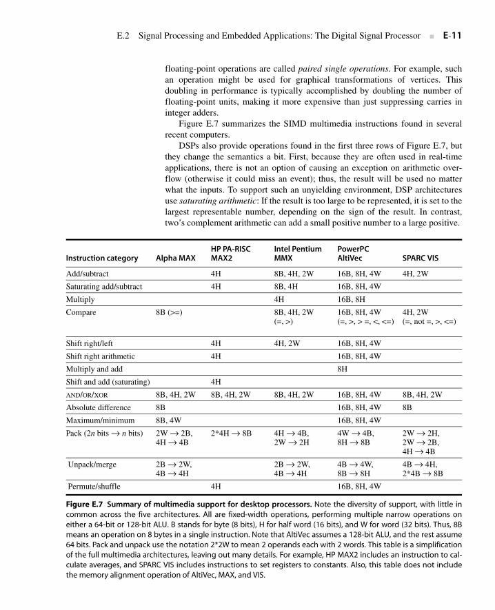
Figure E.7 summarizes the SIMD multimedia instructions found in severalrecent computers.
DSPs also provide operations found in the first three rows of Figure E.7, butthey change the semantics a bit. First, because they are often used in real-timeapplications, there is not an option of causing an exception on arithmetic over-flow (otherwise it could miss an event); thus, the result will be used no matterwhat the inputs. To support such an unyielding environment, DSP architecturesuse saturating arithmetic: If the result is too large to be represented, it is set to thelargest representable number, depending on the sign of the result. In contrast,two’s complement arithmetic can add a small positive number to a large positive.
Instruction category Alpha MAXHP PA-RISC MAX2
Intel Pentium MMX
PowerPC AltiVec SPARC VIS
Add/subtract 4H 8B, 4H, 2W 16B, 8H, 4W 4H, 2W
Saturating add/subtract 4H 8B, 4H 16B, 8H, 4W
Multiply 4H 16B, 8H
Compare 8B (>=) 8B, 4H, 2W (=, >)
16B, 8H, 4W (=, >, > =, <, <=)
4H, 2W(=, not =, >, <=)
Shift right/left 4H 4H, 2W 16B, 8H, 4W
Shift right arithmetic 4H 16B, 8H, 4W
Multiply and add 8H
Shift and add (saturating) 4H
AND/OR/XOR 8B, 4H, 2W 8B, 4H, 2W 8B, 4H, 2W 16B, 8H, 4W 8B, 4H, 2W
Absolute difference 8B 16B, 8H, 4W 8B
Maximum/minimum 8B, 4W 16B, 8H, 4W
Pack (2n bits → n bits) 2W → 2B,4H → 4B
2*4H → 8B 4H → 4B, 2W → 2H
4W → 4B, 8H → 8B
2W → 2H, 2W → 2B, 4H → 4B
Unpack/merge 2B → 2W, 4B → 4H
2B → 2W, 4B → 4H
4B → 4W, 8B → 8H
4B → 4H, 2*4B → 8B
Permute/shuffle 4H 16B, 8H, 4W
Figure E.7 Summary of multimedia support for desktop processors. Note the diversity of support, with little incommon across the five architectures. All are fixed-width operations, performing multiple narrow operations oneither a 64-bit or 128-bit ALU. B stands for byte (8 bits), H for half word (16 bits), and W for word (32 bits). Thus, 8Bmeans an operation on 8 bytes in a single instruction. Note that AltiVec assumes a 128-bit ALU, and the rest assume64 bits. Pack and unpack use the notation 2*2W to mean 2 operands each with 2 words. This table is a simplificationof the full multimedia architectures, leaving out many details. For example, HP MAX2 includes an instruction to cal-culate averages, and SPARC VIS includes instructions to set registers to constants. Also, this table does not includethe memory alignment operation of AltiVec, MAX, and VIS.
E-12 ■ Appendix E Embedded Systems
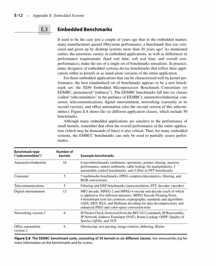
It used to be the case just a couple of years ago that in the embedded market,many manufacturers quoted Dhrystone performance, a benchmark that was criti-cized and given up by desktop systems more than 20 years ago! As mentionedearlier, the enormous variety in embedded applications, as well as differences inperformance requirements (hard real time, soft real time, and overall cost-performance), make the use of a single set of benchmarks unrealistic. In practice,many designers of embedded systems devise benchmarks that reflect their appli-cation, either as kernels or as stand-alone versions of the entire application.
For those embedded applications that can be characterized well by kernel per-formance, the best standardized set of benchmarks appears to be a new bench-mark set: the EDN Embedded Microprocessor Benchmark Consortium (orEEMBC, pronounced “embassy”). The EEMBC benchmarks fall into six classes(called “subcommittees” in the parlance of EEMBC): automotive/industrial, con-sumer, telecommunications, digital entertainment, networking (currently in itssecond version), and office automation (also the second version of this subcom-mittee). Figure E.8 shows the six different application classes, which include 50benchmarks.
Although many embedded applications are sensitive to the performance ofsmall kernels, remember that often the overall performance of the entire applica-tion (which may be thousands of lines) is also critical. Thus, for many embeddedsystems, the EMBCC benchmarks can only be used to partially assess perfor-mance.
Benchmark type (“subcommittee”)
Number of kernels Example benchmarks
Automotive/industrial 16 6 microbenchmarks (arithmetic operations, pointer chasing, memory performance, matrix arithmetic, table lookup, bit manipulation), 5 automobile control benchmarks, and 5 filter or FFT benchmarks
Consumer 5 5 multimedia benchmarks (JPEG compress/decompress, filtering, and RGB conversions)
Telecommunications 5 Filtering and DSP benchmarks (autocorrelation, FFT, decoder, encoder)
Digital entertainment 12 MP3 decode, MPEG-2 and MPEG-4 encode and decode (each of which is applied to five different datasets), MPEG Encode Floating Point, 4 benchmark tests for common cryptographic standards and algorithms (AES, DES, RSA, and Huffman decoding for data decompression), and enhanced JPEG and color-space conversion tests
Networking version 2 6 IP Packet Check (borrowed from the RFC1812 standard), IP Reassembly, IP Network Address Translator (NAT), Route Lookup, OSPF, Quality of Service (QOS), and TCP
Office automation version 2
6 Ghostscript, text parsing, image rotation, dithering, Bézier
Figure E.8 The EEMBC benchmark suite, consisting of 50 kernels in six different classes. See www.eembc.org formore information on the benchmarks and for scores.
E.3 Embedded Benchmarks
E.3 Embedded Benchmarks ■ E-13
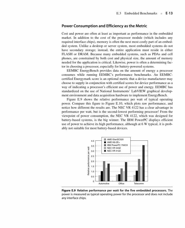
Power Consumption and Efficiency as the Metric
Cost and power are often at least as important as performance in the embeddedmarket. In addition to the cost of the processor module (which includes anyrequired interface chips), memory is often the next most costly part of an embed-ded system. Unlike a desktop or server system, most embedded systems do nothave secondary storage; instead, the entire application must reside in eitherFLASH or DRAM. Because many embedded systems, such as PDAs and cellphones, are constrained by both cost and physical size, the amount of memoryneeded for the application is critical. Likewise, power is often a determining fac-tor in choosing a processor, especially for battery-powered systems.
EEMBC EnergyBench provides data on the amount of energy a processorconsumes while running EEMBC’s performance benchmarks. An EEMBC-certified Energymark score is an optional metric that a device manufacturer maychoose to supply in conjunction with certified scores for device performance as away of indicating a processor’s efficient use of power and energy. EEMBC hasstandardized on the use of National Instruments’ LabVIEW graphical develop-ment environment and data acquisition hardware to implement EnergyBench.
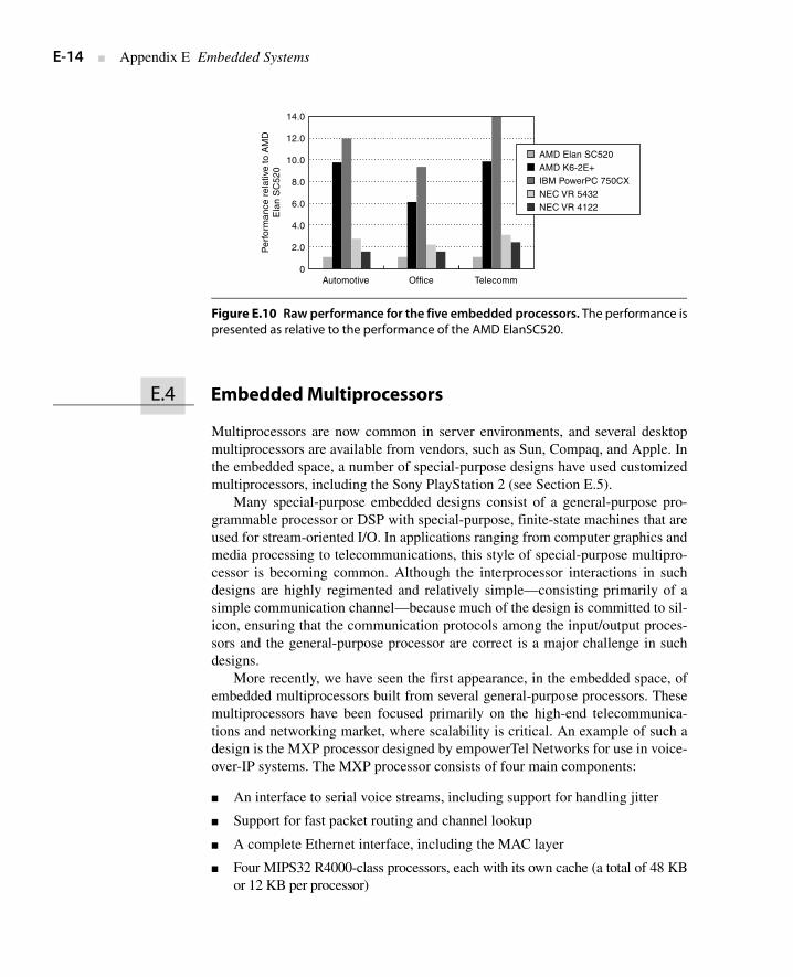
Figure E.9 shows the relative performance per watt of typical operatingpower. Compare this figure to Figure E.10, which plots raw performance, andnotice how different the results are. The NEC VR 4122 has a clear advantage inperformance per watt, but is the second-lowest performing processor! From theviewpoint of power consumption, the NEC VR 4122, which was designed forbattery-based systems, is the big winner. The IBM PowerPC displays efficientuse of power to achieve its high performance, although at 6 W typical, it is prob-ably not suitable for most battery-based devices.
Figure E.9 Relative performance per watt for the five embedded processors. Thepower is measured as typical operating power for the processor and does not includeany interface chips.
Rel
ativ
e pe
rfor
man
ce p
er w
att
0
3.5
4.0
3.0
2.5
2.0
1.5
1.0
0.5
Automotive Office Telecomm
AMD ElanSC520AMD K6-2E+IBM PowerPC 750CXNEC VR 5432NEC VR 4122
E-14 ■ Appendix E Embedded Systems
Multiprocessors are now common in server environments, and several desktopmultiprocessors are available from vendors, such as Sun, Compaq, and Apple. Inthe embedded space, a number of special-purpose designs have used customizedmultiprocessors, including the Sony PlayStation 2 (see Section E.5).
Many special-purpose embedded designs consist of a general-purpose pro-grammable processor or DSP with special-purpose, finite-state machines that areused for stream-oriented I/O. In applications ranging from computer graphics andmedia processing to telecommunications, this style of special-purpose multipro-cessor is becoming common. Although the interprocessor interactions in suchdesigns are highly regimented and relatively simple—consisting primarily of asimple communication channel—because much of the design is committed to sil-icon, ensuring that the communication protocols among the input/output proces-sors and the general-purpose processor are correct is a major challenge in suchdesigns.
More recently, we have seen the first appearance, in the embedded space, ofembedded multiprocessors built from several general-purpose processors. Thesemultiprocessors have been focused primarily on the high-end telecommunica-tions and networking market, where scalability is critical. An example of such adesign is the MXP processor designed by empowerTel Networks for use in voice-over-IP systems. The MXP processor consists of four main components:
■ An interface to serial voice streams, including support for handling jitter
■ Support for fast packet routing and channel lookup
■ A complete Ethernet interface, including the MAC layer
■ Four MIPS32 R4000-class processors, each with its own cache (a total of 48 KBor 12 KB per processor)
Figure E.10 Raw performance for the five embedded processors. The performance ispresented as relative to the performance of the AMD ElanSC520.
Per
form
ance
rel
ativ
e to
AM
DE
lan
SC
520
14.0
12.0
10.0
8.0
6.0
4.0
2.0
0Automotive Office Telecomm
AMD Elan SC520AMD K6-2E+IBM PowerPC 750CXNEC VR 5432NEC VR 4122
E.4 Embedded Multiprocessors
E.5 Case Study: The Emotion Engine of the Sony PlayStation 2 ■ E-15
The MIPS processors are used to run the code responsible for maintainingthe voice-over-IP channels, including the assurance of quality of service, echocancellation, simple compression, and packet encoding. Since the goal is to runas many independent voice streams as possible, a multiprocessor is an idealsolution.
Because of the small size of the MIPS cores, the entire chip takes only 13.5Mtransistors. Future generations of the chip are expected to handle more voicechannels, as well as do more sophisticated echo cancellation, voice activitydetection, and more sophisticated compression.
Multiprocessing is becoming widespread in the embedded computing arenafor two primary reasons. First, the issues of binary software compatibility, whichplague desktop and server systems, are less relevant in the embedded space.Often software in an embedded application is written from scratch for an applica-tion or significantly modified (note that this is also the reason VLIW is favoredover superscalar in embedded instruction-level parallelism). Second, the applica-tions often have natural parallelism, especially at the high end of the embeddedspace. Examples of this natural parallelism abound in applications such as a set-top box, a network switch, a cell phone (see Section E.7) or a game system (seeSection E.5). The lower barriers to use of thread-level parallelism together withthe greater sensitivity to die cost (and hence efficient use of silicon) are leading towidespread adoption of multiprocessing in the embedded space, as the applica-tion needs grow to demand more performance.
Desktop computers and servers rely on the memory hierarchy to reduce averageaccess time to relatively static data, but there are embedded applications wheredata are often a continuous stream. In such applications there is still spatial local-ity, but temporal locality is much more limited.
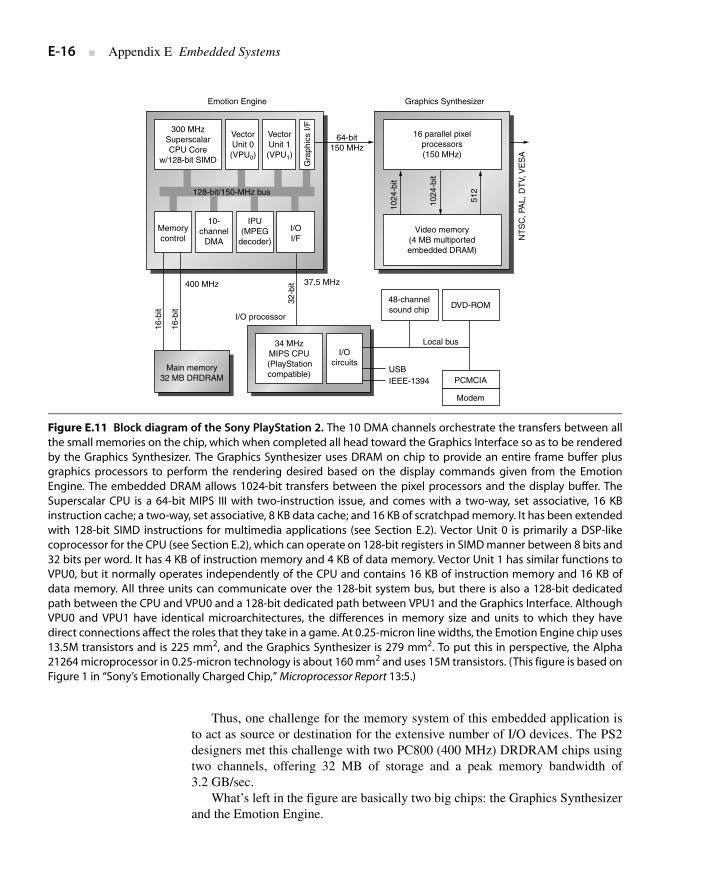
To give another look at memory performance beyond the desktop, this sectionexamines the microprocessor at the heart of the Sony PlayStation 2. As we willsee, the steady stream of graphics and audio demanded by electronic games leadsto a different approach to memory design. The style is high bandwidth via manydedicated independent memories.
Figure E.11 shows a block diagram of the Sony PlayStation 2 (PS2). Not sur-prisingly for a game machine, there are interfaces for video, sound, and a DVDplayer. Surprisingly, there are two standard computer I/O buses, USB and IEEE1394, a PCMCIA slot as found in portable PCs, and a modem. These additionsshow that Sony had greater plans for the PS2 beyond traditional games. Althoughit appears that the I/O processor (IOP) simply handles the I/O devices and thegame console, it includes a 34 MHz MIPS processor that also acts as the emula-tion computer to run games for earlier Sony PlayStations. It also connects to astandard PC audio card to provide the sound for the games.
E.5 Case Study: The Emotion Engine of the Sony PlayStation 2
E-16 ■ Appendix E Embedded Systems
Thus, one challenge for the memory system of this embedded application isto act as source or destination for the extensive number of I/O devices. The PS2designers met this challenge with two PC800 (400 MHz) DRDRAM chips usingtwo channels, offering 32 MB of storage and a peak memory bandwidth of3.2 GB/sec.
What’s left in the figure are basically two big chips: the Graphics Synthesizerand the Emotion Engine.
Figure E.11 Block diagram of the Sony PlayStation 2. The 10 DMA channels orchestrate the transfers between allthe small memories on the chip, which when completed all head toward the Graphics Interface so as to be renderedby the Graphics Synthesizer. The Graphics Synthesizer uses DRAM on chip to provide an entire frame buffer plusgraphics processors to perform the rendering desired based on the display commands given from the EmotionEngine. The embedded DRAM allows 1024-bit transfers between the pixel processors and the display buffer. TheSuperscalar CPU is a 64-bit MIPS III with two-instruction issue, and comes with a two-way, set associative, 16 KBinstruction cache; a two-way, set associative, 8 KB data cache; and 16 KB of scratchpad memory. It has been extendedwith 128-bit SIMD instructions for multimedia applications (see Section E.2). Vector Unit 0 is primarily a DSP-likecoprocessor for the CPU (see Section E.2), which can operate on 128-bit registers in SIMD manner between 8 bits and32 bits per word. It has 4 KB of instruction memory and 4 KB of data memory. Vector Unit 1 has similar functions toVPU0, but it normally operates independently of the CPU and contains 16 KB of instruction memory and 16 KB ofdata memory. All three units can communicate over the 128-bit system bus, but there is also a 128-bit dedicatedpath between the CPU and VPU0 and a 128-bit dedicated path between VPU1 and the Graphics Interface. AlthoughVPU0 and VPU1 have identical microarchitectures, the differences in memory size and units to which they havedirect connections affect the roles that they take in a game. At 0.25-micron line widths, the Emotion Engine chip uses13.5M transistors and is 225 mm2, and the Graphics Synthesizer is 279 mm2. To put this in perspective, the Alpha21264 microprocessor in 0.25-micron technology is about 160 mm2 and uses 15M transistors. (This figure is based onFigure 1 in “Sony’s Emotionally Charged Chip,” Microprocessor Report 13:5.)
300 MHzSuperscalarCPU Core
w/128-bit SIMD
Emotion Engine
I/O processor
Graphics Synthesizer
16 parallel pixelprocessors(150 MHz)
Video memory(4 MB multiportedembedded DRAM)
Memorycontrol
10-channel
DMA
IPU(MPEG
decoder)
I/OI/F
VectorUnit 0(VPU0)
128-bit/150-MHz bus
VectorUnit 1(VPU1)
64-bit
16-b
it
16-b
it
150 MHz
400 MHz
Gra
phic
s I/F
32-b
it
1024
-bit
NT
SC
, PA
L, D
TV,
VE
SA
1024
-bit
512
37.5 MHz
Main memory32 MB DRDRAM
34 MHzMIPS CPU(PlayStationcompatible)
48-channelsound chip
Local bus
USB
DVD-ROM
PCMCIA
Modem
I/Ocircuits
IEEE-1394
E.5 Case Study: The Emotion Engine of the Sony PlayStation 2 ■ E-17
The Graphics Synthesizer takes rendering commands from the EmotionEngine in what are commonly called display lists. These are lists of 32-bit com-mands that tell the renderer what shape to use and where to place them, plus whatcolors and textures to fill them.
This chip also has the highest bandwidth portion of the memory system. Byusing embedded DRAM on the Graphics Synthesizer, the chip contains the fullvideo buffer and has a 2048-bit-wide interface so that pixel filling is not a bottle-neck. This embedded DRAM greatly reduces the bandwidth demands on theDRDRAM. It illustrates a common technique found in embedded applications:separate memories dedicated to individual functions to inexpensively achievegreater memory bandwidth for the entire system.
The remaining large chip is the Emotion Engine, and its job is to acceptinputs from the IOP and create the display lists of a video game to enable 3Dvideo transformations in real time. A major insight shaped the design of the Emo-tion Engine: Generally, in a racing car game there are foreground objects that areconstantly changing and background objects that change less in reaction to theevents, although the background can be most of the screen. This observation ledto a split of responsibilities.
The CPU works with VPU0 as a tightly coupled coprocessor, in that everyVPU0 instruction is a standard MIPS coprocessor instruction, and the addressesare generated by the MIPS CPU. VPU0 is called a vector processor, but it is sim-ilar to 128-bit SIMD extensions for multimedia found in several desktop proces-sors (see Section E.2).
VPU1, in contrast, fetches its own instructions and data and acts in parallelwith CPU/VPU0, acting more like a traditional vector unit. With this split, themore flexible CPU/VPU0 handles the foreground action and the VPU1 handlesthe background. Both deposit their resulting display lists into the Graphics Inter-face to send the lists to the Graphics Synthesizer.
Thus, the programmers of the Emotion Engine have three processor sets tochoose from to implement their programs: the traditional 64-bit MIPS architec-ture including a floating-point unit, the MIPS architecture extended with multi-media instructions (VPU0), and an independent vector processor (VPU1). Toaccelerate MPEG decoding, there is another coprocessor (Image ProcessingUnit) that can act independent of the other two.
With this split of function, the question then is how to connect the unitstogether, how to make the data flow between units, and how to provide the mem-ory bandwidth needed by all these units. As mentioned earlier, the EmotionEngine designers chose many dedicated memories. The CPU has a 16 KB scratchpad memory (SPRAM) in addition to a 16 KB instruction cache and an 8 KB datacache. VPU0 has a 4 KB instruction memory and a 4 KB data memory, andVPU1 has a 16 KB instruction memory and a 16 KB data memory. Note thatthese are four memories, not caches of a larger memory elsewhere. In each mem-ory the latency is just 1 clock cycle. VPU1 has more memory than VPU0 becauseit creates the bulk of the display lists and because it largely acts independently.
E-18 ■ Appendix E Embedded Systems
The programmer organizes all memories as two double buffers, one pair forthe incoming DMA data and one pair for the outgoing DMA data. The program-mer then uses the various processors to transform the data from the input bufferto the output buffer. To keep the data flowing among the units, the programmernext sets up the 10 DMA channels, taking care to meet the real-time deadline forrealistic animation of 15 frames per second.
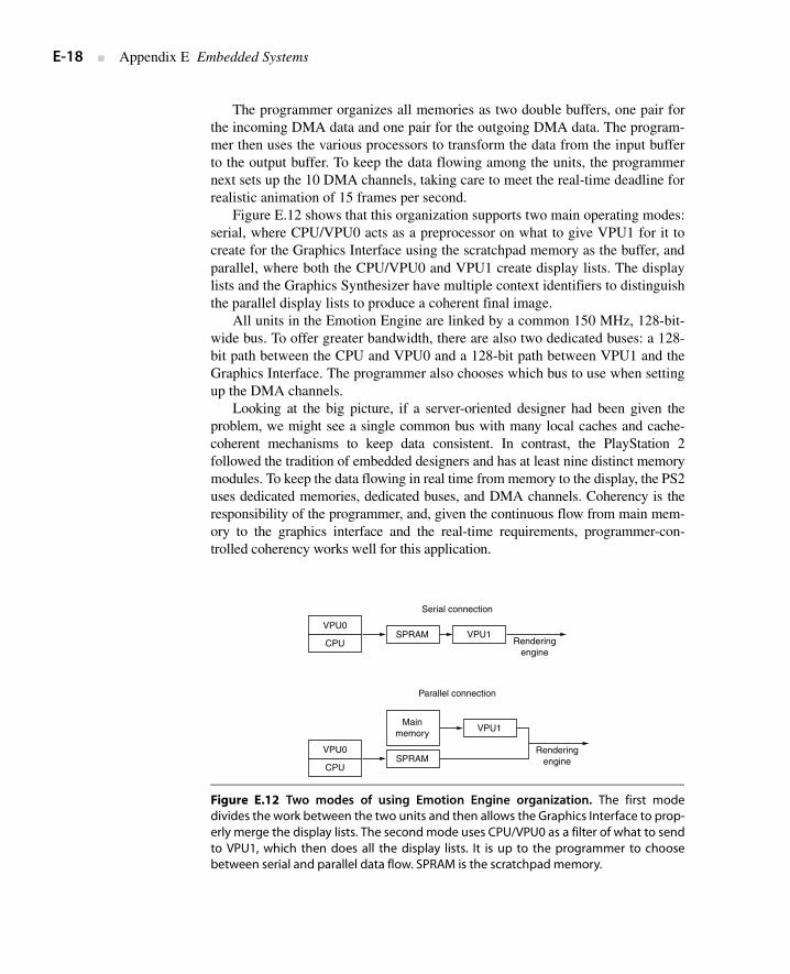
Figure E.12 shows that this organization supports two main operating modes:serial, where CPU/VPU0 acts as a preprocessor on what to give VPU1 for it tocreate for the Graphics Interface using the scratchpad memory as the buffer, andparallel, where both the CPU/VPU0 and VPU1 create display lists. The displaylists and the Graphics Synthesizer have multiple context identifiers to distinguishthe parallel display lists to produce a coherent final image.
All units in the Emotion Engine are linked by a common 150 MHz, 128-bit-wide bus. To offer greater bandwidth, there are also two dedicated buses: a 128-bit path between the CPU and VPU0 and a 128-bit path between VPU1 and theGraphics Interface. The programmer also chooses which bus to use when settingup the DMA channels.
Looking at the big picture, if a server-oriented designer had been given theproblem, we might see a single common bus with many local caches and cache-coherent mechanisms to keep data consistent. In contrast, the PlayStation 2followed the tradition of embedded designers and has at least nine distinct memorymodules. To keep the data flowing in real time from memory to the display, the PS2uses dedicated memories, dedicated buses, and DMA channels. Coherency is theresponsibility of the programmer, and, given the continuous flow from main mem-ory to the graphics interface and the real-time requirements, programmer-con-trolled coherency works well for this application.
Figure E.12 Two modes of using Emotion Engine organization. The first modedivides the work between the two units and then allows the Graphics Interface to prop-erly merge the display lists. The second mode uses CPU/VPU0 as a filter of what to sendto VPU1, which then does all the display lists. It is up to the programmer to choosebetween serial and parallel data flow. SPRAM is the scratchpad memory.
VPU0SPRAM
Parallel connection
VPU1
Renderingengine
Mainmemory
CPU
VPU0SPRAM
Serial connection
Renderingengine
CPUVPU1
E.6 Case Study: Sanyo VPC-SX500 Digital Camera ■ E-19
Another very familiar embedded system is a digital camera. Here we consider theSanyo VPC-SX500. When powered on, the microprocessor of the camera firstruns diagnostics on all components and writes any error messages to the liquidcrystal display (LCD) on the back of the camera. This camera uses a 1.8-inchlow-temperature polysilicon thin-film transistor (TFT) color LCD. When a pho-tographer takes a picture, he first holds the shutter halfway so that the micropro-cessor can take a light reading. The microprocessor then keeps the shutter open toget the necessary light, which is captured by a charge-coupled device (CCD) asred, green, and blue pixels. The CCD is a 1/2-inch, 1360 × 1024-pixel, progres-sive-scan chip. The pixels are scanned out row by row; passed through routinesfor white balance, color, and aliasing correction; and then stored in a 4 MB framebuffer. The next step is to compress the image into a standard format, such asJPEG, and store it in the removable Flash memory. The photographer picks thecompression, in this camera called either fine or normal, with a compression ratioof 10 to 20 times. A 512 MB Flash memory can store at least 1200 fine-qualitycompressed images or approximately 2000 normal-quality compressed images.The microprocessor then updates the LCD display to show that there is room forone less picture.
Although the previous paragraph covers the basics of a digital camera, thereare many more features that are included: showing the recorded images on thecolor LCD display, sleep mode to save battery life, monitoring battery energy,buffering to allow recording a rapid sequence of uncompressed images, and, inthis camera, video recording using MPEG format and audio recording usingWAV format.
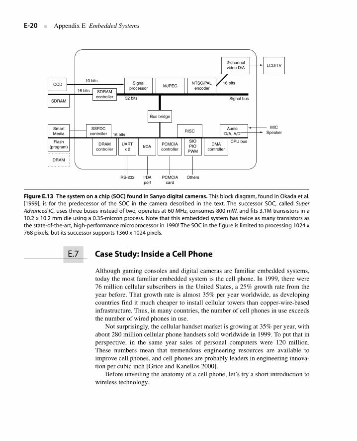
The electronic brain of this camera is an embedded computer with severalspecial functions embedded on the chip [Okada et al. 1999]. Figure E.13 showsthe block diagram of a chip similar to the one in the camera. As mentioned inSection E.1, such chips have been called systems on a chip (SOCs) because theyessentially integrate into a single chip all the parts that were found on a smallprinted circuit board of the past. A SOC generally reduces size and lowers powercompared to less integrated solutions. Sanyo claims their SOC enables the cam-era to operate on half the number of batteries and to offer a smaller form factorthan competitors’ cameras. For higher performance, it has two buses. The 16-bitbus is for the many slower I/O devices: SmartMedia interface, program and datamemory, and DMA. The 32-bit bus is for the SDRAM, the signal processor(which is connected to the CCD), the Motion JPEG encoder, and the NTSC/PALencoder (which is connected to the LCD). Unlike desktop microprocessors, notethe large variety of I/O buses that this chip must integrate. The 32-bit RISC MPUis a proprietary design and runs at 28.8 MHz, the same clock rate as the buses.This 700 mW chip contains 1.8M transistors in a 10.5 × 10.5 mm die imple-mented using a 0.35-micron process.
E.6 Case Study: Sanyo VPC-SX500 Digital Camera
E-20 ■ Appendix E Embedded Systems
Although gaming consoles and digital cameras are familiar embedded systems,today the most familiar embedded system is the cell phone. In 1999, there were76 million cellular subscribers in the United States, a 25% growth rate from theyear before. That growth rate is almost 35% per year worldwide, as developingcountries find it much cheaper to install cellular towers than copper-wire-basedinfrastructure. Thus, in many countries, the number of cell phones in use exceedsthe number of wired phones in use.
Not surprisingly, the cellular handset market is growing at 35% per year, withabout 280 million cellular phone handsets sold worldwide in 1999. To put that inperspective, in the same year sales of personal computers were 120 million.These numbers mean that tremendous engineering resources are available toimprove cell phones, and cell phones are probably leaders in engineering innova-tion per cubic inch [Grice and Kanellos 2000].
Before unveiling the anatomy of a cell phone, let’s try a short introduction towireless technology.
Figure E.13 The system on a chip (SOC) found in Sanyo digital cameras. This block diagram, found in Okada et al.[1999], is for the predecessor of the SOC in the camera described in the text. The successor SOC, called SuperAdvanced IC, uses three buses instead of two, operates at 60 MHz, consumes 800 mW, and fits 3.1M transistors in a10.2 x 10.2 mm die using a 0.35-micron process. Note that this embedded system has twice as many transistors asthe state-of-the-art, high-performance microprocessor in 1990! The SOC in the figure is limited to processing 1024 x768 pixels, but its successor supports 1360 x 1024 pixels.
AudioD/A, A/D
DRAMcontroller
DMAcontroller
PCMCIAcontroller
UARTx 2
SIOPIO
PWMIrDA
CCD
SDRAM
DRAM
Signalprocessor MJPEG
NTSC/PALencoder
2-channelvideo D/A LCD/TV
MICSpeaker
SmartMedia
Flash(program)
SSFDCcontroller
RISC
SDRAMcontroller
RS-232
16 bits
16 bits
32 bits
10 bits
16 bits
Signal bus
CPU bus
Bus bridge
IrDAport
PCMCIAcard
Others
E.7 Case Study: Inside a Cell Phone
E.7 Case Study: Inside a Cell Phone ■ E-21
Background on Wireless Networks
Networks can be created out of thin air as well as out of copper and glass, creat-ing wireless networks. Much of this section is based on a report from the NationalResearch Council [1997].
A radio wave is an electromagnetic wave propagated by an antenna. Radiowaves are modulated, which means that the sound signal is superimposed on thestronger radio wave that carries the sound signal, and hence is called the carriersignal. Radio waves have a particular wavelength or frequency: They are mea-sured either as the length of the complete wave or as the number of waves persecond. Long waves have low frequencies, and short waves have high frequen-cies. FM radio stations transmit on the band of 88 MHz to 108 MHz using fre-quency modulations (FM) to record the sound signal.
By tuning in to different frequencies, a radio receiver can pick up a specificsignal. In addition to AM and FM radio, other frequencies are reserved for citi-zens band radio, television, pagers, air traffic control radar, Global PositioningSystem, and so on. In the United States, the Federal Communications Commis-sion decides who gets to use which frequencies and for what purpose.
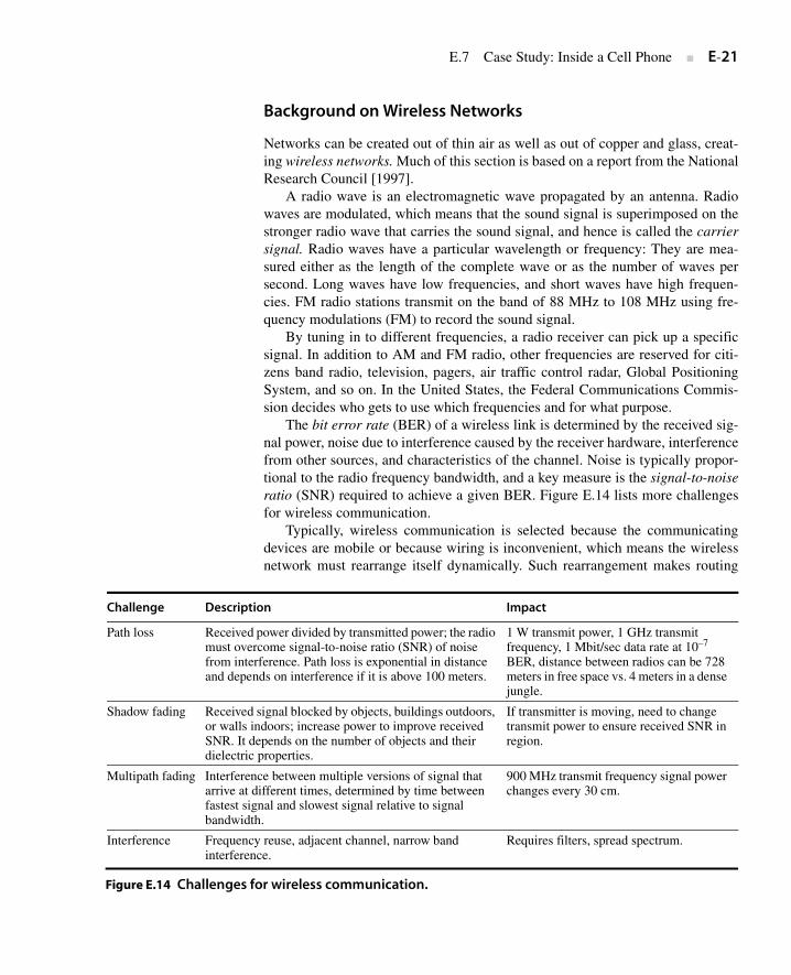
The bit error rate (BER) of a wireless link is determined by the received sig-nal power, noise due to interference caused by the receiver hardware, interferencefrom other sources, and characteristics of the channel. Noise is typically propor-tional to the radio frequency bandwidth, and a key measure is the signal-to-noiseratio (SNR) required to achieve a given BER. Figure E.14 lists more challengesfor wireless communication.
Typically, wireless communication is selected because the communicatingdevices are mobile or because wiring is inconvenient, which means the wirelessnetwork must rearrange itself dynamically. Such rearrangement makes routing
Challenge Description Impact
Path loss Received power divided by transmitted power; the radio must overcome signal-to-noise ratio (SNR) of noise from interference. Path loss is exponential in distance and depends on interference if it is above 100 meters.
1 W transmit power, 1 GHz transmit frequency, 1 Mbit/sec data rate at 10–7
BER, distance between radios can be 728 meters in free space vs. 4 meters in a dense jungle.
Shadow fading Received signal blocked by objects, buildings outdoors, or walls indoors; increase power to improve received SNR. It depends on the number of objects and their dielectric properties.
If transmitter is moving, need to change transmit power to ensure received SNR in region.
Multipath fading Interference between multiple versions of signal that arrive at different times, determined by time between fastest signal and slowest signal relative to signal bandwidth.
900 MHz transmit frequency signal power changes every 30 cm.
Interference Frequency reuse, adjacent channel, narrow band interference.
Requires filters, spread spectrum.
Figure E.14 Challenges for wireless communication.
E-22 ■ Appendix E Embedded Systems
more challenging. A second challenge is that wireless signals are not protectedand hence are subject to mutual interference, especially as devices move. Poweris another challenge for wireless communication, both because the devices tendto be battery powered and because antennas radiate power to communicate andlittle of it reaches the receiver. As a result, raw bit error rates are typically a thou-sand to a million times higher than copper wire.
There are two primary architectures for wireless networks: base station archi-tectures and peer-to-peer architectures. Base stations are connected by landlinesfor longer-distance communication, and the mobile units communicate only witha single local base station. Peer-to-peer architectures allow mobile units to com-municate with each other, and messages hop from one unit to the next until deliv-ered to the desired unit. Although peer-to-peer is more reconfigurable, basestations tend to be more reliable since there is only one hop between the deviceand the station. Cellular telephony, the most popular example of wireless net-works, relies on radio with base stations.
Cellular systems exploit exponential path loss to reuse the same frequency atspatially separated locations, thereby greatly increasing the number of customersserved. Cellular systems will divide a city into nonoverlapping hexagonal cellsthat use different frequencies if nearby, reusing a frequency only when cells arefar enough apart so that mutual interference is acceptable.
At the intersection of three hexagonal cells is a base station with transmittersand antennas that is connected to a switching office that coordinates handoffswhen a mobile device leaves one cell and goes into another, as well as acceptsand places calls over landlines. Depending on topography, population, and so on,the radius of a typical cell is 2 to 10 miles.
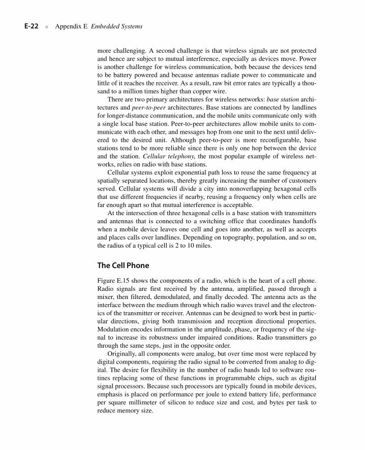
The Cell Phone
Figure E.15 shows the components of a radio, which is the heart of a cell phone.Radio signals are first received by the antenna, amplified, passed through amixer, then filtered, demodulated, and finally decoded. The antenna acts as theinterface between the medium through which radio waves travel and the electron-ics of the transmitter or receiver. Antennas can be designed to work best in partic-ular directions, giving both transmission and reception directional properties.Modulation encodes information in the amplitude, phase, or frequency of the sig-nal to increase its robustness under impaired conditions. Radio transmitters gothrough the same steps, just in the opposite order.
Originally, all components were analog, but over time most were replaced bydigital components, requiring the radio signal to be converted from analog to dig-ital. The desire for flexibility in the number of radio bands led to software rou-tines replacing some of these functions in programmable chips, such as digitalsignal processors. Because such processors are typically found in mobile devices,emphasis is placed on performance per joule to extend battery life, performanceper square millimeter of silicon to reduce size and cost, and bytes per task toreduce memory size.
E.7 Case Study: Inside a Cell Phone ■ E-23
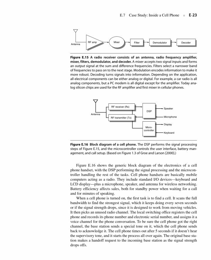
Figure E.16 shows the generic block diagram of the electronics of a cellphone handset, with the DSP performing the signal processing and the microcon-troller handling the rest of the tasks. Cell phone handsets are basically mobilecomputers acting as a radio. They include standard I/O devices—keyboard andLCD display—plus a microphone, speaker, and antenna for wireless networking.Battery efficiency affects sales, both for standby power when waiting for a calland for minutes of speaking.
When a cell phone is turned on, the first task is to find a cell. It scans the fullbandwidth to find the strongest signal, which it keeps doing every seven secondsor if the signal strength drops, since it is designed to work from moving vehicles.It then picks an unused radio channel. The local switching office registers the cellphone and records its phone number and electronic serial number, and assigns it avoice channel for the phone conversation. To be sure the cell phone got the rightchannel, the base station sends a special tone on it, which the cell phone sendsback to acknowledge it. The cell phone times out after 5 seconds if it doesn’t hearthe supervisory tone, and it starts the process all over again. The original base sta-tion makes a handoff request to the incoming base station as the signal strengthdrops offs.
Figure E.15 A radio receiver consists of an antenna, radio frequency amplifier,mixer, filters, demodulator, and decoder. A mixer accepts two signal inputs and formsan output signal at the sum and difference frequencies. Filters select a narrower bandof frequencies to pass on to the next stage. Modulation encodes information to make itmore robust. Decoding turns signals into information. Depending on the application,all electrical components can be either analog or digital. For example, a car radio is allanalog components, but a PC modem is all digital except for the amplifier. Today ana-log silicon chips are used for the RF amplifier and first mixer in cellular phones.
Figure E.16 Block diagram of a cell phone. The DSP performs the signal processingsteps of Figure E.15, and the microcontroller controls the user interface, battery man-agement, and call setup. (Based on Figure 1.3 of Groe and Larson [2000].)
RF amp FilterAntenna
Demodulator DecoderMixer
Speaker
Microphone
DSP
Micro-controller
Antenna
RF receiver (Rx)
RF transmitter (Tx)
Display
Keyboard
E-24 ■ Appendix E Embedded Systems
To achieve a two-way conversation over radio, frequency bands are set asidefor each direction, forming a frequency pair or channel. The original cellular basestations transmitted at 869.04 to 893.97 MHz (called the forward path), and cellphones transmitted at 824.04 to 848.97 MHz (called the reverse path), with thefrequency gap to keep them from interfering with each other. Cells might havehad between 4 and 80 channels. Channels were divided into setup channels forcall setup and voice channels to handle the data or voice traffic.
The communication is done digitally, just like a modem, at 9600 bits/sec.Since wireless is a lossy medium, especially from a moving vehicle, the handsetsends each message five times. To preserve battery life, the original cell phonestypically transmit at two signal strengths—0.6 W and 3.0 W—depending on thedistance to the cell. This relatively low power not only allows smaller batteriesand thus smaller cell phones, but it also aids frequency reuse, which is the key tocellular telephony.
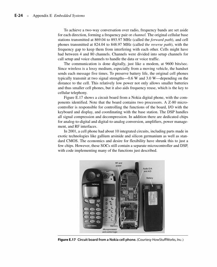
Figure E.17 shows a circuit board from a Nokia digital phone, with the com-ponents identified. Note that the board contains two processors. A Z-80 micro-controller is responsible for controlling the functions of the board, I/O with thekeyboard and display, and coordinating with the base station. The DSP handlesall signal compression and decompression. In addition there are dedicated chipsfor analog-to-digital and digital-to-analog conversion, amplifiers, power manage-ment, and RF interfaces.
In 2001, a cell phone had about 10 integrated circuits, including parts made inexotic technologies like gallium arsinide and silicon germanium as well as stan-dard CMOS. The economics and desire for flexibility have shrunk this to just afew chips. However, these SOCs still contain a separate microcontroller and DSP,with code implementing many of the functions just described.
Figure E.17 Circuit board from a Nokia cell phone. (Courtesy HowStuffWorks, Inc.)
RF andpower
Audio D/Aand A/D
Battery
Memory
Microprocessorand control logic
E.8 Concluding Remarks ■ E-25
Cell Phone Standards and Evolution
Improved communication speeds for cell phones were developed with multiplestandards. Code division multiple access (CDMA), as one popular example, usesa wider radio frequency band for a path than the original cell phones, calledadvanced mobile phone service (AMPS), a mostly analog system. The wider fre-quency makes it more difficult to block and is called spread spectrum. Otherstandards are time division multiple access (TDMA) and global system for mobilecommunication (GSM). These second-generation standards––CDMA, GSM, andTDMA––are mostly digital.
The big difference for CDMA is that all callers share the same channel, whichoperates at a much higher rate, and it then distinguishes the different calls byencoding each one uniquely. Each CDMA phone call starts at 9600 bits/sec; it isthen encoded and transmitted as equal-sized messages at 1.25 Mbits/sec. Ratherthan send each signal five times as in AMPS, each bit is stretched so that it takes11 times the minimum frequency, thereby accommodating interference and yetsuccessful transmission. The base station receives the messages, and it separatesthem into the separate 9600 bit/sec streams for each call.
To enhance privacy, CDMA uses pseudorandom sequences from a set of 64predefined codes. To synchronize the handset and base station so as to pick acommon pseudorandom seed, CDMA relies on a clock from the Global Position-ing System, which continuously transmits an accurate time signal. By carefullyselecting the codes, the shared traffic sounds like random noise to the listener.Hence, as more users share a channel there is more noise, and the signal-to-noiseratio gradually degrades. Thus, the capacity of the CDMA system is a matter oftaste, depending upon the sensitivity of the listener to background noise.
In addition, CDMA uses speech compression and varies the rate of data trans-ferred depending upon how much activity is going on in the call. Both these tech-niques preserve bandwidth, which allows for more calls per cell. CDMA mustregulate power carefully so that signals near the cell tower do not overwhelmthose from far away, with the goal of all signals reaching the tower at about thesame level. The side benefit is that CDMA handsets emit less power, which bothhelps battery life and increases capacity when users are close to the tower.
Thus, compared to AMPS, CDMA improves the capacity of a system by upto an order of magnitude, has better call quality, has better battery life, andenhances users’ privacy. After considerable commercial turmoil, there is a newthird-generation standard called International Mobile Telephony 2000 (IMT-2000), based primarily on two competing versions of CDMA and one TDMA.This standard may lead to cell phones that work anywhere in the world.
Embedded systems are a very broad category of computing devices. This appen-dix has shown just some aspects of this. For example, the TI 320C55 DSP is arelatively “RISC-like” processor designed for embedded applications, with very
E.8 Concluding Remarks
E-26 ■ Appendix E Embedded Systems
fine-tuned capabilities. On the other end of the spectrum, the TI 320C64x is avery high-performance, eight-issue VLIW processor for very demanding tasks.Some processors must operate on battery power alone; others have the luxury ofbeing plugged into line current. Unifying all of these is a need to perform somelevel of signal processing for embedded applications. Media extensions attemptto merge DSPs with some more general-purpose processing abilities to makethese processors usable for signal processing applications. We examined severalcase studies, including the Sony PlayStation 2, digital cameras, and cell phones.The PS2 performs detailed three-dimensional graphics, whereas a cell phoneencodes and decodes signals according to elaborate communication standards.But both have system architectures that are very different from general-purposedesktop or server platforms. In general, architectural decisions that seem practi-cal for general-purpose applications, such as multiple levels of caching or out-of-order superscalar execution, are much less desirable in embedded applications.This is due to chip area, cost, power, and real-time constraints. The programmingmodel that these systems present places more demands on both the programmerand the compiler for extracting parallelism.
Related Documents