Design and Simulation of SIGMA DELTA ADC EE435: VLSI By Trieu Nguyen, Quianqian Wang , Yunting Yin

Welcome message from author
This document is posted to help you gain knowledge. Please leave a comment to let me know what you think about it! Share it to your friends and learn new things together.
Transcript
Design and Simulation of SIGMA DELTA ADC EE435: VLSI By Trieu Nguyen, Quianqian Wang , Yunting Yin
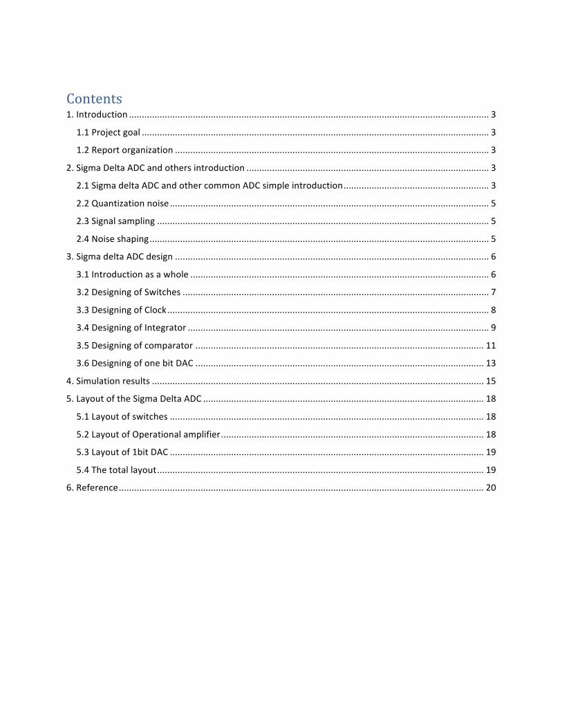
Contents 1. Introduction ............................................................................................................................................. 3
1.1 Project goal ........................................................................................................................................ 3
1.2 Report organization ........................................................................................................................... 3
2. Sigma Delta ADC and others introduction ............................................................................................... 3
2.1 Sigma delta ADC and other common ADC simple introduction......................................................... 3
2.2 Quantization noise............................................................................................................................. 5
2.3 Signal sampling .................................................................................................................................. 5
2.4 Noise shaping..................................................................................................................................... 5
3. Sigma delta ADC design ........................................................................................................................... 6
3.1 Introduction as a whole ..................................................................................................................... 6
3.2 Designing of Switches ........................................................................................................................ 7
3.3 Designing of Clock.............................................................................................................................. 8
3.4 Designing of Integrator ...................................................................................................................... 9
3.5 Designing of comparator ................................................................................................................. 11
3.6 Designing of one bit DAC ................................................................................................................. 13
4. Simulation results .................................................................................................................................. 15
5. Layout of the Sigma Delta ADC .............................................................................................................. 18
5.1 Layout of switches ........................................................................................................................... 18
5.2 Layout of Operational amplifier....................................................................................................... 18
5.3 Layout of 1bit DAC ........................................................................................................................... 19
5.4 The total layout................................................................................................................................ 19
6. Reference............................................................................................................................................... 20
1. Introduction 1.1 Project goal In this project, we are asked to design an ADC or DAC that is an 8-‐bit to 10-‐bit. In our design, we use the sigma delta to achieve this goal.
1.2 Report organization In our report, we first introduce the sigma delta ADC and the reason why we use this structure. Next, we will explain how many parts in our design specifically and we would provide their structures and how they work. Thirdly, we would provide detailed value of parameters of different transistors, resistors and capacitors that make of these components.
2. Sigma Delta ADC and others introduction 2.1 Sigma delta ADC and other common ADC simple introduction In this project, we choose sigma delta ADC. As for the reasons, first, the requirements ask us to build a 10-‐bit ADC or DAC, the normal R-‐2R DAC would have too much resistors and even we separate it into two steps. Except that, the current steering DAC have the same problem, and if we don’t include the binary to thermometer decoder, the DAC would have large DNL, which means the DAC would not have high accuracy and consider that we need to build 10-‐bit DAC. As a result, the value of bit is too high for the current steering DAC. In the sigma delta ADC, it will save more space than any other ADCs. Secondly, the delta sigma would save more space and power dissipation, because it just mainly consists a comparator, an integrator and a 1-‐bit DAC. Besides, it just has three main components, which means have few parts to be supplied large power.
As for the working principle of sigma delta ADC, it use the oversampling to reduce the quantization noise that can improve the effective number of bits and the specific methods and equations would be provide in the later report.
After here, we would introduce some kinds of simple architecture of ADCs.
Flash ADC:
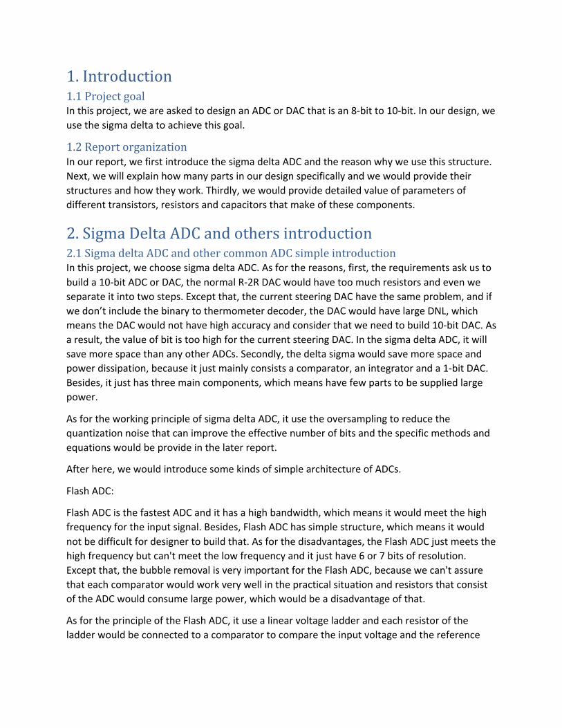
Flash ADC is the fastest ADC and it has a high bandwidth, which means it would meet the high frequency for the input signal. Besides, Flash ADC has simple structure, which means it would not be difficult for designer to build that. As for the disadvantages, the Flash ADC just meets the high frequency but can't meet the low frequency and it just have 6 or 7 bits of resolution. Except that, the bubble removal is very important for the Flash ADC, because we can't assure that each comparator would work very well in the practical situation and resistors that consist of the ADC would consume large power, which would be a disadvantage of that.
As for the principle of the Flash ADC, it use a linear voltage ladder and each resistor of the ladder would be connected to a comparator to compare the input voltage and the reference
voltage. After that, these signals would go into a digital thermometer code and then would go into the thermometer code to binary code to make it convert to binary code.
The basic structure is more like the figure below.
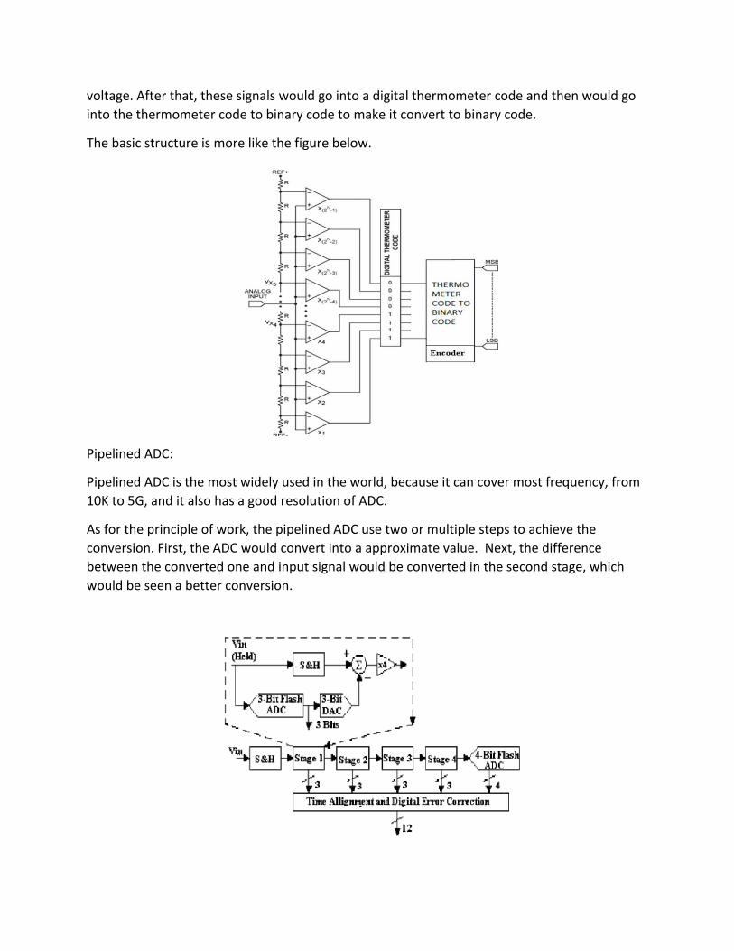
Pipelined ADC:
Pipelined ADC is the most widely used in the world, because it can cover most frequency, from 10K to 5G, and it also has a good resolution of ADC.
As for the principle of work, the pipelined ADC use two or multiple steps to achieve the conversion. First, the ADC would convert into a approximate value. Next, the difference between the converted one and input signal would be converted in the second stage, which would be seen a better conversion.
Figure 1 Architecture of Flash ADC
Figure 2 Architecture of Pipe Line ADC
The figure above is about the 12 bits pipeline ADC.
2.2 Quantization noise Because the analog signal is continuous and the digital signal is discrete, there would produce some difference when the data conversion happens. And this difference would cause distortion, which is the quantization noise. As for the quantization error, it is the converts can’t work normally.
2.3 Signal sampling In Sigma delta ADC, there is oversampling to reduce the quantization noise. Oversampling the input signal means that sample the frequency at a higher frequency. Besides, there would be a new relationship about the noise shaping.
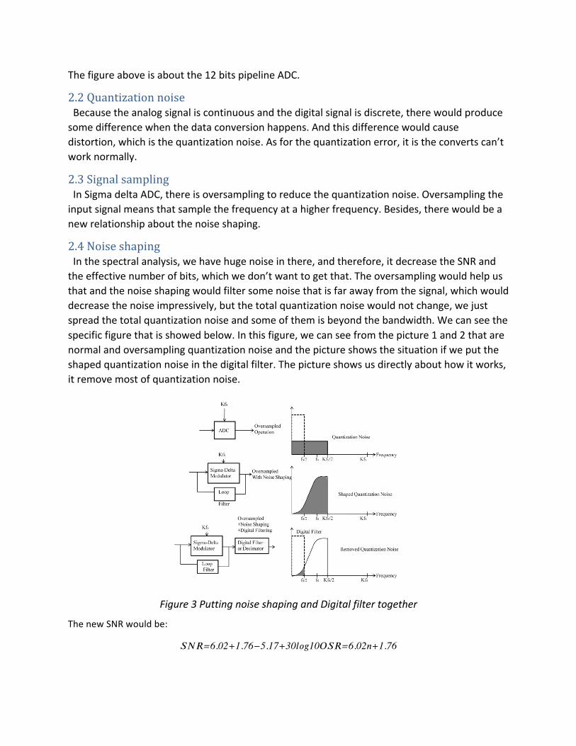
2.4 Noise shaping In the spectral analysis, we have huge noise in there, and therefore, it decrease the SNR and the effective number of bits, which we don’t want to get that. The oversampling would help us that and the noise shaping would filter some noise that is far away from the signal, which would decrease the noise impressively, but the total quantization noise would not change, we just spread the total quantization noise and some of them is beyond the bandwidth. We can see the specific figure that is showed below. In this figure, we can see from the picture 1 and 2 that are normal and oversampling quantization noise and the picture shows the situation if we put the shaped quantization noise in the digital filter. The picture shows us directly about how it works, it remove most of quantization noise.
Figure 3 Putting noise shaping and Digital filter together
The new SNR would be:
𝑆𝑁𝑅=6.02+1.76−5.17+30𝑙𝑜𝑔10𝑂𝑆𝑅=6.02𝑛+1.76
According to this equation, we can get the SNR of this ADC and we also can get the effective number of bits. Besides, the OSR in there means the oversampling rate.
𝑂𝑆𝑅=𝑓𝑠2𝑓0
3. Sigma delta ADC design 3.1 Introduction as a whole
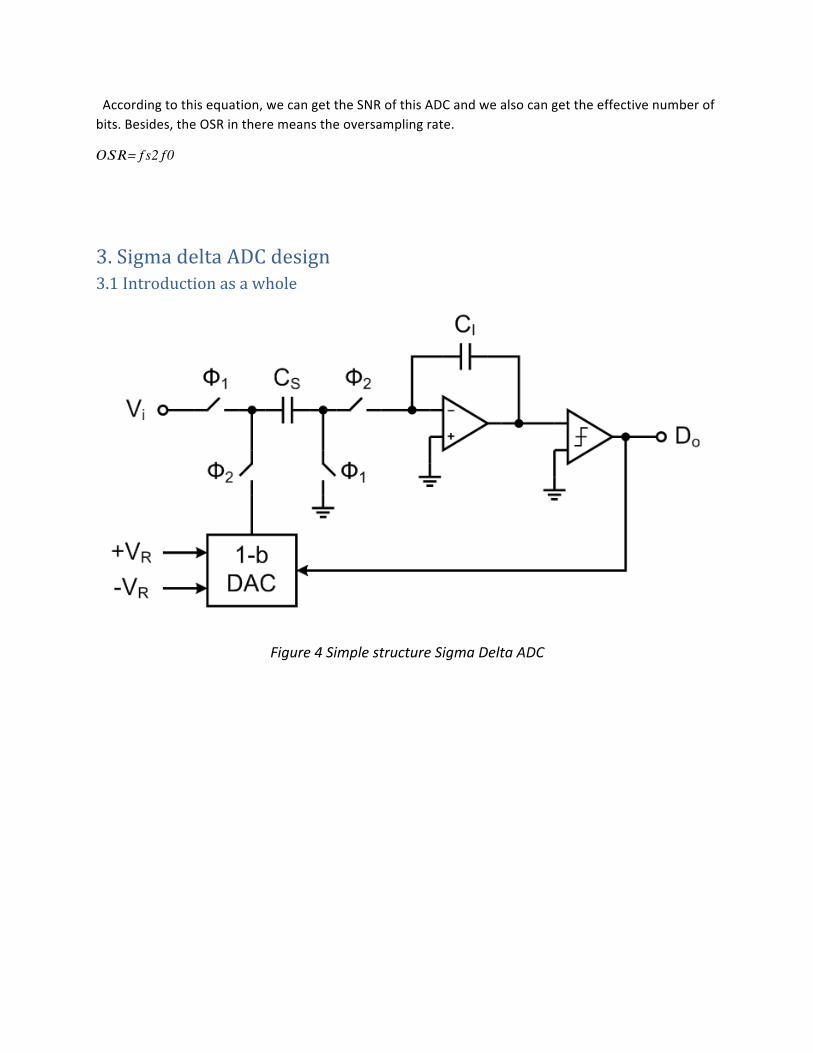
Figure 4 Simple structure Sigma Delta ADC
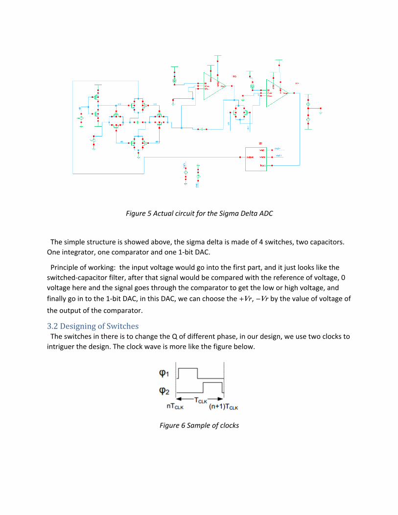
Figure 5 Actual circuit for the Sigma Delta ADC
The simple structure is showed above, the sigma delta is made of 4 switches, two capacitors. One integrator, one comparator and one 1-‐bit DAC.
Principle of working: the input voltage would go into the first part, and it just looks like the switched-‐capacitor filter, after that signal would be compared with the reference of voltage, 0 voltage here and the signal goes through the comparator to get the low or high voltage, and finally go in to the 1-‐bit DAC, in this DAC, we can choose the +𝑉𝑟, −𝑉𝑟 by the value of voltage of the output of the comparator.
3.2 Designing of Switches The switches in there is to change the Q of different phase, in our design, we use two clocks to intriguer the design. The clock wave is more like the figure below.
Figure 6 Sample of clocks
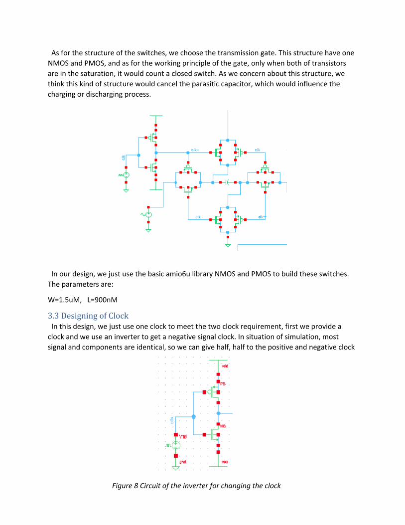
As for the structure of the switches, we choose the transmission gate. This structure have one NMOS and PMOS, and as for the working principle of the gate, only when both of transistors are in the saturation, it would count a closed switch. As we concern about this structure, we think this kind of structure would cancel the parasitic capacitor, which would influence the charging or discharging process.
In our design, we just use the basic amio6u library NMOS and PMOS to build these switches. The parameters are:
W=1.5uM, L=900nM
3.3 Designing of Clock In this design, we just use one clock to meet the two clock requirement, first we provide a clock and we use an inverter to get a negative signal clock. In situation of simulation, most signal and components are identical, so we can give half, half to the positive and negative clock
Figure 7 Circuit of switches
Figure 8 Circuit of the inverter for changing the clock
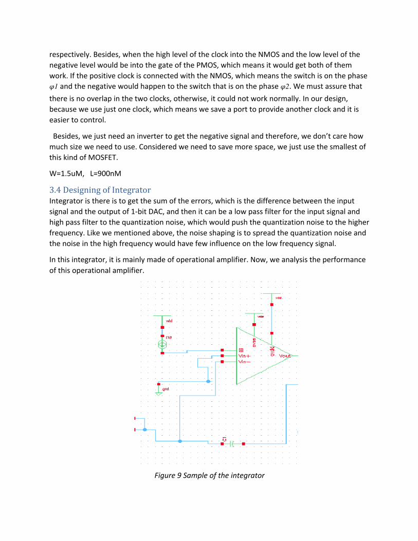
respectively. Besides, when the high level of the clock into the NMOS and the low level of the negative level would be into the gate of the PMOS, which means it would get both of them work. If the positive clock is connected with the NMOS, which means the switch is on the phase 𝜑1 and the negative would happen to the switch that is on the phase 𝜑2. We must assure that
there is no overlap in the two clocks, otherwise, it could not work normally. In our design, because we use just one clock, which means we save a port to provide another clock and it is easier to control.
Besides, we just need an inverter to get the negative signal and therefore, we don’t care how much size we need to use. Considered we need to save more space, we just use the smallest of this kind of MOSFET.
W=1.5uM, L=900nM
3.4 Designing of Integrator Integrator is there is to get the sum of the errors, which is the difference between the input signal and the output of 1-‐bit DAC, and then it can be a low pass filter for the input signal and high pass filter to the quantization noise, which would push the quantization noise to the higher frequency. Like we mentioned above, the noise shaping is to spread the quantization noise and the noise in the high frequency would have few influence on the low frequency signal.
In this integrator, it is mainly made of operational amplifier. Now, we analysis the performance of this operational amplifier.
Figure 9 Sample of the integrator
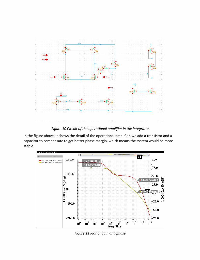
Figure 10 Circuit of the operational amplifier in the integrator
In the figure above, it shows the detail of the operational amplifier, we add a transistor and a capacitor to compensate to get better phase margin, which means the system would be more stable.
Figure 11 Plot of gain and phase
The figure shows that the gain is 74dB and the phase margin of this operational amplifier is 54.25, which means this operational amplifier has a good gain and is a sable system.
The parameters of this operational amplifier is shown below
All sizes in the first stage is same 𝑊1𝐿1=9𝑢600𝑛=606
The three bias sizes are same 𝑊𝑏𝐿𝑏=9𝑢600𝑛=808
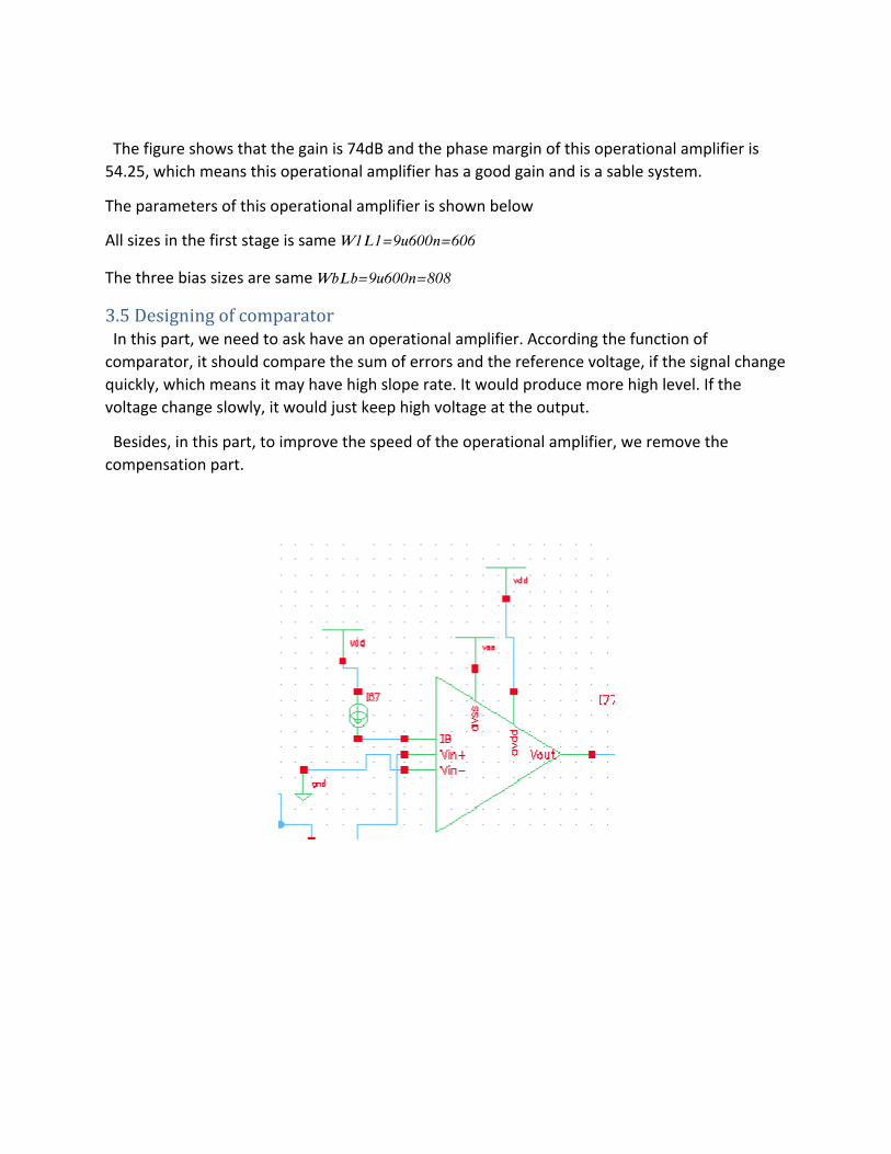
3.5 Designing of comparator In this part, we need to ask have an operational amplifier. According the function of comparator, it should compare the sum of errors and the reference voltage, if the signal change quickly, which means it may have high slope rate. It would produce more high level. If the voltage change slowly, it would just keep high voltage at the output.
Besides, in this part, to improve the speed of the operational amplifier, we remove the compensation part.
Figure 12 Sample of the comparator
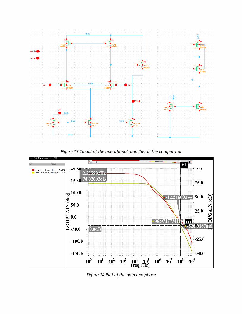
Figure 13 Circuit of the operational amplifier in the comparator
Figure 14 Plot of the gain and phase
In the figure we can see that, the phase margin is negative, but we don’t need the stable system, we just need the fast, high gain, large GWB comparator.
The parameters:
The value of parameters are almost same with the amplifier that we use to build the integrator.
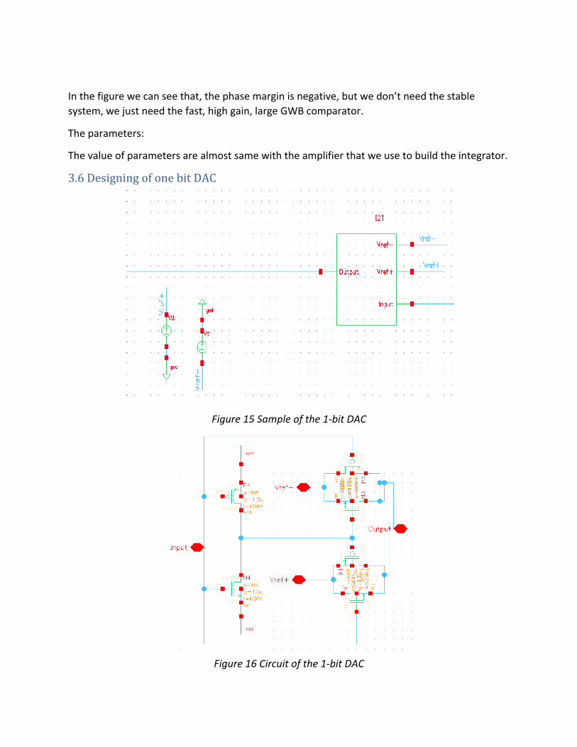
3.6 Designing of one bit DAC
Figure 15 Sample of the 1-‐bit DAC
Figure 16 Circuit of the 1-‐bit DAC
In this one bit DAC, we can see the if the input voltage goes through a push-‐pull inverter, if the value of input signal is between −𝑉𝑟, and +𝑉𝑟, it would connect the two transistors above the circuit, providing output signal of −𝑉𝑟 and if value of input signal is bigger than +𝑉𝑟, it would connect the two transistors below , producing the output signal of +𝑉𝑟.
The parameters of two transistors in the inverter is the small size of this kind of transistor. Besides, the rest of this circuit are two transmission gates and therefore, their sizes are all the smallest sizes.
W=1.5uM, L=900nM
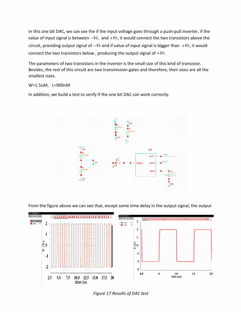
In addition, we build a test to verify if the one bit DAC can work correctly.
From the figure above we can see that, except some time delay in the output signal, the output Figure 18 Test Circuit of 1-‐bit DAC
Figure 17 Results of DAC test
signal almost have same voltage level with the input signal, which means this circuit can work correctly.
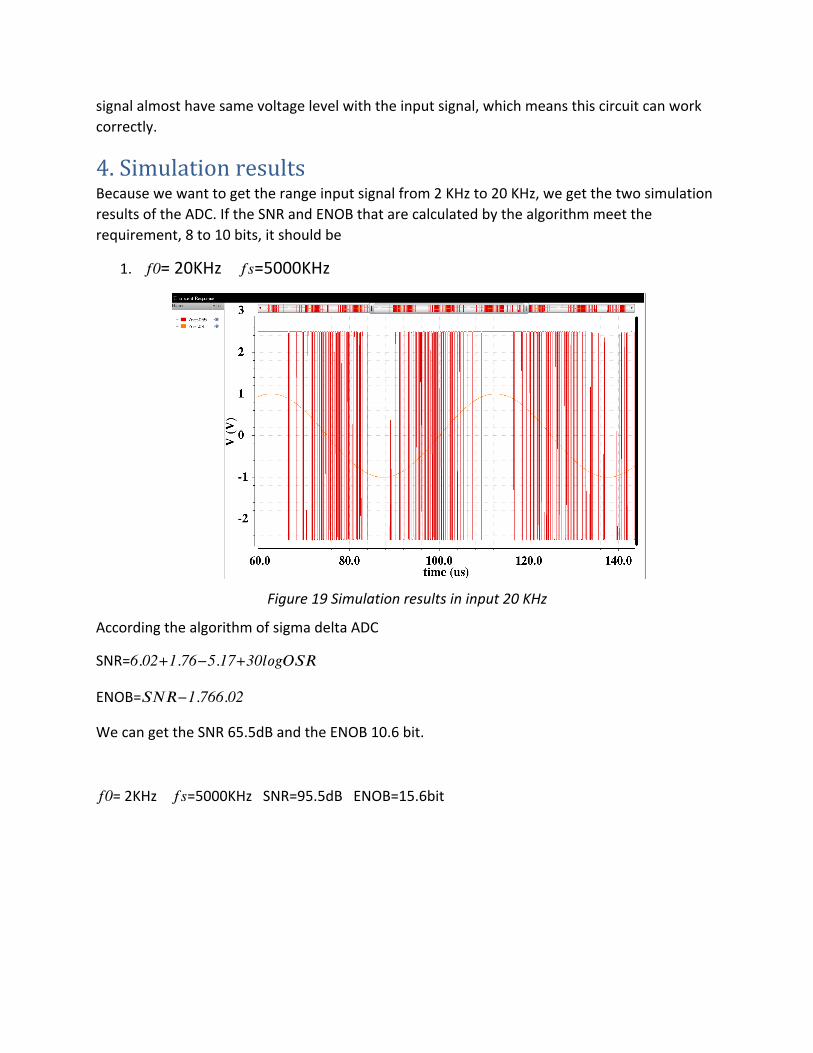
4. Simulation results Because we want to get the range input signal from 2 KHz to 20 KHz, we get the two simulation results of the ADC. If the SNR and ENOB that are calculated by the algorithm meet the requirement, 8 to 10 bits, it should be
1. 𝑓0= 20KHz 𝑓𝑠=5000KHz
Figure 19 Simulation results in input 20 KHz
According the algorithm of sigma delta ADC
SNR=6.02+1.76−5.17+30𝑙𝑜𝑔𝑂𝑆𝑅
ENOB=𝑆𝑁𝑅−1.766.02
We can get the SNR 65.5dB and the ENOB 10.6 bit.
𝑓0= 2KHz 𝑓𝑠=5000KHz SNR=95.5dB ENOB=15.6bit
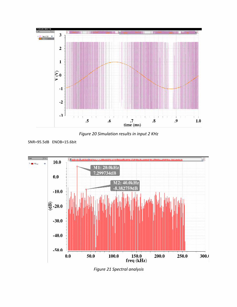
Figure 20 Simulation results in input 2 KHz
SNR=95.5dB ENOB=15.6bit
Figure 21 Spectral analysis

From the figure above we can see the fundamental signal and other harmonics, we provide the magnitude of fundamental and second harmonic. As a result, we can get the SFDR is:
SFDR=7.3-‐(-‐8.38) =15.68dB
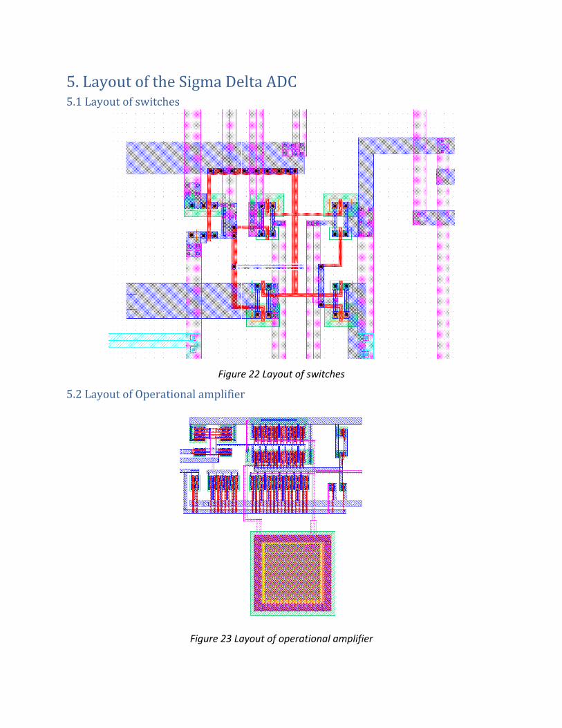
5. Layout of the Sigma Delta ADC 5.1 Layout of switches
Figure 22 Layout of switches
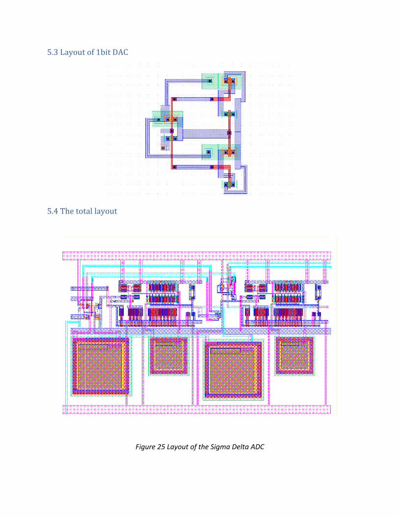
5.2 Layout of Operational amplifier
Figure 23 Layout of operational amplifier
5.3 Layout of 1bit DAC
5.4 The total layout
Figure 25 Layout of the Sigma Delta ADC
Figure 24 Layout of 1-‐bit DAC
6. Reference
[1] SoumyaSuravita Guru. ”Design and Simulation of SIGMA DELTA ADC” [2] Hao Meng.”Sigma Delta ADC” [3] Nawshad Amin, Goh chit Guan and Ibrahim Ahmad.“An Efficient First order Sigma Delta modulator Design” [4] P. M. Aziz, H. V. Sorensen, & J. V. Spiegel, “An Overview of Sigma-DeltaConverters”, IEEE Signal Processing Magazine, pp.61-84, Jan. 1996.
Related Documents