RT8553A ® © Copyright 2015 Richtek Technology Corporation. All rights reserved. is a registered trademark of Richtek Technology Corporation. DS8553A-00 January 2015 www.richtek.com 1 Applications Cellular Phones Digital Cameras PDAs and Smart Phones Probable Instruments Dual-Output Synchronous DC/DC Converter General Description The RT8553A is a dual-output DC/DC converter which is designed to provide the power for consumer products. It integrates a Boost converter and an inverting-Boost converter for enhancing the overall system efficiency of battery powered products. The RT8553A operates in Forced CCM mode for light load and heavy load condition. The high frequency allows for reduction of external components. In shutdown mode, the RT8553A consumes less than 1μA current. The RT8553A provides soft-start, OCP, OTP, OVP and UVLO function. The RT8553A is available in the tiny UDFN-12L 3x3 package to achieve best solution for saving PCB space and total BOM cost saving considerations. Features Boost Converter to Supply Positive Voltage from 4.6V to 5.4V Through External Feedback Resistors Buck-Boost Converter to Supply Negative Voltage from −4.6V to −5.4V Through External Feedback Resistors Maximum Output Current up to 200mA Typical Efficiency : 85% PWM Mode @ 1.5MHz Switching Frequency High Output Voltage Accuracy Excellent Line and Load Transient Excellent Line and Load Regulation Soft-Start to Limit Inrush Current Over-Temperature Protection (OTP) Over-Current Protection (OCP) Over-Voltage Protection (OVP) Low Quiescent Current < 1μA in Shutdown Mode RoHS Compliant and Halogen Free Simplified Application Circuit Ordering Information Note : Richtek products are : RoHS compliant and compatible with the current require- ments of IPC/JEDEC J-STD-020. Suitable for use in SnPb or Pb-free soldering processes. Package Type QU : UDFN-12L 3x3 (U-Type) RT8553A Lead Plating System G : Green (Halogen Free and Pb Free) VINP LX1 VOUT2 V IN PGND RT8553A C IN1 L1 VINA EN VOUT1 C OUT1 V OUT1 LX2 L2 AGND Enable R1 R2 C OUT2 V OUT2 R3 R4 FB1 FB2 VREF GND C IN2

Welcome message from author
This document is posted to help you gain knowledge. Please leave a comment to let me know what you think about it! Share it to your friends and learn new things together.
Transcript
RT8553A®
©Copyright 2015 Richtek Technology Corporation. All rights reserved. is a registered trademark of Richtek Technology Corporation.
DS8553A-00 January 2015 www.richtek.com1
Applications Cellular Phones
Digital Cameras
PDAs and Smart Phones
Probable Instruments
Dual-Output Synchronous DC/DC Converter
General Description
The RT8553A is a dual-output DC/DC converter which is
designed to provide the power for consumer products. It
integrates a Boost converter and an inverting-Boost
converter for enhancing the overall system efficiency of
battery powered products. The RT8553A operates in
Forced CCM mode for light load and heavy load condition.
The high frequency allows for reduction of external
components. In shutdown mode, the RT8553A consumes
less than 1μA current. The RT8553A provides soft-start,
OCP, OTP, OVP and UVLO function. The RT8553A is
available in the tiny UDFN-12L 3x3 package to achieve
best solution for saving PCB space and total BOM cost
saving considerations.
Features Boost Converter to Supply Positive Voltage from
4.6V to 5.4V Through External Feedback Resistors
Buck-Boost Converter to Supply Negative Voltage
from −−−−−4.6V to −−−−−5.4V Through External Feedback
Resistors
Maximum Output Current up to 200mA
Typical Efficiency : 85%
PWM Mode @ 1.5MHz Switching Frequency
High Output Voltage Accuracy
Excellent Line and Load Transient
Excellent Line and Load Regulation
Soft-Start to Limit Inrush Current
Over-Temperature Protection (OTP)
Over-Current Protection (OCP)
Over-Voltage Protection (OVP)
Low Quiescent Current < 1μμμμμA in Shutdown Mode
RoHS Compliant and Halogen Free
Simplified Application Circuit
Ordering Information
Note :
Richtek products are :
RoHS compliant and compatible with the current require-
ments of IPC/JEDEC J-STD-020.
Suitable for use in SnPb or Pb-free soldering processes.
Package TypeQU : UDFN-12L 3x3 (U-Type)
RT8553A
Lead Plating SystemG : Green (Halogen Free and Pb Free)
VINP LX1
VOUT2
VIN
PGND
RT8553A
CIN1
L1
VINA
EN
VOUT1COUT1
VOUT1
LX2L2
AGND
EnableR1
R2
COUT2
VOUT2
R3
R4
FB1
FB2
VREF
GND
CIN2
RT8553A
2
DS8553A-00 January 2015www.richtek.com
©Copyright 2015 Richtek Technology Corporation. All rights reserved. is a registered trademark of Richtek Technology Corporation.
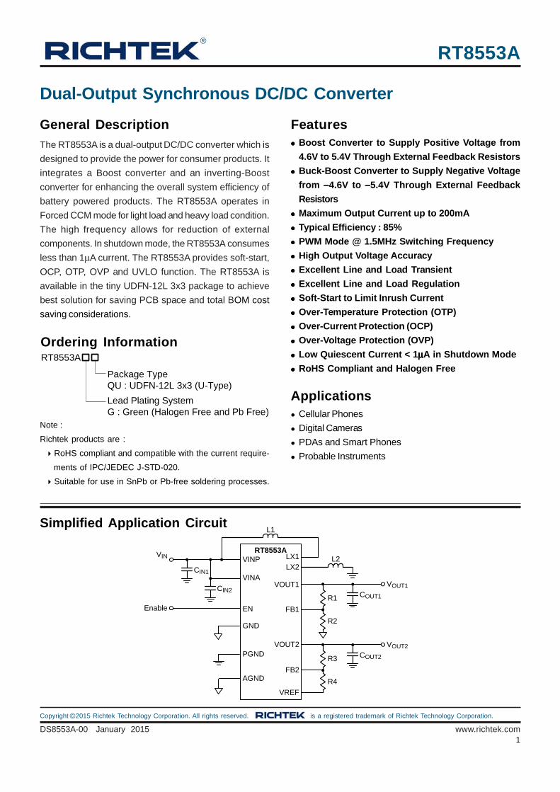
Functional Pin DescriptionPin No. Pin Name Pin Function
1 LX1 Switch Node of Boost Converter.
2 VOUT1 Boost Converter Output.
3 PGND Power Ground.
4 FB1 Feedback Voltage Input of Boost Converter.
5 AGND Analog Ground.
6 EN Enable Control Input. (Active High)
7 VINA Analog Supply Voltage Input.
8 VREF Reference Voltage.
9 FB2 Feedback Voltage Input of Inverting Boost Converter.
10 VOUT2 Buck-Boost Converter Output.
11 LX2 Switch Node of Buck-Boost Converter.
12 VINP Power Supply Voltage Input.
13 (Exposed Pad) GND Ground. The exposed pad must be soldered to a large PCB and connected to AGND for maximum power dissipation.
Pin Configurations(TOP VIEW)
UDFN-12L 3x3
Marking Information3S= : Product Code
YMDNN : Date Code3S=YMDNN
LX1VOUT1
AGNDFB1
VINPLX2VOUT2
VREFFB2
PGND
EN VINA
11
109
12345
12
6 78
GN
D
13
RT8553A
3
DS8553A-00 January 2015 www.richtek.com
©Copyright 2015 Richtek Technology Corporation. All rights reserved. is a registered trademark of Richtek Technology Corporation.
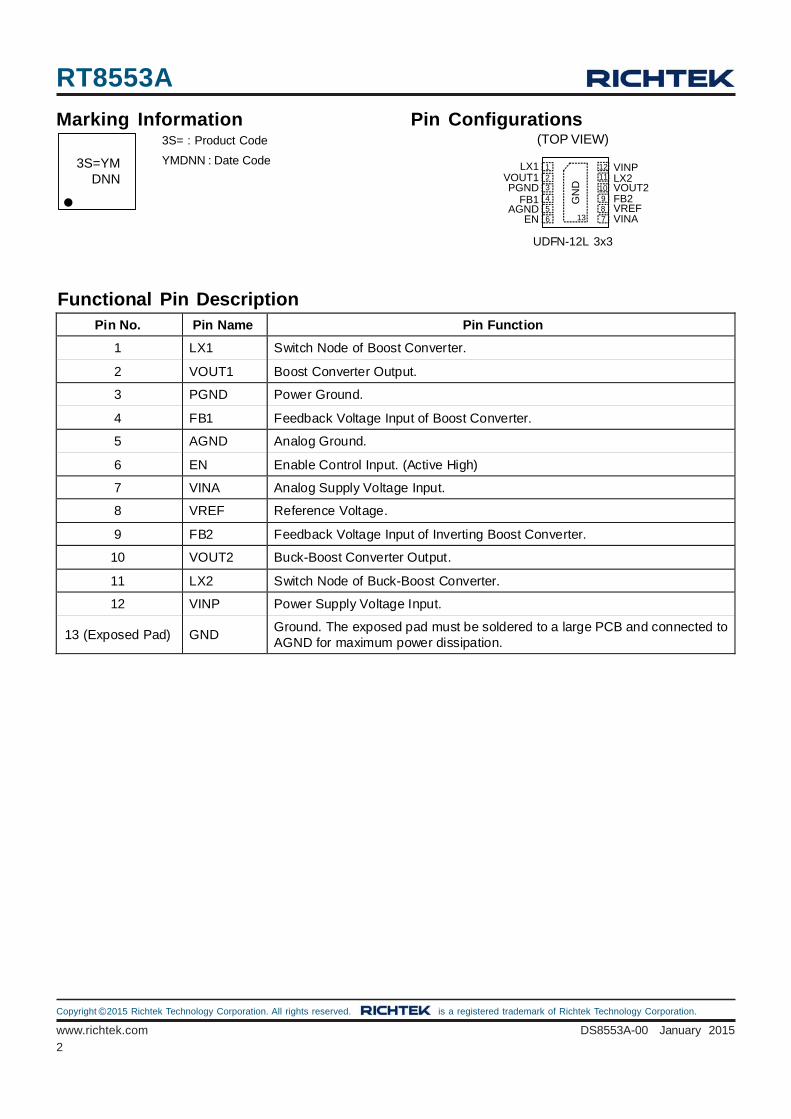
Function Block Diagram
Operation
The RT8553A is a dual-output synchronous DC/DC
converter for consumer product applications that it can
support input voltage range from 2.5V to 4.5V and the
output current up to 200mA. The RT8553A uses current
mode architecture for the purpose of high efficiency and
high transient response. The VOUT1 positive output voltage
is produced from the DC/DC Boost converter, and output
voltage can be adjusted by external feedback resistors.
The VOUT2 negative output voltage is produced from the
DC/DC Buck-Boost converter, and the negative output
voltage can be adjusted by external feedback resistors.
When the EN goes high, the positive output voltage will
be enabled with an internal soft-start process. After the
positive output voltage is ready, negative output voltage
will be enabled with an internal soft-start process.
The RT8553A provides protection functions, such as Over-
Current Protection (OCP), Over-Temperature Protection
(OTP) and Over-Voltage Protection (OVP) to protect
application products and itself. The RT8553A employs an
internal soft-start feature to avoid high inrush currents
during start-up. Both the Boost and the Buck-Boost
converters can operate in Force Continuous Conduction
Mode (FCCM) for better stability and minimum output
ripple.
Switching Well
+
OCP2
N2
N1
P1
OVP1
VOUT1
LX2Band GapReference
VINP
VINA
AGND
LX1
PWMLogic
+
-
VIN Detection
OCP1
+
-GM
VREF1
P2
OVP2
PWMLogic
VOUT2
+ +
-
+
-GM
VREF2Oscillator
VREF
Soft-StartEN
VINP
PGND
UVLO
OTP
FB1
FB2
RT8553A
4
DS8553A-00 January 2015www.richtek.com
©Copyright 2015 Richtek Technology Corporation. All rights reserved. is a registered trademark of Richtek Technology Corporation.
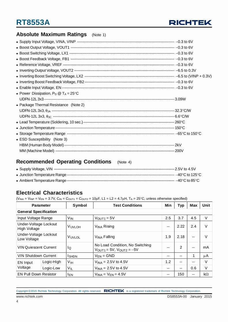
Electrical Characteristics(VINA = VINP = VEN = 3.7V, CIN = COUT1 = COUT2 = 10μF, L1 = L2 = 4.7μH, TA = 25°C, unless otherwise specified)
Absolute Maximum Ratings (Note 1)
Supply Input Voltage, VINA, VINP ----------------------------------------------------------------------------- −0.3 to 6V
Boost Output Voltage, VOUT1 ---------------------------------------------------------------------------------- −0.3 to 6V
Boost Switching Voltage, LX1 ----------------------------------------------------------------------------------- −0.3 to 6V
Boost Feedback Voltage, FB1 ---------------------------------------------------------------------------------- −0.3 to 6V
Reference Voltage, VREF ---------------------------------------------------------------------------------------- −0.3 to 6V
Inverting Output Voltage, VOUT2 ------------------------------------------------------------------------------- −6.5 to 0.3V
Inverting Boost Switching Voltage, LX2 ----------------------------------------------------------------------- −6.5 to (VINP + 0.3V)
Inverting Boost Feedback Voltage, FB2 ----------------------------------------------------------------------- −0.3 to 6V
Enable Input Voltage, EN ----------------------------------------------------------------------------------------- −0.3 to 6V
Power Dissipation, PD @ TA = 25°C
UDFN-12L 3x3-------------------------------------------------------------------------------------------------------3.09W
Package Thermal Resistance (Note 2)
UDFN-12L 3x3, θJA -------------------------------------------------------------------------------------------------32.3°C/W
UDFN-12L 3x3, θJC ------------------------------------------------------------------------------------------------ 6.6°C/W
Lead Temperature (Soldering, 10 sec.) ------------------------------------------------------------------------ 260°C Junction Temperature ---------------------------------------------------------------------------------------------- 150°C Storage Temperature Range ------------------------------------------------------------------------------------- −65°C to 150°C ESD Susceptibility (Note 3)
HBM (Human Body Model) --------------------------------------------------------------------------------------- 2kV
MM (Machine Model) ----------------------------------------------------------------------------------------------200V
Recommended Operating Conditions (Note 4)
Supply Voltage, VIN ----------------------------------------------------------------------------------------------- 2.5V to 4.5V
Junction Temperature Range------------------------------------------------------------------------------------- −40°C to 125°C Ambient Temperature Range------------------------------------------------------------------------------------- −40°C to 85°C
Parameter Symbol Test Conditions Min Typ Max Unit
General Specification
Input Voltage Range VIN VOUT1 = 5V 2.5 3.7 4.5 V
Under-Voltage Lockout High Voltage
VUVLOH VINA Rising -- 2.22 2.4 V
Under-Voltage Lockout Low Voltage
VUVLOL VINA Falling 1.9 2.18 -- V
VIN Quiescent Current IQ No Load Condition, No Switching VOUT1 = 5V, VOUT2 = 5V
-- 2 -- mA
VIN Shutdown Current ISHDN VEN = GND -- -- 1 A
EN Input Voltage
Logic-High VIH VINA = 2.5V to 4.5V 1.2 -- -- V
Logic-Low VIL VINA = 2.5V to 4.5V -- -- 0.6 V
EN Pull Down Resistor IEN VINA = VEN = 4.5V -- 150 -- k
RT8553A
5
DS8553A-00 January 2015 www.richtek.com
©Copyright 2015 Richtek Technology Corporation. All rights reserved. is a registered trademark of Richtek Technology Corporation.
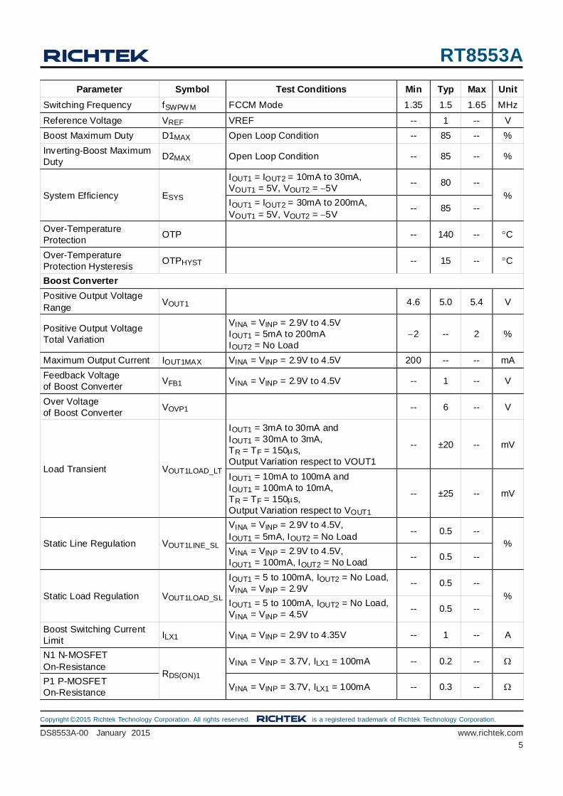
Parameter Symbol Test Conditions Min Typ Max Unit
Switching Frequency fSWPW M FCCM Mode 1.35 1.5 1.65 MHz
Reference Voltage VREF VREF -- 1 -- V
Boost Maximum Duty D1MAX Open Loop Condition -- 85 -- %
Inverting-Boost Maximum Duty
D2MAX Open Loop Condition -- 85 -- %
System Efficiency ESYS
IOUT1 = IOUT2 = 10mA to 30mA, VOUT1 = 5V, VOUT2 = 5V
-- 80 --
% IOUT1 = IOUT2 = 30mA to 200mA, VOUT1 = 5V, VOUT2 = 5V
-- 85 --
Over-Temperature Protection
OTP -- 140 -- C
Over-Temperature Protection Hysteresis
OTPHYST -- 15 -- C
Boost Converter
Positive Output Voltage Range
VOUT1 4.6 5.0 5.4 V
Positive Output Voltage Total Variation
VINA = VINP = 2.9V to 4.5V IOUT1 = 5mA to 200mA IOUT2 = No Load
2 -- 2 %
Maximum Output Current IOUT1MAX VINA = VINP = 2.9V to 4.5V 200 -- -- mA
Feedback Voltage of Boost Converter
VFB1 VINA = VINP = 2.9V to 4.5V -- 1 -- V
Over Voltage of Boost Converter
VOVP1 -- 6 -- V
Load Transient VOUT1LOAD_LT
IOUT1 = 3mA to 30mA and IOUT1 = 30mA to 3mA, TR = TF = 150s, Output Variation respect to VOUT1
-- ±20 -- mV
IOUT1 = 10mA to 100mA and IOUT1 = 100mA to 10mA, TR = TF = 150s, Output Variation respect to VOUT1
-- ±25 -- mV
Static Line Regulation VOUT1LINE_SL
VINA = VINP = 2.9V to 4.5V, IOUT1 = 5mA, IOUT2 = No Load
-- 0.5 -- %
VINA = VINP = 2.9V to 4.5V, IOUT1 = 100mA, IOUT2 = No Load
-- 0.5 --
Static Load Regulation VOUT1LOAD_SL
IOUT1 = 5 to 100mA, IOUT2 = No Load, VINA = VINP = 2.9V
-- 0.5 --
% IOUT1 = 5 to 100mA, IOUT2 = No Load, VINA = VINP = 4.5V
-- 0.5 --
Boost Switching Current Limit
ILX1 VINA = VINP = 2.9V to 4.35V -- 1 -- A
N1 N-MOSFET On-Resistance
RDS(ON)1 VINA = VINP = 3.7V, ILX1 = 100mA -- 0.2 --
P1 P-MOSFET On-Resistance
VINA = VINP = 3.7V, ILX1 = 100mA -- 0.3 --
RT8553A
6
DS8553A-00 January 2015www.richtek.com
©Copyright 2015 Richtek Technology Corporation. All rights reserved. is a registered trademark of Richtek Technology Corporation.
Note 1. Stresses beyond those listed “Absolute Maximum Ratings” may cause permanent damage to the device. These are
stress ratings only, and functional operation of the device at these or any other conditions beyond those indicated in
the operational sections of the specifications is not implied. Exposure to absolute maximum rating conditions may
affect device reliability.
Note 2. θJA is measured at TA = 25°C on a high effective thermal conductivity four-layer test board per JEDEC 51-7. θJC is
measured at the exposed pad of the package.
Note 3. Devices are ESD sensitive. Handling precaution is recommended.
Note 4. The device is not guaranteed to function outside its operating conditions.
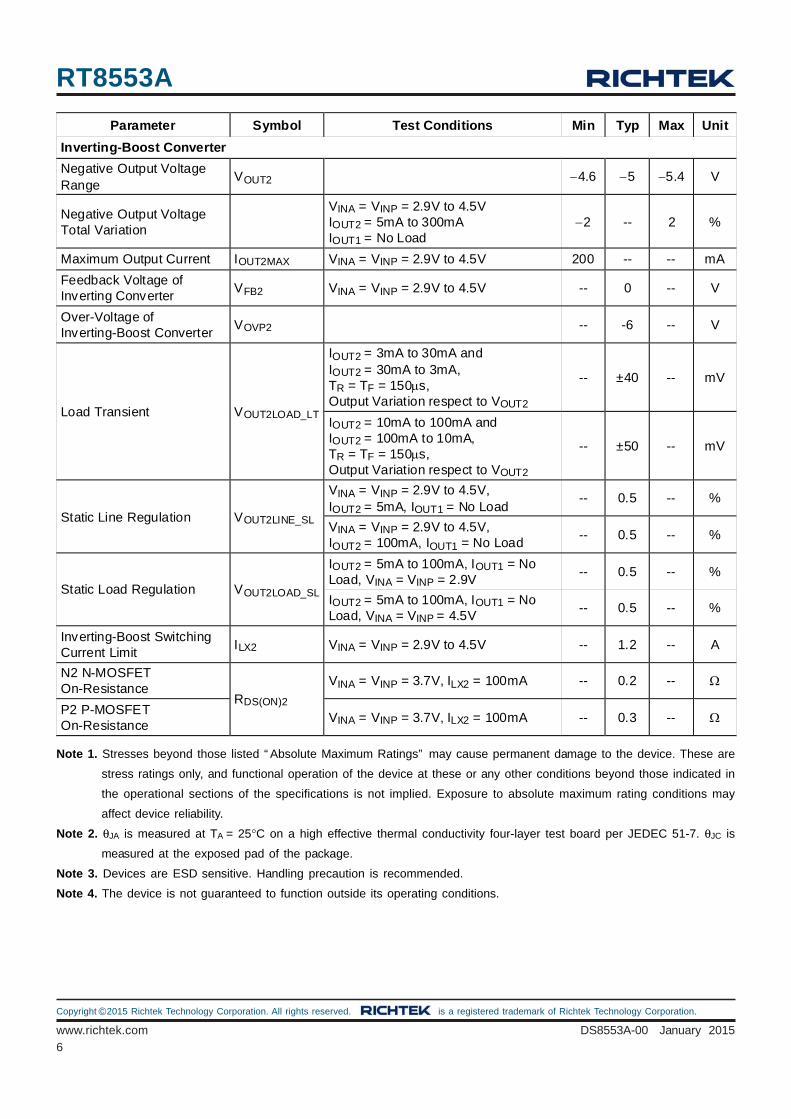
Parameter Symbol Test Conditions Min Typ Max Unit
Inverting-Boost Converter
Negative Output Voltage Range
VOUT2 4.6 5 5.4 V
Negative Output Voltage Total Variation
VINA = VINP = 2.9V to 4.5V IOUT2 = 5mA to 300mA IOUT1 = No Load
2 -- 2 %
Maximum Output Current IOUT2MAX VINA = VINP = 2.9V to 4.5V 200 -- -- mA
Feedback Voltage of Inverting Converter
VFB2 VINA = VINP = 2.9V to 4.5V -- 0 -- V
Over-Voltage of Inverting-Boost Converter
VOVP2 -- -6 -- V
Load Transient VOUT2LOAD_LT
IOUT2 = 3mA to 30mA and IOUT2 = 30mA to 3mA, TR = TF = 150s, Output Variation respect to VOUT2
-- ±40 -- mV
IOUT2 = 10mA to 100mA and IOUT2 = 100mA to 10mA, TR = TF = 150s, Output Variation respect to VOUT2
-- ±50 -- mV
Static Line Regulation VOUT2LINE_SL
VINA = VINP = 2.9V to 4.5V, IOUT2 = 5mA, IOUT1 = No Load
-- 0.5 -- %
VINA = VINP = 2.9V to 4.5V, IOUT2 = 100mA, IOUT1 = No Load
-- 0.5 -- %
Static Load Regulation VOUT2LOAD_SL
IOUT2 = 5mA to 100mA, IOUT1 = No Load, VINA = VINP = 2.9V
-- 0.5 -- %
IOUT2 = 5mA to 100mA, IOUT1 = No Load, VINA = VINP = 4.5V
-- 0.5 -- %
Inverting-Boost Switching Current Limit
ILX2 VINA = VINP = 2.9V to 4.5V -- 1.2 -- A
N2 N-MOSFET On-Resistance
RDS(ON)2
VINA = VINP = 3.7V, ILX2 = 100mA -- 0.2 --
P2 P-MOSFET On-Resistance
VINA = VINP = 3.7V, ILX2 = 100mA -- 0.3 --
RT8553A
7
DS8553A-00 January 2015 www.richtek.com
©Copyright 2015 Richtek Technology Corporation. All rights reserved. is a registered trademark of Richtek Technology Corporation.
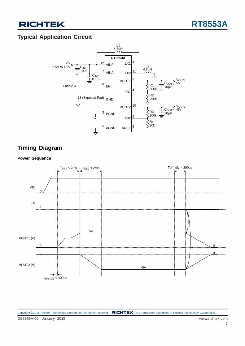
Typical Application Circuit
Timing Diagram
Power Sequence
VIN
VOUT1 (V)
VOUT2 (V)
0
0
5V
0
0
-5V
TSS1 < 2ms
0
0
TSS2 < 2ms Toff_dly > 300us
tEN_Dly < 400us
EN
VINP LX1
VOUT2
VIN
PGND
RT8553A
10µF
12 1
10
3
2.5V to 4.5V CIN1
L14.7µH
VINA7
EN6
VOUT1 2
10µFCOUT1
VOUT15V
LX2 11
L24.7µH
AGND5
Enable800kR1
200kR2
10µFCOUT2
VOUT2-5V
100kR3
20kR4
FB1 4
FB2 9
VREF 8
GND13 (Exposed Pad)
0.1µFCIN2
RT8553A
8
DS8553A-00 January 2015www.richtek.com
©Copyright 2015 Richtek Technology Corporation. All rights reserved. is a registered trademark of Richtek Technology Corporation.
VOUT2 vs. Input Voltage
-5.020
-5.015
-5.010
-5.005
-5.000
-4.995
-4.990
-4.985
2.9 3.1 3.3 3.5 3.7 3.9 4.1 4.3 4.5
Input Voltage (V)
VO
UT
2 (V
)
VOUT1 vs. Input Voltage
4.970
4.975
4.980
4.985
4.990
4.995
5.000
5.005
2.9 3.1 3.3 3.5 3.7 3.9 4.1 4.3 4.5
Input Voltage (V)
VO
UT
1 (V
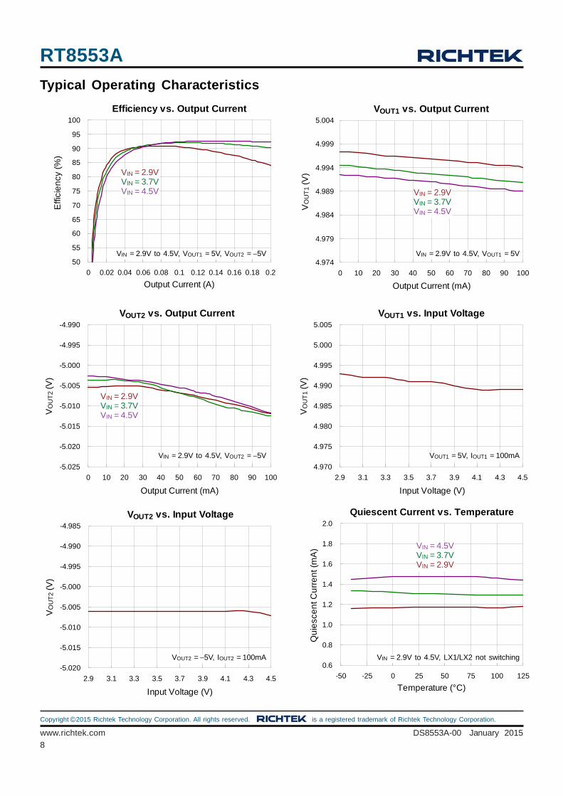
)VOUT2 vs. Output Current
-5.025
-5.020
-5.015
-5.010
-5.005
-5.000
-4.995
-4.990
0 10 20 30 40 50 60 70 80 90 100
Output Current (mA)
VO
UT
2 (V
)
VOUT1 vs. Output Current
4.974
4.979
4.984
4.989
4.994
4.999
5.004
0 10 20 30 40 50 60 70 80 90 100
Output Current (mA)
VO
UT
1 (V
)
VIN = 2.9VVIN = 3.7VVIN = 4.5V
VIN = 2.9V to 4.5V, VOUT1 =
5V
VOUT2 = −5V, IOUT2 =
100mA
Quiescent Current vs. Temperature
0.6
0.8
1.0
1.2
1.4
1.6
1.8
2.0
-50 -25 0 25 50 75 100 125
Temperature (°C)
Qu
iesc
en
t Cu
rre
nt (
mA
)
VIN = 2.9V to 4.5V, LX1/LX2 not switching
VIN = 4.5VVIN = 3.7VVIN = 2.9V
VOUT1 = 5V, IOUT1 =
100mA
VIN = 2.9VVIN = 3.7VVIN = 4.5V
VIN = 2.9V to 4.5V, VOUT2 =
−5V
Efficiency vs. Output Current
50
55
60
65
70
75
80
85
90
95
100
0 0.02 0.04 0.06 0.08 0.1 0.12 0.14 0.16 0.18 0.2
Output Current (A)
Effi
cie
ncy
(%
)
VIN = 2.9VVIN = 3.7VVIN = 4.5V
VIN = 2.9V to 4.5V, VOUT1 =
5V, VOUT2 =
−5V
Typical Operating Characteristics
RT8553A
9
DS8553A-00 January 2015 www.richtek.com
©Copyright 2015 Richtek Technology Corporation. All rights reserved. is a registered trademark of Richtek Technology Corporation.
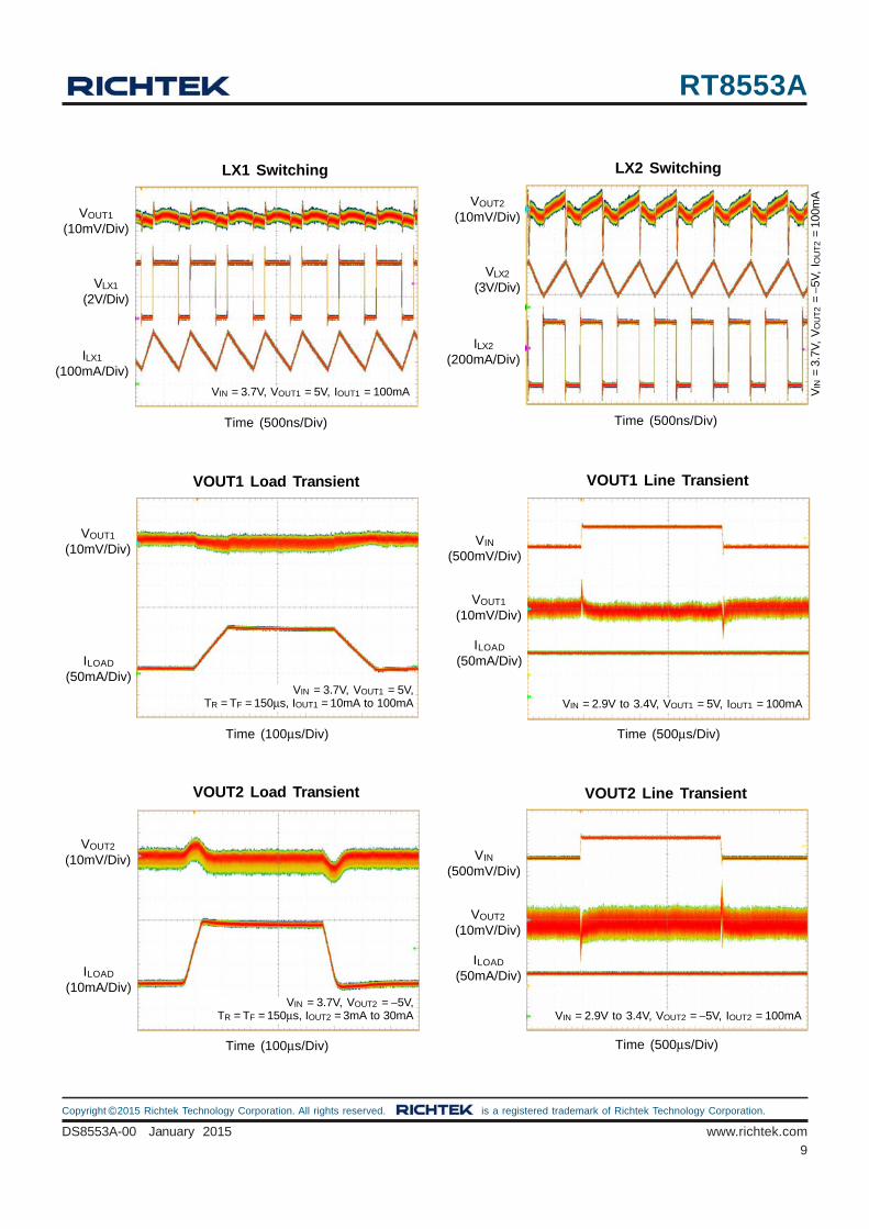
Time (500ns/Div)
LX2 Switching
VIN
= 3
.7V
, V
OU
T2
= −
5V,
I OU
T2
= 1
00m
AVOUT2
(10mV/Div)
VLX2
(3V/Div)
ILX2
(200mA/Div)
Time (500ns/Div)
LX1 Switching
VOUT1
(10mV/Div)
VLX1
(2V/Div)
ILX1
(100mA/Div)
VIN = 3.7V, VOUT1 =
5V, IOUT1 =
100mA
Time (100μs/Div)
VOUT1 Load Transient
VOUT1
(10mV/Div)
ILOAD
(50mA/Div)VIN =
3.7V, VOUT1 =
5V,
TR = TF =
150μs, IOUT1 =
10mA to 100mA
Time (500μs/Div)
VOUT1 Line Transient
VOUT1
(10mV/Div)
ILOAD
(50mA/Div)
VIN
(500mV/Div)
VIN = 2.9V to 3.4V, VOUT1 =
5V, IOUT1 =
100mA
Time (100μs/Div)
VOUT2 Load Transient
VOUT2
(10mV/Div)
ILOAD
(10mA/Div)VIN =
3.7V, VOUT2 =
−5V,
TR = TF =
150μs, IOUT2 =
3mA to 30mA VIN =
2.9V to 3.4V, VOUT2 =
−5V, IOUT2 =
100mA
Time (500μs/Div)
VOUT2 Line Transient
VOUT2
(10mV/Div)
ILOAD
(50mA/Div)
VIN
(500mV/Div)
RT8553A
10
DS8553A-00 January 2015www.richtek.com
©Copyright 2015 Richtek Technology Corporation. All rights reserved. is a registered trademark of Richtek Technology Corporation.
VIN = 3.7V, VOUT1 =
5V,
VOUT2 = −5V, No Load
Time (2ms/Div)
Power On Sequence
EN(2V/Div)
VOUT1
(2V/Div)VOUT2
(2V/Div)
IIN
(200mA/Div)
Time (2ms/Div)
Power Off Sequence
EN(2V/Div)
VOUT1
(2V/Div)
VOUT2
(2V/Div)
IIN
(200mA/Div)
VIN = 3.7V, VOUT1 =
5V,
VOUT2 = −5V, No Load
RT8553A
11
DS8553A-00 January 2015 www.richtek.com
©Copyright 2015 Richtek Technology Corporation. All rights reserved. is a registered trademark of Richtek Technology Corporation.
Application Information
The RT8553A is a dual channel DC/DC converter capable
of generating both positive and negative outputs by external
feedback voltage-divider resistors from an input voltage
range of 2.5V to 4.5V. Each converter works independently
of one another and both outputs are separately controlled
by a fixed frequency Pulse-Width-Modulated (PWM)
regulator.
Soft-Start
The RT8553A employs a soft-start feature for both
converters to limit the inrush current and prevent input
voltage droop. When each converter is enabled, the
implemented switch current limit ramps up slowly to its
nominal programmed value in about 2ms for the Boost
converter and Buck-Boost converter.
Over-Voltage Protection (OVP)
The RT8553A has over-voltage circuit protection
mechanism which prevents feedback pin floating when the
IC is enabled. When output voltage exceeds OVP
threshold voltage, the IC would be clamped at fixed voltage
with minimum duty.
Over-Current Protection (OCP)
The RT8553A includes a current sensing circuitry which
monitors the inductor current during each charging cycle.
If the current value becomes greater than the current limit,
the converter will be shutdown and can only re-start normal
operation after triggering EN pin or re-power on again.
Over-Temperature Protection (OTP)
The RT8553A includes an Over-Temperature Protection
(OTP) feature to prevent the device from overheat due to
excessive power dissipation. The OTP function shuts down
all device operations when the junction temperature
exceeds 140°C. Once the junction temperature cools
down by approximately 15°C, the converter resumes
operation. To maintain continuous operation, prevent the
maximum junction temperature form rising above 125°C.
Under-Voltage Lockout (UVLO)
The Under-Voltage Lockout (UVLO) circuitry compares
the input voltage with the UVLO threshold to ensure that
the input voltage is high enough for reliable operation.
Once the input voltage exceeds the UVLO rising threshold
at 2.22V (typ.), start-up begins. A 40mV (typ.) hysteresis
is included to prevent supply transients from causing a
shutdown.
Positive Output Voltage Setting
The output voltage setting can be calculated according to
the following equation :
OUT OUT(MAX)IN(MAX)
IN
L IN(MAX)
V II =
V
I = 0.4 I
where VFB1 is the reference voltage with a typical value of
1V.
Input Capacitor Selection
Input ceramic capacitors with 10μF capacitance are
suggested for the RT8553A applications. However, to
achieve best performance with the RT8553A, larger
capacitance can be used. For better voltage filtering, select
ceramic capacitors with low ESR, X5R and X7R types are
suitable because of their wider voltage and temperature
ranges.
Boost Inductor Selection
The inductance depends on the maximum input current.
As a general rule, the inductor ripple current range is 20%
to 40% of the maximum input current. If 40% is selected
as an example, the inductor ripple current can be
calculated according to the following equations :
where η is the efficiency of the converter, IIN(MAX) is the
maximum input current, and ΔIL is the inductor ripple
current. The input peak current can then be obtained by
adding the maximum input current with half of the inductor
ripple current as shown in the following equation :
Ipeak = 1.2 x IIN(MAX)
OUT1 FB1R1V = V 1R2
RT8553A
12
DS8553A-00 January 2015www.richtek.com
©Copyright 2015 Richtek Technology Corporation. All rights reserved. is a registered trademark of Richtek Technology Corporation.
IN L OUT IN L OUT
INOUT OUT1
OUT OSC
1 1 1Q = I + I I + I I I2 2 2
V 1 = C VV f
OUT2 FB2 REF FB2R3V = V V VR4
Note that the saturated current of the inductor must be
greater than Ipeak.
The inductance can eventually be determined according
to the following equation :
2IN OUT IN
2OUT OUT(MAX) OSC
V (V V )L =
0.4 V I f
where fOSC is the switching frequency. For better system
performance, a shielded inductor is preferred to avoid EMI
problems.
Boost Output Capacitor Selection
The output ripple voltage is an important index for
estimating chip performance. This portion consists of two
parts. One is the product of the inductor peak current
with the ESR of the output capacitor, while the other part
is formed by the charging and discharging process of the
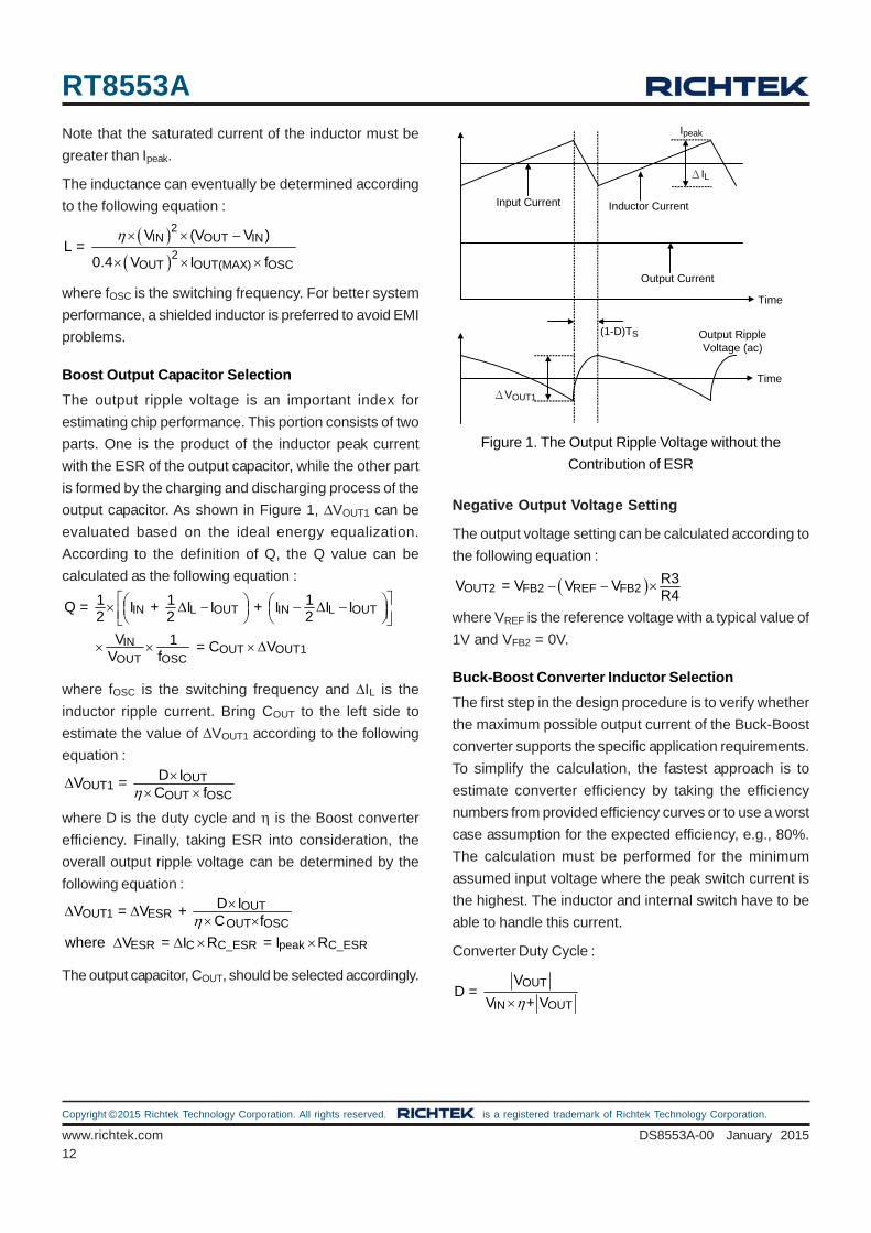
output capacitor. As shown in Figure 1, ΔVOUT1 can be
evaluated based on the ideal energy equalization.
According to the definition of Q, the Q value can be
calculated as the following equation :
OUTOUT1
OUT OSC
D IV = C f
OUTOUT1 ESR
OUT OSC
ESR C C_ESR peak C_ESR
D IV = V + C f
where V = I R = I R
where fOSC is the switching frequency and ΔIL is the
inductor ripple current. Bring COUT to the left side to
estimate the value of ΔVOUT1 according to the following
equation :
where D is the duty cycle and η is the Boost converter
efficiency. Finally, taking ESR into consideration, the
overall output ripple voltage can be determined by the
following equation :
The output capacitor, COUT, should be selected accordingly.
Time
Time
Inductor Current
Output Current
Output Ripple Voltage (ac)
(1-D)TS
ΔVOUT1
ΔIL
Input Current
Ipeak
Figure 1. The Output Ripple Voltage without the
Contribution of ESR
Negative Output Voltage Setting
The output voltage setting can be calculated according to
the following equation :
where VREF is the reference voltage with a typical value of
1V and VFB2 = 0V.
Buck-Boost Converter Inductor Selection
The first step in the design procedure is to verify whether
the maximum possible output current of the Buck-Boost
converter supports the specific application requirements.
To simplify the calculation, the fastest approach is to
estimate converter efficiency by taking the efficiency
numbers from provided efficiency curves or to use a worst
case assumption for the expected efficiency, e.g., 80%.
The calculation must be performed for the minimum
assumed input voltage where the peak switch current is
the highest. The inductor and internal switch have to be
able to handle this current.
Converter Duty Cycle :
OUT
IN OUT
VD =
V + V
RT8553A
13
DS8553A-00 January 2015 www.richtek.com
©Copyright 2015 Richtek Technology Corporation. All rights reserved. is a registered trademark of Richtek Technology Corporation.
0.0
0.5
1.0
1.5
2.0
2.5
3.0
3.5
0 25 50 75 100 125
Ambient Temperature (°C)
Ma
xim
um
Po
we
r D
issi
pa
tion
(W
) 1
OUTESR
OSC LOAD OUT
ESR C C_ESR peak C_ESR
D VV = + V
f R Cwhere V = I R = I R
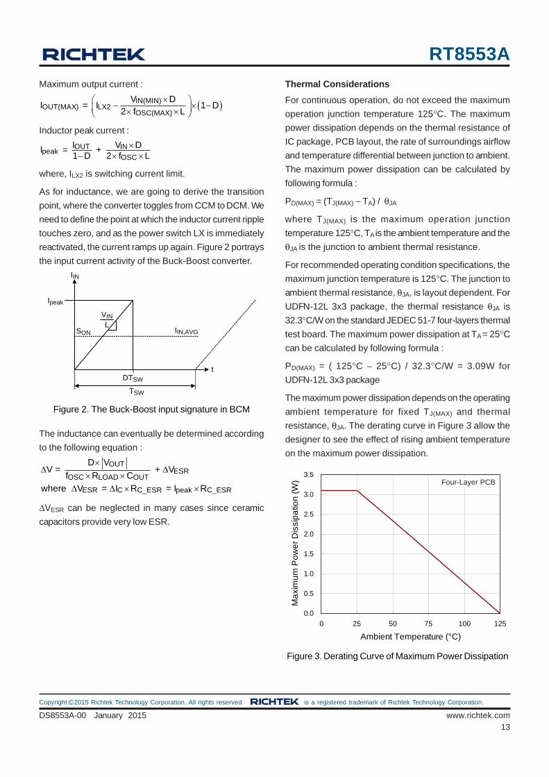
Figure 2. The Buck-Boost input signature in BCM
IIN
Ipeak
SON IIN,AVG
DTSW
TSW
t
VIN
L
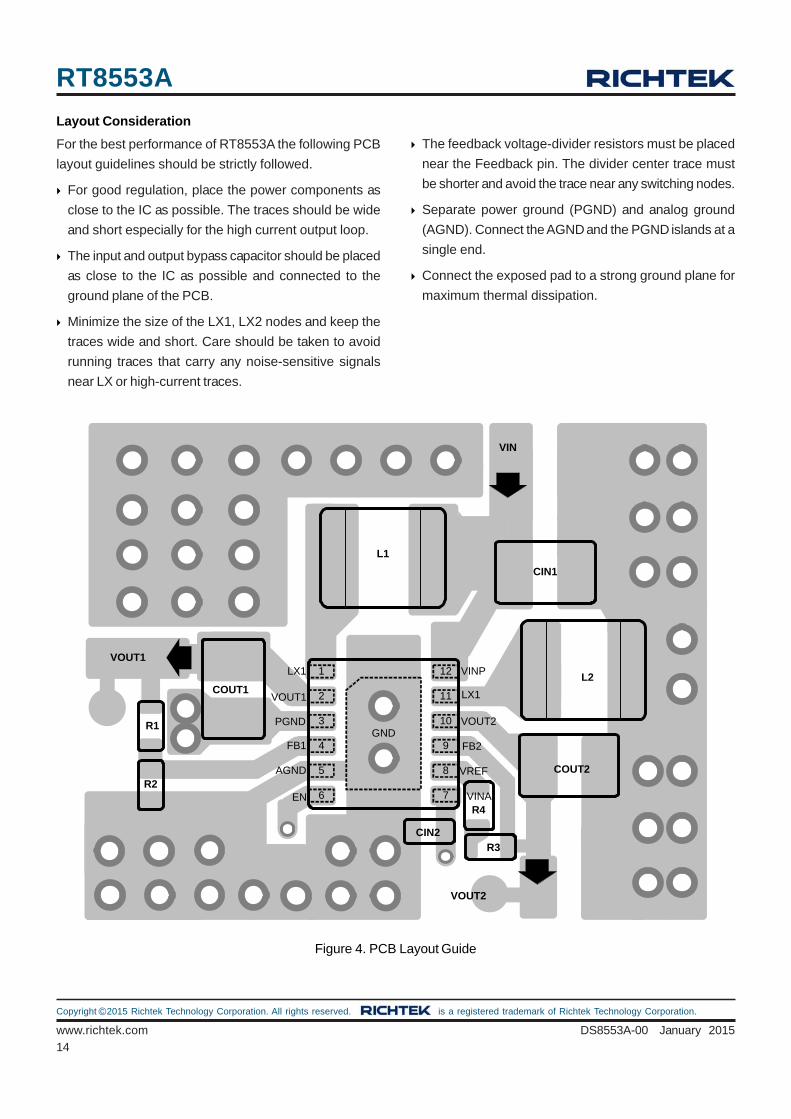
Thermal Considerations
For continuous operation, do not exceed the maximum
operation junction temperature 125°C. The maximum
power dissipation depends on the thermal resistance of
IC package, PCB layout, the rate of surroundings airflow
and temperature differential between junction to ambient.
The maximum power dissipation can be calculated by
following formula :
PD(MAX) = (TJ(MAX) − TA) / θJA
where TJ(MAX) is the maximum operation junction
temperature 125°C, TA is the ambient temperature and the
θJA is the junction to ambient thermal resistance.
For recommended operating condition specifications, the
maximum junction temperature is 125°C. The junction to
ambient thermal resistance, θJA, is layout dependent. For
UDFN-12L 3x3 package, the thermal resistance θJA is
32.3°C/W on the standard JEDEC 51-7 four-layers thermal
test board. The maximum power dissipation at TA = 25°Ccan be calculated by following formula :
PD(MAX) = ( 125°C − 25°C) / 32.3°C/W = 3.09W for
UDFN-12L 3x3 package
The maximum power dissipation depends on the operating
ambient temperature for fixed TJ(MAX) and thermal
resistance, θJA. The derating curve in Figure 3 allow the
designer to see the effect of rising ambient temperature
on the maximum power dissipation.
Figure 3. Derating Curve of Maximum Power Dissipation
Four-Layer PCB
IN(MIN)OUT(MAX) LX2
OSC(MAX)
V DI = I 1 D
2 f L
OUT INpeak
OSC
I V DI = + 1 D 2 f L
Maximum output current :
Inductor peak current :
where, ILX2 is switching current limit.
As for inductance, we are going to derive the transition
point, where the converter toggles from CCM to DCM. We
need to define the point at which the inductor current ripple
touches zero, and as the power switch LX is immediately
reactivated, the current ramps up again. Figure 2 portrays
the input current activity of the Buck-Boost converter.
The inductance can eventually be determined according
to the following equation :
ΔVESR can be neglected in many cases since ceramic
capacitors provide very low ESR.
©Copyright 2015 Richtek Technology Corporation. All rights reserved. is a registered trademark of Richtek Technology Corporation.
RT8553A
14
DS8553A-00 January 2015www.richtek.com
Layout Consideration
For the best performance of RT8553A the following PCB
layout guidelines should be strictly followed.
For good regulation, place the power components as
close to the IC as possible. The traces should be wide
and short especially for the high current output loop.
The input and output bypass capacitor should be placed
as close to the IC as possible and connected to the
ground plane of the PCB.
Minimize the size of the LX1, LX2 nodes and keep the
traces wide and short. Care should be taken to avoid
running traces that carry any noise-sensitive signals
near LX or high-current traces.
The feedback voltage-divider resistors must be placed
near the Feedback pin. The divider center trace must
be shorter and avoid the trace near any switching nodes.
Separate power ground (PGND) and analog ground
(AGND). Connect the AGND and the PGND islands at a
single end.
Connect the exposed pad to a strong ground plane for
maximum thermal dissipation.
Figure 4. PCB Layout Guide
L2
CIN1
COUT2
COUT1
VIN
VOUT1
VOUT2
LX1
PGND
VOUT1
FB1
AGND VREF
1
2
3
4
5
6
10
9
8
7
11
12 VINP
LX1
VOUT2
FB2
EN
GND
VINA
L1
R2
R1
R4
R3
CIN2
RT8553A
15
DS8553A-00 January 2015 www.richtek.com
Richtek Technology Corporation14F, No. 8, Tai Yuen 1st Street, Chupei City
Hsinchu, Taiwan, R.O.C.
Tel: (8863)5526789
Richtek products are sold by description only. Richtek reserves the right to change the circuitry and/or specifications without notice at any time. Customers should
obtain the latest relevant information and data sheets before placing orders and should verify that such information is current and complete. Richtek cannot
assume responsibility for use of any circuitry other than circuitry entirely embodied in a Richtek product. Information furnished by Richtek is believed to be
accurate and reliable. However, no responsibility is assumed by Richtek or its subsidiaries for its use; nor for any infringements of patents or other rights of third
parties which may result from its use. No license is granted by implication or otherwise under any patent or patent rights of Richtek or its subsidiaries.
Outline Dimension
U-Type 12L DFN 3x3 Package
1 122
Note : The configuration of the Pin #1 identifier is optional,
but must be located within the zone indicated.
DETAIL A
Pin #1 ID and Tie Bar Mark Options
Min. Max. Min. Max.
A 0.500 0.600 0.020 0.024
A1 0.000 0.050 0.000 0.002
A3 0.100 0.175 0.004 0.007
b 0.150 0.250 0.006 0.010
D 2.950 3.050 0.116 0.120
D2 2.300 2.650 0.091 0.104
E 2.950 3.050 0.116 0.120
E2 1.400 1.750 0.055 0.069
e
L 0.350 0.450 0.014 0.018
SymbolDimensions In Millimeters Dimensions In Inches
0.450 0.018
Related Documents