OPTICAL METAMATERIALS: DESIGN, CHARACTERIZATION AND APPLICATIONS BY PRATIK CHATURVEDI B.Tech., Indian Institute of Technology Bombay, 2004 M.S., University of Illinois at Urbana-Champaign, 2006 DISSERTATION Submitted in partial fulfillment of the requirements for the degree of Doctor of Philosophy in Mechanical Engineering in the Graduate College of the University of Illinois at Urbana-Champaign, 2009 Urbana, Illinois Doctoral Committee: Assistant Professor Nicholas X. Fang, Chair Associate Professor Paul Scott Carney Associate Professor Harley T. Johnson Assistant Professor Xiuling Li

Welcome message from author
This document is posted to help you gain knowledge. Please leave a comment to let me know what you think about it! Share it to your friends and learn new things together.
Transcript
OPTICAL METAMATERIALS: DESIGN, CHARACTERIZATION AND APPLICATIONS
BY
PRATIK CHATURVEDI
B.Tech., Indian Institute of Technology Bombay, 2004 M.S., University of Illinois at Urbana-Champaign, 2006
DISSERTATION
Submitted in partial fulfillment of the requirements for the degree of Doctor of Philosophy in Mechanical Engineering
in the Graduate College of the University of Illinois at Urbana-Champaign, 2009
Urbana, Illinois
Doctoral Committee: Assistant Professor Nicholas X. Fang, Chair Associate Professor Paul Scott Carney
Associate Professor Harley T. Johnson Assistant Professor Xiuling Li
ii
ABSTRACT
Artificially engineered metamaterials have emerged with properties and
functionalities previously unattainable in natural materials. The scientific breakthroughs
made in this new class of electromagnetic materials are closely linked with progress in
developing physics-driven design, novel fabrication and characterization methods. The
intricate behavior of these novel metamaterials is interesting from both fundamental and
practical point of view. New frontiers are being explored as intrinsic limitations challenge
the scaling of microwave metamaterial designs to optical frequencies. These materials
promise an entire new generation of miniaturized passive and active optical elements. In
this study, I demonstrate an on-fiber integrated “fishnet” metamaterial modulator for
telecommunication applications. This metamaterial shows remarkable coupling to fiber
guided modes (3.5dB) and a photoswitchable tuning range of more than 1.8dB. The
design offers extremely small footprint (~10 wavelengths) and complete elimination of
bulk optical components to realize low-cost, potential high-speed optical switching and
modulation.
Unique characterization techniques need to be developed as conventional optical
microscopy runs out of steam to resolve the fine features of optical metamaterials. To
address this challenge, I have investigated cathodoluminescence imaging and
spectroscopy technique. This scanning electron beam based technique allows optical
image acquisition and spectroscopy with high spectral and spatial resolution.
Monochromatic photon maps (spectral bandwidth ~5nm) show strong variation of
localized plasmon modes on length scales as small as 25nm. Numerical simulations
performed to model the eigenmodes excited by electron beam show strong agreement
with experiments.
I also demonstrate progress made in “superlensing”, a phenomenon associated
with plasmonic metamaterials, leading to subdiffraction resolution with optical imaging.
Fabricating a smooth silver superlens (0.6nm root mean square roughness) with 15nm
thickness, I demonstrate 30nm imaging resolution or 1/12th of the illumination
wavelength (near-ultraviolet), far below the diffraction-limit. Moreover, I have extended
subdiffraction imaging to far-field at infrared wavelengths. Utilizing a two-dimensional

iii
array of silver nanorods that provides near-field enhancement, I numerically show that
subwavelength features can be resolved in far-field in the form of Moiré features.
Development of this unique far-field superlensing phenomenon at infrared wavelengths is
of significant importance to chemical and biomedical imaging.

iv
In memory of Dada and Jee
v
ACKNOWLEDGEMENTS
I have been fortunate to be surrounded by many loving people and it is my great
pleasure to thank them for their love, support, blessings and encouragement.
First of all, I would like to express my sincere gratitude towards my advisor Prof.
Nicholas Fang, for his unending support and valuable guidance throughout the course of
my graduate studies. His confidence in my abilities was crucial to smooth my transition
from traditional engineering background into the realm of nanotechnology. Without his
exemplary vision, optimism and encouragement, this work could not have taken its
present shape.
During the course of my graduate studies, I had the opportunity to work with a
number of collaborators. I am thankful to Keng Hsu and Anil Kumar for help with
fabricating various samples; Hyungjin Ma, and Xu Jun for optical characterization; Kin
Hung Fung and Lumerical technical support group for various stimulating discussions on
numerical simulations. Special thanks to Dr. James Mabon for help with carrying out
cathodoluminescence measurements. I also had the pleasure to work with researchers and
collaborators from HP Labs. Dr. Wei Wu, Dr. S. Y. Wang, VJ Logeeswaran provided
timely help and support. I am thankful to all other lab members Chunguang Xia, Tarun
Malik, Shu Zhang, Ho Won Lee, and Matthew Alonso for providing a friendly work
environment. I am grateful to my committee members Prof. Paul Scott Carney, Prof.
Harley Johnson, and Prof. Xiuling Li for their valuable time and suggestions.
I am thankful to all my friends who kept me company and made me feel at home
in Urbana-Champaign. My parents, my sister, brother and relatives have been a constant
source of unconditional love and support all throughout my life. Expressing my gratitude
in words towards them is an exercise in futility. Nikki came into my life during the final
stages of my PhD; she helped me get past my worries and stood by me during this long
process.
Finally I would like to thank all the funding resources DARPA, NSF, and DoE for
supporting my research work at University of Illinois.

vi
TABLE OF CONTENTS
1 INTRODUCTION..................................................................................................... 1
1.1 Background and motivation................................................................................ 1
1.2 Thesis organization ............................................................................................. 7
2 INTEGRATED METAMATERIAL MODULATOR ON OPTICAL FIBER ... 9
2.1 Introduction......................................................................................................... 9
2.2 Free-space fishnet metamaterial modulator ...................................................... 11
2.3 Integrated fishnet metamaterial modulator ....................................................... 16
2.4 Towards improving modulator performance .................................................... 25
2.5 Summary ........................................................................................................... 33
3 IMAGING OF PLASMONIC MODES OF NANOSTRUCTURES USING
HIGH-RESOLUTION CATHODOLUMINESCENE SPECTROSCOPY............... 34
3.1 Introduction....................................................................................................... 34
3.2 Results and discussion ...................................................................................... 37
3.3 Summary ........................................................................................................... 50
4 SUBDIFFRACTION SUPERLENS IMAGING WITH PLASMONIC
METAMATERIALS ...................................................................................................... 53
4.1 Introduction....................................................................................................... 53
4.2 Smooth superlens .............................................................................................. 54
4.3 Subdiffraction far-field imaging in infrared ..................................................... 61
4.4 Summary ........................................................................................................... 74
5 SUMMARY, FUTURE WORK AND OUTLOOK ............................................. 77
5.1 Summary ........................................................................................................... 77
5.2 Future work....................................................................................................... 78
5.3 Outlook ............................................................................................................. 78
REFERENCES................................................................................................................ 80
AUTHOR’S BIOGRAPHY............................................................................................ 88
1
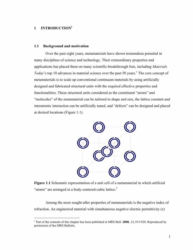
1 INTRODUCTION∗
1.1 Background and motivation
Over the past eight years, metamaterials have shown tremendous potential in
many disciplines of science and technology. Their extraordinary properties and
applications has placed them on many scientific-breakthrough lists, including Materials
Today’s top 10 advances in material science over the past 50 years.1 The core concept of
metamaterials is to scale up conventional continuum materials by using artificially
designed and fabricated structural units with the required effective properties and
functionalities. These structural units considered as the constituent “atoms” and
“molecules” of the metamaterial can be tailored in shape and size, the lattice constant and
interatomic interaction can be artificially tuned, and “defects” can be designed and placed
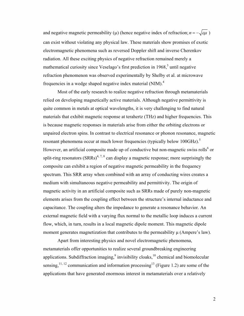
at desired locations (Figure 1.1).
Figure 1.1 Schematic representation of a unit cell of a metamaterial in which artificial
“atoms” are arranged in a body-centered-cubic lattice.2
Among the most sought-after properties of metamaterials is the negative index of
refraction. An engineered material with simultaneous negative electric permittivity (ε)
∗ Part of the contents of this chapter has been published in MRS Bull. 2008, 33, 915-920. Reproduced by permission of the MRS Bulletin.
2
and negative magnetic permeability (µ) (hence negative index of refraction; n εμ= − )
can exist without violating any physical law. These materials show promises of exotic
electromagnetic phenomena such as reversed Doppler shift and inverse Cherenkov
radiation. All these exciting physics of negative refraction remained merely a
mathematical curiosity since Veselago’s first prediction in 1968,3 until negative
refraction phenomenon was observed experimentally by Shelby et al. at microwave
frequencies in a wedge shaped negative index material (NIM).4
Most of the early research to realize negative refraction through metamaterials
relied on developing magnetically active materials. Although negative permittivity is
quite common in metals at optical wavelengths, it is very challenging to find natural
materials that exhibit magnetic response at terahertz (THz) and higher frequencies. This
is because magnetic responses in materials arise from either the orbiting electrons or
unpaired electron spins. In contrast to electrical resonance or phonon resonance, magnetic
resonant phenomena occur at much lower frequencies (typically below 100GHz).5
However, an artificial composite made up of conductive but non-magnetic swiss rolls6 or
split-ring resonators (SRRs)4, 7, 8 can display a magnetic response; more surprisingly the
composite can exhibit a region of negative magnetic permeability in the frequency
spectrum. This SRR array when combined with an array of conducting wires creates a
medium with simultaneous negative permeability and permittivity. The origin of
magnetic activity in an artificial composite such as SRRs made of purely non-magnetic
elements arises from the coupling effect between the structure’s internal inductance and
capacitance. The coupling alters the impedance to generate a resonance behavior. An
external magnetic field with a varying flux normal to the metallic loop induces a current
flow, which, in turn, results in a local magnetic dipole moment. This magnetic dipole
moment generates magnetization that contributes to the permeability μ (Ampere’s law).
Apart from interesting physics and novel electromagnetic phenomena,
metamaterials offer opportunities to realize several groundbreaking engineering
applications. Subdiffraction imaging,9 invisibility cloaks,10 chemical and biomolecular
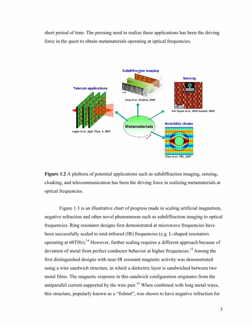
sensing,11, 12 communication and information processing13 (Figure 1.2) are some of the
applications that have generated enormous interest in metamaterials over a relatively
3
short period of time. The pressing need to realize these applications has been the driving
force in the quest to obtain metamaterials operating at optical frequencies.
Figure 1.2 A plethora of potential applications such as subdiffraction imaging, sensing,
cloaking, and telecommunication has been the driving force in realizing metamaterials at
optical frequencies.
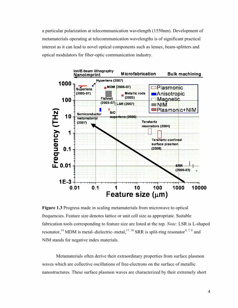
Figure 1.3 is an illustrative chart of progress made in scaling artificial magnetism,
negative refraction and other novel phenomenon such as subdiffraction imaging to optical
frequencies. Ring resonator designs first demonstrated at microwave frequencies have
been successfully scaled to mid-infrared (IR) frequencies (e.g. L-shaped resonators
operating at 60THz).14 However, further scaling requires a different approach because of
deviation of metal from perfect conductor behavior at higher frequencies.15 Among the
first distinguished designs with near-IR resonant magnetic activity was demonstrated
using a wire sandwich structure, in which a dielectric layer is sandwiched between two
metal films. The magnetic response in this sandwich configuration originates from the
antiparallel current supported by the wire pair.16 When combined with long metal wires,
this structure, popularly known as a “fishnet”, was shown to have negative refraction for
4
a particular polarization at telecommunication wavelength (1550nm). Development of
metamaterials operating at telecommunication wavelengths is of significant practical
interest as it can lead to novel optical components such as lenses, beam-splitters and
optical modulators for fiber-optic communication industry.
Figure 1.3 Progress made in scaling metamaterials from microwave to optical
frequencies. Feature size denotes lattice or unit cell size as appropriate. Suitable
fabrication tools corresponding to feature size are listed at the top. Note: LSR is L-shaped
resonator,14 MDM is metal–dielectric–metal,17, 18 SRR is split-ring resonator4, 7, 8 and
NIM stands for negative index materials.
Metamaterials often derive their extraordinary properties from surface plasmon
waves which are collective oscillations of free-electrons on the surface of metallic
nanostructures. These surface plasmon waves are characterized by their extremely short
5
wavelength and thus provide a natural interface to couple light to much smaller nanoscale
devices more effectively. An entire new generation of metamaterials termed as plasmonic
metamaterials operates simply by harnessing properties of resonant surface plasmons.
Amplification of evanescent waves,19 achievement of negative refractive index such as in
fishnet metamaterial,20 extraordinary transmission enhancement,21 and enhanced Raman
scattering22 are some of the surface plasmons driven phenomena that offer great
opportunities for several applications. Optical imaging with subdiffraction resolution,
nanolithography, and detection of chemical and biological species with single molecule
sensitivity represent some of the possibilities. For example, a planar silver (Ag) film
(termed as superlens) is one of the simplest forms of plasmonic metamaterials with an
extraordinary ability to beat the diffraction limit through amplification of evanescent
waves.19 Artificial plasmonic metamaterials also offer an opportunity to engineer surface
modes over a wide range of frequency by simple surface patterning. Patterning also
allows strong confinement and enhancement of resonant plasmon modes compared to flat
metal films.23 These metallic patterns are often utilized in surface-enhanced Raman
spectroscopy (SERS) as sensing substrates.
The intricate structure of these novel metamaterials and devices is derived from
physics-driven design for desired properties and applications. These designs require
development of viable manufacturing and novel characterization techniques. In this
dissertation, I have explored the field of optical metamaterials to address three of the
most important applications in optical regime, namely telecommunication, optical
imaging beyond diffraction limit and chemical sensing. With an exceptional team of
experts in the field of plasmonic metamaterials, we set to explore these applications with
an integrated approach; starting with fundamental understanding of the physics of
metamaterials to developing simulation, fabrication and characterization tools in order to
build a continuum picture. The objective of this research is three fold: (1) to develop an
integrated metamaterial modulator on an optical fiber for telecommunication
applications, (2) to explore cathodoluminescence (CL) spectroscopy as a characterization
technique for imaging of plasmonic modes of metallic nanostructures, and (3) to refine
the subdiffraction imaging capability of silver superlenses operating in near-ultraviolet
6
(UV) and develop novel far-field superlenses for near and mid-infrared (IR) frequencies
for chemical sensing applications.
The first objective is inspired by an inevitable thrust of research and development
in photonics to drive to ever higher levels of integration, eventually leading to a “Moore’s
Law” for optical information technology, requiring the exponential growth of information
processing functions such as modulating and switching at small scales. A significant
roadblock towards that goal is the size and cost of discrete optical components. In this
research, we explore novel concepts of metamaterials to address these ultimate demands.
We have investigated the fishnet metamaterial design and its possible integration on to an
optical fiber to develop a lightweight, compact and efficient telecommunication
modulator.
The second objective sets to explore the properties of plasmonic metamaterials
using CL imaging and spectroscopy. This part of the research addresses the pressing need
to develop unique characterization techniques for the analysis of subwavelength and
complex metastructures. Existing characterization methods ranging from optical
microscopy to near-field scanning optical microscopy (NSOM) do not offer the flexibility
of characterizing optical metamaterials with features on the order of sub-10s of
nanometers. On the other hand CL, a scanning electron beam based characterization
technique offers an opportunity to investigate these structures with unprecedented
resolution. This investigation is critical to fully understand and exploit the properties of
metal nanostructures.
The third objective deals with one of the most promising applications of
metamaterials; their ability to obtain images that are diffraction free. Inspired by recent
work on superlens imaging9 we set to explore the ultimate limit of subdiffraction imaging
with silver superlenses. While these superlenses are limited to providing subdiffraction
images only in the near-field, we have explored an imaging approach based on Moiré
effect that allows subdiffraction resolution in the far-field at IR frequency range. This
frequency range is of special interest to chemists and biologists who utilize IR imaging
tools such as Fourier-transform infrared imaging (FT-IR) and spectroscopy to detect trace
amounts of chemicals and malignancy in biological cells and tissues. The development of
7
a parallel far-field optical imaging tool with subdiffraction resolution could have a
profound impact in chemical sensing and medical diagnostics.
1.2 Thesis organization
This dissertation is organized into 5 chapters. Besides this introductory chapter
which is intended to provide a brief background and outline of the study, the contents of
rest of the chapters are organized as follows.
Chapter 2 discusses the development of “Integrated metamaterial modulator on
optical fiber” for telecommunication. We have investigated the fishnet metamaterial as an
optical modulator for on-fiber communication and information processing applications.
The design offers small footprint (~10-20λ, where λ is free-space wavelength) and
integration on fiber eliminates the need for bulk optical components. Numerical studies
indicate 3.5dB in transmission dip due to coupling of fiber guided modes with that of the
metamaterial and an on/off ratio of 1.8dB for the integrated modulator. We have also
investigated a “flipped fishnet” geometry that shows low loss and stronger coupling with
fiber-guided modes.
Chapter 3 presents “Imaging of plasmonic modes of nanostructures using high-
resolution cathodoluminescence spectroscopy”. Most of the prevalent optical
metamaterial designs are based on nanostructures made of noble metals such as silver and
gold. To investigate the optical properties of such structures, we have performed CL
spectroscopy on silver nanoparticles in a scanning electron microscopy setup. Direct
excitation and emission of decoupled surface plasmon modes is observed with
panchromatic and monochromatic imaging techniques. Monochromatic emission maps
have been shown to resolve spatial field variation of resonant plasmon mode on length
scale smaller than 25nm. Finite-difference time-domain numerical simulations are
performed for both the cases of light excitation and electron excitation. The results of
radiative emission under electron excitation show an excellent agreement with
experiments. A complete vectorial description of induced field is given, which
complements the information obtained from experiments.
8
Since its conceptualization24 superlens has received great deal of attention from
the scientific community owing to its superior imaging capabilities with subdiffraction
resolution. Theoretically, the device is capable of λ/20 - λ/30 image resolution25, 26.
However, after the first demonstration of λ/6 imaging (60nm resolution)with a silver
superlens,9 no further improvement in resolution has been reported so far, mainly because
it requires fabrication of thin, ultra-smooth silver film, which presents a daunting
challenge owing to island forming tendencies of silver.27 In Chapter 4, we show a smooth
superlens (~0.6nm root mean square roughness) can be fabricated down to 15nm
thickness. Utilizing an intermediate wetting layer germanium for the growth of silver, we
experimentally demonstrate 30nm or λ/12 optical imaging resolution at near-UV
wavelength. Moreover, we have conceived a novel far-field subdiffraction imaging
scheme at IR wavelengths. Utilizing a plasmonic material consisting of array of silver
nanorods, we numerically demonstrate that subwavelength information from an object
can be coupled out to the far-field in the form of Moiré features. A simple image
reconstruction algorithm can then be applied to recover the object with subwavelength
resolution. Realization of such a far-field superlens opens up exciting avenues for
biomedical imaging and chemical analysis.
Finally, Chapter 5 provides the summary of the work presented in this dissertation
and gives an outlook on possible future directions.
9
2 INTEGRATED METAMATERIAL MODULATOR ON OPTICAL FIBER
2.1 Introduction
In the quest for fast, efficient and compact photonic devices, metamaterials have
been demonstrated as promising candidates for optical modulation.13, 28, 29 These artificial
materials consisting of discrete set of metal-dielectric composite structures have been
shown to mimic the properties of bulk materials.7, 28 These discrete elements can be
designed to achieve a desired response in a frequency range not readily accessible with
natural materials. In particular, the response can be tuned optically or electrically by
including active elements in the structural unit. For example, excitation of charge carriers
in a constituent semiconductor layer or the substrate can lead to modulation of optical
properties such as effective refractive index and resonance frequency of the metamaterial.
The inherent resonant nature of the metamaterial response enhances the effect of active
elements. Moreover, since the structural unit of metamaterial can be very small compared
to wavelength, the realization of compact photonic devices only several wavelengths in
footprint is a distinct possibility. This has generated considerable interest over the past
few years in the research community to develop active metamaterial devices. An early
breakthrough in the field came in 2006 when Chen and colleagues demonstrated a
resonant metamaterial modulator29 with tunable properties to an applied bias potential.
Using gold split-ring resonators (SRR) on a thin semiconductor substrate a tunable
optical response was achieved in the terahertz regime. With nominal voltages (~16V),
transmission at resonance was modulated by as much as 50%. With metamaterial
removed, the substrate by itself showed less than 10% modulation.
These active metamaterial devices find tremendous potential in
telecommunication and fiber-optic systems. While SRR design shows a strong promise as
a terahertz modulator, however, fiber-optic systems require devices operating in near-
infrared (IR) wavelengths. Scaling SRR to optical frequencies and obtain
photoconductive switching in IR is extremely challenging fabrication-wise, as it requires
very small structural dimensions. Furthermore, linear scaling of resonant wavelength of
SRR design with its structural dimensions breaks down and resonant response starts to

10
saturate near optical frequencies.15 This happens because of deviation of metal from
perfect electric conductor behavior at higher frequencies.
New designs capable of operating at near-IR and even visible frequencies are
being explored.30 Among the first distinguished designs of metamaterial operating in
near-IR regime is a metal-dielectric-metal sandwich structure (Figure 2.1 inset). This
sandwich structure arranged in the form of cross-wires is popularly known as fishnet
metamaterial.16 This metamaterial can be designed to have simultaneous negative values
of magnetic permeability (µ) and electric permittivity (ε); a feature leading to negative
refractive index. The design has recently been successfully scaled to bulk three-
dimensional configuration as well.31 Relative ease of fabrication, operation in near-IR
frequency range, and metal-dielectric composite structure which allows switching by
modulating the dielectric layer, makes this design a promising candidate for optical
modulation.32 Although the metamaterial itself is small in size (~10-20λ, where λ is free-
space wavelength), optical fiber communication systems require several bulk components
(e.g. lenses, alignment optics etc.) to couple light out of a fiber into the modulator and
then back into the optical fiber (Figure 2.1(a)). Correspondingly, the free space
propagation introduces additional losses and noise into the signal. Optical amplifiers are
often required to compensate for these losses.
In this work, we demonstrate that a metamaterial modulator can be integrated
directly to an optical fiber, thus eliminating the need for bulk optical components. The
modulator design is based on silver (Ag)-silicon (Si) -silver fishnet structure (Figure
2.1(b)) that allows modulation in near-IR frequency range with photoexcitation of
carriers in silicon layer. Our numerical studies indicate that fiber-guided modes couple
strongly to the fishnet metamaterial near its magnetic resonance frequency. Hence, a dip
is observed at the resonant wavelength in fiber transmitted output (off state). Upon
optical excitation of silicon layer, the resonance frequency of fishnet is detuned, and thus
the optical signal is guided by the fiber (on state). Simulations indicate optical
modulation with on/off ratio of 1.8dB or 0.1dB per micron length of modulator is feasible
with this design. As a necessary precursor to the operation of integrated fiber modulator,
we have conducted experimental studies with near-field scanning optical microscopy
(NSOM) in total internal reflection configuration. These measurements suggest coupling
11
of evanescent modes to the metamaterial at resonance and are in good agreement with
simulations. While fishnet metamaterial is an effective free-space modulator, the
integrated modulator shows reduced efficiency due to oblique angles of incidence under
fiber-guidance. To optimize the integrated modulator, we have investigated a “flipped
fishnet” geometry which shows improved performance at oblique angles of incidence.
This design promises to be a low loss and efficient integrated modulator.
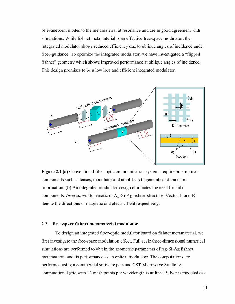
Figure 2.1 (a) Conventional fiber-optic communication systems require bulk optical
components such as lenses, modulator and amplifiers to generate and transport
information. (b) An integrated modulator design eliminates the need for bulk
components. Inset zoom: Schematic of Ag-Si-Ag fishnet structure. Vector H and E
denote the directions of magnetic and electric field respectively.
2.2 Free-space fishnet metamaterial modulator
To design an integrated fiber-optic modulator based on fishnet metamaterial, we
first investigate the free-space modulation effect. Full scale three-dimensional numerical
simulations are performed to obtain the geometric parameters of Ag-Si-Ag fishnet
metamaterial and its performance as an optical modulator. The computations are
performed using a commercial software package CST Microwave Studio. A
computational grid with 12 mesh points per wavelength is utilized. Silver is modeled as a
12
dispersive lossy metal with permittivity governed by Drude model, whereas Si is
modeled as a non-dispersive lossless material with ε =11.9. The structure is embedded in
free-space and is excited by waveguide simulator, which allows modeling of the free-
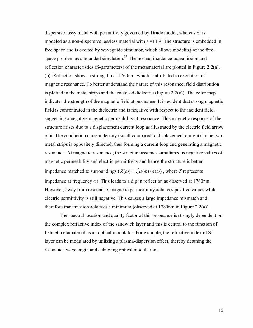
space problem as a bounded simulation.33 The normal incidence transmission and
reflection characteristics (S-parameters) of the metamaterial are plotted in Figure 2.2(a),
(b). Reflection shows a strong dip at 1760nm, which is attributed to excitation of
magnetic resonance. To better understand the nature of this resonance, field distribution
is plotted in the metal strips and the enclosed dielectric (Figure 2.2(c)). The color map
indicates the strength of the magnetic field at resonance. It is evident that strong magnetic
field is concentrated in the dielectric and is negative with respect to the incident field,
suggesting a negative magnetic permeability at resonance. This magnetic response of the
structure arises due to a displacement current loop as illustrated by the electric field arrow
plot. The conduction current density (small compared to displacement current) in the two
metal strips is oppositely directed, thus forming a current loop and generating a magnetic
resonance. At magnetic resonance, the structure assumes simultaneous negative values of
magnetic permeability and electric permittivity and hence the structure is better
impedance matched to surroundings ( ( ) ( ) / ( )Z ω μ ω ε ω= , where Z represents
impedance at frequency ω). This leads to a dip in reflection as observed at 1760nm.
However, away from resonance, magnetic permeability achieves positive values while
electric permittivity is still negative. This causes a large impedance mismatch and
therefore transmission achieves a minimum (observed at 1780nm in Figure 2.2(a)).
The spectral location and quality factor of this resonance is strongly dependent on
the complex refractive index of the sandwich layer and this is central to the function of
fishnet metamaterial as an optical modulator. For example, the refractive index of Si
layer can be modulated by utilizing a plasma-dispersion effect, thereby detuning the
resonance wavelength and achieving optical modulation.
13
Output port
Input port
Output port
Output port
Input port
Input port
1.55 1.60 1.65 1.70 1.75 1.80 1.85 1.90 1.95 2.00
-180
-150
-120
-90
Wavelength (μm)
Phas
e(de
g)
1.55 1.60 1.65 1.70 1.75 1.80 1.85 1.90 1.95 2.00-12
-10
-8
-6
-4
Tra
nsm
issi
on (d
B)
Wavelength (μm)
Transmission (Normal incidence)
(a)
1.55 1.60 1.65 1.70 1.75 1.80 1.85 1.90 1.95 2.00-100-80-60-40-20
0
Wavelength (μm)
1.55 1.60 1.65 1.70 1.75 1.80 1.85 1.90 1.95 2.00
-4
-3
-2
-1
Reflection (Normal incidence)
Phas
e(de
g)R
efle
ctio
n (d
B)
Wavelength (μm)
(b)
14
(c)
Figure 2.2 (a) Normal incidence transmission amplitude and phase characteristics of Ag-
Si-Ag fishnet structure (Inset). (b) Reflection characteristics. (c) Field map within the
metal-dielectric-metal sandwich structure at resonant wavelength of 1760nm. The color
represents magnetic field (H) normalized with respect to incident magnetic field, and the
arrows represent electric field (E) distribution. The incident wave polarization is as
indicated and the dimensional parameters of the fishnet structure as illustrated in Figure
2.1 are tm = 28nm, td = 80nm, dx = 108nm, dy = 250nm, a = b= 550nm.
To investigate the performance of this structure as a free-space optical modulator,
simulations are performed where a pump beam induced modulation in the refractive
index of Si is assumed and transmission characteristics of fishnet are computed (Figure
2.3(a)). It is observed that by modulating the refractive index of Si by just 1.7%,
transmission is modulated by 6dB (75% change) and phase undergoes a shift of 35
degrees (Figure 2.3(b)). In comparison, an equally thick Si layer by itself undergoes a
transmission modulation of less than 0.2dB (4%). It should be noted that this calculation
is performed for just one fishnet layer. This implies that by stacking 5 layers of this
sandwich structure one can build a Mach-Zehnder interferometer with a total interaction
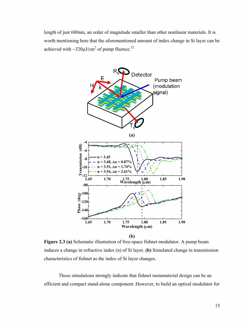
15
length of just 680nm, an order of magnitude smaller than other nonlinear materials. It is
worth mentioning here that the aforementioned amount of index change in Si layer can be
achieved with ~320µJ/cm2 of pump fluence.32
(a)
1.65 1.70 1.75 1.80 1.85 1.90-160
-140
-120
-100
-80
n = 3.45 n = 3.48, Δn = 0.87% n = 3.51, Δn = 1.74% n = 3.54, Δn = 2.61%
1.65 1.70 1.75 1.80 1.85 1.90-12
-10
-8
-6
-4
Wavelength (μm)
Phas
e (d
eg)
Tra
nsm
issi
on (
dB)
Wavelength (μm)
(b)
Figure 2.3 (a) Schematic illustration of free-space fishnet modulator. A pump beam
induces a change in refractive index (n) of Si layer. (b) Simulated change in transmission
characteristics of fishnet as the index of Si layer changes.
These simulations strongly indicate that fishnet metamaterial design can be an
efficient and compact stand-alone component. However, to build an optical modulator for
16
fiber-optic communication systems would require several other bulk components which
to a certain extent nullifies the advantages of a having a compact central unit. By
integrating the modulator directly onto the fiber, we eliminate the bulk optical
components, leading to significant cost reduction. This integrated design offers smaller
footprint, low loss, high efficiency, self-alignment and is less prone to electromagnetic
interference.
2.3 Integrated fishnet metamaterial modulator
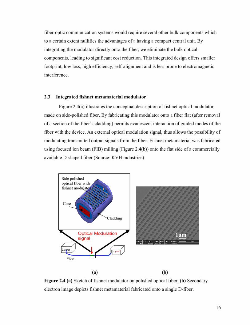
Figure 2.4(a) illustrates the conceptual description of fishnet optical modulator
made on side-polished fiber. By fabricating this modulator onto a fiber flat (after removal
of a section of the fiber’s cladding) permits evanescent interaction of guided modes of the
fiber with the device. An external optical modulation signal, thus allows the possibility of
modulating transmitted output signals from the fiber. Fishnet metamaterial was fabricated
using focused ion beam (FIB) milling (Figure 2.4(b)) onto the flat side of a commercially
available D-shaped fiber (Source: KVH industries).
(a) (b)
Figure 2.4 (a) Sketch of fishnet modulator on polished optical fiber. (b) Secondary
electron image depicts fishnet metamaterial fabricated onto a single D-fiber.
Fiber
Laser
Core
Cladding
Side polished optical fiber with fishnet modulator
Optical Modulation signal
1µm
17
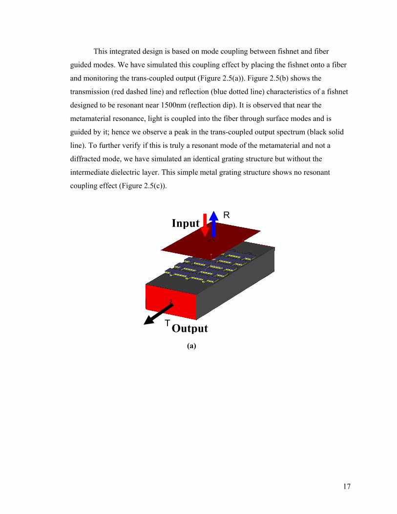
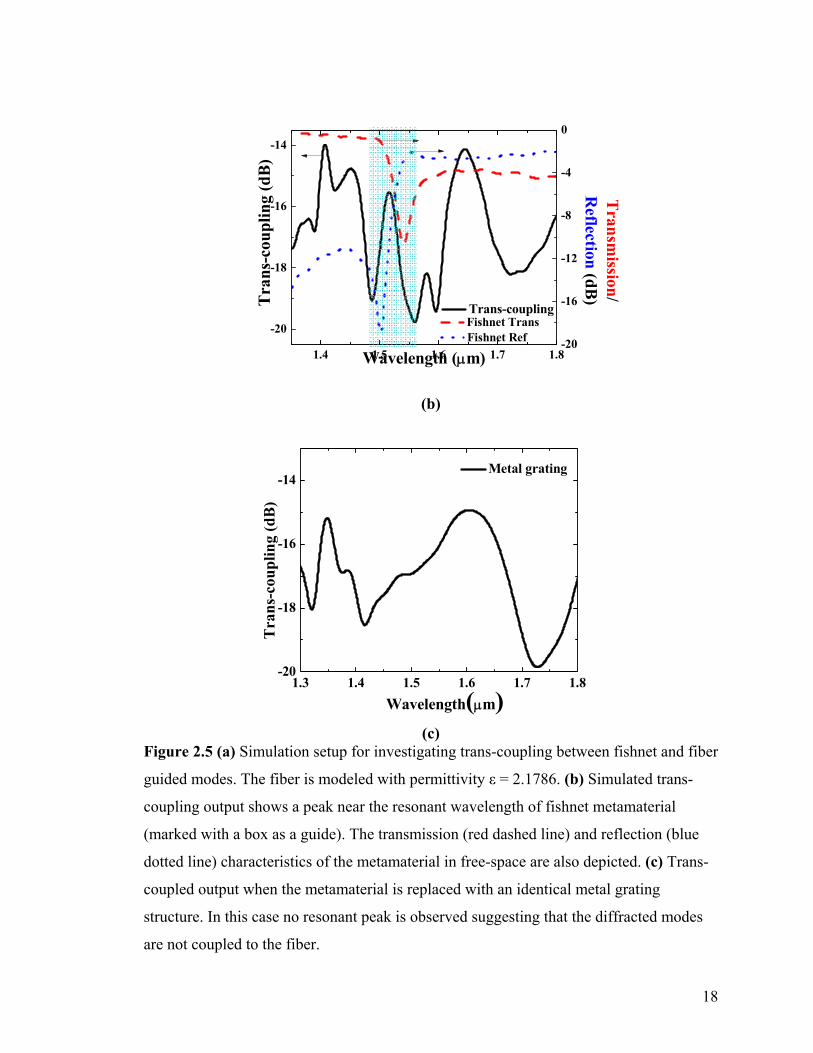
This integrated design is based on mode coupling between fishnet and fiber
guided modes. We have simulated this coupling effect by placing the fishnet onto a fiber
and monitoring the trans-coupled output (Figure 2.5(a)). Figure 2.5(b) shows the
transmission (red dashed line) and reflection (blue dotted line) characteristics of a fishnet
designed to be resonant near 1500nm (reflection dip). It is observed that near the
metamaterial resonance, light is coupled into the fiber through surface modes and is
guided by it; hence we observe a peak in the trans-coupled output spectrum (black solid
line). To further verify if this is truly a resonant mode of the metamaterial and not a
diffracted mode, we have simulated an identical grating structure but without the
intermediate dielectric layer. This simple metal grating structure shows no resonant
coupling effect (Figure 2.5(c)).
(a)
T
RInput
Output
18
1.4 1.5 1.6 1.7 1.8
-20
-18
-16
-14
Transm
ission/R
eflection (dB)T
rans
-cou
plin
g (d
B)
Wavelength (μm)
Trans-coupling
-20
-16
-12
-8
-4
0
Fishnet Trans Fishnet Ref
(b)
1.3 1.4 1.5 1.6 1.7 1.8-20
-18
-16
-14
Tra
ns-c
oupl
ing
(dB
)
Wavelength(μm)
Metal grating
(c)
Figure 2.5 (a) Simulation setup for investigating trans-coupling between fishnet and fiber
guided modes. The fiber is modeled with permittivity ε = 2.1786. (b) Simulated trans-
coupling output shows a peak near the resonant wavelength of fishnet metamaterial
(marked with a box as a guide). The transmission (red dashed line) and reflection (blue
dotted line) characteristics of the metamaterial in free-space are also depicted. (c) Trans-
coupled output when the metamaterial is replaced with an identical metal grating
structure. In this case no resonant peak is observed suggesting that the diffracted modes
are not coupled to the fiber.
19
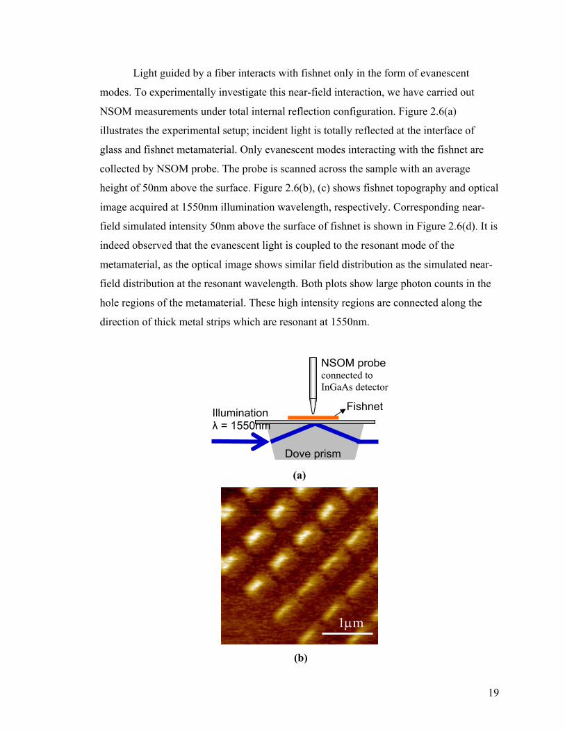
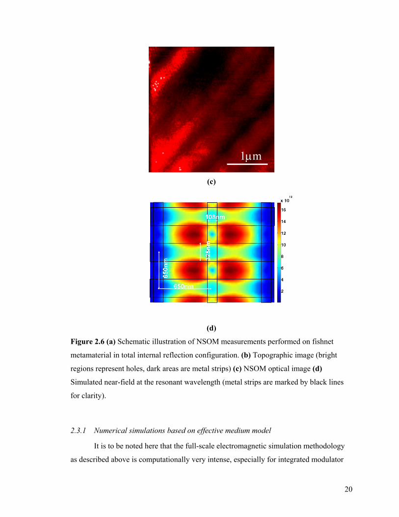
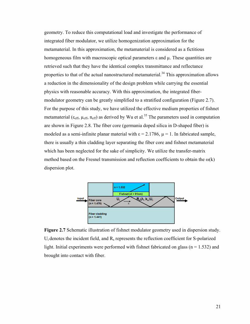
Light guided by a fiber interacts with fishnet only in the form of evanescent
modes. To experimentally investigate this near-field interaction, we have carried out
NSOM measurements under total internal reflection configuration. Figure 2.6(a)
illustrates the experimental setup; incident light is totally reflected at the interface of
glass and fishnet metamaterial. Only evanescent modes interacting with the fishnet are
collected by NSOM probe. The probe is scanned across the sample with an average
height of 50nm above the surface. Figure 2.6(b), (c) shows fishnet topography and optical
image acquired at 1550nm illumination wavelength, respectively. Corresponding near-
field simulated intensity 50nm above the surface of fishnet is shown in Figure 2.6(d). It is
indeed observed that the evanescent light is coupled to the resonant mode of the
metamaterial, as the optical image shows similar field distribution as the simulated near-
field distribution at the resonant wavelength. Both plots show large photon counts in the
hole regions of the metamaterial. These high intensity regions are connected along the
direction of thick metal strips which are resonant at 1550nm.
(a)
(b)
1μm
Illumination λ = 1550nm
Fishnet
Dove prism
NSOM probe connected to InGaAs detector
20
(c)
(d)
Figure 2.6 (a) Schematic illustration of NSOM measurements performed on fishnet
metamaterial in total internal reflection configuration. (b) Topographic image (bright
regions represent holes, dark areas are metal strips) (c) NSOM optical image (d)
Simulated near-field at the resonant wavelength (metal strips are marked by black lines
for clarity).
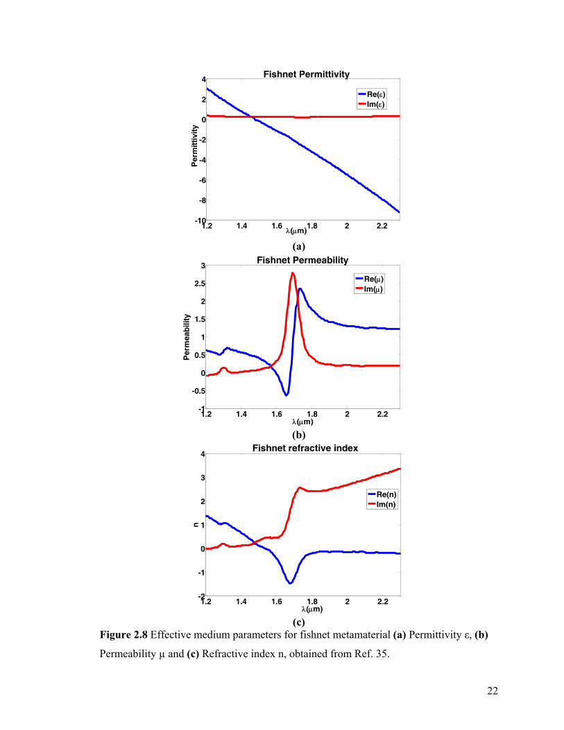
2.3.1 Numerical simulations based on effective medium model
It is to be noted here that the full-scale electromagnetic simulation methodology
as described above is computationally very intense, especially for integrated modulator
1μm
21
geometry. To reduce this computational load and investigate the performance of
integrated fiber modulator, we utilize homogenization approximation for the
metamaterial. In this approximation, the metamaterial is considered as a fictitious
homogeneous film with macroscopic optical parameters ε and µ. These quantities are
retrieved such that they have the identical complex transmittance and reflectance
properties to that of the actual nanostructured metamaterial.34 This approximation allows
a reduction in the dimensionality of the design problem while carrying the essential
physics with reasonable accuracy. With this approximation, the integrated fiber-
modulator geometry can be greatly simplified to a stratified configuration (Figure 2.7).
For the purpose of this study, we have utilized the effective medium properties of fishnet
metamaterial (εeff, µeff, neff) as derived by Wu et al.35 The parameters used in computation
are shown in Figure 2.8. The fiber core (germania doped silica in D-shaped fiber) is
modeled as a semi-infinite planar material with ε = 2.1786, µ = 1. In fabricated sample,
there is usually a thin cladding layer separating the fiber core and fishnet metamaterial
which has been neglected for the sake of simplicity. We utilize the transfer-matrix
method based on the Fresnel transmission and reflection coefficients to obtain the ω(k)
dispersion plot.
Figure 2.7 Schematic illustration of fishnet modulator geometry used in dispersion study.
Ui denotes the incident field, and Rs represents the reflection coefficient for S-polarized
light. Initial experiments were performed with fishnet fabricated on glass (n = 1.532) and
brought into contact with fiber.
22
1.2 1.4 1.6 1.8 2 2.2-10
-8
-6
-4
-2
0
2
4
λ(μm)
Per
mit
tivi
ty
Fishnet Permittivity
Re(ε)Im(ε)
(a)
1.2 1.4 1.6 1.8 2 2.2-1
-0.5
0
0.5
1
1.5
2
2.5
3
λ(μm)
Per
mea
bili
ty
Fishnet Permeability
Re(μ)Im(μ)
(b)
1.2 1.4 1.6 1.8 2 2.2-2
-1
0
1
2
3
4
λ(μm)
n
Fishnet refractive index
Re(n)Im(n)
(c)
Figure 2.8 Effective medium parameters for fishnet metamaterial (a) Permittivity ε, (b)
Permeability µ and (c) Refractive index n, obtained from Ref. 35.
23
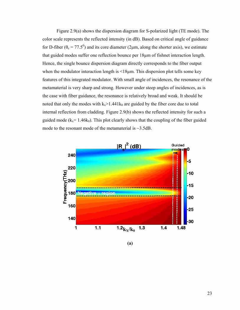
Figure 2.9(a) shows the dispersion diagram for S-polarized light (TE mode). The
color scale represents the reflected intensity (in dB). Based on critical angle of guidance
for D-fiber (θc = 77.50) and its core diameter (2µm, along the shorter axis), we estimate
that guided modes suffer one reflection bounce per 18µm of fishnet interaction length.
Hence, the single bounce dispersion diagram directly corresponds to the fiber output
when the modulator interaction length is <18µm. This dispersion plot tells some key
features of this integrated modulator. With small angle of incidences, the resonance of the
metamaterial is very sharp and strong. However under steep angles of incidences, as is
the case with fiber guidance, the resonance is relatively broad and weak. It should be
noted that only the modes with kx>1.441k0 are guided by the fiber core due to total
internal reflection from cladding. Figure 2.9(b) shows the reflected intensity for such a
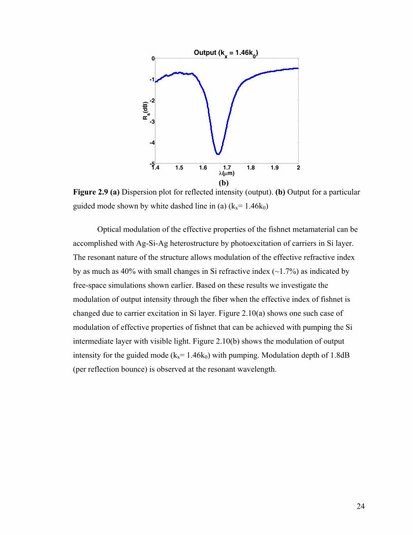
guided mode (kx= 1.46k0). This plot clearly shows that the coupling of the fiber guided
mode to the resonant mode of the metamaterial is ~3.5dB.
(a)
kX/k0
24
1.4 1.5 1.6 1.7 1.8 1.9 2-5
-4
-3
-2
-1
0
λ(μm)
Rs(d
B)
Output (kx = 1.46k
0)
(b)
Figure 2.9 (a) Dispersion plot for reflected intensity (output). (b) Output for a particular
guided mode shown by white dashed line in (a) (kx= 1.46k0)
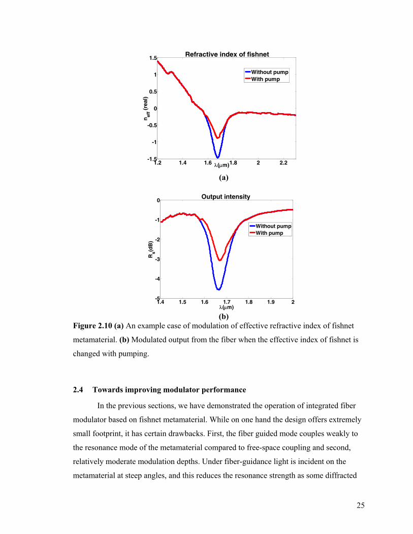
Optical modulation of the effective properties of the fishnet metamaterial can be
accomplished with Ag-Si-Ag heterostructure by photoexcitation of carriers in Si layer.
The resonant nature of the structure allows modulation of the effective refractive index
by as much as 40% with small changes in Si refractive index (~1.7%) as indicated by
free-space simulations shown earlier. Based on these results we investigate the
modulation of output intensity through the fiber when the effective index of fishnet is
changed due to carrier excitation in Si layer. Figure 2.10(a) shows one such case of
modulation of effective properties of fishnet that can be achieved with pumping the Si
intermediate layer with visible light. Figure 2.10(b) shows the modulation of output
intensity for the guided mode (kx= 1.46k0) with pumping. Modulation depth of 1.8dB
(per reflection bounce) is observed at the resonant wavelength.
25
1.2 1.4 1.6 1.8 2 2.2-1.5
-1
-0.5
0
0.5
1
1.5
λ(μm)
nef
f (re
al)
Refractive index of fishnet
Without pumpWith pump
(a)
1.4 1.5 1.6 1.7 1.8 1.9 2-5
-4
-3
-2
-1
0
λ(μm)
Rs(d
B)
Output intensity
Without pumpWith pump
(b)
Figure 2.10 (a) An example case of modulation of effective refractive index of fishnet
metamaterial. (b) Modulated output from the fiber when the effective index of fishnet is
changed with pumping.
2.4 Towards improving modulator performance
In the previous sections, we have demonstrated the operation of integrated fiber
modulator based on fishnet metamaterial. While on one hand the design offers extremely
small footprint, it has certain drawbacks. First, the fiber guided mode couples weakly to
the resonance mode of the metamaterial compared to free-space coupling and second,
relatively moderate modulation depths. Under fiber-guidance light is incident on the
metamaterial at steep angles, and this reduces the resonance strength as some diffracted
26
modes start to propagate through the metamaterial. This is evident from dispersion plot in
Figure 2.9(a) which shows the reduction in resonance strength as the angle of incidence
increases ( 10sin ( / )xk nkθ −= , where θ is the angle of incidence and n is the refractive
index of fiber core). Resonance strength is also low because of losses in the metamaterial
which is also responsible for broadening of resonance. Modulation depth is rather limited
because of the fact that the switching layer is buried underneath a metal film which
requires relatively higher pump intensities to bring the modulation effect. In following
sections, we address these issues and demonstrate that a “flipped fishnet” design is better
suited as an integrated fiber modulator.
2.4.1 Losses, integration of gain material and flipped fishnet for enhanced modulation
One of the most fundamental challenges with the prevalent designs of
metamaterials is the presence of losses. These losses originate from intrinsic absorption
of constituent materials, specifically metals which are highly lossy at optical frequencies.
Resonant nature of the metamaterial and topological effects such as surface roughness
also contributes to the losses. These losses severely hinder the performance of
metamaterials and restrict their range of practical applications. One of the approaches to
compensate loss is inclusion of an optically pumped gain media.36 Gain media can be
incorporated in close proximity of the metamaterial or can be an integral layer of the
metamaterial itself. The former approach was investigated theoretically and
experimentally where an In0.786Ga0.214As0.465P0.535/In0.53Ga0.47As quantum well structure
was used as a substrate providing gain (gain coefficient, g = 3000cm-1) to the fishnet
metamaterial fabricated on top.37 It was observed that even at a nominal gap of 20nm (in
the form of a spacer layer) between the gain media and fishnet metamaterial, the gain had
a very little effect (<2%) on the properties of the metamaterial. This is because
electromagnetic field is concentrated mainly inside the dielectric layer of the fishnet
structure (in between the metal wires, see Figure 2.2(c)) and it penetrates weakly into the
quantum well structure, leading to poor coupling between the metamaterial and
underneath gain media. An alternative to this approach is to replace the passive dielectric
layer in fishnet metamaterial with active gain media. This can be accomplished by using
27
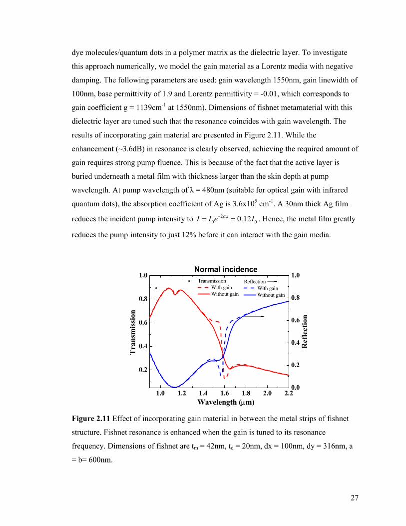
dye molecules/quantum dots in a polymer matrix as the dielectric layer. To investigate
this approach numerically, we model the gain material as a Lorentz media with negative
damping. The following parameters are used: gain wavelength 1550nm, gain linewidth of
100nm, base permittivity of 1.9 and Lorentz permittivity = -0.01, which corresponds to
gain coefficient g = 1139cm-1 at 1550nm). Dimensions of fishnet metamaterial with this
dielectric layer are tuned such that the resonance coincides with gain wavelength. The
results of incorporating gain material are presented in Figure 2.11. While the
enhancement (~3.6dB) in resonance is clearly observed, achieving the required amount of
gain requires strong pump fluence. This is because of the fact that the active layer is
buried underneath a metal film with thickness larger than the skin depth at pump
wavelength. At pump wavelength of λ = 480nm (suitable for optical gain with infrared
quantum dots), the absorption coefficient of Ag is 3.6x105 cm-1. A 30nm thick Ag film
reduces the incident pump intensity to 20 00.12zI I e Iα−= = . Hence, the metal film greatly
reduces the pump intensity to just 12% before it can interact with the gain media.
1.0 1.2 1.4 1.6 1.8 2.0 2.2
0.2
0.4
0.6
0.8
1.0
Tra
nsm
issi
on
Ref
lect
ion
Wavelength (μm)
Transmission With gain Without gain
0.0
0.2
0.4
0.6
0.8
1.0Reflection
With gain Without gain
Normal incidence
Figure 2.11 Effect of incorporating gain material in between the metal strips of fishnet
structure. Fishnet resonance is enhanced when the gain is tuned to its resonance
frequency. Dimensions of fishnet are tm = 42nm, td = 20nm, dx = 100nm, dy = 316nm, a
= b= 600nm.
28
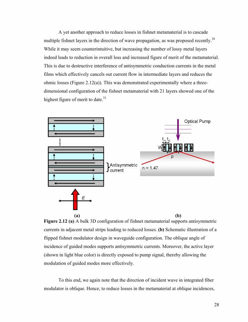
A yet another approach to reduce losses in fishnet metamaterial is to cascade
multiple fishnet layers in the direction of wave propagation, as was proposed recently.38
While it may seem counterintuitive, but increasing the number of lossy metal layers
indeed leads to reduction in overall loss and increased figure of merit of the metamaterial.
This is due to destructive interference of antisymmetric conduction currents in the metal
films which effectively cancels out current flow in intermediate layers and reduces the
ohmic losses (Figure 2.12(a)). This was demonstrated experimentally where a three-
dimensional configuration of the fishnet metamaterial with 21 layers showed one of the
highest figure of merit to date.31
(a) (b)
Figure 2.12 (a) A bulk 3D configuration of fishnet metamaterial supports antisymmetric
currents in adjacent metal strips leading to reduced losses. (b) Schematic illustration of a
flipped fishnet modulator design in waveguide configuration. The oblique angle of
incidence of guided modes supports antisymmetric currents. Moreover, the active layer
(shown in light blue color) is directly exposed to pump signal, thereby allowing the
modulation of guided modes more effectively.
To this end, we again note that the direction of incident wave in integrated fiber
modulator is oblique. Hence, to reduce losses in the metamaterial at oblique incidences,
29
we have investigated a novel approach. In this approach, the individual magnetic
resonator unit of fishnet is flipped (Figure 2.12(b)). As the wave propagates through the
fiber, the individual flipped units experience different phase, which allows the metal
films to have antisymmetric currents and hence low loss. This design also offers an
enhanced modulation effect as the switching media is directly exposed to pump radiation,
thereby improving the overall efficiency of integrated modulator.
2.4.2 Oblique angle simulations of flipped fishnet
To quantitatively understand the behavior of flipped fishnet when integrated onto
a fiber, we have performed numerical simulations at oblique incidences. While methods
of simulating metamaterials at normal incidence using finite-difference time-domain
(FDTD) are well established,33 broadband off-normal incidence simulations pose a
unique problem to FDTD approach. In broadband simulations, the source injects a field
with a constant in-plane wavevector for all frequencies. This implies that the actual
injection angle varies as a function of frequency. Multiple simulations are required to
gather simulation data at various frequencies for a fixed angle of incidence.39, 40 We have
investigated the flipped metal-dielectric-metal resonator design at oblique angles of
incidence. A parametric sweep for various angles of incidence is done within the
wavelength range of interest. Bloch boundary conditions are used along the periodic
direction of the metamaterial. For simplicity, we have considered a two-dimensional case
where the electric rods such as in fishnet design are eliminated. The data obtained from
these simulations is irregularly spaced and has been interpolated to a rectangular grid of
angle of incidence and wavelength for ease of plotting.
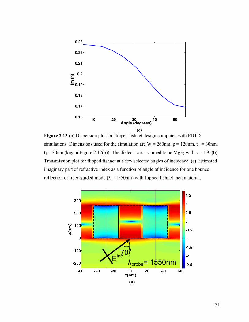
Figure 2.13(a) shows the dispersion plot of transmission response of flipped
resonators against frequency and angle of incidence. It is observed that the resonance
becomes narrower with increased angle of incidence (Figure 2.13(b)). This is attributed to
reduced losses as increasing oblique incidences start to support antiphase currents in
adjacent units of flipped resonators. To further quantify this effect, we have estimated the
losses through the flipped fishnet as a function of angle of incidence. This is achieved by
calculating imaginary part of refractive index 1Im( ) ln( )4
RnW Tλπ
−= ,31 where W is the
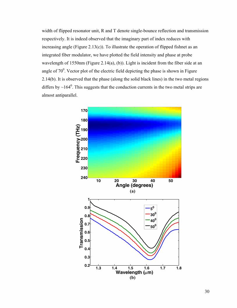
30
width of flipped resonator unit, R and T denote single-bounce reflection and transmission
respectively. It is indeed observed that the imaginary part of index reduces with
increasing angle (Figure 2.13(c)). To illustrate the operation of flipped fishnet as an
integrated fiber modulator, we have plotted the field intensity and phase at probe
wavelength of 1550nm (Figure 2.14(a), (b)). Light is incident from the fiber side at an
angle of 700. Vector plot of the electric field depicting the phase is shown in Figure
2.14(b). It is observed that the phase (along the solid black lines) in the two metal regions
differs by ~1640. This suggests that the conduction currents in the two metal strips are
almost antiparallel.
Angle (degrees)
Fre
qu
ency
(T
Hz)
10 20 30 40 50
170
180
190
200
210
220
230
240
(a)
1.3 1.4 1.5 1.6 1.7 1.80.2
0.3
0.4
0.5
0.6
0.7
0.8
0.9
1
Wavelength (μm)
Tra
nsm
issi
on
50
300
400
500
(b)
31
10 20 30 40 500.16
0.17
0.18
0.19
0.2
0.21
0.22
0.23
Angle (degrees)
Im (
n)
(c)
Figure 2.13 (a) Dispersion plot for flipped fishnet design computed with FDTD
simulations. Dimensions used for the simulation are W = 260nm, p = 120nm, tm = 30nm,
td = 30nm (key in Figure 2.12(b)). The dielectric is assumed to be MgF2 with ε = 1.9. (b)
Transmission plot for flipped fishnet at a few selected angles of incidence. (c) Estimated
imaginary part of refractive index as a function of angle of incidence for one bounce
reflection of fiber-guided mode (λ = 1550nm) with flipped fishnet metamaterial.
(a)
Einc700
λprobe= 1550nm
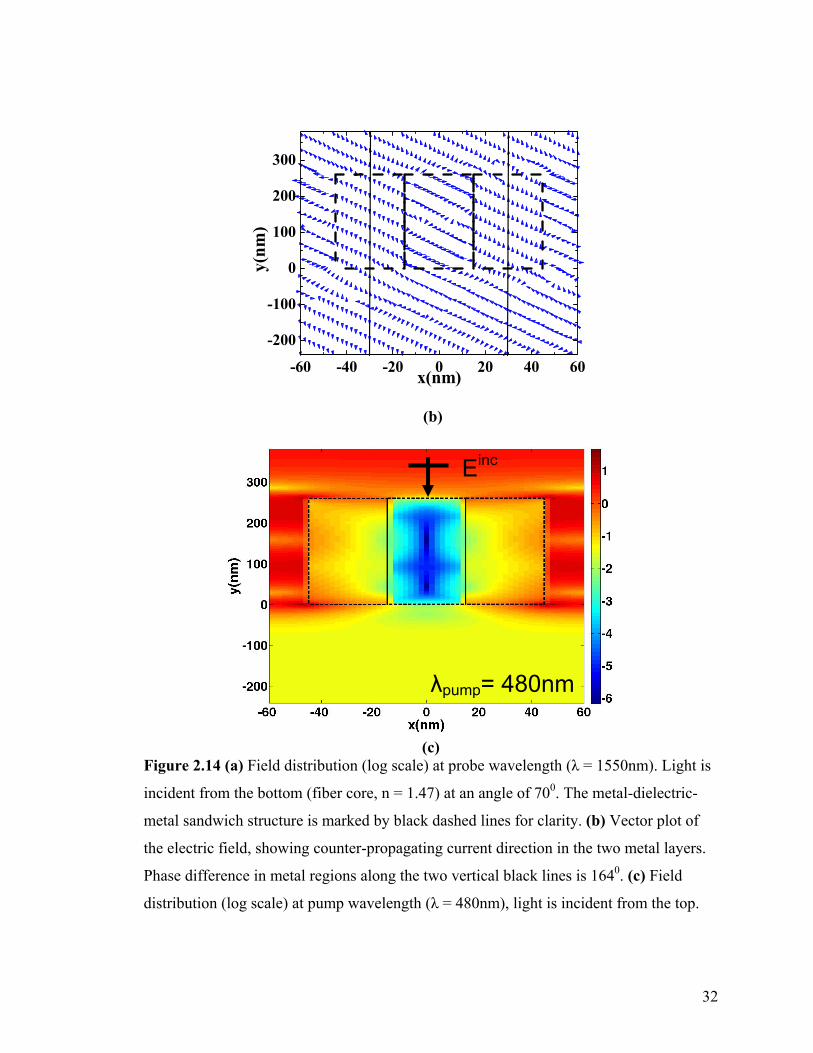
32
-60 -40 -20 0 20 40 60
-200
-100
0
100
200
300
y(nm
)
x(nm)
(b)
(c)
Figure 2.14 (a) Field distribution (log scale) at probe wavelength (λ = 1550nm). Light is
incident from the bottom (fiber core, n = 1.47) at an angle of 700. The metal-dielectric-
metal sandwich structure is marked by black dashed lines for clarity. (b) Vector plot of
the electric field, showing counter-propagating current direction in the two metal layers.
Phase difference in metal regions along the two vertical black lines is 1640. (c) Field
distribution (log scale) at pump wavelength (λ = 480nm), light is incident from the top.
λpump= 480nm
Einc
33
To investigate the switching ratio of this integrated modulator in presence of a
gain medium, we have plotted the field distribution at the pump wavelength (480nm) in
Figure 2.14(c). Pump radiation is incident from the top which efficiently excites the gain
layer sandwiched in between the two metal strips. The field distribution suggests that the
pump field penetrates weakly into the fiber-core; however, the probe field interacts
strongly with the gain layer (Figure 2.14(a)). Upon absorption of pump radiation, the gain
layer provides optical amplification to the probe field. We observe that with moderate
gain coefficients (g = 1139cm-1), the reflected intensity for guided mode (λ = 1550nm) is
modulated by 2.05dB (37%) when pump radiation is turned on. This is significantly
better compared to the case, where gain is incorporated into substrate.37 With less than
half the amount of gain required the modulation is improved by more than 35%.
Moreover, the required amount of gain in flipped fishnet can be achieved with less than
12% of pump power compared to reported fishnet structure, where the metal film is
exposed to pump radiation.
2.5 Summary
To summarize, in this study we have investigated fishnet metamaterial as an
optical modulator for on-fiber communication and information processing applications.
This design offers small footprint (~10λ) and integration on fiber eliminates the need for
bulk optical components. Numerical studies indicate an on/off ratio of 1.8dB for the
integrated modulator. To reduce the losses associated with fishnet metamaterial and
improve coupling to fiber guided modes, we have investigated a flipped fishnet design
which has metal-dielectric-metal sandwich in a direction perpendicular to conventional
fishnet. This design offers several advantages: Reduction in ohmic losses, as the
antisymmetric currents in adjacent metal strips lead to destructive interference at oblique
incidences; secondly, enhanced modulation effect, as the switching layer is directly
exposed to pump radiation. With less than 12% of incident pump power compared to
conventional fishnet, flipped fishnet shows a modulation depth of 2.05dB of fiber guided
modes. This small footprint, high efficiency metamaterial opens exciting avenues for
telecommunication applications.
34
3 IMAGING OF PLASMONIC MODES OF NANOSTRUCTURES USING
HIGH-RESOLUTION CATHODOLUMINESCENE SPECTROSCOPY
3.1 Introduction
A multitude of optical phenomena at the nanoscale are made possible by resonant
surface plasmons in artificially structured metal systems. These optical phenomena often
give rise to properties that are difficult to obtain in natural materials. An entire new
generation of artificial materials in the emerging field of plasmonics is designed to
harness these properties through nanoscale engineering. These materials find tremendous
applications in chemical and biological sensing.41, 42 By simple surface patterning a thin
metal film, it is possible to engineer its surface modes over a wide range of frequency.23
Highly localized optical modes associated with patterned surfaces with nanoscale features
(<~200nm) and the sensitivity of these modes to local refractive index finds tremendous
potential in realizing compatible and efficient sensors. These optical modes known as
localized surface plasmon resonance (LSPR) modes are responsible for producing strong
scattering and extinction spectra in metal nanoparticles such as silver and gold.
Exploiting local electromagnetic field enhancement associated with these plasmonic
structures has led to several interesting applications such as enhanced fluorescence,43
enhanced photo-carrier generation44 and other nonlinear effects such as second
harmonic45 and high-harmonic generation46. Often the field is confined spatially on
length scales on the order of 10-50nm and varies strongly with particle shape, size and
material composition.47 Unfortunately, diffraction-limited optical imaging techniques do
not have enough spatial resolution to image these plasmon modes or precisely locate the
“hot-spots” responsible for producing enormous enhancement such as in Raman imaging.
Near-field scanning optical microscopy (NSOM) has been used to investigate these
plasmon modes,48 however, the resolution is limited by the tip size (~50-100nm). On the
other hand, electron beam based characterization techniques such as
cathodoluminescence (CL) and electron energy loss spectroscopy (EELS) are able to
excite and image plasmon modes with very high spatial resolution. EELS for example has
been demonstrated to resolve plasmon modes on length scale below 18nm.49 EELS
35
technique, however, has to be performed in a transmission electron microscope (TEM),
where it detects the inelastically scattered electrons and the loss suffered by electron
beam in exciting surface plasmons. Although the technique has been described as one
with the best spatial and energy resolution,49 it requires samples to be electron transparent
(typically <100nm). Specialized sample preparation procedure (used for TEM) and
instrumentation makes it an expensive alternative and infeasible for samples on thick
substrate. On the other hand, scanning electron microscopy (SEM) based CL technique
does not suffer from this limitation. CL (in both SEM and TEM mode) has been utilized
to image plasmon modes of particles and antennas of various shapes.50-53
CL has been used in materials science as an advanced technique for examination
of intrinsic structures of semiconductors such as quantum wells54, 55 or quantum dots56, 57.
Typically, a tightly focused beam of electrons impinges on a sample and induces it to
emit light from a localized area down to 10-20 nanometers in size. By scanning the
electron beam in an X-Y pattern and measuring the wavelength and intensity of light
emitted with the focused electron beam at each point, a high resolution map of the optical
activity of the specimen can be obtained. In traditional cathodoluminescence of
semiconductors, impingement of a high energy electron beam will result in the excitation
of valence electrons into the conduction band, leaving behind a hole. The detected photon
emission is actually a result of electron-hole recombination process. In the case of
metallic nanostructures however, the photons are produced as a result of excited
plasmons, i.e. collective motion of the conduction electrons induced by the fast moving
electrons, and these induced charges can act back on the electron beam, causing it to lose
energy as detected in EELS. In CL spectroscopy, we are able to detect radiation due to
the oscillating plasmon on metallic structures, allowing quantitative study of the local
field (Figure 3.1). Mechanism of this radiation has recently been presented52, 58. While,
photon emission from semiconductor materials on interaction with electron beam is well
understood, CL from plasmonic nanostructures is a relatively new field and deserves
more attention.
36
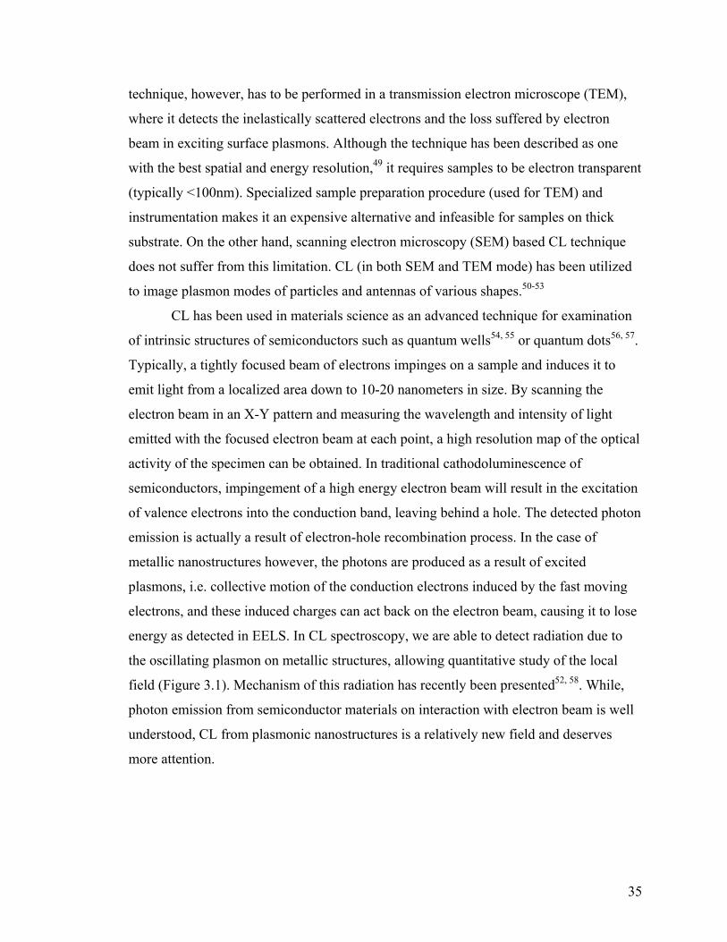
Figure 3.1 Schematic illustration of CL spectroscopy and imaging technique performed
in scanning electron microscope. Inset: Passing electron beam induces
current/electromagnetic oscillations in a metallic particle. These oscillations known as
surface plasmon modes are responsible for radiation detected in CL.
In this study, we investigate the plasmon modes of silver (Ag) triangular
nanoparticles using CL imaging and spectroscopy. The triangular particle geometry is of
special interest to chemists and a hexagonal array of these particles has been extensively
studied as a surface-enhanced Raman spectroscopy (SERS) substrate.59, 60 It has been
shown that Raman signal of molecules adsorbed on these particles can be enhanced by a
factor of 108.59 While it is understood that the excitation of plasmons in these metallic
nanoparticles is responsible for the field enhancement effect, it is a challenge to identify
the local fields associated with these plasmons. Several theoretical studies have identified
the plasmon eigenmodes of triangular nanoparticles,61-63 only a few experimental studies
have demonstrated a resolution capability of mapping the spatial field variation
associated with these plasmon modes.49, 64, 65 In this work, we report direct excitation and
emission of decoupled surface plasmon modes with CL spectroscopy (in SEM chamber)
on triangular nanoparticles. In spectroscopic mode with monochromatic photon maps, we
are able to distinguish the dramatic spatial variation of resonant plasmon mode on length
scales smaller than 25nm. Numerical simulations were performed to identify the plasmon
eigenmodes of triangular particles using a commercial finite-difference time-domain
37
(FDTD) simulator.40 Both electron beam excitation and a more conventional plane wave
scattering type calculations are performed to stress the differences between light
excitation and electron excitation. Electron excitation calculations are performed by
modeling the moving electron charge as a series of closely spaced dipoles with temporal
phase delay governed by the velocity of electron. We also incorporate substrate effect
into our calculations. We illustrate that while normally incident light can excite in-plane
eigenmodes, electron beam is capable of exciting out of plane dipole mode of the
particles.
3.2 Results and discussion
Conventionally, nanoparticles are characterized by their extinction spectra. The
peaks observed in absorption or scattering spectra of particles under light excitation
reveal resonant wavelengths of certain plasmon eigenmodes of the particle. While light
excitation can couple to low frequency plasmon eigenmodes, it is hard to excite high-
frequency plasmon states due to large momentum mismatch.66 Electron excitation on the
other hand can couple to high-frequency plasmon modes and recently it has been
described to directly reveal the local density of plasmon states.67 While optical techniques
are limited in their resolution capability to image the plasmon eigenmodes, electron
excitation on the other hand is potentially capable of resolving details below 10s of
nanometers. Resolving surface plasmon modes and understanding the underlying physics
is crucial to design better plasmonic devices tailored to specific applications.
For the purpose of this study we fabricated 40nm thick Ag equilateral triangular
nanoparticles with ~200nm edge length arranged in a hexagonal lattice (as in SERS
studies60). These particles are fabricated on silicon substrate and the shortest distance
between two adjacent particles is >100nm. Silicon is chosen as the substrate material, to
suppress background cathodoluminescence in the wavelength range of interest (near-UV
and visible). For the purpose of numerical simulations we model and analyze single
nanoparticle. This is because experimentally the interaction distance between electron
beam and the particle is limited to few 10’s of nms and hence, the excitation of plasmon
modes is insensitive to particle coupling over ~100nm spacing. This is especially true for
38
particles on a non-plasmonic substrate such as silicon. We have performed spectrally
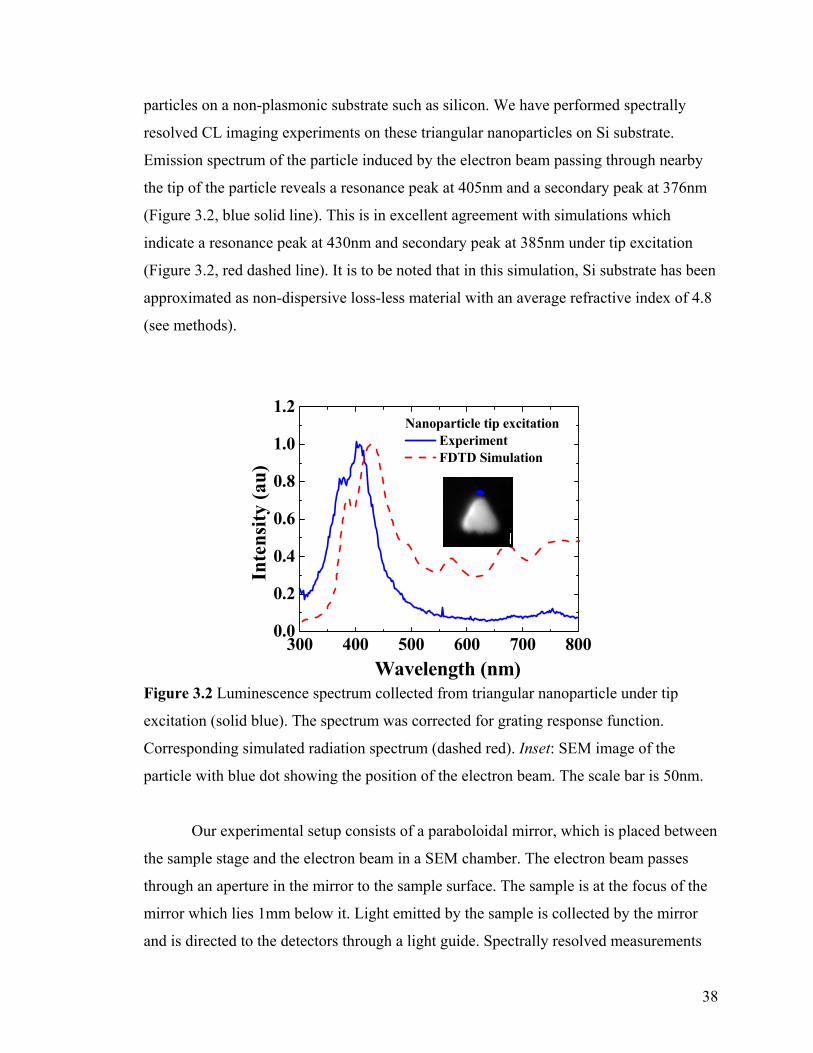
resolved CL imaging experiments on these triangular nanoparticles on Si substrate.
Emission spectrum of the particle induced by the electron beam passing through nearby
the tip of the particle reveals a resonance peak at 405nm and a secondary peak at 376nm
(Figure 3.2, blue solid line). This is in excellent agreement with simulations which
indicate a resonance peak at 430nm and secondary peak at 385nm under tip excitation
(Figure 3.2, red dashed line). It is to be noted that in this simulation, Si substrate has been
approximated as non-dispersive loss-less material with an average refractive index of 4.8
(see methods).
300 400 500 600 700 8000.0
0.2
0.4
0.6
0.8
1.0
1.2
Inte
nsity
(au)
Wavelength (nm)
Nanoparticle tip excitation Experiment FDTD Simulation
Figure 3.2 Luminescence spectrum collected from triangular nanoparticle under tip
excitation (solid blue). The spectrum was corrected for grating response function.
Corresponding simulated radiation spectrum (dashed red). Inset: SEM image of the
particle with blue dot showing the position of the electron beam. The scale bar is 50nm.
Our experimental setup consists of a paraboloidal mirror, which is placed between
the sample stage and the electron beam in a SEM chamber. The electron beam passes
through an aperture in the mirror to the sample surface. The sample is at the focus of the
mirror which lies 1mm below it. Light emitted by the sample is collected by the mirror
and is directed to the detectors through a light guide. Spectrally resolved measurements
39
are performed using a monochromator (Czerny-Turner type). Light passing through a
monochromator allows taking a spectrum, as well as images at a selected wavelength. In
panchromatic mode of imaging, light skips the monochromator and all of the light is
carried to the detection optics. The measurements are performed using a 15kV electron
beam and a photo multiplier tube (PMT) detector with sensitivity encompassing near-
ultraviolet (UV) and visible wavelengths (250-850nm).
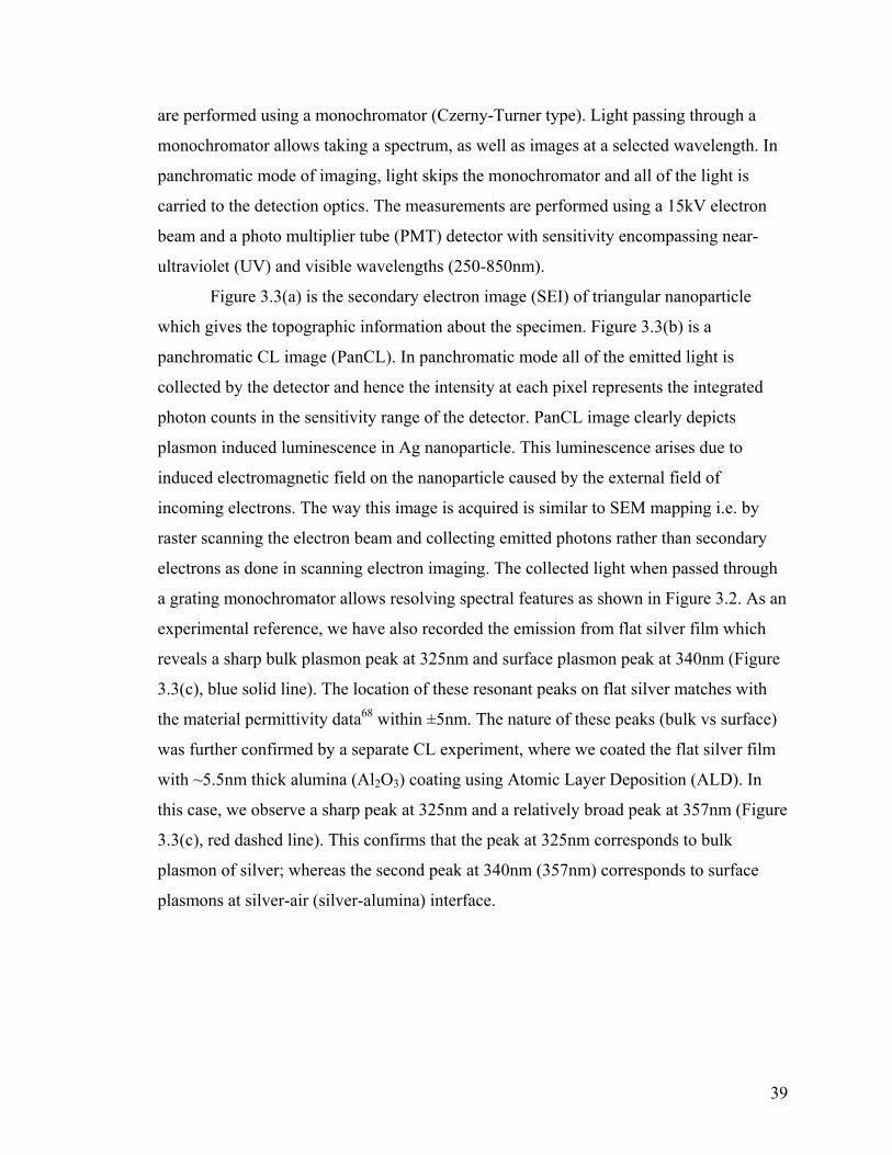
Figure 3.3(a) is the secondary electron image (SEI) of triangular nanoparticle
which gives the topographic information about the specimen. Figure 3.3(b) is a
panchromatic CL image (PanCL). In panchromatic mode all of the emitted light is
collected by the detector and hence the intensity at each pixel represents the integrated
photon counts in the sensitivity range of the detector. PanCL image clearly depicts
plasmon induced luminescence in Ag nanoparticle. This luminescence arises due to
induced electromagnetic field on the nanoparticle caused by the external field of
incoming electrons. The way this image is acquired is similar to SEM mapping i.e. by
raster scanning the electron beam and collecting emitted photons rather than secondary
electrons as done in scanning electron imaging. The collected light when passed through
a grating monochromator allows resolving spectral features as shown in Figure 3.2. As an
experimental reference, we have also recorded the emission from flat silver film which
reveals a sharp bulk plasmon peak at 325nm and surface plasmon peak at 340nm (Figure
3.3(c), blue solid line). The location of these resonant peaks on flat silver matches with
the material permittivity data68 within ±5nm. The nature of these peaks (bulk vs surface)
was further confirmed by a separate CL experiment, where we coated the flat silver film
with ~5.5nm thick alumina (Al2O3) coating using Atomic Layer Deposition (ALD). In
this case, we observe a sharp peak at 325nm and a relatively broad peak at 357nm (Figure
3.3(c), red dashed line). This confirms that the peak at 325nm corresponds to bulk
plasmon of silver; whereas the second peak at 340nm (357nm) corresponds to surface
plasmons at silver-air (silver-alumina) interface.
40
(a) (b)
300 400 500 6000
100
200
300
400
500
Inte
nsity
(au)
Wavelength (nm)
CL on flat silver film 5.5nm Al2O3 coated film
(c)
Figure 3.3 (a) Scanning electron micrograph of triangular nanoparticle. (b) Panchromatic
CL image of the same. (c) Luminescence spectrum collected from a flat silver film.
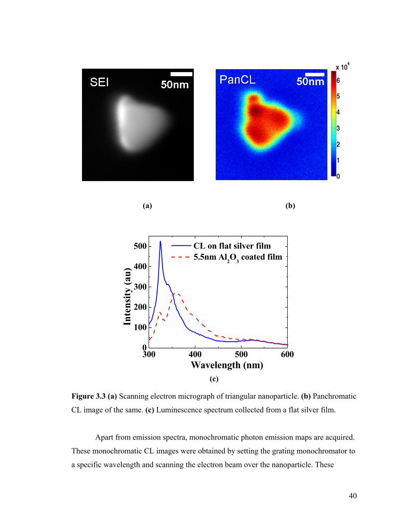
Apart from emission spectra, monochromatic photon emission maps are acquired.
These monochromatic CL images were obtained by setting the grating monochromator to
a specific wavelength and scanning the electron beam over the nanoparticle. These
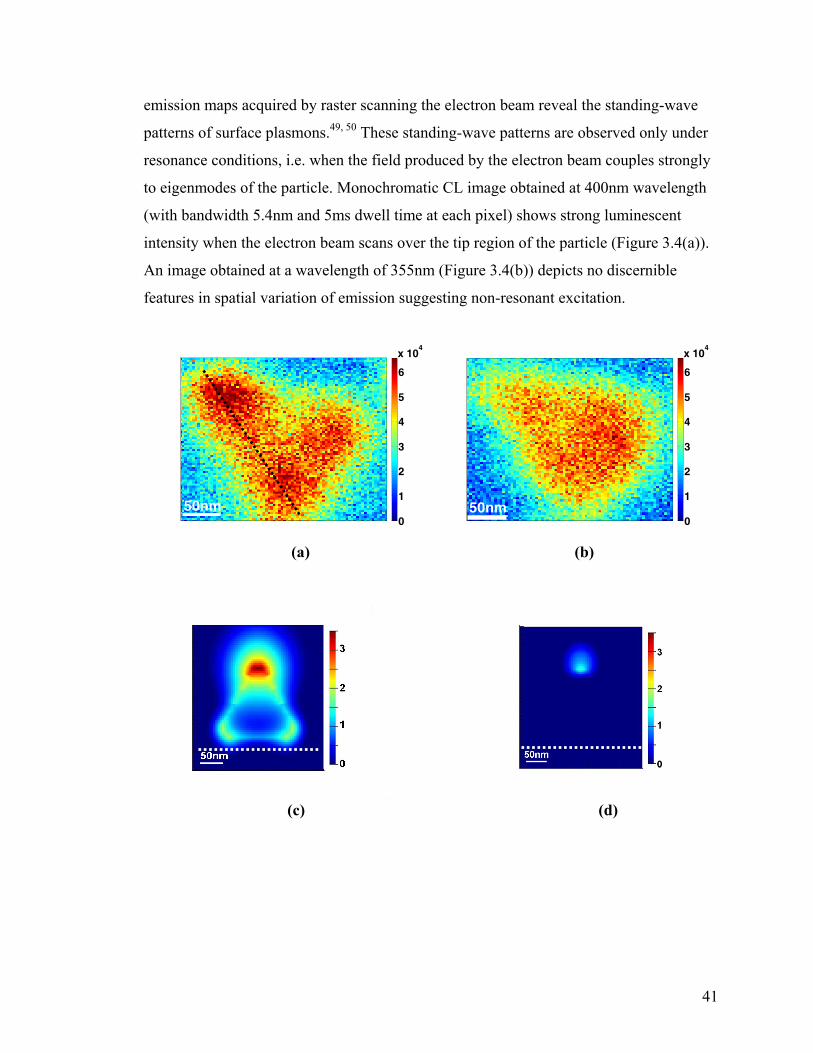
41
emission maps acquired by raster scanning the electron beam reveal the standing-wave
patterns of surface plasmons.49, 50 These standing-wave patterns are observed only under
resonance conditions, i.e. when the field produced by the electron beam couples strongly
to eigenmodes of the particle. Monochromatic CL image obtained at 400nm wavelength
(with bandwidth 5.4nm and 5ms dwell time at each pixel) shows strong luminescent
intensity when the electron beam scans over the tip region of the particle (Figure 3.4(a)).
An image obtained at a wavelength of 355nm (Figure 3.4(b)) depicts no discernible
features in spatial variation of emission suggesting non-resonant excitation.
0
1
2
3
4
5
6
x 104
50nm
0
1
2
3
4
5
6
x 104
50nm
(a) (b)
(c) (d)
42
-100 -80 -60 -40 -20 0 20 40 60 80 100-50
-30
-10
10
30
50
X(nm)
Z(n
m)
+
- -
-100 -80 -60 -40 -20 0 20 40 60 80 100-50
-30
-10
10
30
50
X(nm)
Z(n
m)
(e) (f)
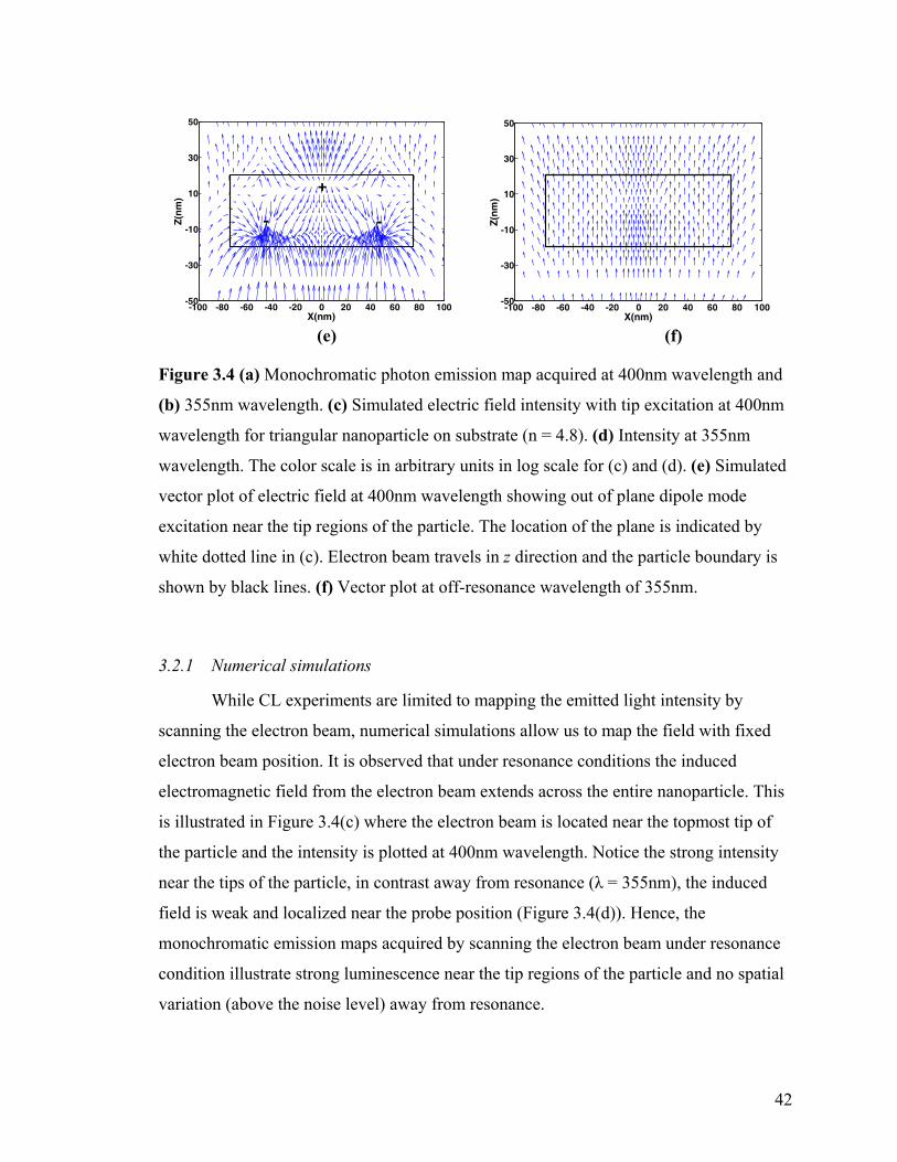
Figure 3.4 (a) Monochromatic photon emission map acquired at 400nm wavelength and
(b) 355nm wavelength. (c) Simulated electric field intensity with tip excitation at 400nm
wavelength for triangular nanoparticle on substrate (n = 4.8). (d) Intensity at 355nm
wavelength. The color scale is in arbitrary units in log scale for (c) and (d). (e) Simulated
vector plot of electric field at 400nm wavelength showing out of plane dipole mode
excitation near the tip regions of the particle. The location of the plane is indicated by
white dotted line in (c). Electron beam travels in z direction and the particle boundary is
shown by black lines. (f) Vector plot at off-resonance wavelength of 355nm.
3.2.1 Numerical simulations
While CL experiments are limited to mapping the emitted light intensity by
scanning the electron beam, numerical simulations allow us to map the field with fixed
electron beam position. It is observed that under resonance conditions the induced
electromagnetic field from the electron beam extends across the entire nanoparticle. This
is illustrated in Figure 3.4(c) where the electron beam is located near the topmost tip of
the particle and the intensity is plotted at 400nm wavelength. Notice the strong intensity
near the tips of the particle, in contrast away from resonance (λ = 355nm), the induced
field is weak and localized near the probe position (Figure 3.4(d)). Hence, the
monochromatic emission maps acquired by scanning the electron beam under resonance
condition illustrate strong luminescence near the tip regions of the particle and no spatial
variation (above the noise level) away from resonance.
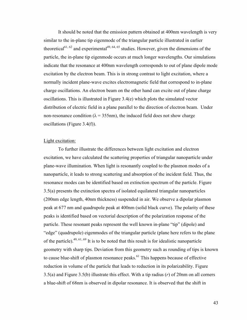
43
It should be noted that the emission pattern obtained at 400nm wavelength is very
similar to the in-plane tip eigenmode of the triangular particle illustrated in earlier
theoretical61, 62 and experimental49, 64, 65 studies. However, given the dimensions of the
particle, the in-plane tip eigenmode occurs at much longer wavelengths. Our simulations
indicate that the resonance at 400nm wavelength corresponds to out of plane dipole mode
excitation by the electron beam. This is in strong contrast to light excitation, where a
normally incident plane-wave excites electromagnetic field that correspond to in-plane
charge oscillations. An electron beam on the other hand can excite out of plane charge
oscillations. This is illustrated in Figure 3.4(e) which plots the simulated vector
distribution of electric field in a plane parallel to the direction of electron beam. Under
non-resonance condition (λ = 355nm), the induced field does not show charge
oscillations (Figure 3.4(f)).
Light excitation:
To further illustrate the differences between light excitation and electron
excitation, we have calculated the scattering properties of triangular nanoparticle under
plane-wave illumination. When light is resonantly coupled to the plasmon modes of a
nanoparticle, it leads to strong scattering and absorption of the incident field. Thus, the
resonance modes can be identified based on extinction spectrum of the particle. Figure
3.5(a) presents the extinction spectra of isolated equilateral triangular nanoparticles
(200nm edge length, 40nm thickness) suspended in air. We observe a dipolar plasmon
peak at 677 nm and quadrupole peak at 400nm (solid black curve). The polarity of these
peaks is identified based on vectorial description of the polarization response of the
particle. These resonant peaks represent the well known in-plane “tip” (dipole) and
“edge” (quadrupole) eigenmodes of the triangular particle (plane here refers to the plane
of the particle).49, 61, 69 It is to be noted that this result is for idealistic nanoparticle
geometry with sharp tips. Deviation from this geometry such as rounding of tips is known
to cause blue-shift of plasmon resonance peaks.61 This happens because of effective
reduction in volume of the particle that leads to reduction in its polarizability. Figure
3.5(a) and Figure 3.5(b) illustrate this effect. With a tip radius (r) of 20nm on all corners
a blue-shift of 68nm is observed in dipolar resonance. It is observed that the shift in
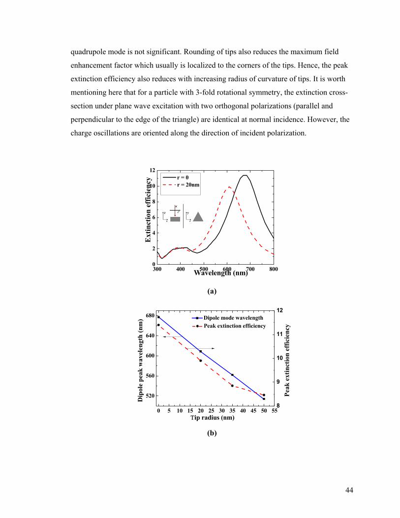
44
quadrupole mode is not significant. Rounding of tips also reduces the maximum field
enhancement factor which usually is localized to the corners of the tips. Hence, the peak
extinction efficiency also reduces with increasing radius of curvature of tips. It is worth
mentioning here that for a particle with 3-fold rotational symmetry, the extinction cross-
section under plane wave excitation with two orthogonal polarizations (parallel and
perpendicular to the edge of the triangle) are identical at normal incidence. However, the
charge oscillations are oriented along the direction of incident polarization.
300 400 500 600 700 8000
2
4
6
8
10
12
Ext
inct
ion
effic
ienc
y
Wavelength (nm)
r = 0 r = 20nm
(a)
0 5 10 15 20 25 30 35 40 45 50 55
520
560
600
640
680 Dipole mode wavelength
Peak
ext
inct
ion
effic
ienc
y
Dip
ole
peak
wav
elen
gth
(nm
)
Τip radius (nm)
8
9
10
11
12
Peak extinction efficiency
(b)
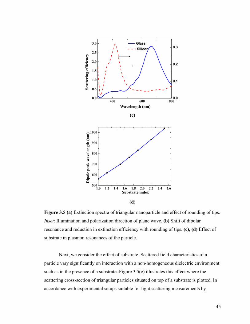
45
400 600 8000.0
0.5
1.0
1.5
2.0
2.5
3.0
Scat
teri
ng e
ffic
ienc
y
Wavelength (nm)
Glass
0.0
0.1
0.2
0.3 Silicon
(c)
1.0 1.2 1.4 1.6 1.8 2.0 2.2 2.4 2.6500
600
700
800
900
1000
Dip
ole
peak
wav
elen
gth
(nm
)
Substrate index
(d)
Figure 3.5 (a) Extinction spectra of triangular nanoparticle and effect of rounding of tips.
Inset: Illumination and polarization direction of plane wave. (b) Shift of dipolar
resonance and reduction in extinction efficiency with rounding of tips. (c), (d) Effect of
substrate in plasmon resonances of the particle.
Next, we consider the effect of substrate. Scattered field characteristics of a
particle vary significantly on interaction with a non-homogeneous dielectric environment
such as in the presence of a substrate. Figure 3.5(c) illustrates this effect where the
scattering cross-section of triangular particles situated on top of a substrate is plotted. In
accordance with experimental setups suitable for light scattering measurements by
46
particles on a substrate, we incorporate light incidence from the top (air side) and only the
scattered power in top half plane is considered in the calculations. It is observed that the
dipolar resonance of the particle on a substrate is red-shifted with respect to its free-space
resonance (Figure 3.5(d)). Qualitatively, the red-shift of the resonance can be explained
by the increase in the effective permittivity of the surroundings. Particles appear larger
with respect to the effective illumination wavelength in high-index surroundings which
causes an increased retardation effect. Thus, for a non-dispersive substrate the amount of
red-shift can be roughly approximated by taking the average refractive index of the
surroundings. It is worth mentioning that the shift in higher order resonances such as
quadrupole is not as significant as dipolar mode. Hence, for a high-index substrate such
as silicon only in-plane quadrupolar resonance is observed (with light excitation) in
visible range for the particle size under consideration.
Electron excitation:
As mentioned before scattering or extinction spectrum of a particle under plane
wave excitation can be significantly different than its CL or EELS spectrum. While a
plane wave represents a volumetric excitation source; on the other hand a highly focused
electron beam represents a localized probe which gives information about local density of
plasmon states.67 Furthermore, the two electron characterization techniques also probe
different properties of the particle; while EELS measures the total energy loss suffered by
the electron in inducing electromagnetic fields on the particle, CL measures only part of
the induced field which is radiated out. The two spectra EELS and CL would coincide if
there were no losses in the system and the entire induced field is radiated. To numerically
investigate the radiative modes that can be excited by a fast moving electron in CL setup,
the electron beam can be modeled as a line current density source. The current density
due to a moving electron can be written as: 0 0( , ) ( ) ( ) ( )J r t evz z vt x x y yδ δ δ= − − − − ,
where e represents electronic charge, v stands for velocity of electron, x0 and y0 represent
the position of the electron beam and z is the direction of electron travel. In FDTD
simulation approach, this current density due to a moving charge can be modeled as a
series of dipoles with temporal phase delay that is governed by electron velocity (see
methods). The radiative energy component of the induced electromagnetic field is
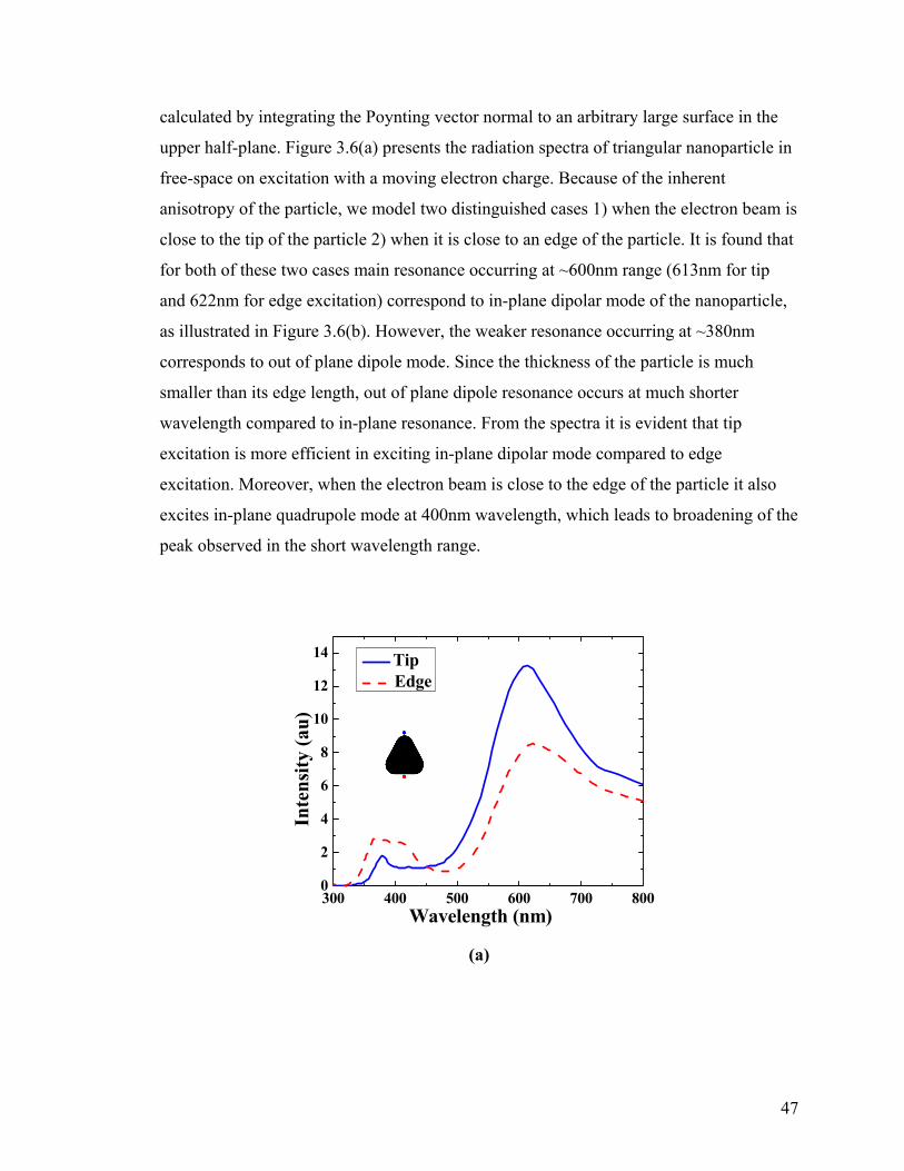
47
calculated by integrating the Poynting vector normal to an arbitrary large surface in the
upper half-plane. Figure 3.6(a) presents the radiation spectra of triangular nanoparticle in
free-space on excitation with a moving electron charge. Because of the inherent
anisotropy of the particle, we model two distinguished cases 1) when the electron beam is
close to the tip of the particle 2) when it is close to an edge of the particle. It is found that
for both of these two cases main resonance occurring at ~600nm range (613nm for tip
and 622nm for edge excitation) correspond to in-plane dipolar mode of the nanoparticle,
as illustrated in Figure 3.6(b). However, the weaker resonance occurring at ~380nm
corresponds to out of plane dipole mode. Since the thickness of the particle is much
smaller than its edge length, out of plane dipole resonance occurs at much shorter
wavelength compared to in-plane resonance. From the spectra it is evident that tip
excitation is more efficient in exciting in-plane dipolar mode compared to edge
excitation. Moreover, when the electron beam is close to the edge of the particle it also
excites in-plane quadrupole mode at 400nm wavelength, which leads to broadening of the
peak observed in the short wavelength range.
300 400 500 600 700 8000
2
4
6
8
10
12
14
Inte
nsity
(au)
Wavelength (nm)
Tip Edge
(a)
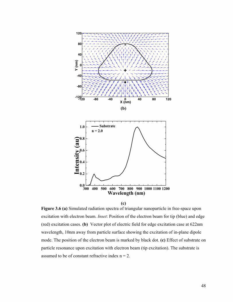
48
-120 -80 -40 0 40 80 120-120
-80
-40
0
40
80
120
X (nm)
Y (
nm
)
+
-
(b)
300 400 500 600 700 800 900 1000 1100 12000.0
0.2
0.4
0.6
0.8
1.0
Inte
nsity
(au)
Wavelength (nm)
Substraten = 2.0
(c)
Figure 3.6 (a) Simulated radiation spectra of triangular nanoparticle in free-space upon
excitation with electron beam. Inset: Position of the electron beam for tip (blue) and edge
(red) excitation cases. (b) Vector plot of electric field for edge excitation case at 622nm
wavelength, 10nm away from particle surface showing the excitation of in-plane dipole
mode. The position of the electron beam is marked by black dot. (c) Effect of substrate on
particle resonance upon excitation with electron beam (tip excitation). The substrate is
assumed to be of constant refractive index n = 2.
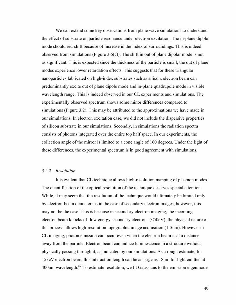
49
We can extend some key observations from plane wave simulations to understand
the effect of substrate on particle resonance under electron excitation. The in-plane dipole
mode should red-shift because of increase in the index of surroundings. This is indeed
observed from simulations (Figure 3.6(c)). The shift in out of plane dipolar mode is not
as significant. This is expected since the thickness of the particle is small, the out of plane
modes experience lower retardation effects. This suggests that for these triangular
nanoparticles fabricated on high-index substrates such as silicon, electron beam can
predominantly excite out of plane dipole mode and in-plane quadrupole mode in visible
wavelength range. This is indeed observed in our CL experiments and simulations. The
experimentally observed spectrum shows some minor differences compared to
simulations (Figure 3.2). This may be attributed to the approximations we have made in
our simulations. In electron excitation case, we did not include the dispersive properties
of silicon substrate in our simulations. Secondly, in simulations the radiation spectra
consists of photons integrated over the entire top half space. In our experiments, the
collection angle of the mirror is limited to a cone angle of 160 degrees. Under the light of
these differences, the experimental spectrum is in good agreement with simulations.
3.2.2 Resolution
It is evident that CL technique allows high-resolution mapping of plasmon modes.
The quantification of the optical resolution of the technique deserves special attention.
While, it may seem that the resolution of the technique would ultimately be limited only
by electron-beam diameter, as in the case of secondary electron images, however, this
may not be the case. This is because in secondary electron imaging, the incoming
electron beam knocks off low energy secondary electrons (<50eV); the physical nature of
this process allows high-resolution topographic image acquisition (1-5nm). However in
CL imaging, photon emission can occur even when the electron beam is at a distance
away from the particle. Electron beam can induce luminescence in a structure without
physically passing through it, as indicated by our simulations. As a rough estimate, for
15keV electron beam, this interaction length can be as large as 18nm for light emitted at
400nm wavelength.52 To estimate resolution, we fit Gaussians to the emission eigenmode
50
at 400nm wavelength. A clear spatial modulation (25% change in normalized intensity)
of the eigenmode above the noise level is detectable on length scale as short as 25nm.
This is illustrated in Figure 3.7, which plots the variation of radiation intensity along the
edge of the particle as marked in Figure 3.4(a).
0 50 100 150 2000
10
20
30
40
50
60
70
Inte
nsity
(au)
X (nm)
25nm
Figure 3.7 Variation of cathodoluminescence emission along the edge of the particle
(marked in Figure 3.4(a)) at 400nm wavelength.
3.3 Summary
In this work CL imaging technique was utilized to image plasmon modes of Ag
triangular nanoparticles with high-spatial (~25nm) and spectral resolution (~5.4nm).
Spectroscopic analysis when combined with monochromatic imaging helps us to identify
different channels of emission of plasmon modes. The process of radiative emission of
plasmon modes in CL setup was modeled using FDTD approach. Simulations indicate
that in contrast to light excitation, electron beam not only excites the in-plane eigenmodes
of nanoparticles but is also able to excite out of plane modes. Because of the inherent
anisotropy of the triangular particle, the position of the electron beam also influences the
excitation of eigenmodes. This was presented in the context of “tip” and “edge”
excitation of the particle. These results provide a better understanding of excitation and
imaging of plasmon modes using CL spectroscopy.
51
Methods
Fabrication:
For the purpose of this study, Ag nanostructures were fabricated on silicon
substrate. The samples were fabricated using a novel solid-state superionic stamping (S4)
process.2, 70 This process utilizes a pre-patterned stamp made of a superionic conductor
such as silver sulfide which supports a mobile cation (silver). The stamp is brought into
contact with a substrate coated with a thin silver film. On the application of an electrical
bias with the substrate as anode and a metallic electrode at the back of the stamp as
cathode, a solid state electrochemical reaction takes place only at the actual contact at the
interface. This reaction progressively removes a metallic layer of the substrate at the
contact area with the stamp. Assisted by a nominal pressure to maintain electrical contact,
the stamp gradually progresses into the substrate, generating a pattern in the silver film
complementary to the pre-patterned features on the stamp. Silver sulfide stamps were
patterned using focused ion beam technique. A very thin (~2nm) chromium (Cr) layer is
used as the adhesion layer for silver film on silicon. The fabricated structures are coated
conformally with very thin dielectric layer (anatase TiO2, 5 monolayer ~ 2.5Å) using
atomic layer deposition (ALD) to protect the samples from environmental and electron
beam damage. Excellent pattern transfer fidelity of the S4 approach down to sub-50nm
resolution and ambient operating conditions make this process suitable for low-cost,
high-throughput patterning of plasmonic nanostructures, such as presented in this study.
Simulation:
Light excitation: To numerically compute absorption and scattering by triangular
nanoparticles, we utilize the total-field scattered-field (TFSF) formulation with FDTD
approach. In this approach, the computation region is divided into two sections – one
where the total field (incident + scattered) is computed and the second where only
scattered field is computed. The particles are excited by a normal incident plane wave.
Absorption and scattering cross-section are computed by monitoring the net power inflow
in the total-field region near the particle and net power outflow in the scattered field
region, respectively. Extinction cross-section is the sum of absorption and scattering

52
cross-section of the particle. Our numerical calculations suggest that for Ag nanoparticles
scattering is approximately an order of magnitude larger than absorption. The material
properties used in the calculation are obtained from generalized multi-coefficient model40
that fits the dispersion data obtained from Palik71. This approach is more accurate for
broadband simulations than fitting a single material model such as Drude or Lorentz.
Electron excitation: The electron beam has been modeled as a series of closely
spaced dipoles each with temporal phase delay according to the velocity of the electron
beam. In the absence of any structure, electron beam moving at a constant velocity does
not generate any radiation. In FDTD, however, we simulate only a finite portion of the
electron path and the sudden appearance and disappearance of the electron will generate
radiation. To solve this problem, we run a second, reference simulation where all the
structures are removed, and we can calculate the electromagnetic fields at any
wavelength by taking the difference in fields between the simulations.40 To get an
accurate difference, we force the simulation mesh to be exactly the same with and
without the structure. Currently, the methodology doesn’t permit electron beam to pass
through a lossy or dispersive substrate material.
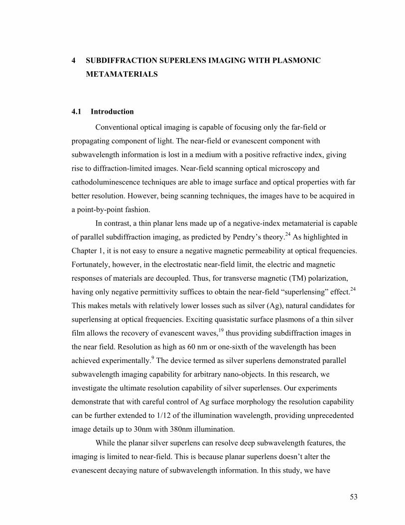
53
4 SUBDIFFRACTION SUPERLENS IMAGING WITH PLASMONIC
METAMATERIALS
4.1 Introduction
Conventional optical imaging is capable of focusing only the far-field or
propagating component of light. The near-field or evanescent component with
subwavelength information is lost in a medium with a positive refractive index, giving
rise to diffraction-limited images. Near-field scanning optical microscopy and
cathodoluminescence techniques are able to image surface and optical properties with far
better resolution. However, being scanning techniques, the images have to be acquired in
a point-by-point fashion.
In contrast, a thin planar lens made up of a negative-index metamaterial is capable
of parallel subdiffraction imaging, as predicted by Pendry’s theory.24 As highlighted in
Chapter 1, it is not easy to ensure a negative magnetic permeability at optical frequencies.
Fortunately, however, in the electrostatic near-field limit, the electric and magnetic
responses of materials are decoupled. Thus, for transverse magnetic (TM) polarization,
having only negative permittivity suffices to obtain the near-field “superlensing” effect.24
This makes metals with relatively lower losses such as silver (Ag), natural candidates for
superlensing at optical frequencies. Exciting quasistatic surface plasmons of a thin silver
film allows the recovery of evanescent waves,19 thus providing subdiffraction images in
the near field. Resolution as high as 60 nm or one-sixth of the wavelength has been
achieved experimentally.9 The device termed as silver superlens demonstrated parallel
subwavelength imaging capability for arbitrary nano-objects. In this research, we
investigate the ultimate resolution capability of silver superlenses. Our experiments
demonstrate that with careful control of Ag surface morphology the resolution capability
can be further extended to 1/12 of the illumination wavelength, providing unprecedented
image details up to 30nm with 380nm illumination.
While the planar silver superlens can resolve deep subwavelength features, the
imaging is limited to near-field. This is because planar superlens doesn’t alter the
evanescent decaying nature of subwavelength information. In this study, we have
54
investigated a far-field superlens operating at near-infrared (IR) wavelengths that allows
resolving subwavelength features in the far-field. By utilizing evanescent enhancement
provided by plasmonic materials such as silver nanorods and Moiré effect, we
numerically demonstrate that subwavelength information of an object can be converted to
far-field or propagating information which in turn, can be captured by conventional
optical components. A simple image restoration algorithm can then be used to reconstruct
the object with subwavelength resolution.
This unique class of optical superlenses with potential molecular scale resolution
capability will enable parallel imaging (illustration Figure 4.1) and nanofabrication in a
single snapshot, a feat that is not yet available with other nanoscale imaging and
fabrication techniques such as atomic force microscopy and electron beam lithography.
Figure 4.1 Realization of high-resolution superlens would open up the possibility of
novel applications, such as imaging of biomolecules in their natural environment.72
4.2 Smooth superlens
Theoretically, silver superlens is capable of λ/20- λ/30 image resolution (where λ
is incident wavelength).25, 26 However, challenges remain to realize such a high resolution
imaging system, such as minimizing the information loss due to evanescent decay,
absorption or scattering. Our calculations (not presented here) have indicated that the
55
thickness of spacer layer (separating the object and the lens) and that of silver film are the
two major governing factors that determine subwavelength information loss due to
evanescent decay and material absorption. Particularly, the surface morphology of silver
film plays a significant role in determining the image resolution capability. Below a
critical thickness silver is known to form rough islandized films.27 Rougher films perturb
the surface plasmon modes causing loss of subwavelength details and hence diminished
resolution.73 Producing thin, uniform, and ultra-smooth silver films has been a holy-grail
for plasmonics, molecular electronics and nanophotonics.
Recent research efforts directed toward smoothing thin silver films have resulted
in novel approaches capable of producing ultrathin silver films with atomic-scale
roughness. Logeeswaran et al. demonstrated that simple mechanical pressure can
generate smooth films by flattening bumps, asperities, and rough grains of a freshly
vacuum-deposited metal film.74 The authors demonstrated that mechanical pressing of
100nm films at ~600MPa can reduce the root-mean square (RMS) roughness from 13nm
to 0.1nm. However, the technique suffers from issues common to contact processes such
as creation of surface defects, scratches, and delamination of silver films.
In this work, we explore a new approach to grow ultra-smooth silver films
characterized by much smaller RMS surface roughness. An intermediate ultra-thin
germanium (Ge) layer (~1nm) is introduced before depositing Ag. Utilizing Ag-Ge
surface interactions, smooth superlens down to 15nm Ag thickness has been fabricated. It
is observed that introducing the Ge layer drastically improves Ag surface morphology
and helps minimize the island cluster formation. Roughness measurements of thin silver
films (15nm) deposited with and without Ge layer (1nm) were performed using atomic
force microscopy (AFM) and X-ray reflectivity (XRR) techniques. AFM measurements
directly reveal the surface topography and it is observed that the RMS roughness of Ag
(over 1x1µm scan area) deposited on quartz substrate improves from 2.7nm down to
0.8nm by introducing Ge (Figure 4.2(a), (b)). In XRR measurements, the decay in overall
reflected intensity and the oscillation amplitude is strongly affected by the roughness of
films. These measurements also suggest drastic improvements in the quality of Ag films
incorporating Ge (Figure 4.2(c)). Intensity reflected from sample 1 (without Ge - blue
dotted curve) drops sharply and does not show oscillating fringes owing to large
56
roughness of the Ag film. In contrast, sample 2 (with Ge – black solid curve) shows large
number of fringes and a slow decay in intensity suggesting highly uniform films.
Experimental data fit (red dashed curve) reveals that the roughness of 15nm thick Ag film
in sample 2 is <0.58nm, more than 4 times smoother compared to sample 1. This is
attributed to the fact that surface diffusion of Ag on glass (SiO2) is energetically
favorable compared to diffusion on Ge.75 Hence, Ge acts as a wetting layer for Ag and
helps a layer by layer growth.
(a)
(b)

57
0.5 1.0 1.5 2.0 2.5100
101
102
103
104
105
106
Inte
nsity
(cps
)
Incident angle (Deg)
Ag/Ge Ag/Ge (Fit) Ag
(c)
Figure 4.2 Smooth Ag growth on Ge (a) Surface topology from AFM micrographs
(1x1µm scan) 15nm Ag deposited on quartz substrate and (b) 15nm Ag deposited with
1nm Ge on quartz substrate. (c) XRR studies of thin Ag films grown directly on quartz
and with Ge intermediate layer.
The configuration of the smooth silver superlens is illustrated in Figure 4.3. An
array of chrome (Cr) gratings 40nm thick with 30nm half-pitch, which serve as the
object, was patterned using a nanoimprint process (see methods). In Figure 4.4, we
present a step-by-step surface characterization of the prepared smooth silver superlens
with embedded chrome gratings using AFM. In order to prepare a flat superlens on top of
the objects (Figure 4.4(a)), it is necessary to deposit a planarization layer to reduce the
surface modulations. Surface modulations can alter the dispersion characteristics of the
plasmons and it smears out the image details. Also, the planarization layer should be thin
to prevent a significant loss of evanescent components from the object. In our process, a
planarization procedure using nanoimprint technique is developed to reduce the surface
modulations below 1.3 nm (Figure 4.4(b)). This is achieved by flood-exposure of 66nm
thick UV spacer layer over a flat quartz window under pressure, followed by subsequent
reactive ion etching (RIE) to back etch the spacer to 6nm thickness on top of the chrome
gratings. A 35nm thick Cr window layer is photolithographically patterned on top of the
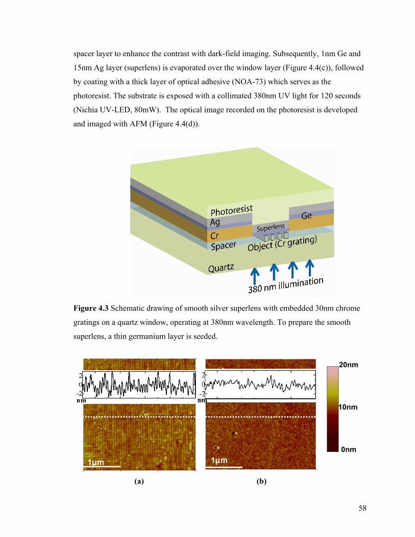
58
spacer layer to enhance the contrast with dark-field imaging. Subsequently, 1nm Ge and
15nm Ag layer (superlens) is evaporated over the window layer (Figure 4.4(c)), followed
by coating with a thick layer of optical adhesive (NOA-73) which serves as the
photoresist. The substrate is exposed with a collimated 380nm UV light for 120 seconds
(Nichia UV-LED, 80mW). The optical image recorded on the photoresist is developed
and imaged with AFM (Figure 4.4(d)).
Figure 4.3 Schematic drawing of smooth silver superlens with embedded 30nm chrome
gratings on a quartz window, operating at 380nm wavelength. To prepare the smooth
superlens, a thin germanium layer is seeded.
(a) (b)
0nm
10nm
20nm
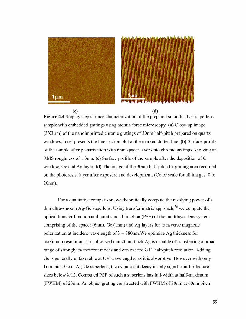
59
(c) (d) Figure 4.4 Step by step surface characterization of the prepared smooth silver superlens
sample with embedded gratings using atomic force microscopy. (a) Close-up image
(3X3µm) of the nanoimprinted chrome gratings of 30nm half-pitch prepared on quartz
windows. Inset presents the line section plot at the marked dotted line. (b) Surface profile
of the sample after planarization with 6nm spacer layer onto chrome gratings, showing an
RMS roughness of 1.3nm. (c) Surface profile of the sample after the deposition of Cr
window, Ge and Ag layer. (d) The image of the 30nm half-pitch Cr grating area recorded
on the photoresist layer after exposure and development. (Color scale for all images: 0 to
20nm).
For a qualitative comparison, we theoretically compute the resolving power of a
thin ultra-smooth Ag-Ge superlens. Using transfer matrix approach,76 we compute the
optical transfer function and point spread function (PSF) of the multilayer lens system
comprising of the spacer (6nm), Ge (1nm) and Ag layers for transverse magnetic
polarization at incident wavelength of λ = 380nm.We optimize Ag thickness for
maximum resolution. It is observed that 20nm thick Ag is capable of transferring a broad
range of strongly evanescent modes and can exceed λ/11 half-pitch resolution. Adding
Ge is generally unfavorable at UV wavelengths, as it is absorptive. However with only
1nm thick Ge in Ag-Ge superlens, the evanescent decay is only significant for feature
sizes below λ/12. Computed PSF of such a superlens has full-width at half-maximum
(FWHM) of 23nm. An object grating constructed with FWHM of 30nm at 60nm pitch
1µm1µm
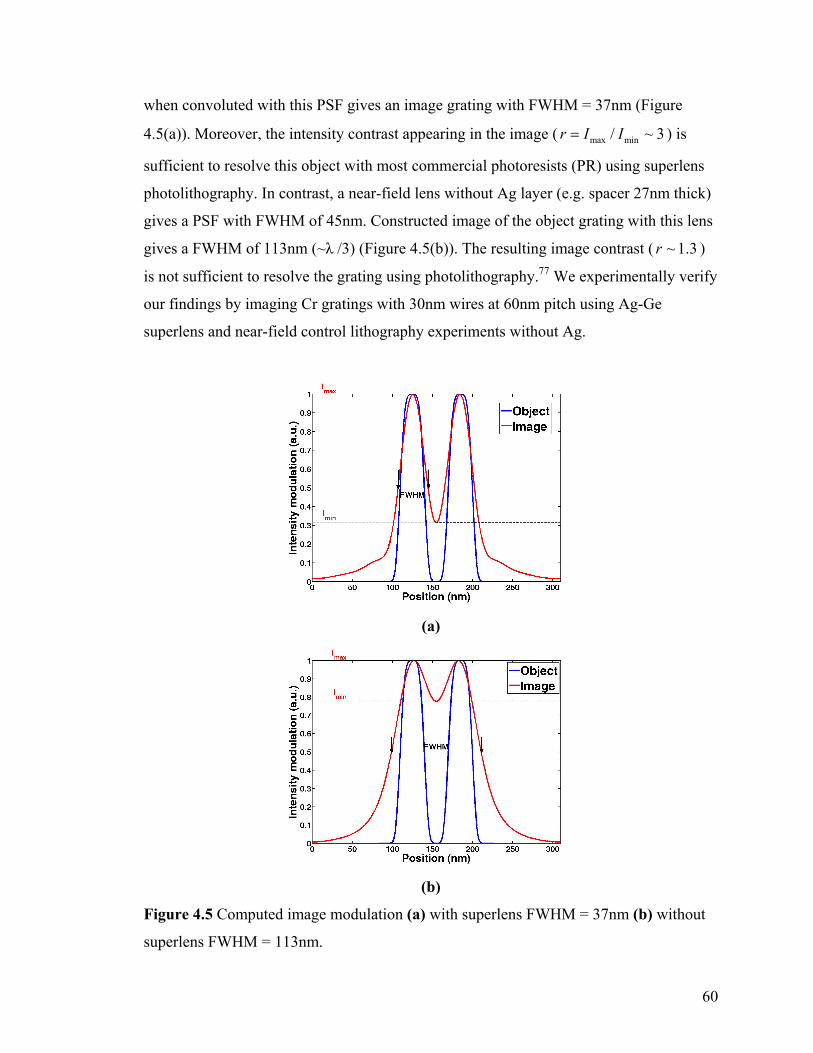
60
when convoluted with this PSF gives an image grating with FWHM = 37nm (Figure
4.5(a)). Moreover, the intensity contrast appearing in the image ( max min/ ~ 3r I I= ) is
sufficient to resolve this object with most commercial photoresists (PR) using superlens
photolithography. In contrast, a near-field lens without Ag layer (e.g. spacer 27nm thick)
gives a PSF with FWHM of 45nm. Constructed image of the object grating with this lens
gives a FWHM of 113nm (~λ /3) (Figure 4.5(b)). The resulting image contrast ( ~ 1.3r )
is not sufficient to resolve the grating using photolithography.77 We experimentally verify
our findings by imaging Cr gratings with 30nm wires at 60nm pitch using Ag-Ge
superlens and near-field control lithography experiments without Ag.
(a)
(b)
Figure 4.5 Computed image modulation (a) with superlens FWHM = 37nm (b) without
superlens FWHM = 113nm.
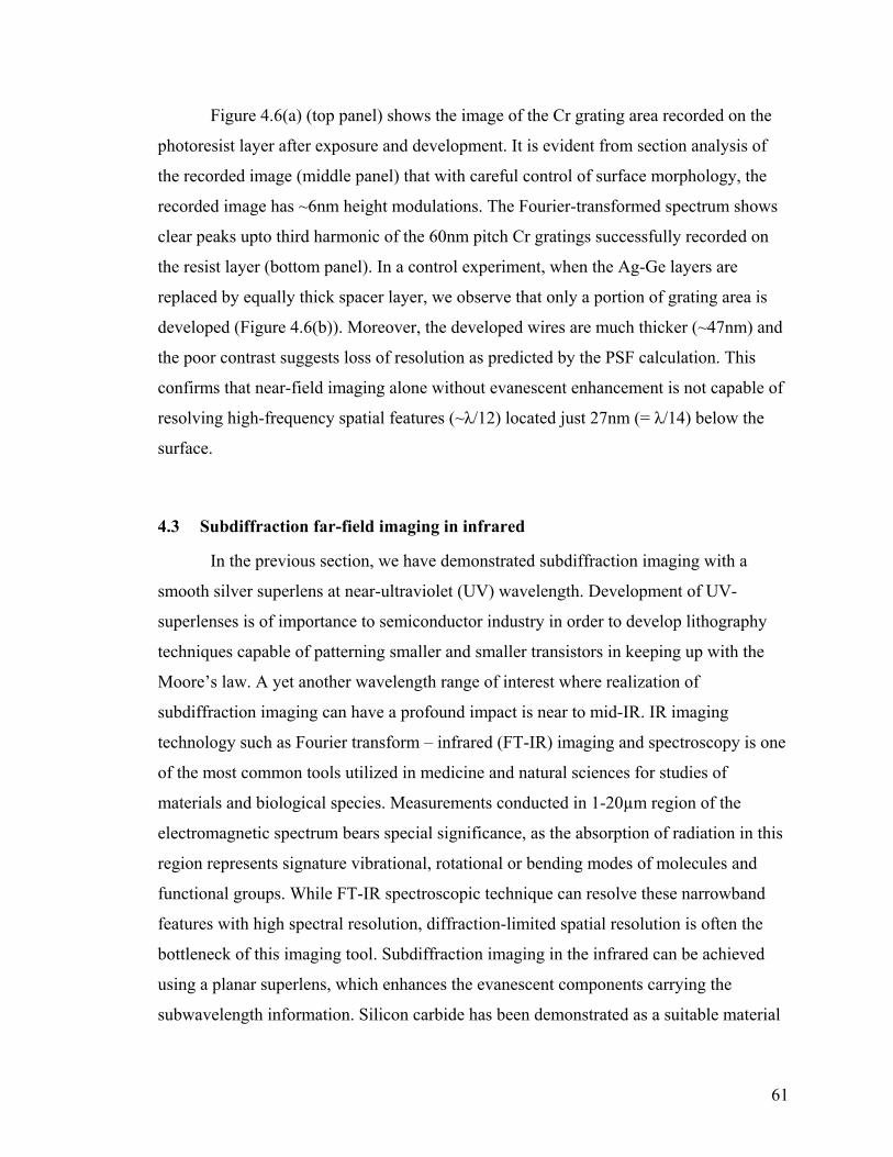
61
Figure 4.6(a) (top panel) shows the image of the Cr grating area recorded on the
photoresist layer after exposure and development. It is evident from section analysis of
the recorded image (middle panel) that with careful control of surface morphology, the
recorded image has ~6nm height modulations. The Fourier-transformed spectrum shows
clear peaks upto third harmonic of the 60nm pitch Cr gratings successfully recorded on
the resist layer (bottom panel). In a control experiment, when the Ag-Ge layers are
replaced by equally thick spacer layer, we observe that only a portion of grating area is
developed (Figure 4.6(b)). Moreover, the developed wires are much thicker (~47nm) and
the poor contrast suggests loss of resolution as predicted by the PSF calculation. This
confirms that near-field imaging alone without evanescent enhancement is not capable of
resolving high-frequency spatial features (~λ/12) located just 27nm (= λ/14) below the
surface.
4.3 Subdiffraction far-field imaging in infrared
In the previous section, we have demonstrated subdiffraction imaging with a
smooth silver superlens at near-ultraviolet (UV) wavelength. Development of UV-
superlenses is of importance to semiconductor industry in order to develop lithography
techniques capable of patterning smaller and smaller transistors in keeping up with the
Moore’s law. A yet another wavelength range of interest where realization of
subdiffraction imaging can have a profound impact is near to mid-IR. IR imaging
technology such as Fourier transform – infrared (FT-IR) imaging and spectroscopy is one
of the most common tools utilized in medicine and natural sciences for studies of
materials and biological species. Measurements conducted in 1-20µm region of the
electromagnetic spectrum bears special significance, as the absorption of radiation in this
region represents signature vibrational, rotational or bending modes of molecules and
functional groups. While FT-IR spectroscopic technique can resolve these narrowband
features with high spectral resolution, diffraction-limited spatial resolution is often the
bottleneck of this imaging tool. Subdiffraction imaging in the infrared can be achieved
using a planar superlens, which enhances the evanescent components carrying the
subwavelength information. Silicon carbide has been demonstrated as a suitable material
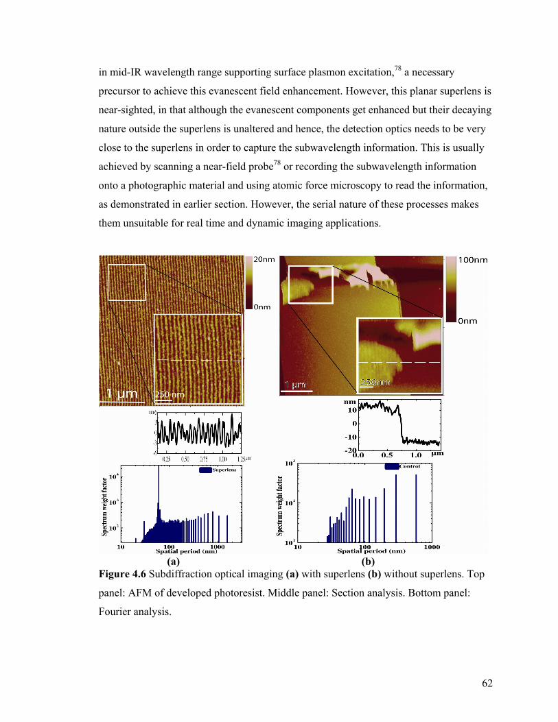
62
in mid-IR wavelength range supporting surface plasmon excitation,78 a necessary
precursor to achieve this evanescent field enhancement. However, this planar superlens is
near-sighted, in that although the evanescent components get enhanced but their decaying
nature outside the superlens is unaltered and hence, the detection optics needs to be very
close to the superlens in order to capture the subwavelength information. This is usually
achieved by scanning a near-field probe78 or recording the subwavelength information
onto a photographic material and using atomic force microscopy to read the information,
as demonstrated in earlier section. However, the serial nature of these processes makes
them unsuitable for real time and dynamic imaging applications.
(a) (b)
Figure 4.6 Subdiffraction optical imaging (a) with superlens (b) without superlens. Top
panel: AFM of developed photoresist. Middle panel: Section analysis. Bottom panel:
Fourier analysis.
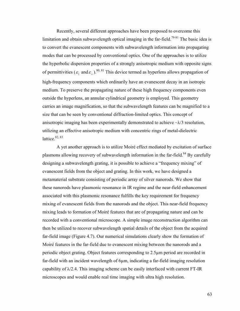
63
Recently, several different approaches have been proposed to overcome this
limitation and obtain subwavelength optical imaging in the far-field.79-81 The basic idea is
to convert the evanescent components with subwavelength information into propagating
modes that can be processed by conventional optics. One of the approaches is to utilize
the hyperbolic dispersion properties of a strongly anisotropic medium with opposite signs
of permittivities ( ||ε andε⊥ ).80, 81 This device termed as hyperlens allows propagation of
high-frequency components which ordinarily have an evanescent decay in an isotropic
medium. To preserve the propagating nature of these high frequency components even
outside the hyperlens, an annular cylindrical geometry is employed. This geometry
carries an image magnification, so that the subwavelength features can be magnified to a
size that can be seen by conventional diffraction-limited optics. This concept of
anisotropic imaging has been experimentally demonstrated to achieve ~λ/3 resolution,
utilizing an effective anisotropic medium with concentric rings of metal-dielectric
lattice.82, 83
A yet another approach is to utilize Moiré effect mediated by excitation of surface
plasmons allowing recovery of subwavelength information in the far-field.84 By carefully
designing a subwavelength grating, it is possible to achieve a “frequency mixing” of
evanescent fields from the object and grating. In this work, we have designed a
metamaterial substrate consisting of periodic array of silver nanorods. We show that
these nanorods have plasmonic resonance in IR regime and the near-field enhancement
associated with this plasmonic resonance fulfills the key requirement for frequency
mixing of evanescent fields from the nanorods and the object. This near-field frequency
mixing leads to formation of Moiré features that are of propagating nature and can be
recorded with a conventional microscope. A simple image reconstruction algorithm can
then be utilized to recover subwavelength spatial details of the object from the acquired
far-field image (Figure 4.7). Our numerical simulations clearly show the formation of
Moiré features in the far-field due to evanescent mixing between the nanorods and a
periodic object grating. Object features corresponding to 2.5µm period are recorded in
far-field with an incident wavelength of 6µm, indicating a far-field imaging resolution
capability of λ/2.4. This imaging scheme can be easily interfaced with current FT-IR
microscopes and would enable real time imaging with ultra high resolution.
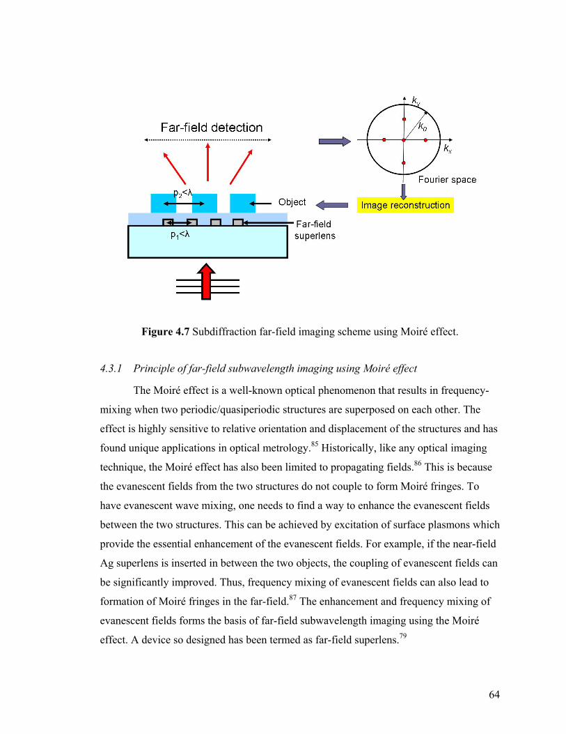
64
Figure 4.7 Subdiffraction far-field imaging scheme using Moiré effect.
4.3.1 Principle of far-field subwavelength imaging using Moiré effect
The Moiré effect is a well-known optical phenomenon that results in frequency-
mixing when two periodic/quasiperiodic structures are superposed on each other. The
effect is highly sensitive to relative orientation and displacement of the structures and has
found unique applications in optical metrology.85 Historically, like any optical imaging
technique, the Moiré effect has also been limited to propagating fields.86 This is because
the evanescent fields from the two structures do not couple to form Moiré fringes. To
have evanescent wave mixing, one needs to find a way to enhance the evanescent fields
between the two structures. This can be achieved by excitation of surface plasmons which
provide the essential enhancement of the evanescent fields. For example, if the near-field
Ag superlens is inserted in between the two objects, the coupling of evanescent fields can
be significantly improved. Thus, frequency mixing of evanescent fields can also lead to
formation of Moiré fringes in the far-field.87 The enhancement and frequency mixing of
evanescent fields forms the basis of far-field subwavelength imaging using the Moiré
effect. A device so designed has been termed as far-field superlens.79
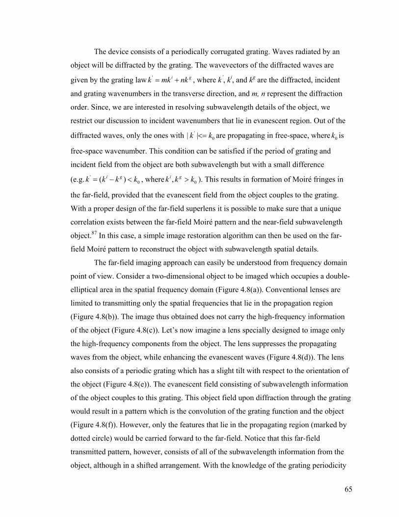
65
The device consists of a periodically corrugated grating. Waves radiated by an
object will be diffracted by the grating. The wavevectors of the diffracted waves are
given by the grating law ' i gk mk nk= + , where k’, ki, and kg are the diffracted, incident
and grating wavenumbers in the transverse direction, and m, n represent the diffraction
order. Since, we are interested in resolving subwavelength details of the object, we
restrict our discussion to incident wavenumbers that lie in evanescent region. Out of the
diffracted waves, only the ones with '0| |k k<= are propagating in free-space, where 0k is
free-space wavenumber. This condition can be satisfied if the period of grating and
incident field from the object are both subwavelength but with a small difference
(e.g. '0( )i gk k k k= − < , where 0,i gk k k> ). This results in formation of Moiré fringes in
the far-field, provided that the evanescent field from the object couples to the grating.
With a proper design of the far-field superlens it is possible to make sure that a unique
correlation exists between the far-field Moiré pattern and the near-field subwavelength
object.87 In this case, a simple image restoration algorithm can then be used on the far-
field Moiré pattern to reconstruct the object with subwavelength spatial details.
The far-field imaging approach can easily be understood from frequency domain
point of view. Consider a two-dimensional object to be imaged which occupies a double-
elliptical area in the spatial frequency domain (Figure 4.8(a)). Conventional lenses are
limited to transmitting only the spatial frequencies that lie in the propagation region
(Figure 4.8(b)). The image thus obtained does not carry the high-frequency information
of the object (Figure 4.8(c)). Let’s now imagine a lens specially designed to image only
the high-frequency components from the object. The lens suppresses the propagating
waves from the object, while enhancing the evanescent waves (Figure 4.8(d)). The lens
also consists of a periodic grating which has a slight tilt with respect to the orientation of
the object (Figure 4.8(e)). The evanescent field consisting of subwavelength information
of the object couples to this grating. This object field upon diffraction through the grating
would result in a pattern which is the convolution of the grating function and the object
(Figure 4.8(f)). However, only the features that lie in the propagating region (marked by
dotted circle) would be carried forward to the far-field. Notice that this far-field
transmitted pattern, however, consists of all of the subwavelength information from the
object, although in a shifted arrangement. With the knowledge of the grating periodicity
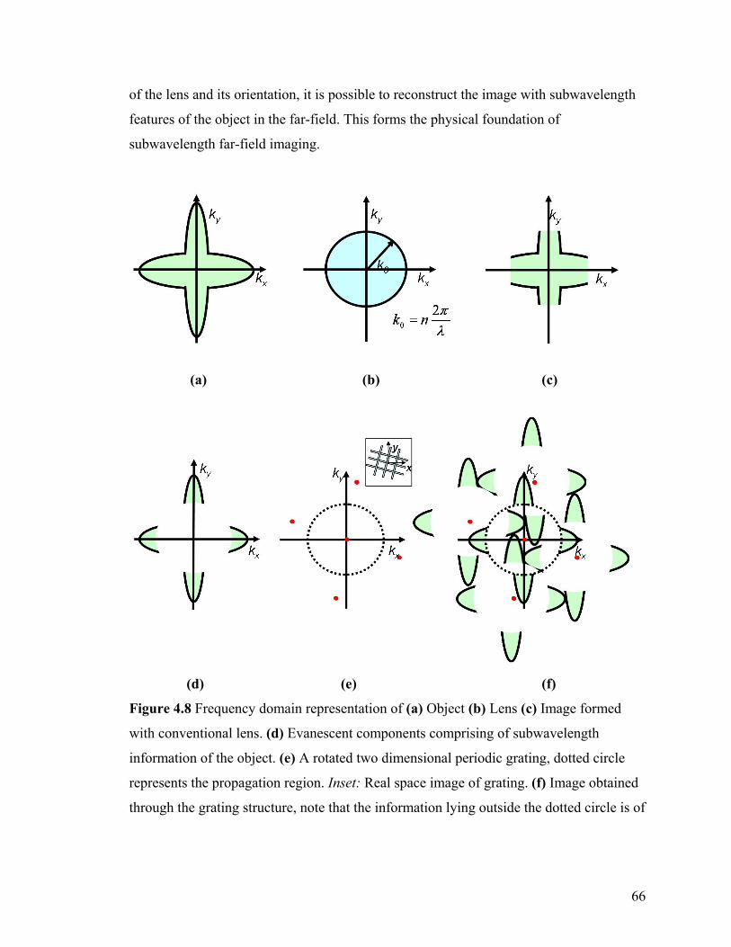
66
of the lens and its orientation, it is possible to reconstruct the image with subwavelength
features of the object in the far-field. This forms the physical foundation of
subwavelength far-field imaging.
(a) (b) (c)
(d) (e) (f)
Figure 4.8 Frequency domain representation of (a) Object (b) Lens (c) Image formed
with conventional lens. (d) Evanescent components comprising of subwavelength
information of the object. (e) A rotated two dimensional periodic grating, dotted circle
represents the propagation region. Inset: Real space image of grating. (f) Image obtained
through the grating structure, note that the information lying outside the dotted circle is of
67
decaying nature, and only the information within the dotted circle is carried forward to
the far-field.
4.3.2 Design of far-field superlens in infrared
As mentioned above, a key requirement to achieve Moiré effect for evanescent
fields is to ensure field enhancement and coupling between the object and the lens.
Surface plasmons provide the essential route to achieve this. However, direct excitation
of surface plasmons on a planar interface between metal and dielectric in the infrared
regime is limited by the choice of appropriate materials. To address this challenge, we
note that the use of discrete plasmonic elements can achieve both goals; first to enhance
near-field coupling with the object and second to transform the near-field components to
far-field in the form of Moiré features. In this study, we have designed a metamaterial
substrate consisting of discrete elements that provide surface plasmon excitation in IR.
The metamaterial substrate consists of two-dimensional array of Ag nanorods. These
nanorods support plasmonic resonance in IR range.88 The fundamental dipolar resonance
of the nanorods (with dimensions 1000 x 200 x 200 nm) on silicon substrate (mid-IR
transparent) is observed at a wavelength of λ = 6.1µm. This matches reasonably well with
the classical description from antenna theory, which predicts the dipolar resonance
at 2 5.04res nL mλ μ= = , where n is the effective refractive index of the surroundings and
L is the length of linear antenna. Substrate effect can be taken into account by taking an
average permittivity of the surroundings. Deviation of the resonance wavelength from
antenna theory is attributed to the finite penetration of the electromagnetic field into
nanorods (non-zero skin depth) and periodic arrangement of the rods. Since, the cross-
section dimension of the nanorod is much smaller than wavelength but larger than the
skin depth of metal, the resonance and linewidth are found out to be almost independent
of it. The nanorod resonance is strongly polarization dependent and is observed only
when the electric field is aligned parallel to the rod axis. Figure 4.9(a) presents the
normal incidence far-field transmission spectra of periodic array of nanorods (lattice
2x2µm). At resonance, nanorods exhibit strong extinction due to excitation of surface
plasmons.
68
3 4 5 6 7 8 9 10
0.62
0.64
0.66
0.68
0.70
0.72
Tra
nsm
ittan
ce
Wavelength (μm)
Perpendicular polarization Parallel polarization
1μm
(a)
X (μm)
Y (μ m
)
-3 -2 -1 0 1 2 3
-3
-2
-1
0
1
2
3
10
20
30
40
50
60
70
80
(b)
Figure 4.9 (a) Transmission spectra of periodic array of Ag nanorods in the IR region.
Resonance is observed only for parallel polarization, i.e. when the electric field is aligned
along the direction of rod axis. (b) Near-field intensity calculated 20nm above the surface
of the rods at the fundamental dipolar resonance λ = 6.1µm.
Calculated near-field intensity (~20nm above the surface of the nanorods) show
local-field enhancement at the fundamental dipolar resonance (Figure 4.9(b)). In a
separate study by Neubrech et al.,89 this near-field enhancement has been shown to
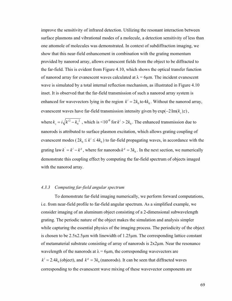
69
improve the sensitivity of infrared detection. Utilizing the resonant interaction between
surface plasmons and vibrational modes of a molecule, a detection sensitivity of less than
one attomole of molecules was demonstrated. In context of subdiffraction imaging, we
show that this near-field enhancement in combination with the grating momentum
provided by nanorod array, allows evanescent fields from the object to be diffracted to
the far-field. This is evident from Figure 4.10, which shows the optical transfer function
of nanorod array for evanescent waves calculated at λ = 6µm. The incident evanescent
wave is simulated by a total internal reflection mechanism, as illustrated in Figure 4.10
inset. It is observed that the far-field transmission of such a nanorod array system is
enhanced for wavevectors lying in the region 02ik k= to 04k . Without the nanorod array,
evanescent waves have far-field transmission intensity given by exp( 2 Im( ) )zk z− ,
where 2 20
izk i k k= − , which is <10-9 for 02ik k> . The enhanced transmission due to
nanorods is attributed to surface plasmon excitation, which allows grating coupling of
evanescent modes ( 0 02 4ik k k≤ ≤ ) to far-field propagating waves, in accordance with the
grating law ' i gk k k= − , where for nanorods 03gk k= . In the next section, we numerically
demonstrate this coupling effect by computing the far-field spectrum of objects imaged
with the nanorod array.
4.3.3 Computing far-field angular spectrum
To demonstrate far-field imaging numerically, we perform forward computations,
i.e. from near-field profile to far-field angular spectrum. As a simplified example, we
consider imaging of an aluminum object consisting of a 2-dimensional subwavelength
grating. The periodic nature of the object makes the simulation and analysis simpler
while capturing the essential physics of the imaging process. The periodicity of the object
is chosen to be 2.5x2.5µm with linewidth of 1.25µm. The corresponding lattice constant
of metamaterial substrate consisting of array of nanorods is 2x2µm. Near the resonance
wavelength of the nanorods at λ = 6µm, the corresponding wavevectors are
02.4ik k= (object), and 03gk k= (nanorods). It can be seen that diffracted waves
corresponding to the evanescent wave mixing of these wavevector components are
70
propagating only through first order diffraction '0( ) 0.6i gk k k k= − = . Hence, there is no
overlap between diffracted waves and a clear one to one relationship exists between far-
field angular spectrum and near-field object profile.
2.0 2.5 3.0 3.5 4.0 4.5 5.00
2
4
6T
rans
mis
sion
(far
-fie
ld)
ki/k0
Nanorod transfer function Parallel polarization Perpendicular polarization
x10-3
Figure 4.10 Far-field transmission computed for various incident transverse
wavenumbers at λ = 6µm, for parallel and perpendicular polarization. Inset: Schematic of
the simulation geometry. A total internal reflection mechanism is utilized to simulate
evanescent wave incidence on the nanorod array.
To obtain the far-field angular spectrum, we utilize the fact that in the far-field
only contribution to a point of observation is from a plane wave originating from the
source and propagating along the radial direction to the point of observation. We have
performed numerical simulations to compute the far-field angular spectrum of nanorods
overlapped with a subwavelength object grating. Simulations are performed using a
commercial finite-difference time-domain tool.40 The nanorods on silicon substrate are
physically separated from the subwavelength object grating by a thin (50nm) dielectric
50nm
1µm
0 0sinxk nk kθ= >
2µm
λ = 6µm θ
71
spacer layer. A plane wave illumination is assumed from the substrate side and near-field
profile is monitored 50nm away from the subwavelength object on the air side. Periodic
boundary conditions are assumed in x-y directions with a period of 10µm, which is
integral multiple of the period of the rods and the object. The near-field data (Ex, Ey, Ez)
recorded in the simulations is decomposed into plane waves using a far-field projection
algorithm which gives the far-field angular spectrum of the field on the surface of a
sphere (radius = 1m). The projected far-field spectrum of the combined near-field (object
+ nanorods) is shown in Figure 4.11(a). The polar plot shows variation of electric field
intensity |E|2 as a function of θ andf, where θ, f are the polar and azimuth angles of the
spherical coordinate system. The far-field intensity |E|2(θ, f) is directly related to the
Fourier components of the field,90 since in the far-field 0 sin cos ,xk k θ φ=
0 sin sinyk k θ φ= . Apart from zero frequency (DC) components, we observe hot spots in
the far-field angular spectrum at the locations marked by white dotted circles. Lowest
frequency diffraction spots occur at 0 0 0( , ) (36.9 , 90 ) & (36.9 , 180),θ φ = ± ± while higher
order diffraction features are observed at 0 0 0 0( , ) (58 , 45 ) & (58 , 135 )θ φ = ± ± . These
locations correspond to wavevectors 0 0( , ) (0, 0.6 ), ( 0.6 ,0)x yk k k k= ± ± and 0 0(0.6 , 0.6 ),k k±
0 0( 0.6 , 0.6 )k k− ± , respectively. In other words, if a lens were to directly convert these
Fourier components of the far-field into a real-space image, we would see a 2-
dimensional grating with period of 10x10µm for 6µm illumination wavelength. Clearly,
this period corresponds to the period of Moiré fringes which result from the evanescent
wave mixing between the nanorods and the object grating. To further illustrate this
imaging concept, we compute the far-field angular spectrum for a second object which
consists of a 2-dimensional grating with period 3.5x3.5µm. The Moiré interference
fringes in this case correspond to wavevectors '0
6 6( )2 3.5
k m n k= + , where 6µm is the
incident wavelength and 2µm is the periodicity of nanorods. It is clear that the Moiré
features are propagating with the lowest diffraction order corresponding to
1m = ± and 2n = ∓ . The corresponding Moiré features have '00.429k k= ∓ which
gives 025.4θ = . These features are indeed recovered in the far-field as illustrated in
Figure 4.11(b), (d).
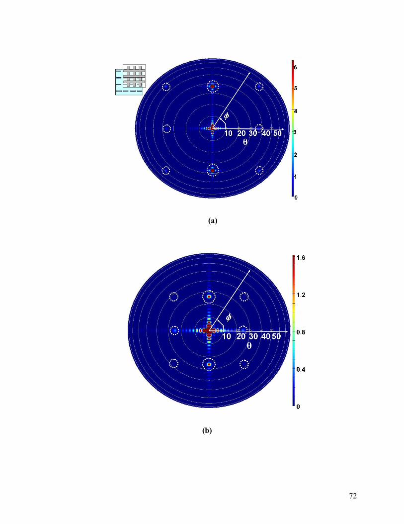
72
(a)
(b)
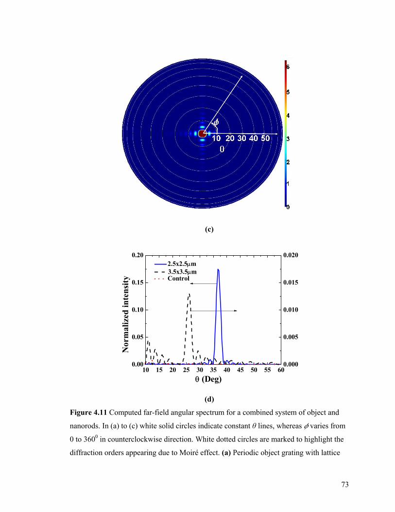
73
(c)
10 15 20 25 30 35 40 45 50 55 600.00
0.05
0.10
0.15
0.20
Nor
mal
ized
inte
nsity
θ (Deg)
2.5x2.5μm
Control
0.000
0.005
0.010
0.015
0.020
3.5x3.5μm
(d)
Figure 4.11 Computed far-field angular spectrum for a combined system of object and
nanorods. In (a) to (c) white solid circles indicate constant θ lines, whereas f varies from
0 to 3600 in counterclockwise direction. White dotted circles are marked to highlight the
diffraction orders appearing due to Moiré effect. (a) Periodic object grating with lattice
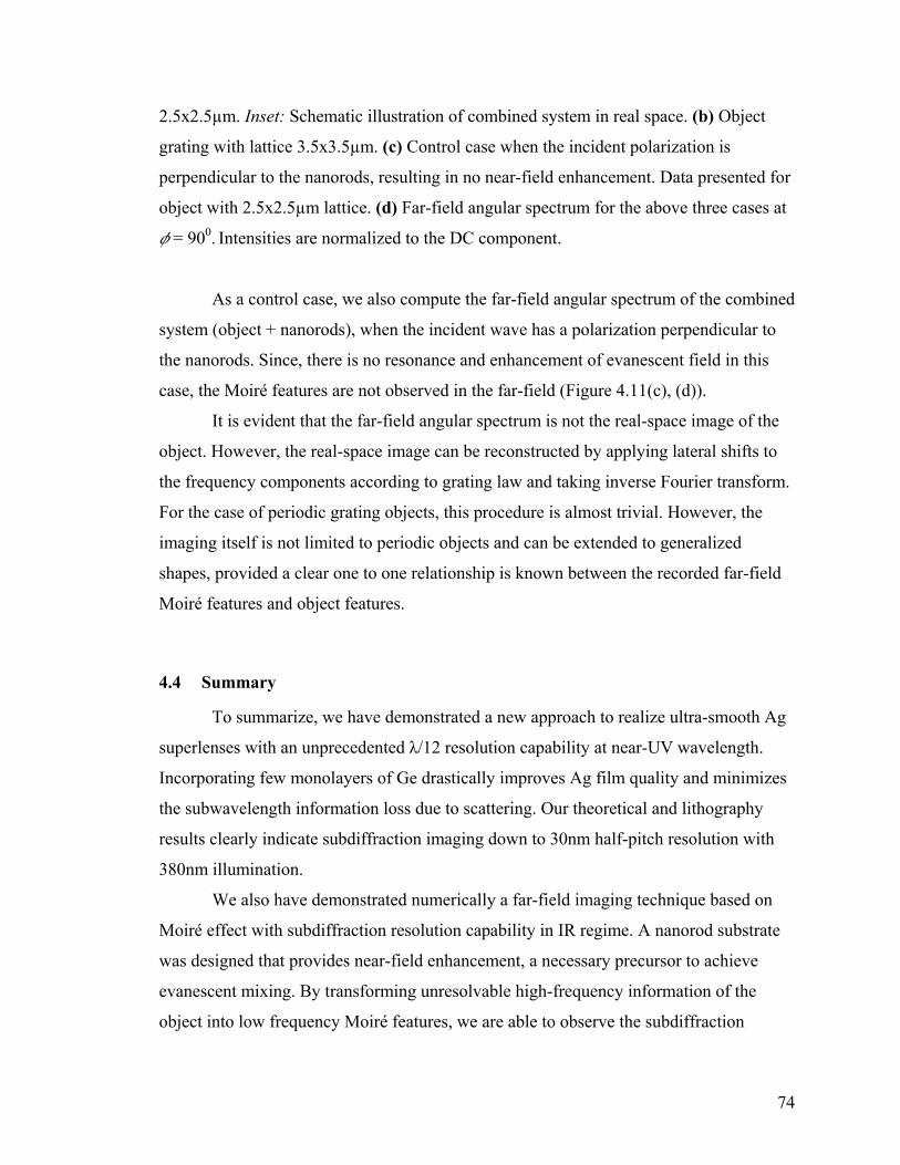
74
2.5x2.5µm. Inset: Schematic illustration of combined system in real space. (b) Object
grating with lattice 3.5x3.5µm. (c) Control case when the incident polarization is
perpendicular to the nanorods, resulting in no near-field enhancement. Data presented for
object with 2.5x2.5µm lattice. (d) Far-field angular spectrum for the above three cases at
f = 900. Intensities are normalized to the DC component.
As a control case, we also compute the far-field angular spectrum of the combined
system (object + nanorods), when the incident wave has a polarization perpendicular to
the nanorods. Since, there is no resonance and enhancement of evanescent field in this
case, the Moiré features are not observed in the far-field (Figure 4.11(c), (d)).
It is evident that the far-field angular spectrum is not the real-space image of the
object. However, the real-space image can be reconstructed by applying lateral shifts to
the frequency components according to grating law and taking inverse Fourier transform.
For the case of periodic grating objects, this procedure is almost trivial. However, the
imaging itself is not limited to periodic objects and can be extended to generalized
shapes, provided a clear one to one relationship is known between the recorded far-field
Moiré features and object features.
4.4 Summary
To summarize, we have demonstrated a new approach to realize ultra-smooth Ag
superlenses with an unprecedented λ/12 resolution capability at near-UV wavelength.
Incorporating few monolayers of Ge drastically improves Ag film quality and minimizes
the subwavelength information loss due to scattering. Our theoretical and lithography
results clearly indicate subdiffraction imaging down to 30nm half-pitch resolution with
380nm illumination.
We also have demonstrated numerically a far-field imaging technique based on
Moiré effect with subdiffraction resolution capability in IR regime. A nanorod substrate
was designed that provides near-field enhancement, a necessary precursor to achieve
evanescent mixing. By transforming unresolvable high-frequency information of the
object into low frequency Moiré features, we are able to observe the subdiffraction
75
features in the far-field. At incident wavelength of 6µm, Moiré features corresponding to
object periodicity of 2.5µm were clearly seen in the far-field. The methodology relies on
a prerequisite that an unambiguous reconstruction can be done by a suitable design of
metamaterial substrate. The image reconstruction procedure is very simple and requires
only Fourier transform and lateral shifts of frequency components. This reconstruction
procedure can be completely automated, making real time dynamic imaging of materials,
biological cells and tissues with subwavelength resolution a distinct possibility.
Methods
Sample preparation for smooth superlens:
Ag, Ag/Ge samples were prepared on quartz using electron-beam evaporation
with deposition rate of 0.1 Å/s for Ge and 1 Å/s for Ag at a pressure of 8x10⁻⁷ torr. The
substrate (~1"x1", 1mm thick) were first cleaned using RCA1 solution.91 Electronic grade
source material was supplied by Kurt J. Lesker with a four-nine purity.
Nanoimprint technology:
Nanoimprint technology developed at Hewlett-Packard laboratory was utilized to
fabricate 30nm half-pitch Cr gratings and 6nm thick spacer films. First a PMMA
(950k/15k) layer with thickness 60nm is spin coated on quartz substrate, followed by spin
coating of a UV-resist with thickness 66nm. The UV-resist is imprinted and cured using a
mold with 30nm half-pitch gratings. UV-resist layer is then etched to 45nm thickness
using RIE (with CF4: 60 sccm, 2mtorr), followed by through etching of PMMA layer
with O2 RIE (40 sccm, 2mtorr). 40nm thick Cr is deposited using e-beam evaporator at
0.1Å/s, followed by liftoff using acetone and ultrasonic agitation. Planarization of the Cr
gratings is performed by spin coating UV-resist with thickness 66nm, followed by
imprinting with a flat mold and UV-curing. UV-resist is then etched using CF4 RIE to a
total thickness of 46nm, thus resulting in a spacer layer with 6nm thickness.

76
XRR measurement:
X-ray reflectivity measurements were carried out on a Philip MRD X'pert system.
Measurements were made in a range between 0 and 3 degrees, of which some data points
close to zero degree were removed since no useful information is available until the total
angle of reflection. Incident angle scan data points were collected with a step width of
0.01 degrees. Theoretical curves were simulated using commercial software Wingixa.
Film thickness and density were determined from the period of intensity oscillations and
total reflection edge, respectively.
77
5 SUMMARY, FUTURE WORK AND OUTLOOK
5.1 Summary
This dissertation has dealt with design and characterization of plasmonic
metamaterials. We have addressed some of the fascinating applications of metamaterials
in realizing new optical devices which are considerably smaller than light wavelength.
We have investigated a novel characterization technique specifically suited to probe
optical properties of metamaterials at the nanoscale.
After a brief overview of recent advances in the field of optical metamaterials in
introduction chapter, we presented an integrated metamaterial modulator for on-fiber data
transport and telecommunication applications in Chapter 2. With numerical simulations
we demonstrated a double-wire sandwich structure, popularly known as a “fishnet
metamaterial”, as an effective modulator. We have also investigated a flipped fishnet
design that shows promise of being a low-loss and more effective integrated modulator.
Chapter 3 describes scanning electron beam based cathodoluminescence imaging
and spectroscopy technique for characterization of plasmonic metamaterials. Both
experimental and numerical simulation studies were presented that reveals a coherent
picture of excitation of plasmon modes with electron beam. We have conceptualized a
new finite-difference time-domain based simulation methodology that models the
electron beam as an array of point dipoles. In this chapter we focused on analyzing
plasmon modes of silver triangular nanoparticles anchored on a substrate.
In Chapter 4 we discussed the subdiffraction imaging capability of plasmonic
systems such as planar silver superlenses and nanorods. We have experimentally
demonstrated a resolution capability of 1/12th of the illumination wavelength, providing
unprecedented image details up to 30nm with near-UV light. This was achieved by
carefully minimizing the information losses due to evanescent decay, absorption and
scattering due to rough surfaces. Applying the state-of-the-art nanoimprint technology
and intermediate wetting layer (germanium) for the growth of silver, we have shown that
a smooth superlens could be fabricated with thickness down to 15nm. We have also
discussed extending the subdiffraction resolution capability of plasmonic materials to far-
78
field in infrared regime for chemical sensing applications. By designing a nanorod
substrate, we have numerically demonstrated that the evanescent modes from an object
can be coupled out to the far-field in the form of Moiré features. A subdiffraction
resolution of 2.5µm pitch is demonstrated at 6µm wavelength.
5.2 Future work
This work presents a unique platform to understand the fundamental
characteristics of metamaterials and harness the novel physics to develop practical
applications. The field of optical metamaterials is relatively new, and there is certainly a
huge scope for further development on several aspects presented in this study.
Specifically there are certain key directions which we would like to be followed-up:
- Experimental demonstration of integrated fiber modulator, including
study of temporal dynamics.
- Exploration of novel plasmon physics of metallic nanostructures with
cathodoluminescence spectroscopy, including study of plasmon
propagation lengths to distinguish localized vs. traveling plasmon
modes. Improving the modeling and numerical simulation methodology
by incorporating varying electron velocity, and dispersive or lossy
substrates.
- Experimental realization of far-field subdiffraction imaging at infrared
wavelengths and developments of efficient image reconstruction
algorithms for complex subwavelength structures.
5.3 Outlook
Since the realization of metamaterials first at microwave frequencies, significant
improvements in performance have been made possible by new physical insights in
device design and better fabrication techniques. However, material losses at optical
frequencies remain a key challenge to the wide-scale adoption of metamaterial enabled
technologies. For example, current commercial telecommunication switches operate with
more than 10dB extinction ratios. While metamaterials offer an opportunity to
79
significantly reduce the device footprints, further exploration of design optimization to
reduce losses and harness other novel nonlinear behavior is desirable. The development
of low-loss metamaterials could be the foundation of switches, modulators and other
novel optical devices in all-optical integrated information processing architectures, which
can process data signals much more efficiently than their electronic counterparts.
In addition, the fundamental understanding of light-matter interaction at small
scales is still an area open to debate. The boundary between continuum and quantum
mechanical phenomena can be challenged with development of characterization
techniques such as cathodoluminescence and electron energy loss spectroscopy. This is
critical for development of miniaturized optical devices such as chemical sensors with
single molecule detection sensitivity and waveguides to confine and guide
electromagnetic signals at nanoscale.
Fabrication of sub-20nm thick smooth silver films is critical for many
applications in metamaterials, plasmonics and nanophotonics. This includes realization of
multilayer superlenses operating at visible wavelengths. Development of potential low-
loss and high resolution superlenses opens the door to exciting applications in nanoscale
optical metrology and nanomanufacturing. The ultrahigh resolution capability of far-field
superlenses could have a far reaching impact on biomedical imaging and chemical
sensing.
Demonstration of novel functionalities and applications at research scale is only
the beginning of the road for metamaterials. The control of optical properties at nanoscale
and integration of different components remain one of the hardest challenges.
Nevertheless, the progress made in metamaterials over a relatively short period of time is
phenomenal. The realization of full potential of this new class of materials will have a
profound impact on several disciplines including electronics, communication, medical
diagnostics, health care, and manufacturing.
80
REFERENCES
1. The top ten advances in materials science. Mater. Today 2008, 11, 40-45.
2. Chaturvedi, P.; Hsu, K.; Zhang, S.; Fang, N., New Frontiers of Metamaterials:
Design and Fabrication. MRS Bull. 2008, 33, 915-920.
3. Veselago, V. G., The electrodynamics of substances with simultaneously negative
values of ε and μ. Sov. Phys. Usp. 1968, 10, 509.
4. Shelby, R. A.; Smith, D. R.; Schultz, S., Experimental Verification of a Negative
Index of Refraction. Science 2001, 292, 77-79.
5. Yen, T. J.; Padilla, W. J.; Fang, N.; Vier, D. C.; Smith, D. R.; Pendry, J. B.;
Basov, D. N.; Zhang, X., Terahertz magnetic response from artificial materials. Science
2004, 303, 1494-1496.
6. Smith, D. R.; Pendry, J. B.; Wiltshire, M. C. K., Metamaterials and negative
refractive index. Science 2004, 305, 788-792.
7. Smith, D. R.; Padilla, W. J.; Vier, D. C.; Nemat-Nasser, S. C.; Schultz, S.,
Composite medium with simultaneously negative permeability and permittivity. Phys.
Rev. Lett. 2000, 84, 4184-4187.
8. Greegor, R. B.; Parazzoli, C. G.; Li, K.; Tanielian, M. H., Origin of dissipative
losses in negative index of refraction materials. Appl. Phys. Lett. 2003, 82, 2356-2358.
9. Fang, N.; Lee, H.; Sun, C.; Zhang, X., Sub-diffraction-limited optical imaging
with a silver superlens. Science 2005, 308, 534-537.
10. Chen, H. S.; Wu, B. I.; Zhang, B.; Kong, J. A., Electromagnetic wave interactions
with a metamaterial cloak. Phys. Rev. Lett. 2007, 99, 063903.
11. Williams, C. R.; Andrews, S. R.; Maier, S. A.; Fernandez-Dominguez, A. I.;
Martin Moreno, L.; Garcia-Vidal, F. J., Highly confined guiding of terahertz surface
plasmon polaritons on structured metal surfaces. Nature Photonics 2008, 2, 175-179.
12. Alu, A.; Salandrino, A.; Engheta, N., Negative effective permeability and left-
handed materials at optical frequencies. Optics Express 2006, 14, 1557-1567.
13. Logeeswaran, V. J.; Stameroff, A. N.; Islam, M. S.; Wu, W.; Bratkovsky, A. M.;
Kuekes, P. J.; Wang, S. Y.; Williams, R. S., Switching between positive and negative
81
permeability by photoconductive coupling for modulation of electromagnetic radiation.
Appl. Phys. A: Mater. Sci. Process. 2007, 87, 209-216.
14. Wu, W.; Yu, Z. N.; Wang, S. Y.; Williams, R. S.; Liu, Y. M.; Sun, C.; Zhang, X.;
Kim, E.; Shen, Y. R.; Fang, N. X., Midinfrared metamaterials fabricated by nanoimprint
lithography. Appl. Phys. Lett. 2007, 90, 063107.
15. Zhou, J.; Koschny, T.; Kafesaki, M.; Economou, E. N.; Pendry, J. B.; Soukoulis,
C. M., Saturation of the magnetic response of split-ring resonators at optical frequencies.
Phys. Rev. Lett. 2005, 95, 223902.
16. Dolling, G.; Enkrich, C.; Wegener, M.; Soukoulis, C. M.; Linden, S.,
Simultaneous negative phase and group velocity of light in a metamaterial. Science 2006,
312, 892-894.
17. Lezec, H. J.; Dionne, J. A.; Atwater, H. A., Negative Refraction at Visible
Frequencies. Science 2007, 316, 430-432.
18. Shin, H.; Fan, S. H., All-angle negative refraction for surface plasmon waves
using a metal-dielectric-metal structure. Phys. Rev. Lett. 2006, 96, 073907.
19. Fang, N.; Liu, Z. W.; Yen, T. J.; Zhang, X., Regenerating evanescent waves from
a silver superlens. Optics Express 2003, 11, 682-687.
20. Shalaev, V. M., Optical negative-index metamaterials. Nature Photonics 2007, 1,
41-48.
21. Ebbesen, T. W.; Lezec, H. J.; Ghaemi, H. F.; Thio, T.; Wolff, P. A., Extraordinary
optical transmission through sub-wavelength hole arrays. Nature 1998, 391, 667-669.
22. Nie, S. M.; Emery, S. R., Probing single molecules and single nanoparticles by
surface-enhanced Raman scattering. Science 1997, 275, 1102-1106.
23. Pendry, J. B.; Martin-Moreno, L.; Garcia-Vidal, F. J., Mimicking surface
plasmons with structured surfaces. Science 2004, 305, 847-848.
24. Pendry, J. B., Negative refraction makes a perfect lens. Phys. Rev. Lett. 2000, 85,
3966-3969.
25. Ramakrishna, S. A.; Pendry, J. B.; Wiltshire, M. C. K.; Stewart, W. J., Imaging
the near field. J. Mod. Opt. 2003, 50, 1419-1430.
26. Chaturvedi, P.; Fang, N., Molecular scale imaging with a multilayer superlens. In
Mater. Res. Soc. Symp. Proc., 2006; Vol. 919, pp 0919-J04-07.
82
27. Basile, L.; Hawoong, H.; Czoschke, P.; Chiang, T. C., X-ray studies of the growth
of smooth Ag films on Ge(111)-c(2 x 8). Appl. Phys. Lett. 2004, 84, 4995-4997.
28. Pendry, J. B.; Holden, A. J.; Stewart, W. J.; Youngs, I., Extremely low frequency
plasmons in metallic mesostructures. Phys. Rev. Lett. 1996, 76, 4773-4776.
29. Chen, H. T.; Padilla, W. J.; Zide, J. M. O.; Gossard, A. C.; Taylor, A. J.; Averitt,
R. D., Active terahertz metamaterial devices. Nature 2006, 444, 597-600.
30. Chettiar, U. K.; Xiao, S.; Kildishev, A. V.; Cai, W.; Yuan, H. K.; Drachev, V. P.;
Shalaev, V. M., Optical Metamagnetism and Negative-index Metamaterials. MRS Bull.
2008, 33, 921-926.
31. Valentine, J.; Zhang, S.; Zentgraf, T.; Ulin-Avila, E.; Genov, D. A.; Bartal, G.;
Zhang, X., Three-dimensional optical metamaterial with a negative refractive index.
Nature 2008, 455, 376-379.
32. Kim, E.; Shen, Y. R.; Wu, W.; Ponizovskaya, E.; Yu, Z.; Bratkovsky, A. M.;
Wang, S. Y.; Williams, R. S., Modulation of negative index metamaterials in the near-IR
range. Appl. Phys. Lett. 2007, 91, 173105.
33. Weiland, T.; Schuhmann, R.; Greegor, R. B.; Parazzoli, C. G.; Vetter, A. M.;
Smith, D. R.; Vier, D. C.; Schultz, S., Ab initio numerical simulation of left-handed
metamaterials: Comparison of calculations and experiments. J. Appl. Phys. 2001, 90,
5419-5424.
34. Smith, D. R.; Schultz, S.; Markos, P.; Soukoulis, C. M., Determination of
effective permittivity and permeability of metamaterials from reflection and transmission
coefficients. Phys. Rev. B 2002, 65, 5.
35. Wu, W.; Kim, E.; Ponizovskaya, E.; Liu, Y.; Yu, Z.; Fang, N.; Shen, Y. R.;
Bratkovsky, A. M.; Tong, W.; Sun, C., et al., Optical metamaterials at near and mid-IR
range fabricated by nanoimprint lithography. Appl. Phys. A: Mater. Sci. Process. 2007,
87, 143-150.
36. Klar, T. A.; Kildishev, A. V.; Drachev, V. P.; Shalaev, V. M., Negative-index
metamaterials: going optical. IEEE J. Sel. Top. Quantum Electron. 2006, 12, 1106-1115.
37. Ponizovskaya, E. V.; Bratkovsky, A. M., Negative index materials with gain
media for fast modulation. Appl. Phys. A: Mater. Sci. Process. 2009, 95, 1137-1142.
83
38. Zhang, S.; Fan, W.; Panoiu, N. C.; Malloy, K. J.; Osgood, R. M.; Brueck, S. R.,
Optical negative-index bulk metamaterials consisting of 2D perforated metal-dielectric
stacks. Optics Express 2006, 14, 6778-6787.
39. Schurig, D., Off-normal incidence simulations of metamaterials using FDTD.
International Journal of Numerical Modelling: Electronic Networks, Devices and Fields
2006, 19.
40. http://www.lumerical.com
41. Haes, A. J.; Van Duyne, R. P., A nanoscale optical blosensor: Sensitivity and
selectivity of an approach based on the localized surface plasmon resonance spectroscopy
of triangular silver nanoparticles. J. Am. Chem. Soc. 2002, 124, 10596-10604.
42. McFarland, A. D.; Van Duyne, R. P., Single silver nanoparticles as real-time
optical sensors with zeptomole sensitivity. Nano Lett. 2003, 3, 1057-1062.
43. Bharadwaj, P.; Novotny, L., Spectral dependence of single molecule fluorescence
enhancement. Optics Express 2007, 15, 14266-14274.
44. Ishi, T.; Fujikata, J.; Makita, K.; Baba, T.; Ohashi, K., Si nano-photodiode with a
surface plasmon antenna. Japanese Journal of Applied Physics Part 2-Letters & Express
Letters 2005, 44, L364-L366.
45. Eftekhari, F.; Gordon, R., Enhanced second harmonic generation from
noncentrosymmetric nanohole arrays in a gold film. IEEE J. Sel. Top. Quantum Electron.
2008, 14, 1552-1558.
46. Kim, S.; Jin, J. H.; Kim, Y. J.; Park, I. Y.; Kim, Y.; Kim, S. W., High-harmonic
generation by resonant plasmon field enhancement. Nature 2008, 453, 757-760.
47. Haes, A. J.; Haynes, C. L.; McFarland, A. D.; Schatz, G. C.; Van Duyne, R. R.;
Zou, S. L., Plasmonic materials for surface-enhanced sensing and spectroscopy. MRS
Bull. 2005, 30, 368-375.
48. Yin, L.; Vlasko-Vlasov, V. K.; Rydh, A.; Pearson, J.; Welp, U.; Chang, S. H.;
Gray, S. K.; Schatz, G. C.; Brown, D. B.; Kimball, C. W., Surface plasmons at single
nanoholes in Au films. Appl. Phys. Lett. 2004, 85, 467-469.
49. Nelayah, J.; Kociak, M.; Stephan, O.; de Abajo, F. J. G.; Tence, M.; Henrard, L.;
Taverna, D.; Pastoriza-Santos, I.; Liz-Marzan, L. M.; Colliex, C., Mapping surface
plasmons on a single metallic nanoparticle. Nature Physics 2007, 3, 348-353.
84
50. Gomez-Medina, R.; Yamamoto, N.; Nakano, M.; Abajo, F. J. G., Mapping
plasmons in nanoantennas via cathodoluminescence. New J. Phys. 2008, 10, 105009.
51. Hofmann, C. E.; Vesseur, E. J. R.; Sweatlock, L. A.; Lezec, H. J.; Garcia de
Abajo, F. J.; Polman, A.; Atwater, H. A., Plasmonic modes of annular nanoresonators
imaged by spectrally resolved cathodoluminescence. Nano Lett. 2007, 7, 3612-3617.
52. Yamamoto, N.; Araya, K.; de Abajo, F. J. G., Photon emission from silver
particles induced by a high-energy electron beam. Phys. Rev. B 2001, 64, 205419.
53. Yamamoto, N.; Nakano, M.; Suzuki, T., Light emission by surface plasmons on
nanostructures of metal surfaces induced by high-energy electron beams. Surf. Interface
Anal. 2006, 38, 1725-1730.
54. Cibert, J.; Petroff, P. M.; Dolan, G. J.; Pearton, S. J.; Gossard, A. C.; English, J.
H., Optically detected carrier confinement to one and zero dimension in GaAs quantum
well wires and boxes. Appl. Phys. Lett. 1986, 49, 1275-1277.
55. Chichibu, S.; Wada, K.; Nakamura, S., Spatially resolved cathodoluminescence
spectra of InGaN quantum wells. Appl. Phys. Lett. 1997, 71, 2346-2348.
56. Leon, R.; Petroff, P. M.; Leonard, D.; Fafard, S., Spatially Resolved Visible
Luminescence of Self-Assembled Semiconductor Quantum Dots. Science 1995, 267,
1966-1968.
57. Rodriguez-Viejo, J.; Jensen, K. F.; Mattoussi, H.; Michel, J.; Dabbousi, B. O.;
Bawendi, M. G., Cathodoluminescence and photoluminescence of highly luminescent
CdSe/ZnS quantum dot composites. Appl. Phys. Lett. 1997, 70, 2132-2134.
58. García de Abajo, F. J.; Howie, A., Relativistic Electron Energy Loss and
Electron-Induced Photon Emission in Inhomogeneous Dielectrics. Phys. Rev. Lett. 1998,
80, 5180.
59. Haynes, C. L.; Van Duyne, R. P., Plasmon-sampled surface-enhanced Raman
excitation spectroscopy. J. Phys. Chem. B 2003, 107, 7426-7433.
60. McFarland, A. D.; Young, M. A.; Dieringer, J. A.; Van Duyne, R. P.,
Wavelength-scanned surface-enhanced Raman excitation spectroscopy. J. Phys. Chem. B
2005, 109, 11279-11285.
61. Shuford, K. L.; Ratner, M. A.; Schatz, G. C., Multipolar excitation in triangular
nanoprisms. J. Chem. Phys. 2005, 123, 114713.
85
62. Hao, E.; Schatz, G. C., Electromagnetic fields around silver nanoparticles and
dimers. J. Chem. Phys. 2004, 120, 357-366.
63. Martin, O. J. F., Plasmon Resonances in Nanowires with a Non-regular Cross-
Section. In Optical Nanotechnologies, Tominaga, J.; Tsai, D. P., Eds. Springer-Verlag:
Berlin Heidelberg, 2003; pp 183-210.
64. Nelayah, J.; Gu, L.; Sigle, W.; Koch, C. T.; Pastoriza-Santos, I.; Liz-Marzán, L.
M.; van Aken, P. A., Direct imaging of surface plasmon resonances on single triangular
silver nanoprisms at optical wavelength using low-loss EFTEM imaging. Opt. Lett. 2009,
34, 1003-1005.
65. Rang, M.; Jones, A. C.; Zhou, F.; Li, Z. Y.; Wiley, B. J.; Xia, Y. N.; Raschke, M.
B., Optical Near-Field Mapping of Plasmonic Nanoprisms. Nano Lett. 2008, 8, 3357-
3363.
66. Raether, H., Surface-Plasmons on Smooth and Rough Surfaces and on Gratings.
1988; Vol. 111, p 1-133.
67. Garcia de Abajo, F. J.; Kociak, M., Probing the photonic local density of states
with electron energy loss spectroscopy. Phys. Rev. Lett. 2008, 100, 106804.
68. Johnson, P. B.; Christy, R. W., Optical constants of noble metals. Phys. Rev. B
1972, 6, 4370-4379.
69. Sherry, L. J.; Jin, R. C.; Mirkin, C. A.; Schatz, G. C.; Van Duyne, R. P., Localized
surface plasmon resonance spectroscopy of single silver triangular nanoprisms. Nano
Lett. 2006, 6, 2060-2065.
70. Hsu, K. H.; Schultz, P. L.; Ferreira, P. M.; Fang, N. X., Electrochemical
Nanoimprinting with Solid-State Superionic Stamps. Nano Lett. 2007, 7, 446-451.
71. Palik, E. D., Handbook of optical constants. 1984; Vol. 1.
72. Fang, N. Engineering Subwavelength Photonic Meta Structures and Devices. PhD
thesis, 2004.
73. Lee, H.; Xiong, Y.; Fang, N.; Srituravanich, W.; Durant, S.; Ambati, M.; Sun, C.;
Zhang, X., Realization of optical superlens imaging below the diffraction limit. New J.
Phys. 2005, 7, 255.
74. Logeeswaran, V. J.; Chan, M. L.; Bayam, Y.; Saif Islam, M.; Horsley, D. A.; Li,
X.; Wu, W.; Wang, S. Y.; Williams, R. S., Ultra-smooth metal surfaces generated by
86
pressure-induced surface deformation of thin metal films. Appl. Phys. A: Mater. Sci.
Process. 2007, 87, 187-192.
75. Logeeswaran, V. J.; Kobayashi, N. P.; Islam, M. S.; Wu, W.; Chaturvedi, P.;
Fang, N. X.; Wang, S. Y.; Williams, R. S., Ultrasmooth Silver Thin Films Deposited with
a Germanium Nucleation Layer. Nano Lett. 2009, 9, 178-182.
76. Heavens, O. S., Optical Properties of Thin Solid Films. Dover: New York, 1991.
77. Madou, M. J., Fundamentals of Microfabrication, Chapter 1. 2nd ed.; CRC Press:
2002.
78. Taubner, T.; Korobkin, D.; Urzhumov, Y.; Shvets, G.; Hillenbrand, R., Near-
Field Microscopy Through a SiC Superlens. Science 2006, 313, 1595.
79. Liu, Z.; Durant, S.; Lee, H.; Pikus, Y.; Fang, N.; Xiong, Y.; Sun, C.; Zhang, X.,
Far-Field Optical Superlens. Nano Lett. 2007, 7, 403-408.
80. Jacob, Z.; Alekseyev, L. V.; Narimanov, E., Optical Hyperlens: Far-field imaging
beyond the diffraction limit. Optics Express 2006, 14, 8247-8256.
81. Alessandro, S.; Nader, E., Far-field subdiffraction optical microscopy using
metamaterial crystals: Theory and simulations. Phys. Rev. B 2006, 74, 075103.
82. Liu, Z. W.; Lee, H.; Xiong, Y.; Sun, C.; Zhang, X., Far-field optical hyperlens
magnifying sub-diffraction-limited objects. Science 2007, 315, 1686-1686.
83. Smolyaninov, I. I.; Hung, Y.-J.; Davis, C. C., Magnifying Superlens in the Visible
Frequency Range. Science 2007, 315, 1699-1701.
84. Liu, Z. W.; Durant, S.; Lee, H.; Xiong, Y.; Pikus, Y.; Sun, C.; Zhang, X., Near-
field Moire effect mediated by surface plasmon polariton excitation. Opt. Lett. 2007, 32,
629-631.
85. Flanders, D. C.; Smith, H. I.; Austin, S., New Interferometric Alignment
Technique. Appl. Phys. Lett. 1977, 31, 426-428.
86. Grimm, M. A.; Lohmann, A. W., Superresolution Image for One-Dimensional
Objects. J. Opt. Soc. Am. 1966, 56, 1151-1156.
87. Durant, S.; Liu, Z. W.; Steele, J. A.; Zhang, X., Theory of the transmission
properties of an optical far-field superlens for imaging beyond the diffraction limit. J.
Opt. Soc. Am. B 2006, 23, 2383-2392.

87
88. Neubrech, F.; Kolb, T.; Lovrincic, R.; Fahsold, G.; Pucci, A.; Aizpurua, J.;
Cornelius, T. W.; Toimil-Molares, M. E.; Neumann, R.; Karim, S., Resonances of
individual metal nanowires in the infrared. Appl. Phys. Lett. 2006, 89, 253104-3.
89. Neubrech, F.; Pucci, A.; Cornelius, T. W.; Karim, S.; Garcia-Etxarri, A.;
Aizpurua, J., Resonant Plasmonic and Vibrational Coupling in a Tailored Nanoantenna
for Infrared Detection. Phys. Rev. Lett. 2008, 101, 157403-4.
90. Mandel, L.; Wolf, E., Optical coherence and Quantum Optics. Cambridge
University Press: 1995.
91. Kern, W., Handbook of Semiconductor Cleaning Technology. Noyes Publishing:
Park Ridge, NJ, 1993.
88
AUTHOR’S BIOGRAPHY
Pratik Chaturvedi was born on June 26th, 1983 in Madhya Pradesh, India. He
received his B.Tech. degree in Mechanical Engineering from the Indian Institute of
Technology (IIT) Bombay, Mumbai, India in 2004. Pratik then joined Department of
Mechanical Engineering at University of Illinois, Urbana-Champaign in fall 2004. He
worked with Prof. Nicholas Fang in the area of Nanoplasmonics and graduated with his
M.S. in 2006. Pratik then continued with graduate studies towards Ph.D. degree under the
guidance of Prof. Fang. His research has focused on design and characterization of
optical metamaterials and has resulted in several conference presentations and journal
publications including in MRS Bulletin and Nano Letters. Two of his papers are currently
under consideration for publication in Nano Letters and ACS Nano. After receiving his
Ph.D., Pratik will join Intel Corporation in Portland, Oregon as senior R&D process
engineer.
Related Documents