RAPID COMMUNICATIONS PHYSICAL REVIEW B 94, 081406(R) (2016) Designing electron spin textures and spin interferometers by shape deformations Zu-Jian Ying, 1, 2 Paola Gentile, 1 Carmine Ortix, 3, 4 and Mario Cuoco 1 1 CNR-SPIN and Dipartimento di Fisica “E. R. Caianiello,” Universit` a di Salerno, I-84084 Fisciano (Salerno), Italy 2 Beijing Computational Science Research Center, Beijing 100084, China 3 Institute for Theoretical Solid State Physics, IFW-Dresden, Helmholtzstraße 20, D-01069 Dresden, Germany 4 Institute for Theoretical Physics, Center for Extreme Matter and Emergent Phenomena, Utrecht University, Princetonplein 5, 3584 CC Utrecht, The Netherlands (Received 7 March 2016; revised manuscript received 26 May 2016; published 11 August 2016) We demonstrate that the spin orientation of an electron propagating in a one-dimensional nanostructure with Rashba spin-orbit (SO) coupling can be manipulated on demand by changing the geometry of the nanosystem. Shape deformations that result in a nonuniform curvature give rise to complex three-dimensional spin textures in space. We employ the paradigmatic example of an elliptically deformed quantum ring to unveil the way to get an all-geometrical and all-electrical control of the spin orientation. The resulting spin textures exhibit a tunable topological character with windings around the radial and the out-of-plane directions. We show that these topologically nontrivial spin patterns affect the spin interference effect in the deformed ring, thereby resulting in different geometry-driven ballistic electronic transport behaviors. Our results establish a deep connection between electronic spin textures, spin transport, and the nanoscale shape of the system. DOI: 10.1103/PhysRevB.94.081406 Introduction. The manipulation and control of the electron spin are essential ingredients for the development of innovative quantum-engineered devices [1–3]. The spin-orbit (SO) cou- pling [4–6] is particularly attractive in this framework because it offers the promising prospect [7] of an all-electrical intrinsic control over the spin without applying a magnetic field. For low-dimensional nanosystems with structure inversion asymmetry, this coupling between the orbital motion and the electron spin is due to the so-called Rashba SO interaction [4–6]. The Rashba SO coupling is at the heart of a growing research interest for the spin generation, manipulation, and detection due to the tantalizing possibilities of tuning the spin orientation through the electron propagation and vice versa to exert a spin control of the electron trajectories. Central consequences of these constituent features are, among the many possibilities, the spin Hall [8,9] and the spin galvanic effects [10–12], the SO driven spin torque [13,14], the design of quantum topological states [15], etc. Charge carriers in materials with Rashba SO are subject to a momentum dependent effective magnetic field which not only results in spin-dependent velocity but also in a nontrivial geometric phase. Such phase is another important means to manipulate the electron spin. For instance, in the Aharonov-Casher (AC) effect [16], magnetic dipoles moving around a tube of electric charge acquire a nontrivial Berry [17] or geometric phase [18], being similar to the case of the Aharonov-Bohm [19] effect for charged particles moving in a closed circuit around a magnetic flux. With the development of semiconducting nanostructures, a possibility has emerged to tune quantum states by combining Rashba effects and geometric phases. Considering the role of magnetic field Published by the American Physical Society under the terms of the Creative Commons Attribution 3.0 License. Further distribution of this work must maintain attribution to the author(s) and the published article’s title, journal citation, and DOI. textures in driving a spin geometric phase [20], the effects of quantum geometric phases have been predicted [21] and experimentally observed in the transport properties of semi- conducting quantum rings [22,23]. Such findings opened the path to a spin topological design [24], as demonstrated by the magnetic field driven topological transition in the geometric phase and the consequences on the spin transport [23,25]. In view of the rapid progress in nanostructuring techniques, it would be highly challenging and desirable to design nanos- tructures where the system geometry is the main knob to tailor the electron spin properties. In this Rapid Communication, we demonstrate that the curvature of a nanostructure with Rashba SO coupling allows one to manipulate and control the spin orientation and the spin transport. We use the prototypical geometry of elliptical quantum rings to unveil complex three-dimensional spin textures in space and how they evolve in the presence of a nonuniform curvature. The resulting spin patterns have distinct topological features with tunable windings around the radial and the out-of-plane spin directions along the elliptical ring. Remarkably, we find different types of transitions between quantum states with inequivalent spin textures by varying the curvature strength or the Rashba SO coupling thus indicating a unique path to control the electron spin in curved nanostructures. We then demonstrate a fundamental twist between curvature, spin texture, and spin transport Curvature-driven spin torques. Electrons confined to move along a one-dimensional planarly curved nanostructure [Fig. 1(a)] are subject to a Rashba SO interaction, due to the inversion symmetry breaking that, as for the case of a straight nanostructure, couples the orbital momentum and the local spin component that is normal to the electron motion [26]. Since the nanostructure has a nontrivial curvature, the local normal spin direction depends on the position and thus generally it does not commute with the momentum. Such interplay can be conveniently expressed by introducing the local normal ˆ N (s ) and tangential ˆ T (s ) directions at a given position s along the curve, as well as the related local Pauli matrices σ N (s ) = τ · ˆ N (s ) and σ T (s ) = τ · ˆ T (s ) 2469-9950/2016/94(8)/081406(5) 081406-1 Published by the American Physical Society

Welcome message from author
This document is posted to help you gain knowledge. Please leave a comment to let me know what you think about it! Share it to your friends and learn new things together.
Transcript
RAPID COMMUNICATIONS
PHYSICAL REVIEW B 94, 081406(R) (2016)
Designing electron spin textures and spin interferometers by shape deformations
Zu-Jian Ying,1,2 Paola Gentile,1 Carmine Ortix,3,4 and Mario Cuoco1
1CNR-SPIN and Dipartimento di Fisica “E. R. Caianiello,” Universita di Salerno, I-84084 Fisciano (Salerno), Italy2Beijing Computational Science Research Center, Beijing 100084, China
3Institute for Theoretical Solid State Physics, IFW-Dresden, Helmholtzstraße 20, D-01069 Dresden, Germany4Institute for Theoretical Physics, Center for Extreme Matter and Emergent Phenomena, Utrecht University,
Princetonplein 5, 3584 CC Utrecht, The Netherlands(Received 7 March 2016; revised manuscript received 26 May 2016; published 11 August 2016)
We demonstrate that the spin orientation of an electron propagating in a one-dimensional nanostructure withRashba spin-orbit (SO) coupling can be manipulated on demand by changing the geometry of the nanosystem.Shape deformations that result in a nonuniform curvature give rise to complex three-dimensional spin texturesin space. We employ the paradigmatic example of an elliptically deformed quantum ring to unveil the way toget an all-geometrical and all-electrical control of the spin orientation. The resulting spin textures exhibit atunable topological character with windings around the radial and the out-of-plane directions. We show that thesetopologically nontrivial spin patterns affect the spin interference effect in the deformed ring, thereby resultingin different geometry-driven ballistic electronic transport behaviors. Our results establish a deep connectionbetween electronic spin textures, spin transport, and the nanoscale shape of the system.
DOI: 10.1103/PhysRevB.94.081406
Introduction. The manipulation and control of the electronspin are essential ingredients for the development of innovativequantum-engineered devices [1–3]. The spin-orbit (SO) cou-pling [4–6] is particularly attractive in this framework becauseit offers the promising prospect [7] of an all-electrical intrinsiccontrol over the spin without applying a magnetic field.For low-dimensional nanosystems with structure inversionasymmetry, this coupling between the orbital motion and theelectron spin is due to the so-called Rashba SO interaction[4–6]. The Rashba SO coupling is at the heart of a growingresearch interest for the spin generation, manipulation, anddetection due to the tantalizing possibilities of tuning the spinorientation through the electron propagation and vice versato exert a spin control of the electron trajectories. Centralconsequences of these constituent features are, among themany possibilities, the spin Hall [8,9] and the spin galvaniceffects [10–12], the SO driven spin torque [13,14], the designof quantum topological states [15], etc.
Charge carriers in materials with Rashba SO are subjectto a momentum dependent effective magnetic field whichnot only results in spin-dependent velocity but also in anontrivial geometric phase. Such phase is another importantmeans to manipulate the electron spin. For instance, in theAharonov-Casher (AC) effect [16], magnetic dipoles movingaround a tube of electric charge acquire a nontrivial Berry [17]or geometric phase [18], being similar to the case of theAharonov-Bohm [19] effect for charged particles moving in aclosed circuit around a magnetic flux. With the developmentof semiconducting nanostructures, a possibility has emergedto tune quantum states by combining Rashba effects andgeometric phases. Considering the role of magnetic field
Published by the American Physical Society under the terms of theCreative Commons Attribution 3.0 License. Further distribution ofthis work must maintain attribution to the author(s) and the publishedarticle’s title, journal citation, and DOI.
textures in driving a spin geometric phase [20], the effectsof quantum geometric phases have been predicted [21] andexperimentally observed in the transport properties of semi-conducting quantum rings [22,23]. Such findings opened thepath to a spin topological design [24], as demonstrated by themagnetic field driven topological transition in the geometricphase and the consequences on the spin transport [23,25].
In view of the rapid progress in nanostructuring techniques,it would be highly challenging and desirable to design nanos-tructures where the system geometry is the main knob to tailorthe electron spin properties. In this Rapid Communication,we demonstrate that the curvature of a nanostructure withRashba SO coupling allows one to manipulate and controlthe spin orientation and the spin transport. We use theprototypical geometry of elliptical quantum rings to unveilcomplex three-dimensional spin textures in space and how theyevolve in the presence of a nonuniform curvature. The resultingspin patterns have distinct topological features with tunablewindings around the radial and the out-of-plane spin directionsalong the elliptical ring. Remarkably, we find different typesof transitions between quantum states with inequivalent spintextures by varying the curvature strength or the RashbaSO coupling thus indicating a unique path to control theelectron spin in curved nanostructures. We then demonstratea fundamental twist between curvature, spin texture, and spintransport
Curvature-driven spin torques. Electrons confined tomove along a one-dimensional planarly curved nanostructure[Fig. 1(a)] are subject to a Rashba SO interaction, due tothe inversion symmetry breaking that, as for the case of astraight nanostructure, couples the orbital momentum andthe local spin component that is normal to the electronmotion [26]. Since the nanostructure has a nontrivial curvature,the local normal spin direction depends on the position andthus generally it does not commute with the momentum.Such interplay can be conveniently expressed by introducingthe local normal N (s) and tangential T (s) directions at agiven position s along the curve, as well as the relatedlocal Pauli matrices σN (s) = τ · N (s) and σT (s) = τ · T (s)
2469-9950/2016/94(8)/081406(5) 081406-1 Published by the American Physical Society
RAPID COMMUNICATIONS
YING, GENTILE, ORTIX, AND CUOCO PHYSICAL REVIEW B 94, 081406(R) (2016)
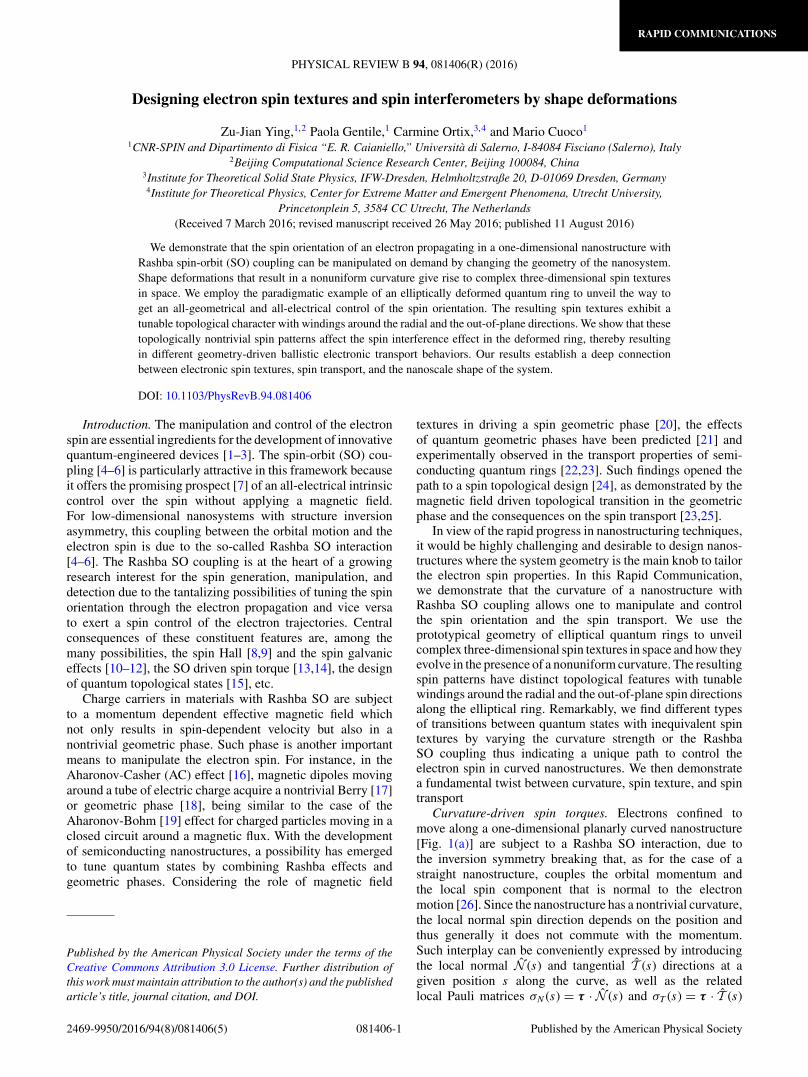
FIG. 1. Schematics of (a) the profile of a planarly curvednanowire and (b) the related curvature K(s). (c) denotes the Frenet-Serret-Bloch sphere in the moving frame of the electrons with thevectors associated to the electron spin orientation and the effectivefield heff.
in the moving frame of the electrons, with τ being the usualPauli matrices [Fig. 1(a)]. Then, the Hamiltonian for a planarnonuniformly curved nanostructure with Rashba SO can bewritten as [26–29]
Hk·p = − �2
2m�∂2s + iαSO
2[σN (s)∂s + ∂sσN (s)], (1)
where s is the arclength of the planar curve measured from anarbitrary reference point, m� is the effective mass of the chargecarriers, and αSO is the Rashba SO coupling strength. Equa-tion (1) generalizes the Hamiltonian originally proposed fora quantum ring with constant curvature [30]. It is convenientto express the normal and tangential directions to the curve interms of a polar angle f (s) as N (s) = {cos f (s), sin f (s),0},and T (s) = {sin f (s), − cos f (s),0}. Using the Frenet-Serret(FS) type equation of motion [31], ∂sN (s) = K(s)T (s), whereK(s) is the local curvature, we can immediately relate the polarangle to the local curvature via ∂sf (s) = −K(s) [Figs. 1(a)and 1(b)]. To proceed further, we use the fact that a spineigenmode |�E〉 of the Hamiltonian in Eq. (1) evolvesin space according to i∂s |�E〉 = G(s)|�E〉 where G(s) =−[αRσN (s) + c0 σ0], αR = m∗αSO
�2 being the inverse Rashba SOlength, while c2
0 = 2m∗E�2 + α2
R depends upon the eigenergyE. This relation allows us to derive the spin torque exertedon the electron spin through a fundamental equation thatlinks the geometric curvature of the nanostructure, the RashbaSO coupling, and the electron spin orientation in the FSframe [32]:
∂s〈σ 〉 = heff × 〈σ 〉. (2)
Here, the local spin orientation is 〈σ 〉 = {〈σT 〉,〈σN 〉,〈σz〉}while the effective spin-orbit field heff = {0,−2αR,K(s)}lies in the normal-binormal plane and depends on the localcurvature and αR . The spin direction then defines a Frenet-Serret-Bloch (FSB) sphere which is expressed in terms ofthe azimuthal and polar angles θ (s) and ϕ(s) [Fig. 1(c)].Equation (2) generally implies that due to a nonzero curvature,the electron spin acquires a finite out-of-plane binormal z
component. More importantly, a nontrivial component alongthe tangential direction appears provided the curvature is not
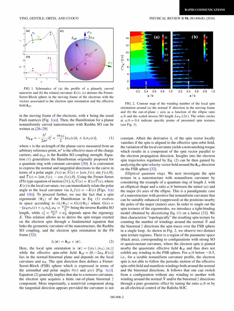
FIG. 2. Contour map of the winding number of the local spinorientation around (a) the normal N direction in the moving frameand (b) the out-of-plane z axis as a function of the ellipse ratioa/b and the scaled inverse SO length LαR/(2π ). The white circlesat a/b = 0.4 indicate specific points of presented spin textures(see Fig. 3).
constant. Albeit the derivative ∂s of the spin vector locallyvanishes if the spin is aligned to the effective spin-orbit field,the variation of the local curvature yields a nonvanishing torquewhich results in a component of the spin vector parallel tothe electron propagation direction. Insights into the electronspin trajectories regulated by Eq. (2) can be then gained byanalyzing the spin velocity vector field around the heff directionon the FSB sphere [32].
Elliptical quantum rings. We next investigate the spintexture in a nanostructure with nonuniform curvature byconsidering the example of a quantum ring of length L withan elliptical shape and a ratio a/b between the minor (a) andthe major (b) axes of the ellipse. This is a paradigmatic caseof a nanostructure with positive but nonuniform curvature thatcan be suitably enhanced (suppressed) at the positions nearbythe poles of the major (minor) axes. In order to single out thespin textures of the eigenmodes, we introduce a tight-bindingmodel obtained by discretizing Eq. (1) on a lattice [32]. Wethen characterize “topologically” the resulting spin texture bycounting the number of windings around the normal N andthe binormal z directions the spin traces over the FSB spherein a single loop. As shown in Fig. 2, we observe two distinctspin texture regimes. There is a region of the parameter space(black area), corresponding to configurations with strong SOor quasiconstant curvature, where the electron spin is pinnednearby the quasistatic effective field heff and thus does notexhibit any winding in the FSB sphere. For a/b below ∼0.5,i.e., for a sizable nonuniform curvature profile, the electronspin is not able to follow the periodic motion of the effectivespin-orbit field and manifests windings both around the normaland the binormal directions. It follows that one can switchfrom a configuration without any winding to another withwinding around the normal N and/or the binormal z directionsthrough a pure geometric effect by tuning the ratio a/b or byan all-electrical control of the Rahsba SOC.
081406-2
RAPID COMMUNICATIONS
DESIGNING ELECTRON SPIN TEXTURES AND SPIN . . . PHYSICAL REVIEW B 94, 081406(R) (2016)
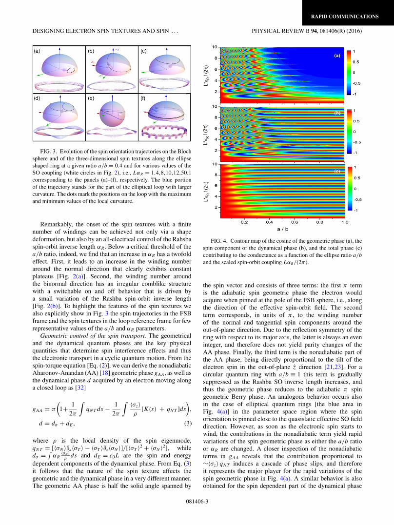
FIG. 3. Evolution of the spin orientation trajectories on the Blochsphere and of the three-dimensional spin textures along the ellipseshaped ring at a given ratio a/b = 0.4 and for various values of theSO coupling (white circles in Fig. 2), i.e., LαR = 1,4,8,10,12,50.1corresponding to the panels (a)–(f), respectively. The blue portionof the trajectory stands for the part of the elliptical loop with largercurvature. The dots mark the positions on the loop with the maximumand minimum values of the local curvature.
Remarkably, the onset of the spin textures with a finitenumber of windings can be achieved not only via a shapedeformation, but also by an all-electrical control of the Rahsbaspin-orbit inverse length αR . Below a critical threshold of thea/b ratio, indeed, we find that an increase in αR has a twofoldeffect. First, it leads to an increase in the winding numberaround the normal direction that clearly exhibits constantplateaus [Fig. 2(a)]. Second, the winding number aroundthe binormal direction has an irregular comblike structurewith a switchable on and off behavior that is driven bya small variation of the Rashba spin-orbit inverse length[Fig. 2(b)]. To highlight the features of the spin textures wealso explicitly show in Fig. 3 the spin trajectories in the FSBframe and the spin textures in the loop reference frame for fewrepresentative values of the a/b and αR parameters.
Geometric control of the spin transport. The geometricaland the dynamical quantum phases are the key physicalquantities that determine spin interference effects and thusthe electronic transport in a cyclic quantum motion. From thespin-torque equation [Eq. (2)], we can derive the nonadiabaticAharonov-Anandan (AA) [18] geometric phase gAA, as well asthe dynamical phase d acquired by an electron moving alonga closed loop as [32]
gAA = π
(1+ 1
2π
∫qNT ds − 1
2π
∫ 〈σz〉ρ
[K(s) + qNT ]ds
),
d = dσ + dE, (3)
where ρ is the local density of the spin eigenmode,qNT = [〈σN 〉∂s〈σT 〉 − 〈σT 〉∂s〈σN 〉]/[〈σT 〉2 + 〈σN 〉2], whiledσ = ∫
αR〈σN 〉
ρds and dE = c0L are the spin and energy
dependent components of the dynamical phase. From Eq. (3)it follows that the nature of the spin texture affects thegeometric and the dynamical phase in a very different manner.The geometric AA phase is half the solid angle spanned by
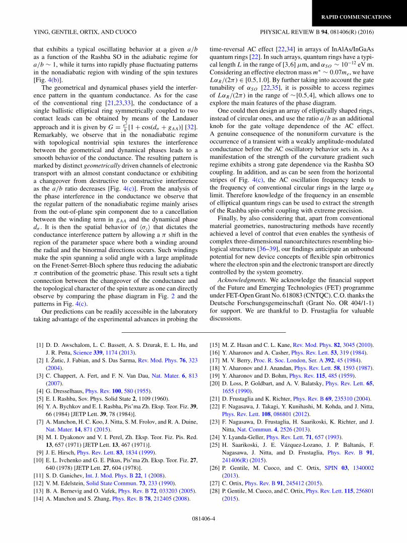
FIG. 4. Contour map of the cosine of the geometric phase (a), thespin component of the dynamical phase (b), and the total phase (c)contributing to the conductance as a function of the ellipse ratio a/b
and the scaled spin-orbit coupling LαR/(2π ).
the spin vector and consists of three terms: the first π termis the adiabatic spin geometric phase the electron wouldacquire when pinned at the pole of the FSB sphere, i.e., alongthe direction of the effective spin-orbit field. The secondterm corresponds, in units of π , to the winding numberof the normal and tangential spin components around theout-of-plane direction. Due to the reflection symmetry of thering with respect to its major axis, the latter is always an eveninteger, and therefore does not yield parity changes of theAA phase. Finally, the third term is the nonadiabatic part ofthe AA phase, being directly proportional to the tilt of theelectron spin in the out-of-plane z direction [21,23]. For acircular quantum ring with a/b ≡ 1 this term is graduallysuppressed as the Rashba SO inverse length increases, andthus the geometric phase reduces to the adiabatic π spingeometric Berry phase. An analogous behavior occurs alsoin the case of elliptical quantum rings [the blue area inFig. 4(a)] in the parameter space region where the spinorientation is pinned close to the quasistatic effective SO fielddirection. However, as soon as the electronic spin starts towind, the contributions in the nonadiabatic term yield rapidvariations of the spin geometric phase as either the a/b ratioor αR are changed. A closer inspection of the nonadiabaticterms in gAA reveals that the contribution proportional to∼〈σz〉 qNT induces a cascade of phase slips, and thereforeit represents the major player for the rapid variations of thespin geometric phase in Fig. 4(a). A similar behavior is alsoobtained for the spin dependent part of the dynamical phase
081406-3
RAPID COMMUNICATIONS
YING, GENTILE, ORTIX, AND CUOCO PHYSICAL REVIEW B 94, 081406(R) (2016)
that exhibits a typical oscillating behavior at a given a/b
as a function of the Rashba SO in the adiabatic regime fora/b ∼ 1, while it turns into rapidly phase fluctuating patternsin the nonadiabatic region with winding of the spin textures[Fig. 4(b)].
The geometrical and dynamical phases yield the interfer-ence pattern in the quantum conductance. As for the caseof the conventional ring [21,23,33], the conductance of asingle ballistic elliptical ring symmetrically coupled to twocontact leads can be obtained by means of the Landauerapproach and it is given by G = e2
h[1 + cos(dσ + gAA)] [32].
Remarkably, we observe that in the nonadiabatic regimewith topological nontrivial spin textures the interferencebetween the geometrical and dynamical phases leads to asmooth behavior of the conductance. The resulting pattern ismarked by distinct geometrically driven channels of electronictransport with an almost constant conductance or exhibitinga changeover from destructive to constructive interferenceas the a/b ratio decreases [Fig. 4(c)]. From the analysis ofthe phase interference in the conductance we observe thatthe regular pattern of the nonadiabatic regime mainly arisesfrom the out-of-plane spin component due to a cancellationbetween the winding term in gAA and the dynamical phasedσ . It is then the spatial behavior of 〈σz〉 that dictates theconductance interference pattern by allowing a π shift in theregion of the parameter space where both a winding aroundthe radial and the binormal directions occurs. Such windingsmake the spin spanning a solid angle with a large amplitudeon the Frenet-Serret-Bloch sphere thus reducing the adiabaticπ contribution of the geometric phase. This result sets a tightconnection between the changeover of the conductance andthe topological character of the spin texture as one can directlyobserve by comparing the phase diagram in Fig. 2 and thepatterns in Fig. 4(c).
Our predictions can be readily accessible in the laboratorytaking advantage of the experimental advances in probing the
time-reversal AC effect [22,34] in arrays of InAlAs/InGaAsquantum rings [22]. In such arrays, quantum rings have a typi-cal length L in the range of [3,6] μm, and αSO ∼ 10−12 eV m.Considering an effective electron mass m∗ ∼ 0.07me, we haveLαR/(2π ) ∈ [0.5,1.0]. By further taking into account the gatetunability of αSO [22,35], it is possible to access regimesof LαR/(2π ) in the range of ∼ [0.5,4], which allows one toexplore the main features of the phase diagram.
One could then design an array of elliptically shaped rings,instead of circular ones, and use the ratio a/b as an additionalknob for the gate voltage dependence of the AC effect.A genuine consequence of the nonuniform curvature is theoccurrence of a transient with a weakly amplitude-modulatedconductance before the AC oscillatory behavior sets in. As amanifestation of the strength of the curvature gradient suchregime exhibits a strong gate dependence via the Rashba SOcoupling. In addition, and as can be seen from the horizontalstripes of Fig. 4(c), the AC oscillation frequency tends tothe frequency of conventional circular rings in the large αR
limit. Therefore knowledge of the frequency in an ensembleof elliptical quantum rings can be used to extract the strengthof the Rashba spin-orbit coupling with extreme precision.
Finally, by also considering that, apart from conventionalmaterial geometries, nanostructuring methods have recentlyachieved a level of control that even enables the synthesis ofcomplex three-dimensional nanoarchitectures resembling bio-logical structures [36–39], our findings anticipate an unboundpotential for new device concepts of flexible spin orbitronicswhere the electron spin and the electronic transport are directlycontrolled by the system geometry.
Acknowledgments. We acknowledge the financial supportof the Future and Emerging Technologies (FET) programmeunder FET-Open Grant No. 618083 (CNTQC). C.O. thanks theDeutsche Forschungsgemeinschaft (Grant No. OR 404/1-1)for support. We are thankful to D. Frustaglia for valuablediscussions.
[1] D. D. Awschalom, L. C. Bassett, A. S. Dzurak, E. L. Hu, andJ. R. Petta, Science 339, 1174 (2013).
[2] I. Zutic, J. Fabian, and S. Das Sarma, Rev. Mod. Phys. 76, 323(2004).
[3] C. Chappert, A. Fert, and F. N. Van Dau, Nat. Mater. 6, 813(2007).
[4] G. Dresselhaus, Phys. Rev. 100, 580 (1955).[5] E. I. Rashba, Sov. Phys. Solid State 2, 1109 (1960).[6] Y. A. Bychkov and E. I. Rasbha, Pis’ma Zh. Eksp. Teor. Fiz. 39,
66 (1984) [JETP Lett. 39, 78 (1984)].[7] A. Manchon, H. C. Koo, J. Nitta, S. M. Frolov, and R. A. Duine,
Nat. Mater. 14, 871 (2015).[8] M. I. Dyakonov and V. I. Perel, Zh. Eksp. Teor. Fiz. Pis. Red.
13, 657 (1971) [JETP Lett. 13, 467 (1971)].[9] J. E. Hirsch, Phys. Rev. Lett. 83, 1834 (1999).
[10] E. L. Ivchenko and G. E. Pikus, Pis’ma Zh. Eksp. Teor. Fiz. 27,640 (1978) [JETP Lett. 27, 604 (1978)].
[11] S. D. Ganichev, Int. J. Mod. Phys. B 22, 1 (2008).[12] V. M. Edelstein, Solid State Commun. 73, 233 (1990).[13] B. A. Bernevig and O. Vafek, Phys. Rev. B 72, 033203 (2005).[14] A. Manchon and S. Zhang, Phys. Rev. B 78, 212405 (2008).
[15] M. Z. Hasan and C. L. Kane, Rev. Mod. Phys. 82, 3045 (2010).[16] Y. Aharonov and A. Casher, Phys. Rev. Lett. 53, 319 (1984).[17] M. V. Berry, Proc. R. Soc. London, Ser. A 392, 45 (1984).[18] Y. Aharonov and J. Anandan, Phys. Rev. Lett. 58, 1593 (1987).[19] Y. Aharonov and D. Bohm, Phys. Rev. 115, 485 (1959).[20] D. Loss, P. Goldbart, and A. V. Balatsky, Phys. Rev. Lett. 65,
1655 (1990).[21] D. Frustaglia and K. Richter, Phys. Rev. B 69, 235310 (2004).[22] F. Nagasawa, J. Takagi, Y. Kunihashi, M. Kohda, and J. Nitta,
Phys. Rev. Lett. 108, 086801 (2012).[23] F. Nagasawa, D. Frustaglia, H. Saarikoski, K. Richter, and J.
Nitta, Nat. Commun. 4, 2526 (2013).[24] Y. Lyanda-Geller, Phys. Rev. Lett. 71, 657 (1993).[25] H. Saarikoski, J. E. Vazquez-Lozano, J. P. Baltanas, F.
Nagasawa, J. Nitta, and D. Frustaglia, Phys. Rev. B 91,241406(R) (2015).
[26] P. Gentile, M. Cuoco, and C. Ortix, SPIN 03, 1340002(2013).
[27] C. Ortix, Phys. Rev. B 91, 245412 (2015).[28] P. Gentile, M. Cuoco, and C. Ortix, Phys. Rev. Lett. 115, 256801
(2015).
081406-4
RAPID COMMUNICATIONS
DESIGNING ELECTRON SPIN TEXTURES AND SPIN . . . PHYSICAL REVIEW B 94, 081406(R) (2016)
[29] E. Zhang, S. Zhang, and Q. Wang, Phys. Rev. B 75, 085308(2007).
[30] F. E. Meijer, A. F. Morpurgo, and T. M. Klapwijk, Phys. Rev. B66, 033107 (2002).
[31] R. Dandoloff, R. Balakrishnan, and A. R. Bishop, J. Phys. A:Math. Gen. 25, L1105 (1992).
[32] See Supplemental Material at http://link.aps.org/supplemental/10.1103/PhysRevB.94.081406 for the derivation of thegyroscope-like equation for the spatial evolution of the local spinorientation in a generic planarly curved nanowire with Rashbaspin-orbit coupling. We demonstrate how the spin velocityvector field behaves around the positions corresponding to thelocally vanishing effective spin-orbit torque. Then, we derivethe expression for the geometric phase acquired by an electrongoing around a loop having a nontrivial geometric curvatureand Rashba spin-orbit coupling. We derive the expression forthe quantum conductance of an elliptical ring symmetrically
coupled to two contact leads. Finally, we provide the detailsfor the continuum-to-lattice mapping of the Hamiltonian for acurved nanowire and the methodology applied to determine thephase diagrams.
[33] D. Bercioux, D. Frustaglia, and M. Governale, Phys. Rev. B 72,113310 (2005).
[34] C. P. Umbach, C. Van Haesendonck, R. B. Laibowitz, S.Washburn, and R. A. Webb, Phys. Rev. Lett. 56, 386 (1986).
[35] D. Liang and X. P. A. Gao, Nano Lett. 12, 3263 (2012).[36] V. Y. Prinz, V. A. Seleznev, A. K. Gutakovsky, A. V. Chehovskiy,
V. V. Preobrazhenskii, M. A. Putyato, and T. A. Gavrilova,Physica E (Amsterdam) 6, 828 (2000).
[37] O. G. Schmidt and K. Eberl, Nature (London) 410, 168(2001).
[38] H.-F. Zhang, C.-M. Wang, and L.-S. Wang, Nano Lett. 2, 941(2002).
[39] S. Xu, Z. Yan, K.-I. Jang et al., Science 347, 154 (2015).
081406-5
Related Documents