Design Methodology for Shunt Active Filters Fabio Ronchi, Andrea Tilli Department of Electronics, Computer and System Sciences (DEIS), University of Bologna Viale Risorgimento 2, 40136 Bologna, ITALY phone: +39 051 2093069, fax: +39 051 2093073 e-mail: fronchi, atilli @deis.unibo.it Keywords Active filter, design, harmonics, three-phase systems. Abstract This artic le deals with the design of a thre e-wi re shunt acti ve filter based on a AC/DC con ver ter. A methodolo gy to select suitable values of the components is presented for two design objectives. The first one is to select components val ues str ictly dep enda nt on the le vel of curr ent dist orti on imposed by th e load. The secon d goal is to find the mini mum capacitor value necessary to compensate all the possible loads compatible with a specific current size of the switches. Both the algorithms are based on a model inversion and are control-oriented. Introduction Nonlinear loads produce current harmonics that pollute the network mains and can disturb all the devices expected to work with sinusoi dal volt ages and curr ents. This fact increa ses costs and reduces perfor mances for both ener gy consumers and providers. Several schemes and control techniques have been proposed in the past years, often assuming that all the components are well size d, or at least that they do not aff ect the control algor ithm perfor mance [1], [2], [3], [4]. The first step in design ing an active filter is to sele ct suitabl e compon ents value s. This allo ws to redu ce costs and avoids a lot of control probl ems. The aim of this paper is to present an algorith m to properl y sele ct the hard ware compo nents of a very simple and usual scheme of shunt active filte r. The first design metho dology prese nted is based on the kno wledg e of the harmonic spectr um of the load current s. It allows to sele ct the minimu m hard ware compo nents values that make the filter capabl e to compensa te for the distorte d curr ents. The second design algorit hm is relate d to the peak curre nt of the bridge switche s. It permits to find the minimum hardware componen t val ues that make the filter capable to compensate for all the loads which have distorted currents smaller than the maximum currents allowed for the switches . Both the desig n proc edur es can be iter ated to impro ve perfor mance s, for exampl e consi deri ng if a higher sample frequency and a higher capacitor voltage can be chosen. In the first paragra ph some hypothe sis and basi c desi gn consider atio ns are prese nted. In the second one the model of the shunt active filt er is shown . In the thir d one the choi ce of the inductance va lue is discu sse d. The other two paragraphs present the two design methodologies, the first one is indicated as “load-based”, the second one as “switches-based”. Conclusions summarize the contents of the article. 1 Pr el iminaries In this section some definitions, assumptions and preliminary design considerations are presented.

Welcome message from author
This document is posted to help you gain knowledge. Please leave a comment to let me know what you think about it! Share it to your friends and learn new things together.
Transcript
5/7/2018 Design Methodology for Shunt Active Filters - slidepdf.com
http://slidepdf.com/reader/full/design-methodology-for-shunt-active-filters 1/8
Design Methodology for Shunt Active Filters
Fabio Ronchi, Andrea Tilli
Department of Electronics, Computer and System Sciences (DEIS),
University of Bologna
Viale Risorgimento 2,
40136 Bologna, ITALY
phone: +39 051 2093069, fax: +39 051 2093073
e-mail:
fronchi, atilli ¡ @deis.unibo.it
Keywords
Active filter, design, harmonics, three-phase systems.
Abstract
This article deals with the design of a three-wire shunt active filter based on a AC/DC converter. A methodology to
select suitable values of the components is presented for two design objectives. The first one is to select components
values strictly dependant on the level of current distortion imposed by the load. The second goal is to find the minimum
capacitor value necessary to compensate all the possible loads compatible with a specific current size of the switches.
Both the algorithms are based on a model inversion and are control-oriented.
Introduction
Nonlinear loads produce current harmonics that pollute the network mains and can disturb all the devices expected
to work with sinusoidal voltages and currents. This fact increases costs and reduces performances for both energy
consumers and providers.
Several schemes and control techniques have been proposed in the past years, often assuming that all the components
are well sized, or at least that they do not affect the control algorithm performance [1], [2], [3], [4]. The first step
in designing an active filter is to select suitable components values. This allows to reduce costs and avoids a lot
of control problems. The aim of this paper is to present an algorithm to properly select the hardware components
of a very simple and usual scheme of shunt active filter. The first design methodology presented is based on the
knowledge of the harmonic spectrum of the load currents. It allows to select the minimum hardware components
values that make the filter capable to compensate for the distorted currents. The second design algorithm is relatedto the peak current of the bridge switches. It permits to find the minimum hardware component values that make the
filter capable to compensate for all the loads which have distorted currents smaller than the maximum currents allowed
for the switches. Both the design procedures can be iterated to improve performances, for example considering if a
higher sample frequency and a higher capacitor voltage can be chosen.
In the first paragraph some hypothesis and basic design considerations are presented. In the second one the model
of the shunt active filter is shown. In the third one the choice of the inductance value is discussed. The other
two paragraphs present the two design methodologies, the first one is indicated as “load-based”, the second one as
“switches-based”. Conclusions summarize the contents of the article.
1 Preliminaries
In this section some definitions, assumptions and preliminary design considerations are presented.
5/7/2018 Design Methodology for Shunt Active Filters - slidepdf.com
http://slidepdf.com/reader/full/design-methodology-for-shunt-active-filters 2/8
L L L
N
K
C
LOAD
¢¤ £¦ ¥
¢£¦ §
¢¨ £¦ ©
£ ¥
£¦ §
£¦ ©
¥
§
©
¥
§
©
¢
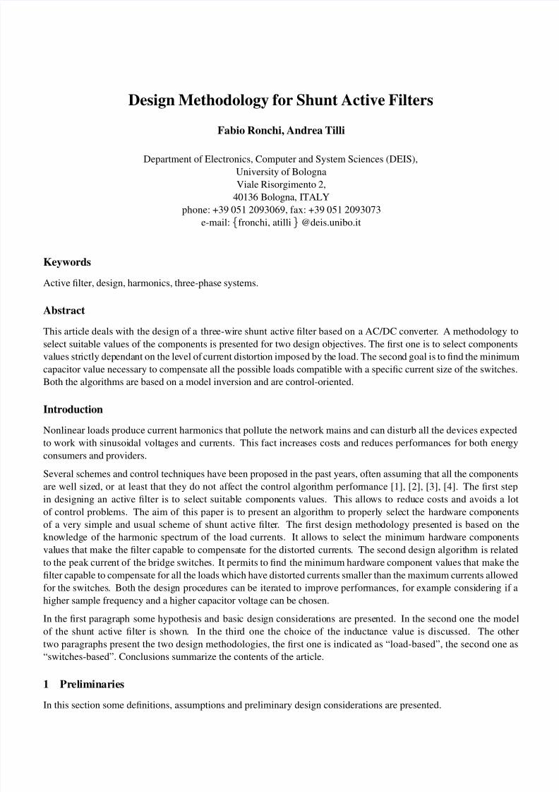
Figure 1: Shunt active filter scheme
1. The scheme of the active filter considered in this article is presented in Fig. 1. It is a three-phase AC/DC
converter, where the capacitor is the main energy storage element and the inductors are used for the control
of the filter currents by means of the converter voltages. In Fig. 1: ¦ !# "$
¦ %
"& '
are the mains voltages,(
¦ ! "
(
¦ %
"
(
¦ ' are the mains currents,
(0 )
!"
( )
%"
( )
'are the load currents,
# 1is the capacitor voltage (DC BUS).
2. The mains voltages ¦ !3 2 5 4 7 68 "9
%
2 5 47 68 "9 ¦ '@ 2 5 4A 6
are co-sinusoidal of frequency BC D 2 F E ¨ GI HQ P
or R¨ GS HT PU 6
, balanced
and equilibrated.
¨ !V 2 5 4A 6X W Ya c be dC fF 2 h g ip B¤ & 47 6
%
25 47 6X Wq Yr s be dC f
t
g¨ ip B¤ $ 4v u
g¨ i
wy x
¨ '@ 2 5 4 7 6X W� u� � ¦ !3 2 5 47 6p �� % 2 5 47 6 �
3. The sampling frequencyB# �
and the PWM frequencyBC �p �� �
are supposed already chosen.
4. The load currents(� )
!"
( )
%"
( )
'are balanced and periodic of frequency B
C :
( )� �
2 5 4A 69 W� �
)� � �
�
�
�
� �F
�
)� �
� e
2 h g ip ja B¤ k 4l �n m
�
�
6 " o W� " "
where M is equal to infinity according to the Fourier analysis. However, only a reduced number of harmonics
is considered for the compensation, owing to limited bandwidth of the controlled inverter.
5. Inductors are modelled as pure inductances L.
6. The six-switches-bridge is supposed ideal.
7. The maximum current of the devices implementing the bridge switches is �#
¦ !7
. It is worth underlining that
several shunt active filters can be parallel connected to the same load, providing a suitable coordinating strategy
to increase the compensated current.
8. The steady-state capacitor voltage must be kept inside the range �� Yp 9 z { "v Yr !7 � . The upper bound Y
!7 depends
on the kind of capacitor chosen and on the number of series connected capacitor banks. Hence, it can be
assumed chosen before starting the design procedure. The lower bound Yp |
depends on the controllability
constraints, as explained in section 4.
9. The shunt active filter has to produce currents opposite to the load distorted ones. It will be assumed that thecontrol techniques implemented are able to assure this behavior.

5/7/2018 Design Methodology for Shunt Active Filters - slidepdf.com
http://slidepdf.com/reader/full/design-methodology-for-shunt-active-filters 3/8
-0.8 -0.6 -0.4 -0.2 0 0.2 0.4 0.6 0.8
-0.6
-0.4
-0.2
0
0.2
0.4
0.6
a
b
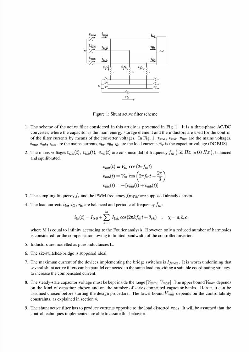
c
Figure 2: Hexagon of feasible }!8 %h '
2 Shunt active filter model
Let ¨ ~ 2 5 4A 6y W � ¤ ¦ !V 2 5 4 7 68 "A
%
2 5 47 68 "A ' 2 5 47 6 � ,
(
r 2 5 47 6 W �
(
!
2 5 47 68 "
(
%
2 5 47 68 "
(
'
2 5 47 6 � ,
C @ ~ 2 5 4A 6 W � 2 5 47 68 "A C e 2 5 47 68 "A C � ~ 2 5 4A 6 � ,
}�
� 2
5 4A 6X W� � }� r 2 5 47 68 "A }
2 5 47 68 "A }
�2 5 4A 6 �
be the arrays of, respectively: mains voltages, filter currents, voltages from the node
K to the half points of bridge legs, control inputs of the six-switches-bridge,}
�� �
G "@ �¤ ¡C "v o Wq � " "
. Then the filter
equations can be written, starting from inductor dynamics
2 5 47 6 W
2 5 47 6v u
(
r 2 5 47 6
4
W }
8 � 2 5 47 6{ 1¤ 2 5 4 7 6v u
¦ 2
5 47 6¦ I � � �
From the sum of the three scalar equations above, it can be found that
¦
25 4A 69 W
}� r 2 5 4 7 6l �� }
2 5 4A 6l �� }
�2 5 4A 6
w 1 2 5 4 A 6
that permits to define
}! %h '
2 5 47 6X W }�
� 2
5 4A 6� u
}� r 2 5 4A 6� �� }
2 5 47 6p �� }
�2 5 4A 6
w
� � � �
}!8 %h '
can assume only 7 values at the time 48 �
, which correspond to the vertexes of the hexagon of Fig. 2. The region
included in this hexagon corresponds to the }! %h '
that can be obtained as mean values in a PWM period. The status
equations of the filter are:
(
r 2 5 4A 6
4
W 2 5 4A 6� u } !
8 %h '
2 5 4A 6{ 1
2 5 4A 6 (1)
�
1
2 5 4A 6
4
W }
!8 %h '
2 5 4A 6
(
r 2 5 4 A 6
(2)
It is useful to write the model also in a d-q reference frame, aligned to the mains voltage vector. In this frame mainsvoltages and load currents can be written as
�7
¤ � W
w
g
Yr �
�
G
W
Y
�
�
G
�7
( )
2 5 47 6X W
( )
�
2 5 4A 6
( )
25 47 6
W
�
)
�
�
�
( )
�7
25 4A 6
( )
2 5 4A 6
(3)
and the status equations (1), (2) become
�
(
a 2 5 4A 6
4
Wq g ip B¤
G �
uS � G
�7
(
a 2 5 4 7 6p �
�
�7
¨ ª u
¨ 1 2 5 47 6
�7
}!8 %h '
2 5 47 6
1
2 5 47 6
4
W
�
�¬ «
�7
}!8 %h '
2 5 47 6
�7
(
a 2 5 4 7 6

5/7/2018 Design Methodology for Shunt Active Filters - slidepdf.com
http://slidepdf.com/reader/full/design-methodology-for-shunt-active-filters 4/8
0 0..1 0..2 0..3 0..4 0..5 0..6 0..7 0..8
0
0..1
0..2
0..3
0..4
0..5 1U
U2
Uabc*
Figure 3: current ripple worst case
3 Minimum value of inductance
The minimum value of inductance is calculated in a way that does not depends on the loads, so that it is the same for
both the design objectives and can be previously calculated.
The use of PWM techniques to obtain the reference values }F �
!8 %h '
causes current ripple, that must be kept less than a
maximum value ® � �° 7 ¯
in order to bound high frequency distortion.
(
a 2 5 4A 6X W
(
�
2 5 47 6p �± ®
(
a 2 5 47 6
}! %h '
25 47 6X W }
�
! %h '
2 5 47 6p �± ®~ } !
%h '
2 5 47 6
where the � indicates reference value and ® the ripple caused by the PWM technique. Substituting these expressions
in the status equations (1), (2) it will be obtained that
®
(
� 2 5 4 A 6
4
W² uk ®~ } !
8 %h '
2 5 4A 6 1
2 5 47 6
The ripple worst case is }l �
!8 %h '
in the middle of an hexagon side, as illustrated in Fig. 3. In this situation the peak to
peak current ripple is, assuming that the capacitor voltage Yp 1
is constant in a PWM-period,
® � ¯
7 ¯
Wq ³n ¶ µ7 ·
� ¹0 º
´¶ µ
e
®
(
� 2 5 4 A 6
4
� » ¼
4 W
Y1
RI � B �
p �� �
It must be less than the maximum ripple chosen ® � �
° 7 ¯
® � ¯
7 � ½
® � �
° 7 ¯
Wp ¾ 9 9 z W
Y ¦ !7
R¿ B �
p �� �
® � �
° 7 ¯
(4)
For instance, if Y� ¦ !7 Wq À E GI Y
, B�p �� �
W� g G¿ j HQ P
, ® � �
° 7 ¯
WÁ gk Â
, then must be greater thanwV Ã
�@ gk Ä H
4 Load-based approach
Currents that have to be compensated can be written as in (3). In order to reach an unitary power factor, the only load
current component that the filter must not compensate for is �
)
�
�
because
Å
)
2 5 4A 69 W
«
�7
¨
�
( )
2 5 4A 69 Wq Y
�
�
�
)
�
�
�Æ Y
�
�e ( )
�7
2 5 4A 6 (5)
Therefore the filter currents that should be tracked are(
�
2 5 4A 6 W
(
�
�
2 5 47 68 "
(
�
2 5 47 6
W
u
( )
�7
2 5 4A 68 " u
( )
2 5 47 6
5/7/2018 Design Methodology for Shunt Active Filters - slidepdf.com
http://slidepdf.com/reader/full/design-methodology-for-shunt-active-filters 5/8
-200 -150 -100 -50 0 50 100 150 200
-150
-100
-50
0
50
100
150
a
b
c
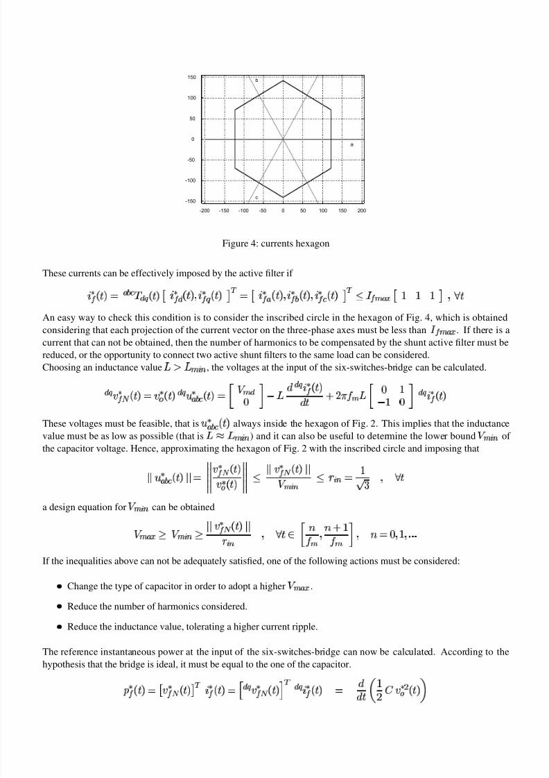
Figure 4: currents hexagon
These currents can be effectively imposed by the active filter if
(
�
25 47 6X W
! %h '0 Ç
�7
2 5 4A 6¦
(
�
�
25 47 68 "
(
�
25 47 6
WÈ
(
�
!
2 5 4A 68 "
(
�
%
2 5 4A 68 "
(
�
'
2 5 47 6
� É
�@ ! ° � � � y "p Ê 4
An easy way to check this condition is to consider the inscribed circle in the hexagon of Fig. 4, which is obtained
considering that each projection of the current vector on the three-phase axes must be less than �3 !7
. If there is a
current that can not be obtained, then the number of harmonics to be compensated by the shunt active filter must be
reduced, or the opportunity to connect two active shunt filters to the same load can be considered.
Choosing an inductance value ª ˪ Ì 9 z
, the voltages at the input of the six-switches-bridge can be calculated.
�7
�
@
2 5 4A 6X W�
�
1
2 5 47 6
�7
}
�
!8 %h '
2 5 47 6X W
Y
�
G
u
�7
(
�
2 5 4A 6
4
�Æ g ip B¤ k
G �
uS �Í G
�7
(
�
2 5 47 6
These voltages must be feasible, that is }F �
! %h '
2 5 47 6
always inside the hexagon of Fig. 2. This implies that the inductance
value must be as low as possible (that is Î Ì 9 z ) and it can also be useful to determine the lower bound Y
Ï | of
the capacitor voltage. Hence, approximating the hexagon of Fig. 2 with the inscribed circle and imposing that
Ð
}
�
!8 %h '
25 4A 6
Ð
WÍ Ñ
Ñ
Ñ
Ñ
Ñ
�
@
25 47 6
�1
2 5 4A 6
Ñ
Ñ
Ñ
Ñ
Ñ
É
Ð
�
2 5 47 6
Ð
Ya |
ÉÓ Ò
z W
�
Ô
w
"Õ Ê 4
a design equation for Y 9 z can be obtained
Ya ¦ !7 Ö× Yr 9 z Ø Ö
Ð
V �
25 47 6
Ð
Ò
z
"Í Ê{ 4
�
& Ù
B¤
" Ù
�� �
B¤
"
Ù
WÁ G "@ � "
à à Ã
If the inequalities above can not be adequately satisfied, one of the following actions must be considered:
Ú Change the type of capacitor in order to adopt a higher YÏ ¦ !7 .
Ú Reduce the number of harmonics considered.
Ú Reduce the inductance value, tolerating a higher current ripple.
The reference instantaneous power at the input of the six-switches-bridge can now be calculated. According to the
hypothesis that the bridge is ideal, it must be equal to the one of the capacitor.
Å
�
25 47 6 WÈ Û
�
2 5 47 6
(
�
2 5 47 6 W
«
�7
�
@
2 5 47 6
�7
(
�
2 5 47 6 W
4
t
�
g
�
�º
1
2 5 47 6 x
5/7/2018 Design Methodology for Shunt Active Filters - slidepdf.com
http://slidepdf.com/reader/full/design-methodology-for-shunt-active-filters 6/8
This equation can be used to choose the capacitor value. The energy
Ü
�
2 5 47 6X Wq ³� ´
´¶ µ
Å
�
2 Þ Ý� 6
Ý
is periodic of frequencyB
by hypothesis and its mean value is zero. DefiningÜ
¦ !7 W
� ß à¤ á
´ â
Ü
�
2 5 4A 6
â
Ya ãA ä0 I W
Y !7 �
ª Y
|
g
and imposing that the related voltage variation is 2 å Yl ã0 ä0 v uæ Y 9 z 6
, it can be obtained the capacitor value design equation
�
W
g
Ü
¦ !7
Y
º
ã0 ä0
u� Y
º
9 z
An interesting example of application of this methodology is the following. Considering a six pulse diode bridge
rectifier with a resistance of w� ç
as load; assuming è Wé � � "7 ê W �
Ãë w
Ä HQ "7 �
!7
Wì À Eí Â "8 Yr ã0 ä0 � W× î G GQ Y , a
capacitance�
W² � G G� ïp ð
is obtained.
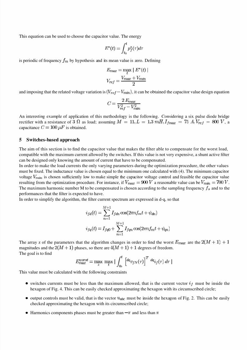
5 Switches-based approach
The aim of this section is to find the capacitor value that makes the filter able to compensate for the worst load,
compatible with the maximum current allowed by the switches. If this value is not very expensive, a shunt active filter
can be designed only knowing the amount of current that have to be compensated.
In order to make the load currents the only varying parameters during the optimization procedure, the other values
must be fixed. The inductance value is chosen equal to the minimum one calculated with (4). The minimum capacitor
voltage Yr z
is chosen sufficiently low to make simple the capacitor voltage control and feasible the capacitor value
resulting from the optimization procedure. For instance, if Yp !7 Wq ñ G G Y
a reasonable value can beY | Ø W� À¤ G GS Y
.The maximum harmonic number M to be compensated is chosen according to the sampling frequency B
� and to the
performances that the filter is expected to have.
In order to simplify the algorithm, the filter current spectrum are expressed in d-q, so that
(
�
2 5 47 6X W
�
·
�
�F
�@
�
be dC f 2 h g i
Ù
B¤ & 4l �� ò
�
6
(
2 5 4A 6X WÁ �@
�
�
�
·
�
�F
�@
be dC f 2 h g ¨ i
Ù
B¤ k 4l �n ò
a 6
The array z of the parameters that the algorithm changes in order to find the worst
Ü
!7
are thega 2 Þ è �� � 6Ì � �
magnitudes and the ga 2 Þ èé �� � 6
phases, so there are ó� 2 Þ è �� � 6p �� �
degrees of freedom.
The goal is to find
ÜS ô
1ã
�
´
!
WÁ ß à¤ á
�
ß à¤ á
´ â
³� ´
´¶ µ
«
�
C @ 2 Þ Ý� 6
�7
(
r 2 Þ Ý� 6
Ý
â
This value must be calculated with the following constraints
Ú switches currents must be less than the maximum allowed, that is the current vector(
must be inside the
hexagon of Fig. 4. This can be easily checked approximating the hexagon with its circumscribed circle;
Ú output controls must be valid, that is the vector }! %h '
must be inside the hexagon of Fig. 2. This can be easily
checked approximating the hexagon with its circumscribed circle;Ú Harmonics components phases must be greater than u
& iand less than i

5/7/2018 Design Methodology for Shunt Active Filters - slidepdf.com
http://slidepdf.com/reader/full/design-methodology-for-shunt-active-filters 7/8
0 0.002 0.004 0.006 0.008 0.01 0.012 0.014 0.016 0.018 0.02
-250
-200
-150
-100
-50
0
50
0 0.002 0.004 0.006 0.008 0.01 0.012 0.014 0.016 0.018 0.02
-3
-2
-1
0
1
2
3
x 104 Power Energy
Figure 5: Worst case power and worst case energy, 7 harmonics
This algorithm can be applied using the Matlab Optimization Toolbox (fmincon) [5], and the result is that the
worst Å
�
2 5 4A 6
is an approximately square wave.
For example, assuming z Wõ �
Ãë w
Ä H
, � ! Wö E GU Â
, Yr 9 z T W÷ À¤ G G Y
, Ya ãA ä0 � Wö î G G Y
and consideringè W÷ À
the worst power profileÅ
�
2 5 4A 6 and the related energy
Ü
�
2 5 47 6 are presented in Fig. 5. The resulting capacitor value
iswV Ã
gS Ä ð
. Increasing the number of harmonics considered, Å
�
25 47 6becomes more similar to a square wave, and the
related capacitor value increases, reachingwV Ã
ó° Ä ð
considering 16 harmonics.
6 Distorted mains voltages
If the mains voltages are distorted, then the capacitor has to provide more energy to the load and its value must be
bigger than the one calculated.
If the mains voltages are sinusoidal, balanced and equilibrated, then the load instant power is the one calculated in (5)
and the only power that the filter must deliver isY
�
� ( )
�7
25 47 6, which mean value is equal to zero.
If the mains voltages are distorted, then�7
¨ U 2 5 47 6 W Y
�
�
��
�7
25 47 68 "F
2 5 47 6
and load power becomes
Å
)
25 47 6 Wq Y
�
�
�
)
�
�
�Æ Y
�
�e ( )
�7
2 5 47 6l ��
�7
2 5 4A 6� �
)
�
�
�ê
�7
2 5 47 6
( )
�7
2 5 4A 6p �n ¤
2 5 47 6
( )
2 5 47 6
The above equation shows that the shunt active filter has to provide more power to the load, which mean value can
also be different from zero in a PWM period. Hence, also assuming that the power mean value becomes zero in a
larger time, the capacitor value must be increased in order to accumulate more energy.
Conclusions
Two design methodologies for an usual shunt active filter scheme have been presented.The first considers the particular load that has to be compensated and allows to find suitable values for the hardware
components of the filter.
The second one considers the peak current allowed by the bridge switches and finds the capacitor value that makes
the filter capable to compensate for all the loads compatible with the system constraints.
References
[1] S.Saadate J.H.XU, C.Lott and B.Davat. Simulation and Experimentation of a Voltage Source Active Filter Com-
pensating Current Harmonics and Power Factor . Ind. Electron., Control and Instrument., IECON’94, Volume 1:
Page(s) 411–415, 1994.
[2] Kamal Al-Haddad Bhim Singh and Ambrish Chandra. A Review of Active Filters for Power Quality Improvement .
IEEE Tran. on Ind. Electron., Volume 46: Pages 960–971, 1999.

5/7/2018 Design Methodology for Shunt Active Filters - slidepdf.com
http://slidepdf.com/reader/full/design-methodology-for-shunt-active-filters 8/8
[3] A.H.Noyola W.M.Grady, M.J.Samotyj. Survey of Active Power Line Conditioning Methodologies. IEEE Tran.
on Power Deliv., Volume 5: Page(s) 1536–1542, 1990.
[4] J.W.Dixon L.A.Moran, L.Fernandez and R.Wallace. A Simple and Low-Cost Control Strategy for Active Power
Filters Connected in Cascade. IEEE Tran. on Ind. Electron., Volume 44: Page(s) 621–629, 1997.
[5] A.Grace T.Coleman, M.A.Branch. Matlab Optimization Toolbox User’s Guide. The MathWorks Inc., 1999.
Related Documents