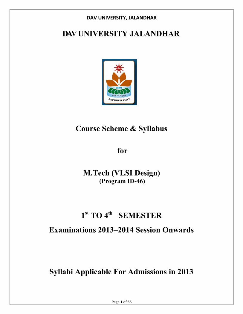
DAV UNIVERSITY, JALANDHAR DAV UNIVERSITY JALANDHAR Course Scheme & Syllabus for M.Tech (VLSI Design) (Program ID-46) 1 st TO 4 th SEMESTER Examinations 2013–2014 Session Onwards Syllabi Applicable For Admissions in 2013 Page 1 of 66

Welcome message from author
This document is posted to help you gain knowledge. Please leave a comment to let me know what you think about it! Share it to your friends and learn new things together.
Transcript
DAV UNIVERSITY, JALANDHAR
DAV UNIVERSITY JALANDHAR
Course Scheme & Syllabus
for
M.Tech (VLSI Design) (Program ID-46)
1st TO 4th SEMESTER
Examinations 2013–2014 Session Onwards
Syllabi Applicable For Admissions in 2013
Page 1 of 66
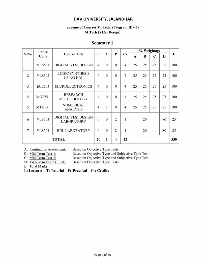
DAV UNIVERSITY, JALANDHAR
Scheme of Courses M. Tech. (Program ID-46) M.Tech (VLSI Design)
Semester 1
S.No Paper Code Course Title L T P Cr
% Weightage E A B C D
1 VLS501 DIGITAL VLSI DESIGN 4 0 0 4 25 25 25 25 100
2 VLS502 LOGIC SYNTHESIS USING HDL 4 0 0 4 25 25 25 25 100
3 ECE503 MICROELECTRONICS 4 0 0 4 25 25 25 25 100
4 MGT551 RESEARCH METHODOLOGY 4 0 0 4 25 25 25 25 100
5 MTH551 NUMERICAL ANALYSIS 4 1 0 4 25 25 25 25 100
6 VLS503 DIGITAL VLSI DESIGN LABORATORY 0 0 2 1 20 80 25
7 VLS504 HDL LABORATORY 0 0 2 1 20 80 25
TOTAL 20 1 4 22 550
A: Continuous Assessment: Based on Objective Type Tests B: Mid-Term Test-1: Based on Objective Type and Subjective Type Test C: Mid-Term Test-2: Based on Objective Type and Subjective Type Test D: End-Term Exam (Final): Based on Objective Type Tests E: Total Marks L: Lectures T: Tutorial P: Practical Cr: Credits
Page 2 of 66
DAV UNIVERSITY, JALANDHAR
Scheme of Courses M. Tech. (Program ID-46) M.Tech (VLSI Design)
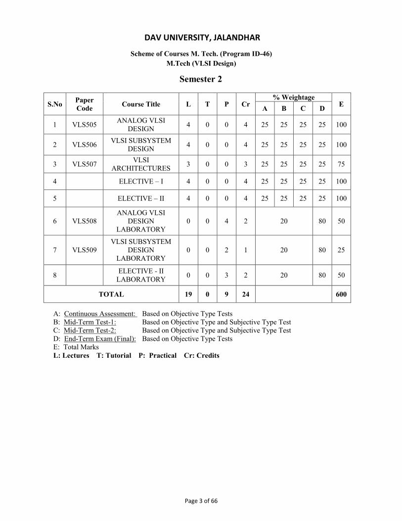
Semester 2
A: Continuous Assessment: Based on Objective Type Tests B: Mid-Term Test-1: Based on Objective Type and Subjective Type Test C: Mid-Term Test-2: Based on Objective Type and Subjective Type Test D: End-Term Exam (Final): Based on Objective Type Tests E: Total Marks L: Lectures T: Tutorial P: Practical Cr: Credits
S.No Paper Code Course Title L T P Cr
% Weightage E A B C D
1 VLS505 ANALOG VLSI DESIGN 4 0 0 4 25 25 25 25 100
2 VLS506 VLSI SUBSYSTEM DESIGN 4 0 0 4 25 25 25 25 100
3 VLS507 VLSI ARCHITECTURES 3 0 0 3 25 25 25 25 75
4 ELECTIVE – I 4 0 0 4 25 25 25 25 100
5 ELECTIVE – II 4 0 0 4 25 25 25 25 100
6 VLS508 ANALOG VLSI
DESIGN LABORATORY
0 0 4 2 20 80 50
7 VLS509 VLSI SUBSYSTEM
DESIGN LABORATORY
0 0 2 1 20 80 25
8 ELECTIVE - II LABORATORY 0 0 3 2 20 80 50
TOTAL 19 0 9 24 600
Page 3 of 66
DAV UNIVERSITY, JALANDHAR
Scheme of Courses M. Tech. (Program ID-46) M.Tech (VLSI Design)
Semester 3
A: Continuous Assessment: Based on Objective Type Tests B: Mid-Term Test-1: Based on Objective Type and Subjective Type Test C: Mid-Term Test-2: Based on Objective Type and Subjective Type Test D: End-Term Exam (Final): Based on Objective Type Tests E: Total Marks L: Lectures T: Tutorial P: Practical Cr: Credits
S.No Paper Code Course Title L T P Cr
% Weightage E A B C D
1 VLS601 LOW POWER VLSI DESIGN 3 0 0 3 25 25 25 25 75
2 ELECTIVE – III 4 0 0 4 25 25 25 25 100
3 ELECTIVE – IV 3 0 0 3 25 25 25 25 75
4 VLS602 RESEARCH SEMINAR 0 0 8 4 20 80 100
5 VLS603 THESIS (SYNOPSIS) 0 0 8 4 60 40 100
TOTAL 10 0 16 18 450
Page 4 of 66
DAV UNIVERSITY, JALANDHAR
Scheme of Courses M. Tech. (Program ID-46) M.Tech (VLSI Design)
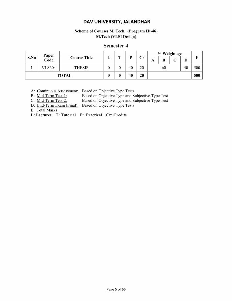
Semester 4
A: Continuous Assessment: Based on Objective Type Tests B: Mid-Term Test-1: Based on Objective Type and Subjective Type Test C: Mid-Term Test-2: Based on Objective Type and Subjective Type Test D: End-Term Exam (Final): Based on Objective Type Tests E: Total Marks L: Lectures T: Tutorial P: Practical Cr: Credits
S.No Paper Code Course Title L T P Cr
% Weightage E A B C D
1 VLS604 THESIS 0 0 40 20 60 40 500
TOTAL 0 0 40 20 500
Page 5 of 66
DAV UNIVERSITY, JALANDHAR
Scheme of Courses M. Tech (Program ID-46) M.Tech (VLSI Design)
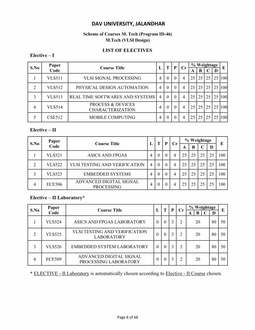
LIST OF ELECTIVES
Elective – I
S.No Paper Code Course Title L T P Cr % Weightage E A B C D
1 VLS511 VLSI SIGNAL PROCESSING 4 0 0 4 25 25 25 25 100
2 VLS512 PHYSICAL DESIGN AUTOMATION 4 0 0 4 25 25 25 25 100
3 VLS513 REAL TIME SOFTWARES AND SYSTEMS 4 0 0 4 25 25 25 25 100
4 VLS514 PROCESS & DEVICES CHARACTERIZATION 4 0 0 4 25 25 25 25 100
5 CSE512 MOBILE COMPUTING 4 0 0 4 25 25 25 25 100
Elective – II
S.No Paper Code Course Title L T P Cr
% Weightage E
A B C D
1 VLS521 ASICS AND FPGAS 4 0 0 4 25 25 25 25 100
2 VLS522 VLSI TESTING AND VERIFICATION 4 0 0 4 25 25 25 25 100
3 VLS523 EMBEDDED SYSTEMS 4 0 0 4 25 25 25 25 100
4 ECE506 ADVANCED DIGITAL SIGNAL PROCESSING 4 0 0 4 25 25 25 25 100
Elective – II Laboratory*
S.No Paper Code Course Title L T P Cr % Weightage E A B C D
1 VLS524 ASICS AND FPGAS LABORATORY 0 0 3 2 20 80 50
2 VLS525 VLSI TESTING AND VERIFICATION LABORATORY 0 0 3 2 20 80 50
3 VLS526 EMBEDDED SYSTEM LABORATORY 0 0 3 2 20 80 50
4 ECE509 ADVANCED DIGITAL SIGNAL PROCESSING LABORATORY 0 0 3 2 20 80 50
* ELECTIVE - II Laboratory is automatically chosen according to Elective - II Course chosen.
Page 6 of 66
DAV UNIVERSITY, JALANDHAR
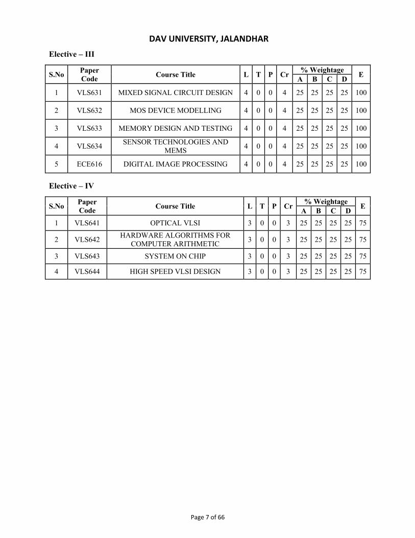
Elective – III
S.No Paper Code Course Title L T P Cr % Weightage E A B C D
1 VLS631 MIXED SIGNAL CIRCUIT DESIGN 4 0 0 4 25 25 25 25 100
2 VLS632 MOS DEVICE MODELLING 4 0 0 4 25 25 25 25 100
3 VLS633 MEMORY DESIGN AND TESTING 4 0 0 4 25 25 25 25 100
4 VLS634 SENSOR TECHNOLOGIES AND MEMS 4 0 0 4 25 25 25 25 100
5 ECE616 DIGITAL IMAGE PROCESSING 4 0 0 4 25 25 25 25 100
Elective – IV
S.No Paper Code Course Title L T P Cr % Weightage E A B C D
1 VLS641 OPTICAL VLSI 3 0 0 3 25 25 25 25 75
2 VLS642 HARDWARE ALGORITHMS FOR COMPUTER ARITHMETIC 3 0 0 3 25 25 25 25 75
3 VLS643 SYSTEM ON CHIP 3 0 0 3 25 25 25 25 75
4 VLS644 HIGH SPEED VLSI DESIGN 3 0 0 3 25 25 25 25 75
Page 7 of 66
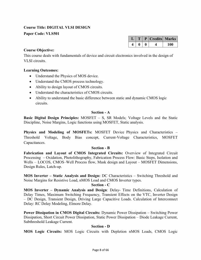
Course Title: DIGITAL VLSI DESIGN Paper Code: VLS501
L T P Credits Marks 4 0 0 4 100
Course Objective: This course deals with fundamentals of device and circuit electronics involved in the design of VLSI circuits. Learning Outcomes:
Understand the Physics of MOS device. Understand the CMOS process technology. Ability to design layout of CMOS circuits. Understand the characteristics of CMOS circuits. Ability to understand the basic difference between static and dynamic CMOS logic
circuits.
Section - A Basic Digital Design Principles: MOSFET – S, SR Models; Voltage Levels and the Static Discipline, Noise Margins, Logic functions using MOSFET, Static analysis. Physics and Modeling of MOSFETs: MOSFET Device Physics and Characteristics – Threshold Voltage, Body Bias concept, Current-Voltage Characteristics, MOSFET Capacitances.
Section - B Fabrication and Layout of CMOS Integrated Circuits: Overview of Integrated Circuit Processing – Oxidation, Photolithography, Fabrication Process Flow: Basic Steps, Isolation and Wells – LOCOS, CMOS–Well Process flow, Mask design and Layout – MOSFET Dimensions, Design Rules, Latch-up. MOS Inverter – Static Analysis and Design: DC Characteristics – Switching Threshold and Noise Margins for Resistive Load, nMOS Load and CMOS Inverter types.
Section - C MOS Inverter – Dynamic Analysis and Design: Delay- Time Definitions, Calculation of Delay Times, Maximum Switching Frequency, Transient Effects on the VTC, Inverter Design – DC Design, Transient Design, Driving Large Capacitive Loads. Calculation of Interconnect Delay: RC Delay Modeling, Elmore Delay. Power Dissipation in CMOS Digital Circuits: Dynamic Power Dissipation – Switching Power Dissipation, Short Circuit Power Dissipation, Static Power Dissipation – Diode Leakage Current, Subthreshold Leakage Current.
Section - D MOS Logic Circuits: MOS Logic Circuits with Depletion nMOS Loads, CMOS Logic
Page 8 of 66
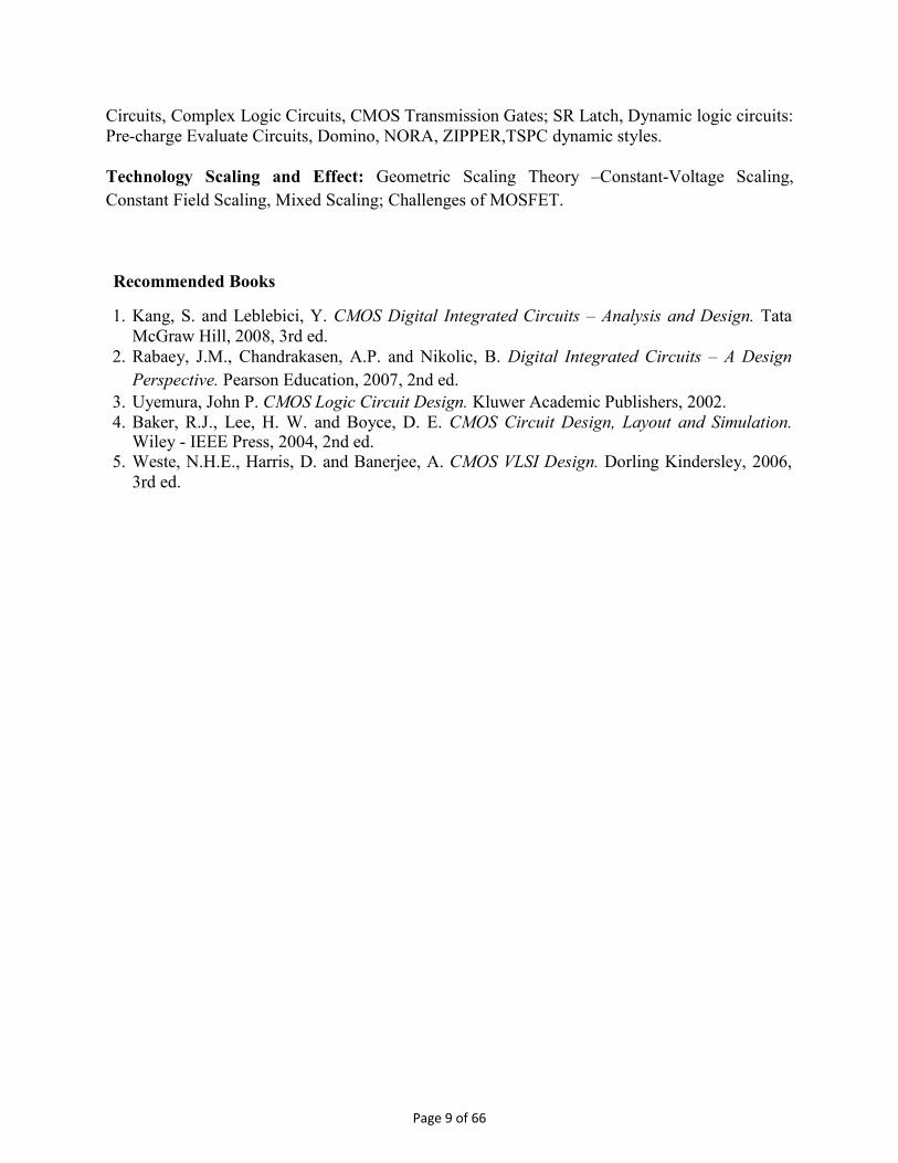
Circuits, Complex Logic Circuits, CMOS Transmission Gates; SR Latch, Dynamic logic circuits: Pre-charge Evaluate Circuits, Domino, NORA, ZIPPER,TSPC dynamic styles. Technology Scaling and Effect: Geometric Scaling Theory –Constant-Voltage Scaling, Constant Field Scaling, Mixed Scaling; Challenges of MOSFET.
Recommended Books
1. Kang, S. and Leblebici, Y. CMOS Digital Integrated Circuits – Analysis and Design. Tata McGraw Hill, 2008, 3rd ed.
2. Rabaey, J.M., Chandrakasen, A.P. and Nikolic, B. Digital Integrated Circuits – A Design Perspective. Pearson Education, 2007, 2nd ed.
3. Uyemura, John P. CMOS Logic Circuit Design. Kluwer Academic Publishers, 2002. 4. Baker, R.J., Lee, H. W. and Boyce, D. E. CMOS Circuit Design, Layout and Simulation.
Wiley - IEEE Press, 2004, 2nd ed. 5. Weste, N.H.E., Harris, D. and Banerjee, A. CMOS VLSI Design. Dorling Kindersley, 2006,
3rd ed.
Page 9 of 66
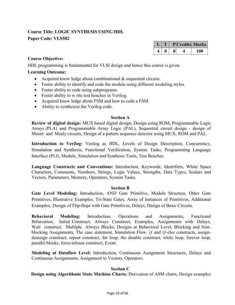
Course Title: LOGIC SYNTHESIS USING HDL Paper Code: VLS502
L T P Credits Marks 4 0 0 4 100
Course Objective: HDL programming is fundamental for VLSI design and hence this course is given. Learning Outcome:
Acquired know ledge about combinational & sequential circuits. Foster ability to identify and code the module using different modeling styles. Foster ability to code using subprograms. Foster ability to w rite test benches in Verilog. Acquired know ledge about FSM and how to code a FSM. Ability to synthesize the Verilog code.
Section A
Review of digital design: MUX based digital design, Design using ROM, Programmable Logic Arrays (PLA) and Programmable Array Logic (PAL), Sequential circuit design - design of Moore and Mealy circuits, Design of a pattern sequence detector using MUX, ROM and PAL.
Introduction to Verilog: Verilog as HDL, Levels of Design Description, Concurrency, Simulation and Synthesis, Functional Verification, System Tasks, Programming Language Interface (PLI), Module, Simulation and Synthesis Tools, Test Benches.
Language Constructs and Conventions: Introduction, Keywords, Identifiers, White Space Characters, Comments, Numbers, Strings, Logic Values, Strengths, Data Types, Scalars and Vectors, Parameters, Memory, Operators, System Tasks.
Section B Gate Level Modeling: Introduction, AND Gate Primitive, Module Structure, Other Gate Primitives, Illustrative Examples, Tri-State Gates, Array of Instances of Primitives, Additional Examples, Design of Flip-flops with Gate Primitives, Delays, Design of Basic Circuits.
Behavioral Modeling: Introduction, Operations and Assignments, Functional Bifurcation, Initial Construct, Always Construct, Examples, Assignments with Delays, Wait construct, Multiple Always Blocks, Designs at Behavioral Level, Blocking and Non-blocking Assignments, The case statement, Simulation Flow. iƒ and iƒ-else constructs, assign-deassign construct, repeat construct, for loop, the disable construct, while loop, forever loop, parallel blocks, force-release construct, Event.
Modeling at Dataflow Level: Introduction, Continuous Assignment Structures, Delays and Continuous Assignments, Assignment to Vectors, Operators.
Section C
Design using Algorithmic State Machine Charts: Derivation of ASM charts, Design examples
Page 10 of 66
such as dice game, etc. using ASM charts, Implementation of ASM charts using microprogramming, and Verilog design of bus arbitrator.
Test Benches: Test benches, verifying responses, clocks and resets, printing response values, reading data files, reading standard types, error handling.
Section D
Simulation, Synthesis, Place and Route, and Back Annotation: Design flow, Simulation using Modelsim, Synthesis using Synplify, Place and Route, and Back Annotation using Xilinx.
Design of memories: Verilog realization of Read Only Memory (ROM), Verilog realization of Random Access Memory (RAM), and Verilog coding of controller for accessing external memory.
Introduction to Hardware Implementation
Recommended Books:
1. Palnitkar, S. Verilog HDL: A Guide to Digital Design and Synthesis. PHI/Pearson, 1996. 2. Bhaskar, J. Verilog HDL Synthesis. BS publications, 2001. 3. Donald, P Leach and A P Malvino. Digital Principles and Applications. Tata McGraw-Hill Edition 2006.
Page 11 of 66
L T P Credits Marks 4 0 0 4 100
Course Title: Microelectronics Paper Code: ECE503
Course Objective: The course considers helps the students to understand Microelectronics
Learning Outcomes: Students will learn the practical aspects of Microelectronics and their uses
Section A
1. A Review of microelectronics and introduction to MOS technology: Introduction to IC technology, metal oxide semiconductor and related VLSI technology , Basic MOS transistors, enhancement and depletion model transistors, N-MOS and CMOS fabrication process, thermal aspects of processing, and production of E beam masks.
2. Electrical properties of MOS circuit: Parameters of MOS transistors, drain to source
current, threshold voltage, transconductance output conductance and figure of merit, pass transistor, N-MOS inverter, pull-up to pull down ratio for an N-MOS inverter, alternative forms of pull up
Section B
3. CMOS and BiCMOS Circuits: C-MOS inverters, MOS transistor circuit model, comparative aspects of key parameters of CMOS and bipolar transistor BiCMOS inverters, latch up in CMOS circuits, BiCMOS latch up susceptibility
4. Design processes: MOS layers, stick diagram, design rules and layout, double metal single poly silicon C-MOS process.
Section C
5. Basic circuit concepts: Sheets resistance, area capacitance, delay unit, inverter delay, super buffers, and propagation delays.
6. Scaling of MOS circuits: Scaling factor, limitations, scaling of wires and inter connections
Section D
7. Subsystem design & layout: Architectural issues, switch logic, gate logic, clocked sequential circuits, and other system consideration.
8. Ultra-fast VLSI circuits and systems: Ultra-fast systems, GaAs crystal structure, GaAs
devices, fabrication, device modeling and performance estimation.
Books Recommended:
1. DA. and Eshrachian K. Basic VLSI design systems & circuits. PHI, 1988. 2. Geigar, BR, Allen PE & Strader ME. VLSI design techniques for analog & digital circuit.
McGraw Hill, 1990.
Page 12 of 66

3. Related IEEE/IEE publications
Page 13 of 66
Course Title: Research Methodology Course Code: MGT551
Course Objective: The course is designed to introduce the students to research methodology and application of research techniques and procedures. The primary goal of this course is to develop a sound understanding of research methods.
Learning Outcomes: The students will be able to apply the various research methods by using computerized data analysis softwares to solve the real life problems.
Unit – A
Introduction to Research: Meaning of Research, Objectives of Research, Types of Research, Research Approaches, Significance of Research, Research Process, Criteria of Good Research, Problems Encountered by Researchers in India.
2 hour
Defining the Research Problem: What is a Research Problem?, Selecting the Problem, Necessity of Defining the Problem, Technique Involved in Defining a Problem
1 hour
Research Design: Meaning of Research Design, Need for Research Design, Features of a Good Design, Important Concepts Relating to Research Design, Different Research Designs, Basic Principles of Experimental Designs, factors affecting RDs, Relation among RDs, Developing a Research Plan.
2 hour
Unit – B
Sampling design and Procedures: Sample or Census, The Sampling Design Process, A Classification of Sampling Techniques, Choosing Nonprobability Versus Probability Sampling, Uses of Non probability Versus Probability Sampling.
2 hours
Measurement and Scaling: Non-comparative Scaling Techniques, Continuous Rating Scale, Itemized Rating Scale, Non-comparative Itemized Rating Scale Decisions, Multi-item Scales, Scale Evaluation, Choosing a Scaling Technique.
3 hours
Methods of Data Collection: Collection of Primary Data, Observation Method, Interview Method, Collection of Data through Questionnaires, Collection of Data through Schedules, Some Other Methods of Data Collection, Collection of Secondary Data, Selection of Appropriate Method for Data Collection.
3 hours
L T P Credits Marks 4 0 0 4 100
Page 14 of 66
Questionnaire & form design: questionnaire & observation forms, questionnaire design process.
2 hours
Unit – C
Data preparation: editing, coding, transcribing 1 Hours
Data analysis: tests of significance based on t, f and z distribution and chi-square test; cross tabulation
3 hours
Multiple Regression: Overview of Multiple Regression, Statistics Associated with Multiple Regression, Conducting Multiple Regression, Stepwise Regression, Multicollinearity
3 hours
Discriminant Analysis: Discriminant Analysis Model, Statistics Associated with Discriminant Analysis, Conducting Discriminant Analysis
4 hours
Conjoint Analysis: Basic Concepts in Conjoint Analysis, Statistics Associated with Conjoint Analysis, Conducting Conjoint Analysis, Assumptions & Limitations of Conjoint Analysis, Hybrid Conjoint Analysis
4 hours
Unit – D
Multi Dimensional Scaling: Basic Concepts in Multidimensional Scaling (MDS), Statistics Associated with MDS, Conducting Multidimensional Scaling, Selecting an MDS Procedure, Deciding on the Number of Dimensions, Labeling the Dimensions & Interpreting the Configuration, Assessing Reliability and Validity, Assumptions & Limitations of MDS, Scaling Preference Data
3 hours
Correspondence Analysis: Relationship between MDS, FA, & DA 2 hours
Factor Analysis: Factor Analysis Model, Statistics Associated with Factor Analysis, Conducting Factor Analysis, Applications of Common Factor Analysis
3 hour
Cluster Analysis: Statistics Associated with Cluster Analysis, Conducting Cluster Analysis, Applications of Non-hierarchical Clustering, Clustering Variables.
5 hours
Research Report Writing: Contents of Report, Executive Summary, Bibliography format. Presentation of Report. 2 hour
Total 45 hours
Page 15 of 66
Reference Books:
1. Bajpai Naval, Business Research Methods, Pearson Publications. 2. Malhotra, Naresh K. Marketing Research: An Applied Orientation, Pearson/Prentice-
Hall, 2007, 5th Edition. 3. Proctor Tony, Essentials of Marketing Research, Prentice Hall, 4th Edition 4. Beri G. C., Marketing research, McGrawHill, 4th Edition 5. C.R Kothari, Research Methodology, New Age Publishers
Page 16 of 66
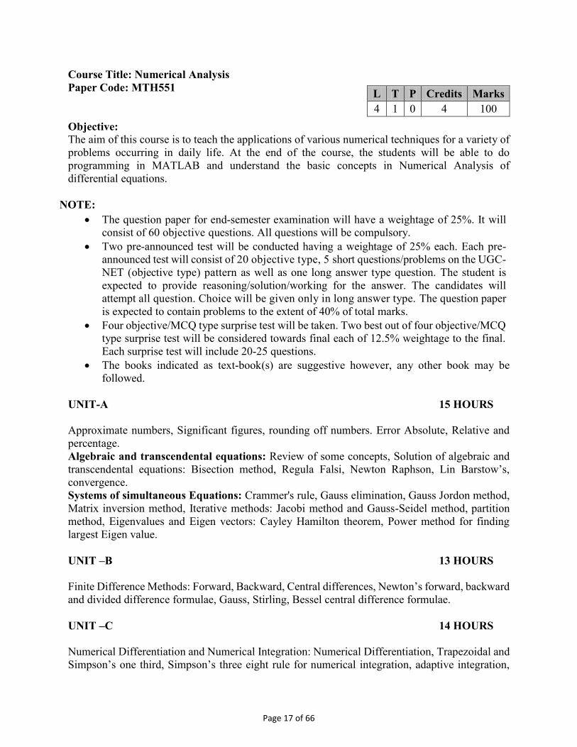
Course Title: Numerical Analysis Paper Code: MTH551 Objective: The aim of this course is to teach the applications of various numerical techniques for a variety of problems occurring in daily life. At the end of the course, the students will be able to do programming in MATLAB and understand the basic concepts in Numerical Analysis of differential equations.
NOTE: The question paper for end-semester examination will have a weightage of 25%. It will
consist of 60 objective questions. All questions will be compulsory. Two pre-announced test will be conducted having a weightage of 25% each. Each pre-
announced test will consist of 20 objective type, 5 short questions/problems on the UGC-NET (objective type) pattern as well as one long answer type question. The student is expected to provide reasoning/solution/working for the answer. The candidates will attempt all question. Choice will be given only in long answer type. The question paper is expected to contain problems to the extent of 40% of total marks.
Four objective/MCQ type surprise test will be taken. Two best out of four objective/MCQ type surprise test will be considered towards final each of 12.5% weightage to the final. Each surprise test will include 20-25 questions.
The books indicated as text-book(s) are suggestive however, any other book may be followed.
UNIT-A 15 HOURS Approximate numbers, Significant figures, rounding off numbers. Error Absolute, Relative and percentage. Algebraic and transcendental equations: Review of some concepts, Solution of algebraic and transcendental equations: Bisection method, Regula Falsi, Newton Raphson, Lin Barstow’s, convergence. Systems of simultaneous Equations: Crammer's rule, Gauss elimination, Gauss Jordon method, Matrix inversion method, Iterative methods: Jacobi method and Gauss-Seidel method, partition method, Eigenvalues and Eigen vectors: Cayley Hamilton theorem, Power method for finding largest Eigen value. UNIT –B 13 HOURS Finite Difference Methods: Forward, Backward, Central differences, Newton’s forward, backward and divided difference formulae, Gauss, Stirling, Bessel central difference formulae. UNIT –C 14 HOURS Numerical Differentiation and Numerical Integration: Numerical Differentiation, Trapezoidal and Simpson’s one third, Simpson’s three eight rule for numerical integration, adaptive integration,
L T P Credits Marks 4 1 0 4 100
Page 17 of 66
Taylor’s series method, Euler, modified Euler method, Runge-Kutta methods, Boole, weddle rule, Double integration. UNIT –D 14 HOURS Ordinary and Partial Differential Equations: Solution of second and higher order differential equations, boundary value problems, Solution of partial differential equations: Laplace, Heat, Wave equation. References:
1. Atkinson, K.E. An Introduction to Numerical Analysis. Wiley, 1989. 2. K. Eriksson, D. Estep, P. Hansbo and C. Johnson. Computational Differential Equations.
Cambridge, Cambridge Univ. Press, 1996. 3. G.H. Golub and J.M. Ortega. Scientific Computing and Differential Equations: An
Introduction to Numerical Methods. Academic Press, 1992. 4. S.D. Conte and Carl De Boor, Elementary Numerical Analysis, An Algorithmic Approach.
Tata McGraw Hill, New Delhi, 1981. 5. M.K. Jain, Numerical Analysis for Scientists and Engineers. S.B.W. Publishers, Delhi,
1971.
Page 18 of 66
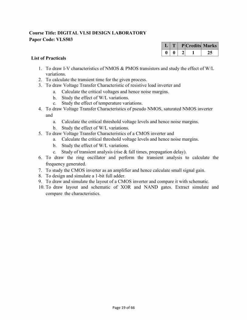
Course Title: DIGITAL VLSI DESIGN LABORATORY Paper Code: VLS503
L T P Credits Marks 0 0 2 1 25
List of Practicals
1. To draw I-V characteristics of NMOS & PMOS transistors and study the effect of W/L variations.
2. To calculate the transient time for the given process. 3. To draw Voltage Transfer Characteristic of resistive load inverter and
a. Calculate the critical voltages and hence noise margins. b. Study the effect of W/L variations. c. Study the effect of temperature variations.
4. To draw Voltage Transfer Characteristics of pseudo NMOS, saturated NMOS inverter and
a. Calculate the critical threshold voltage levels and hence noise margins. b. Study the effect of W/L variations.
5. To draw Voltage Transfer Characteristics of a CMOS inverter and a. Calculate the critical threshold voltage levels and hence noise margins. b. Study the effect of W/L variations. c. Study of transient analysis (rise & fall times, propagation delay).
6. To draw the ring oscillator and perform the transient analysis to calculate the frequency generated.
7. To study the CMOS inverter as an amplifier and hence calculate small signal gain. 8. To design and simulate a 1-bit full adder. 9. To draw and simulate the layout of a CMOS inverter and compare it with schematic. 10. To draw layout and schematic of XOR and NAND gates. Extract simulate and
compare the characteristics.
Page 19 of 66
Course Title: LOGIC SYTHESIS USING HDL LABORATORY Paper Code: VLS504
L T P Credits Marks 0 0 2 1 25
List of Practicals
1. Write a module declaration and a behavioral architecture of a two input multiplexer. 2. Write a module declaration and a structural architectural body for four-bit-wide
multiplexer, using instances of two-bit wide multiplexer. 3. Write a model for a counter with an output port of type natural, initially set to 15.
When the clock input changes to ‘1’, the counter decrements by one. After counting down to zero, the counter wraps back to 15-on the next clock edge.
4. Develop a model for priority encoder with a 16 element bit vector input port, an output port of type integer that encodes the index of leftmost ‘1’ value in the input and an output port of type bit that indicates whether any input elements are ‘1’.
5. Develop a model of a 4-bit full adder using generate statement. 6. Develop a behavioral for a D-latch with a clock-to-output propagation delay of 3ns
and a data- to-output propagation delay of 4ns.
7. Develop a behavioral model of a multiplexer with n select inputs, 2n data inputs and one data output.
8. Develop a structural model of a 4-bit adder using instances of a full adder component. Write a configuration declaration that binds each instance of the full adder component.
9. Develop a structural model of a n-bit-wide ripple carry adder. The least significant bits are added using a half-adder component, and the remaining bits are added using full-adder components.
10. Develop a behavioral model for a 3-bit parity generator and write its test bench. 11. Write a behavioral model of full-adder, and write test bench for it using files. 12. Write a model of a sequence generator detecting the sequence 1010, 1011 or 1001.
Page 20 of 66
Course Title: ANALOG IC DESIGN
Paper Code: VLS505
Course Objective: Analog circuits are essential in interfacing and in building amplifiers and low pass filters. This course introduces design methods for CMOS analog circuit design.
Learning Outcomes: Acquired knowledge about MOS transistor, low and high frequency models of MOSFET. Acquired knowledge about different active loads: MOS, Current Sources, Current Mirror
Circuits. Acquired knowledge to design and analyze different configurations of CMOS Amplifier Ability to learn and design CMOS differential amplifier, CMOS Op-Amp. Ability to learn the concept of feedback, and stability. Foster ability to learn and design CMOS comparators, Integrators etc.
Section – A Introduction to Analog VLSI: Analog integrated circuit design, Circuit design consideration for MOS challenges in analog circuit design, Recent trends in analog VLSI circuits. Analog MOSFET Modelling: MOSFET as a switch, MOSFET structuring, MOS Device Capacitances, MOS Device Layout, MOS Small-signal Model, MOS SPICE models, Long-Channel vs Short-Channel Devices.
Section – B CMOS Amplifier: Performances matrices of amplifier circuits, Common source amplifier, Common gate amplifier – Source Degeneration, Resistive, Diode-Connected and Current Source Load; Source Follower, Cascode amplifier, Frequency response of amplifiers and stability of amplifier. CMOS Differential Amplifier: Single-ended and Differential Operation, Qualitative and Quantitative Analysis, Common-Mode Response, Differential Pair with MOS loads.
Section – C Passive & Active Current Mirrors: Basic, Cascode Current Mirrors; Active Current Mirror – Large, Small, Common Mode. Frequency Response of Amplifiers: Miller-effect, Frequency response of - Common-source, Source follower, Common Gate, Cascode, Differential Amplifier. Noise – Types of noise, noise in different amplifiers. CMOS Feedback Amplifier: Feedback equation, Feedback Topology, Effect of Loading.
Section – D
L T P Credits Marks 4 0 0 4 100
Page 21 of 66
Stability and Frequency Compensation: Multi-pole Systems, Phase Margin, Frequency Compensation, Compensation Techniques. CMOS Operational amplifier: Block diagram of Op-amplifier, Ideal characteristics of Op-Amplifier, Design of single stage and two stage Op-Amplifier, Common-Mode feedback, slew-rate, Power Supply rejection.
Recommended Books:
1. Razavi, Behzad. Design of Analog CMOS Integrated Circuits. McGraw Hill, 2002. 2. Baker, R. Jacob and Harry W. Li, and David E. Boyce. CMOS: Circuit Design , Layout
and Simulation. Prentice Hall of India. 3. Johns, David A. and Ken Martin. Analog Integrated circuit Design. John Wiley & Son. 4. Allen, P.E. and Holberg, D.R. CMOS Analog Circuit Design. Oxford University Press.
2002, Indian 3rd ed.
Page 22 of 66
Course Title: VLSI SUBSYSTEM DESIGN
Paper Code: VLS506
Course Objective: The course aims to provide the fundamental knowledge about digital subsystem design techniques including data-processing, control, memory system designs.
Learning Outcomes: Ability to learn and understand the design methodologies and abstraction levels of CMOS
devices and circuits Acquire the knowledge of design of Digital Data Processing Circuits Ability to understand and design Mealy and Moore machines and their implementation Reinforce the understanding of standard Cell Libraries and their design Understanding of Memory Cell architectures and Memory System Design Ability to understand the Clocking Issues and solution
Section – A Introduction: Review of Transistor, Inverter Analysis, CMOS Process and Masking Sequence, Layer Properties and Parasitic Estimation. VLSI Design Flow, Design Methodologies, Abstraction Levels.
Section – B Design of Data Processing Elements: Adder Architectures, Multiplier Architectures, Counter Architectures, ALU Architectures, Design of Storage Elements: Latches, Flip-Flops, Registers, Register Files. Design of Control Part: Moore and Mealy Machines, PLA Based Implementation, Random Logic Implementation, Micro-programmed Implementation.
Section – C Structuring of Logic Design: PLA Design, PLA Architectures, Gates Array Cell Design, Concept of Standard Cell Based Design, Cell Library Design. Memory Design: SRAM cell, Various DRAM cells, RAM Architectures, Address Decoding, Read/Write Circuitry, Sense Amplifier and their Design, ROM Design.
Section – D Clocking Issues: Clocking Strategies, Clock Skew, Clock Distribution and Routing, Clock Buffering, Clock Domains, Gated Clock, Clock Tree.
Recommended Books
1. Weste, N.H.E. and Eshragian, K. Principles of CMOS VLSI Design – A Systems Perspective. Addison Wesley, 1994, 3rd ed.
2. Rabaey, J.M., Chandrakasan, A., and Nikolic, B. Digital Integrated Circuits – A Design Perspective. Pearson Education, 2008, 3rd ed.
3. Wolf, W., Modern VLSI Design. Prentice Hall, 2008, 3rd ed. 4. Mead, C. and Conway, L. Introduction to VLSI Systems. B.S. Publisher, 1980, 2nd ed. 5. Uyemura, J.P. Circuit design for CMOS VLSI. Springer, 2005, 2nd ed.
L T P Credits Marks 4 0 0 4 100
Page 23 of 66
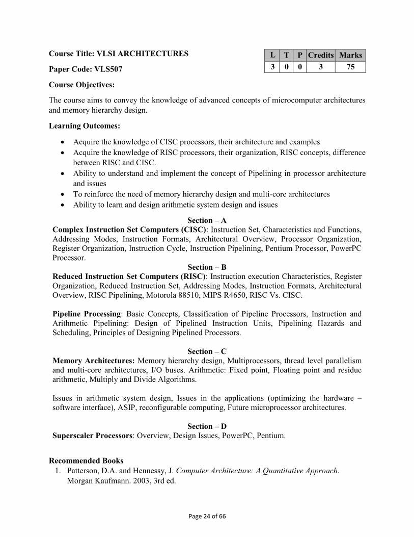
Course Title: VLSI ARCHITECTURES
Paper Code: VLS507
Course Objectives:
The course aims to convey the knowledge of advanced concepts of microcomputer architectures and memory hierarchy design.
Learning Outcomes:
Acquire the knowledge of CISC processors, their architecture and examples Acquire the knowledge of RISC processors, their organization, RISC concepts, difference
between RISC and CISC. Ability to understand and implement the concept of Pipelining in processor architecture
and issues To reinforce the need of memory hierarchy design and multi-core architectures Ability to learn and design arithmetic system design and issues
Section – A Complex Instruction Set Computers (CISC): Instruction Set, Characteristics and Functions, Addressing Modes, Instruction Formats, Architectural Overview, Processor Organization, Register Organization, Instruction Cycle, Instruction Pipelining, Pentium Processor, PowerPC Processor.
Section – B Reduced Instruction Set Computers (RISC): Instruction execution Characteristics, Register Organization, Reduced Instruction Set, Addressing Modes, Instruction Formats, Architectural Overview, RISC Pipelining, Motorola 88510, MIPS R4650, RISC Vs. CISC. Pipeline Processing: Basic Concepts, Classification of Pipeline Processors, Instruction and Arithmetic Pipelining: Design of Pipelined Instruction Units, Pipelining Hazards and Scheduling, Principles of Designing Pipelined Processors.
Section – C Memory Architectures: Memory hierarchy design, Multiprocessors, thread level parallelism and multi-core architectures, I/O buses. Arithmetic: Fixed point, Floating point and residue arithmetic, Multiply and Divide Algorithms. Issues in arithmetic system design, Issues in the applications (optimizing the hardware – software interface), ASIP, reconfigurable computing, Future microprocessor architectures.
Section – D Superscaler Processors: Overview, Design Issues, PowerPC, Pentium.
Recommended Books 1. Patterson, D.A. and Hennessy, J. Computer Architecture: A Quantitative Approach.
Morgan Kaufmann. 2003, 3rd ed.
L T P Credits Marks 3 0 0 3 75
Page 24 of 66
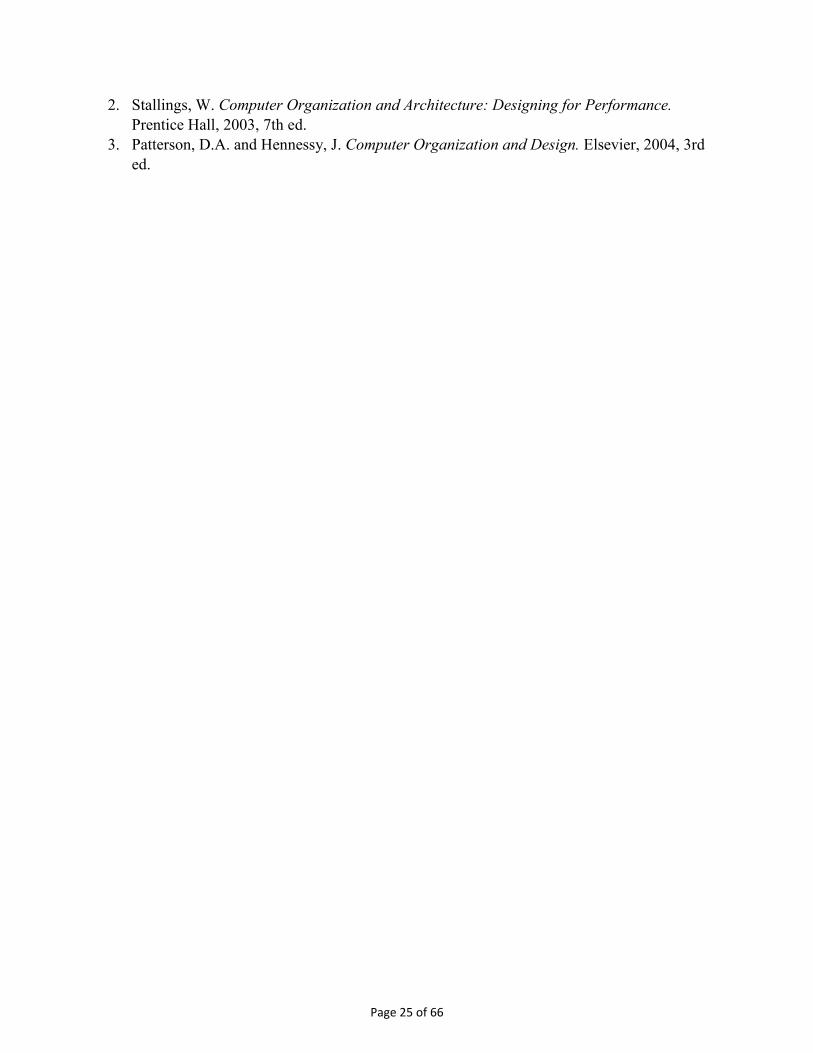
2. Stallings, W. Computer Organization and Architecture: Designing for Performance. Prentice Hall, 2003, 7th ed.
3. Patterson, D.A. and Hennessy, J. Computer Organization and Design. Elsevier, 2004, 3rd ed.
Page 25 of 66
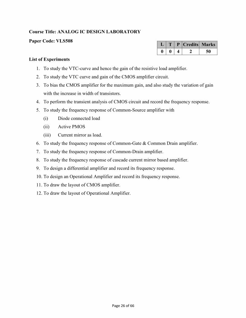
Course Title: ANALOG IC DESIGN LABORATORY
Paper Code: VLS508
List of Experiments
1. To study the VTC-curve and hence the gain of the resistive load amplifier.
2. To study the VTC curve and gain of the CMOS amplifier circuit.
3. To bias the CMOS amplifier for the maximum gain, and also study the variation of gain
with the increase in width of transistors.
4. To perform the transient analysis of CMOS circuit and record the frequency response.
5. To study the frequency response of Common-Source amplifier with
(i) Diode connected load
(ii) Active PMOS
(iii) Current mirror as load.
6. To study the frequency response of Common-Gate & Common Drain amplifier.
7. To study the frequency response of Common-Drain amplifier.
8. To study the frequency response of cascade current mirror based amplifier.
9. To design a differential amplifier and record its frequency response.
10. To design an Operational Amplifier and record its frequency response.
11. To draw the layout of CMOS amplifier.
12. To draw the layout of Operational Amplifier.
L T P Credits Marks 0 0 4 2 50
Page 26 of 66
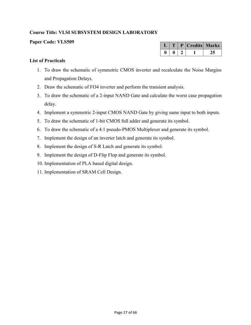
Course Title: VLSI SUBSYSTEM DESIGN LABORATORY
Paper Code: VLS509
List of Practicals
1. To draw the schematic of symmetric CMOS inverter and recalculate the Noise Margins
and Propagation Delays.
2. Draw the schematic of FO4 inverter and perform the transient analysis.
3. To draw the schematic of a 2-input NAND Gate and calculate the worst case propagation
delay.
4. Implement a symmetric 2-input CMOS NAND Gate by giving same input to both inputs.
5. To draw the schematic of 1-bit CMOS full adder and generate its symbol.
6. To draw the schematic of a 4:1 pseudo-PMOS Multiplexer and generate its symbol.
7. Implement the design of an inverter latch and generate its symbol.
8. Implement the design of S-R Latch and generate its symbol.
9. Implement the design of D-Flip Flop and generate its symbol.
10. Implementation of PLA based digital design.
11. Implementation of SRAM Cell Design.
L T P Credits Marks 0 0 2 1 25
Page 27 of 66
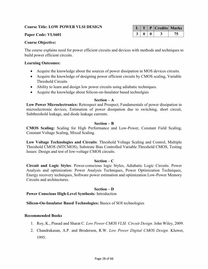
Course Title: LOW POWER VLSI DESIGN
Paper Code: VLS601
Course Objective:
The course explains need for power efficient circuits and devices with methods and techniques to build power efficient circuits.
Learning Outcomes:
Acquire the knowledge about the sources of power dissipation in MOS devices circuits. Acquire the knowledge of designing power efficient circuits by CMOS scaling, Variable
Threshold Circuits Ability to learn and design low power circuits using adiabatic techniques. Acquire the knowledge about Silicon-on-Insulator based technolgies
Section – A Low Power Microelectronics: Retrospect and Prospect, Fundamentals of power dissipation in microelectronic devices, Estimation of power dissipation due to switching, short circuit, Subthreshold leakage, and diode leakage currents.
Section – B CMOS Scaling: Scaling for High Performance and Low-Power, Constant Field Scaling, Constant Voltage Scaling, Mixed Scaling. Low Voltage Technologies and Circuits: Threshold Voltage Scaling and Control, Multiple Threshold CMOS (MTCMOS), Substrate Bias Controlled Variable Threshold CMOS, Testing Issues: Design and test of low-voltage CMOS circuits.
Section – C Circuit and Logic Styles: Power-conscious logic Styles, Adiabatic Logic Circuits. Power Analysis and optimization: Power Analysis Techniques, Power Optimization Techniques, Energy recovery techniques, Software power estimation and optimization Low-Power Memory Circuits and architectures.
Section – D Power Conscious High-Level Synthesis: Introduction Silicon-On-Insulator Based Technologies: Basics of SOI technologies
Recommended Books
1. Roy, K., Prasad and Sharat C. Low Power CMOS VLSI: Circuit Design. John Wiley, 2009.
2. Chandrakasan, A.P. and Broderson, R.W. Low Power Digital CMOS Design. Kluwer,
1995.
L T P Credits Marks 3 0 0 3 75
Page 28 of 66
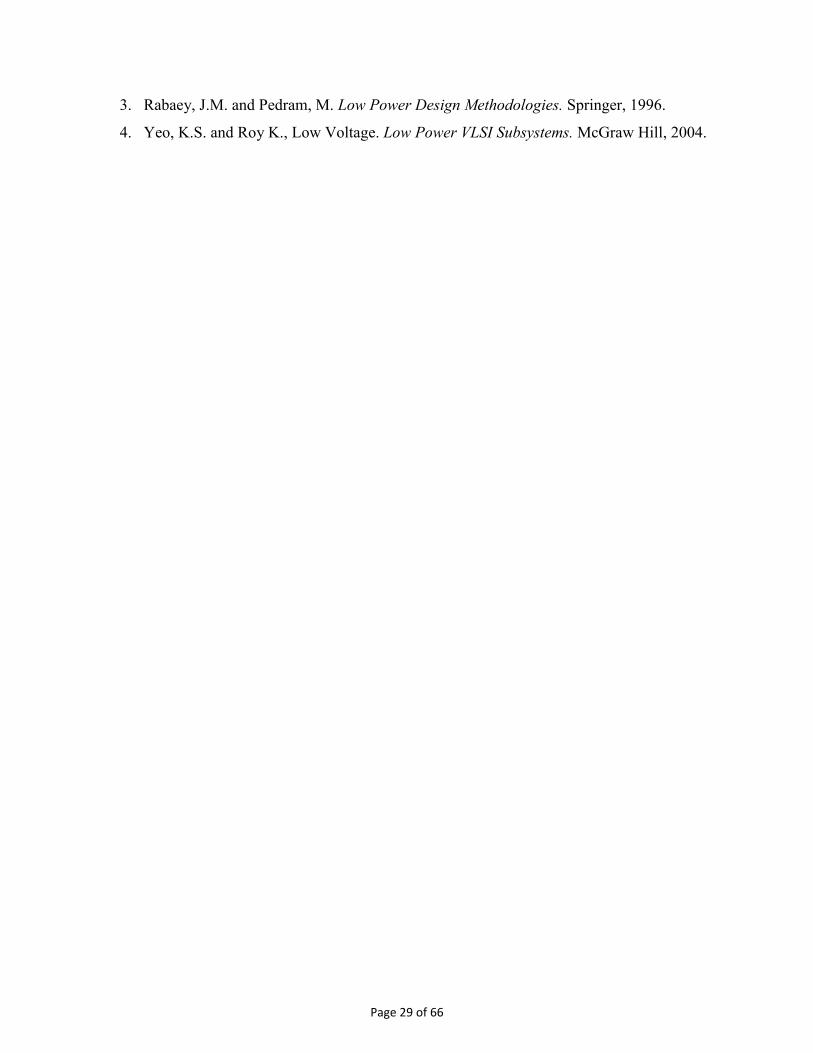
3. Rabaey, J.M. and Pedram, M. Low Power Design Methodologies. Springer, 1996.
4. Yeo, K.S. and Roy K., Low Voltage. Low Power VLSI Subsystems. McGraw Hill, 2004.
Page 29 of 66
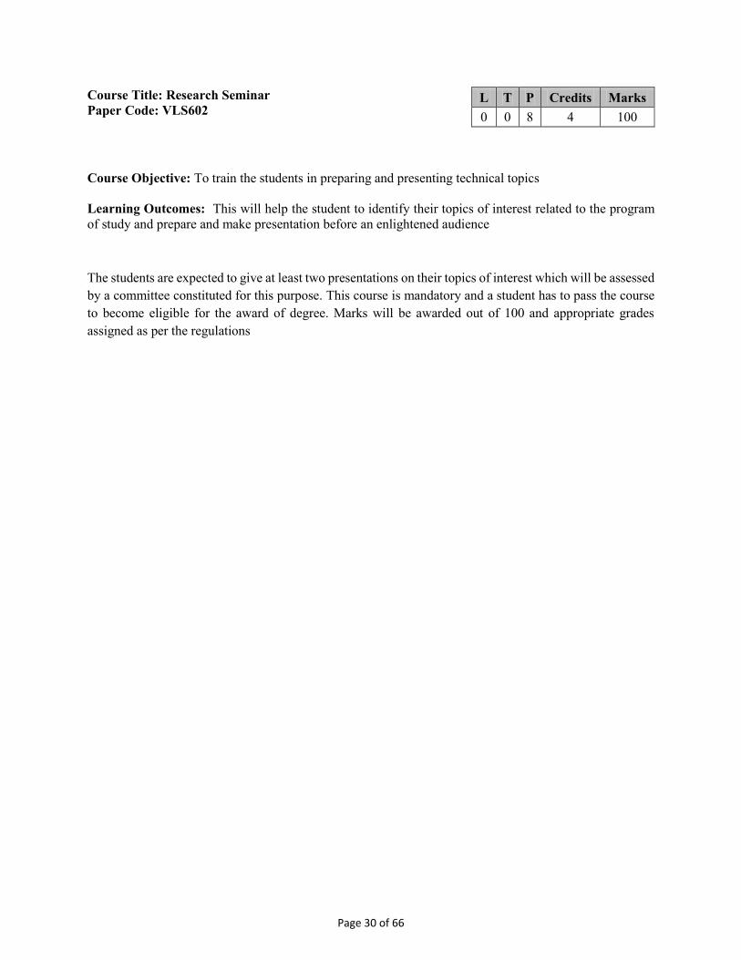
Course Title: Research Seminar Paper Code: VLS602
Course Objective: To train the students in preparing and presenting technical topics Learning Outcomes: This will help the student to identify their topics of interest related to the program of study and prepare and make presentation before an enlightened audience
The students are expected to give at least two presentations on their topics of interest which will be assessed by a committee constituted for this purpose. This course is mandatory and a student has to pass the course to become eligible for the award of degree. Marks will be awarded out of 100 and appropriate grades assigned as per the regulations
L T P Credits Marks 0 0 8 4 100
Page 30 of 66
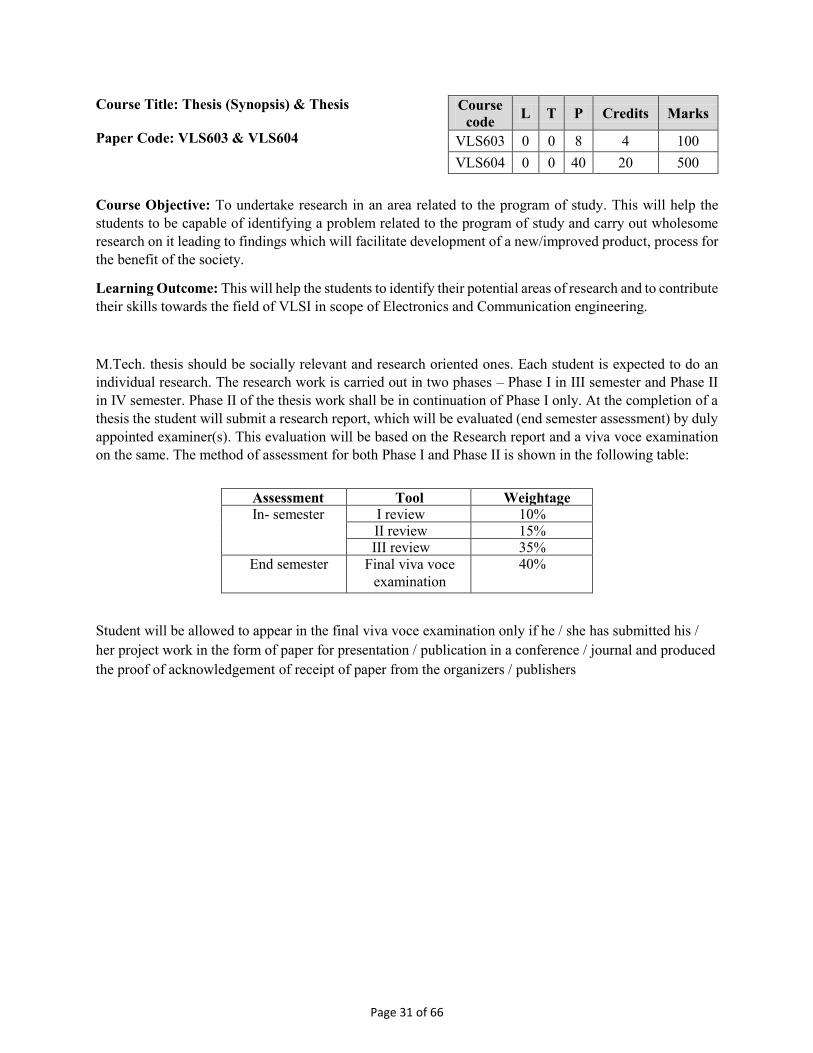
Course Title: Thesis (Synopsis) & Thesis Paper Code: VLS603 & VLS604 Course Objective: To undertake research in an area related to the program of study. This will help the students to be capable of identifying a problem related to the program of study and carry out wholesome research on it leading to findings which will facilitate development of a new/improved product, process for the benefit of the society.
Learning Outcome: This will help the students to identify their potential areas of research and to contribute their skills towards the field of VLSI in scope of Electronics and Communication engineering.
M.Tech. thesis should be socially relevant and research oriented ones. Each student is expected to do an individual research. The research work is carried out in two phases – Phase I in III semester and Phase II in IV semester. Phase II of the thesis work shall be in continuation of Phase I only. At the completion of a thesis the student will submit a research report, which will be evaluated (end semester assessment) by duly appointed examiner(s). This evaluation will be based on the Research report and a viva voce examination on the same. The method of assessment for both Phase I and Phase II is shown in the following table:
Assessment Tool Weightage In- semester I review 10%
II review 15% III review 35%
End semester Final viva voce examination
40%
Student will be allowed to appear in the final viva voce examination only if he / she has submitted his / her project work in the form of paper for presentation / publication in a conference / journal and produced the proof of acknowledgement of receipt of paper from the organizers / publishers
Course code L T P Credits Marks
VLS603 0 0 8 4 100 VLS604 0 0 40 20 500
Page 31 of 66
Course Title: OPTICAL VLSI
Paper Code: VLS641
Course Objective:
The course aims to strengthen the opto-electronic device knowledge blended with VLSI perception to study and understand the miniaturization and applications of the VLSI optical systems.
Section – A Introduction: Optical communication: An historical overview, Optical fiber versus copper wire, Integration of Optical communication systems, Optical communication link.
Section – B The CMOS Optical Receiver: Simple Resistor Optical Receiver, Trans-impedance amplifier, Comparison of trans-impedance amplifiers, Multiple-Stages feedback amplifiers, Noise aspects of the trans-impedance amplifier, Post amplifier.
Section – C Integrated CMOS Optical Receivers: DC-Coupled 0.8μm Digital CMOS 155 Mb/s Optical receiver; 240 Mb/s 18 THz Optical receiver with rail to rail output swing; 1 Gb/s 0.7μm standard CMOS optical receiver; Performance evaluation. Full Integration of a Standard CMOS Optical Transmitter: LED driver, Integrated CMOS optical fiber link, Integrated CMOS photodiodes, Integrated Photodiodes in sub-micron CMOS.
Section – D Electrical Interference in Mixed-Mode Integrated Circuits: Aspects of the electrical Interference Problem, Switching Noise Generation Reduction, On-chip Power supply Decoupling, Noise propagation limitation in integrated circuits, The Generalized use of differential structures in integrated circuits, Practical implementation.
Recommended Books
1. Ingels, M. and Steyaert, M. Integrated CMOS Circuits for Optical Communications. Springer, 2008.
2. Radovanoic, S., Anne-Johan, Annema and Bram, Nauta. High Speed Photodiodes in Standard CMOS Technology. Springer, 2006.
3. Muller, P. CMOS Multi-channel Single-Chip Receivers for Multi-Gigabit Optical Data Communications. Springer, 2007.
L T P Credits Marks 3 0 0 3 75
Page 32 of 66
Course Title: HARDWARE ALGORITHMS FOR COMPUTER ARITHMETIC
Paper Code: VLS642
Course Objectives:
Course aims to provide a thorough understanding of computer arithmetic algorithms, including different techniques enabling enhanced throughput and lower power. The students learn and understand algorithmic techniques to hardware implementation of various arithmetic operations.
Section – A Numbers and Arithmetic: Review of Number systems, their encoding and basic arithmetic operations, Class of Fixed-Radix Number Systems, Representing Signed Numbers, Negative-radix number Systems, Redundant Number Systems, Residue Number Systems.
Section – B Algorithms for Fast Addition: Basic Addition and Counting, Bit-serial and ripple-carry adders, Addition of a constant: counters, Manchester carry chains and adders, Simple carry-skip and Carry-select adders, Carry-Look-ahead Adders, Carry determination as prefix computation, Alternative parallel prefix networks, VLSI implementation aspects. High-Speed Multiplication: Basic Multiplication Schemes, Shift/add multiplication algorithms, Programmed multiplication, Basic hardware multipliers, Multiplication of signed numbers, Multiplication by constants, Preview of fast multipliers, High-Radix Multipliers, VLSI layout considerations.
Section – C Fast Division and Division Through Multiplication: Basic Division Schemes, Shift/subtract division algorithms, Programmed division, Restoring hardware dividers, Non-restoring and signed division, Division by constants, Combined multiply/divide units, Hardware implementation. Real Arithmetic: Representing the Real Numbers, Floating-point arithmetic, The ANSI/IEEE floating-point standard, Exceptions and other features, Floating-point arithmetic operations, Rounding schemes, Floating-point adders, Barrel-shifter design, Arithmetic Errors and Error Control.
Section – D Implementation Topics: High-Throughput Arithmetic, Low-Power Arithmetic, Fault-Tolerant Arithmetic, Emerging Trends, Impact of Hardware Technology.
Recommended Books
1. Parhami, B. Computer Arithmetic: Algorithms and Hardware Design. Oxford University Press, 2000.
2. Koren, I. Computer Arithmetic Algorithms. Uni Press, 2005, 2nd ed.
L T P Credits Marks 3 0 0 3 75
Page 33 of 66
3. Ercegovac, M. and Lang, T. Digital Arithmetic. Elsevier, 2005.
Page 34 of 66
Course Title: SYSTEM ON CHIP
Paper Code: VLS643
Course Objective: IP cores and application specific design is becoming the order of the day. Because of usefulness of this for both VLSI and embedded students this subject is provided.
Section – A Overview of SOC Design Process: Introduction, Top-down SoC design flow, Metrics of SoC design, Techniques to improve a specific design metric, ASIC Design flow and EDA tools.
Section – B SOC Architecture Design: Introduction, Front-end chip design, Back-end chip design, Integration platforms and SoC Design, Function Architecture Co-design, Designing Communication Networks, System Level Power Estimation and Modeling, Transaction Level Modeling, Design Space Exploration, Software design in SoCs.
Section – C SOC Design and Test Optimization: Design methodologies for SoC, Noise and signal integrity analysis, System Integration issues for SoC, SoC Test Scheduling and Test Integration, SoC Test Resource partition.
Section – D SOC Issues: Introduction, Hardware Software Co-design and issues.
Recommended Books
1. Wolf, W. Modern VLSI Design: System-on-chip Design. Prentice Hall, 2002, 3rd ed. 2. Nekoogar, F. and Nekoogar, F. From ASICs to SOCs: A Practical Approach. Prentice Hall,
2003. 3. Uyemura, J.P. Modern VLSI Design – SOC Design. Prentice Hall, 2001. 4. Lin, S.Y.L. Essential Issues in SOC Design: Designing Complex Systems-On-Chip.
Springer, 2004.
L T P Credits Marks 3 0 0 3 75
Page 35 of 66
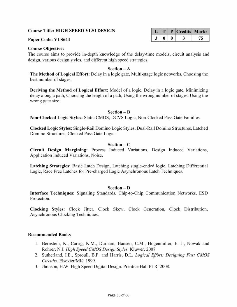
Course Title: HIGH SPEED VLSI DESIGN
Paper Code: VLS644
Course Objective: The course aims to provide in-depth knowledge of the delay-time models, circuit analysis and design, various design styles, and different high speed strategies.
Section – A The Method of Logical Effort: Delay in a logic gate, Multi-stage logic networks, Choosing the best number of stages. Deriving the Method of Logical Effort: Model of a logic, Delay in a logic gate, Minimizing delay along a path, Choosing the length of a path, Using the wrong number of stages, Using the wrong gate size.
Section – B Non-Clocked Logic Styles: Static CMOS, DCVS Logic, Non-Clocked Pass Gate Families. Clocked Logic Styles: Single-Rail Domino Logic Styles, Dual-Rail Domino Structures, Latched Domino Structures, Clocked Pass Gate Logic.
Section – C Circuit Design Margining: Process Induced Variations, Design Induced Variations, Application Induced Variations, Noise. Latching Strategies: Basic Latch Design, Latching single-ended logic, Latching Differential Logic, Race Free Latches for Pre-charged Logic Asynchronous Latch Techniques.
Section – D Interface Techniques: Signaling Standards, Chip-to-Chip Communication Networks, ESD Protection. Clocking Styles: Clock Jitter, Clock Skew, Clock Generation, Clock Distribution, Asynchronous Clocking Techniques.
Recommended Books
1. Bernstein, K., Carrig, K.M., Durham, Hansen, C.M., Hogenmiller, E. J., Nowak and Rohrer, N.J. High Speed CMOS Design Styles. Kluwer, 2007.
2. Sutherland, I.E., Sproull, B.F. and Harris, D.L. Logical Effort: Designing Fast CMOS Circuits. Elsevier/MK, 1999.
3. Jhonson, H.W. High Speed Digital Design. Prentice Hall PTR, 2008.
L T P Credits Marks 3 0 0 3 75
Page 36 of 66
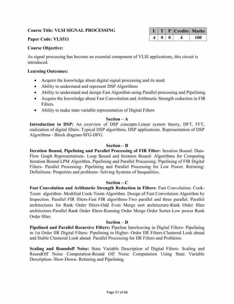
Course Title: VLSI SIGNAL PROCESSING
Paper Code: VLS511
Course Objective:
As signal processing has become an essential component of VLSI applications, this circuit is introduced.
Learning Outcomes:
Acquire the knowledge about digital signal processing and its need. Ability to understand and represent DSP Algorithms Ability to understand and design Fast Algorithm using Parallel processing and Pipelining Acquire the knowledge about Fast Convolution and Arithmetic Strength reduction in FIR
Filters. Ability to make state variable representation of Digital Filters
Section – A Introduction to DSP: An overview of DSP concepts-Linear system theory, DFT, FFT, realization of digital filters. Typical DSP algorithms, DSP applications. Representation of DSP Algorithms - Block diagram-SFG-DFG.
Section – B Iteration Bound, Pipelining and Parallel Processing of FIR Filter: Iteration Bound: Data-Flow Graph Representations- Loop Bound and Iteration Bound- Algorithms for Computing Iteration Bound-LPM Algorithm. Pipelining and Parallel Processing: Pipelining of FIR Digital Filters- Parallel Processing- Pipelining and Parallel Processing for Low Power. Retiming: Definitions- Properties and problems- Solving Systems of Inequalities.
Section – C Fast Convolution and Arithmetic Strength Reduction in Filters: Fast Convolution: Cook-Toom algorithm- Modified Cook-Toom Algorithm. Design of Fast Convolution Algorithm by Inspection. Parallel FIR filters-Fast FIR algorithms-Two parallel and three parallel. Parallel architectures for Rank Order filters-Odd Even Merge sort architecture-Rank Order filter architecture-Parallel Rank Order filters-Running Order Merge Order Sorter-Low power Rank Order filter.
Section – D Pipelined and Parallel Recursive Filters: Pipeline Interleaving in Digital Filters- Pipelining in 1st Order IIR Digital Filters- Pipelining in Higher- Order IIR Filters-Clustered Look ahead and Stable Clustered Look ahead- Parallel Processing for IIR Filters and Problems. Scaling and Roundoff Noise: State Variable Description of Digital Filters- Scaling and RoundOff Noise Computation-Round Off Noise Computation Using State Variable Description- Slow-Down- Retiming and Pipelining.
L T P Credits Marks 4 0 0 4 100
Page 37 of 66
Recommended Books
1. U. Meyer, Baese. Digital Signal Processing with FPGAs. Springer, 2004 2. K.K Parhi. VLSI Digital Signal processing. John-Wiley, 1999 3. Oppenheim, A.V. and Schafer, R.W. Discrete-Time Signal Processing. Prentice Hall,
2009, 2nd ed.
Page 38 of 66
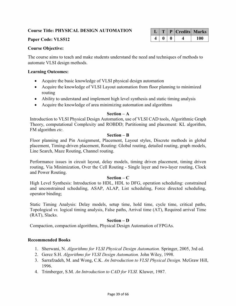
Course Title: PHYSICAL DESIGN AUTOMATION
Paper Code: VLS512
Course Objective:
The course aims to teach and make students understand the need and techniques of methods to automate VLSI design methods.
Learning Outcomes:
Acquire the basic knowledge of VLSI physical design automation Acquire the knowledge of VLSI Layout automation from floor planning to minimized
routing Ability to understand and implement high level synthesis and static timing analysis Acquire the knowledge of area minimizing automation and algorithms
Section – A Introduction to VLSI Physical Design Automation, use of VLSI CAD tools, Algorithmic Graph Theory, computational Complexity and ROBDD; Partitioning and placement: KL algorithm, FM algorithm etc.
Section – B Floor planning and Pin Assignment, Placement, Layout styles, Discrete methods in global placement, Timing-driven placement, Routing: Global routing, detailed routing, graph models, Line Search, Maze Routing, Channel routing. Performance issues in circuit layout, delay models, timing driven placement, timing driven routing, Via Minimization, Over the Cell Routing - Single layer and two-layer routing, Clock and Power Routing.
Section – C High Level Synthesis: Introduction to HDL, HDL to DFG, operation scheduling: constrained and unconstrained scheduling, ASAP, ALAP, List scheduling, Force directed scheduling, operator binding; Static Timing Analysis: Delay models, setup time, hold time, cycle time, critical paths, Topological vs. logical timing analysis, False paths, Arrival time (AT), Required arrival Time (RAT), Slacks.
Section – D Compaction, compaction algorithms, Physical Design Automation of FPGAs.
Recommended Books
1. Sherwani, N. Algorithms for VLSI Physical Design Automation. Springer, 2005, 3rd ed. 2. Gerez S.H. Algorithms for VLSI Design Automation. John Wiley, 1998. 3. Sarrafzadeh, M. and Wong, C.K. An Introduction to VLSI Physical Design. McGraw Hill,
1996. 4. Trimberger, S.M. An Introduction to CAD for VLSI. Kluwer, 1987.
L T P Credits Marks 4 0 0 4 100
Page 39 of 66
Course Title: REALTIME SOFTWARES AND SYSTEMS
Paper Code: VLS513
Course Objective:
The primary objectives of this course are to understand the concepts of Real Time systems and its applications.
Learning Outcomes:
The student will be able to gain an introduction to real-time operating systems (RTOS) an understanding of the basic building blocks of a typical RTOS and their design understanding the concept of a process and a task understand process synchronization and constraints between processes an understanding of the role of schedulers and schedulability as it relates to RTOS
Section – A Introduction to Real-Time System: Definition of a real-time system, Examples of real-time system, Characteristics of real-time system, Embedded Systems Components, Fundamentals of embedded system hardware and firmware design, Hard versus Soft Real-Time systems, Embedded processor selection, Embedded System Revolution, Reference Model of Real-Time Systems.
Section – B Real-Time Scheduling and Schedulability Analysis: Clock-driven scheduling, Priority-driven scheduling of periodic tasks, Scheduling a periodic and sporadic jobs in priority-driven systems, Function Queue Scheduling and Date Shard and Reentrancy.
Section – C Embedded Software: Examples of embedded system, Characteristic and Typical Hardware Components, Embedded Software Architectures, Round Robin, and Interrupts, Memory Architecture and Devices, Memory Interface. Fault Tolerance: Reliability, Failure and Faults, Failure modes, Fault prevention and Fault tolerance, N-version programming, Software dynamic redundancy, The recovery block approach to Software Fault Tolerance, A comparison between N-version programming and Recovery Blocks, Dynamic Redundancy and Exceptions, Measuring and Predicting the Reliability of software, Safety, Reliability and Dependability.
Section – D Application of Real-Time Systems: Real-Time Embedded Systems, Safety-Critical Systems, Real-time system requirements, Real-time system design, The Real-Time System production process, Performance estimation and optimization.
Recommended Books 1. Shaw, A.C. Real Time Systems and Software. John Wiley, 2001.
L T P Credits Marks 4 0 0 4 100
Page 40 of 66
2. Liu, J.W.S. Real Time Systems. Dorling Kindersley, 2008. 3. Khrisna, C.M. Real Time Systems. McGraw Hill, 1997. 4. Cheng, A.M.K. Real- Time Systems: Scheduling, Analysis and Verification. John Wiley,
2002 5. .
Page 41 of 66
Course Title: PROCESSES AND DEVICE CHARACTERIZATION
Paper Code: VLS514
Course Objectives: The course aims to provide the advanced physical, mechanical, electrical characterization of devices and techniques.
Learning Outcomes: Ability to understand and appreciate the underlying physics and principles involved in
silicon processing and device characterization Ability to relate theory on semiconductor processing and device physics to practical
technology development and device design considerations Ability to use of CAD tools as a design aid in process and device simulation
Section – A
Physical Characterization: Thin Film Thickness- Measurements-ellipsometry, surface profiling, spectrophotometry, FTIR. Critical Dimension Measurements: Optical microscope, Scanning Electron Microscope, Transmission Electron Microscope.
Section – B Material and Impurity Characterization: SIMS, XRD, EDAX. Electrical Characterization: Four-probe technique, Hall Effect, sheet resistance C-V measurements, DLTS, Carrier lifetime, impurity profiling, I-V measurements.
Section – C Process and SPICE model parameter Extraction: SPICE BSIM3 model parameter extraction and optimization, Intrinsic Most and extrinsic, parasitic element, EKV model, Gummel-Poon model, BSIM model. Test Structures for Process Characterization: Contact Resistors, Split Cross Bridge Resistors, Self-aligned n+ Bridges.
Section – D Test Structures for Device Characterization: Individual MOSFETs, 4x4 MOSFET Arrays, Capacitors. Test Structures for Faults and Reliability Analysis: Contact Chains, Serpentine/Comb Resistors.
Recommended Books
1. Runyan, W.R. and Shaffner, T.J. Semiconductor Measurements and Instrumentation. McGraw-Hill, 2006, 3rd ed.
2. Schroder, D.K. Semiconductor Material and Device Characterization. Wiley, 1998, 2nd ed.
L T P Credits Marks 4 0 0 4 100
Page 42 of 66
3. Kane, P.F. and Larrabee, G.B. Characterization of Semiconductor Materials. McGraw Hill (1970).
4. Ravi, K.V. Imperfections and Impurities in Semiconductor Silicon. John Wiley (1981).
Page 43 of 66
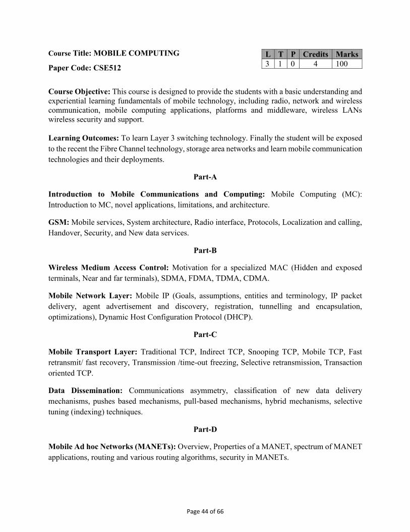
Course Title: MOBILE COMPUTING
Paper Code: CSE512
Course Objective: This course is designed to provide the students with a basic understanding and experiential learning fundamentals of mobile technology, including radio, network and wireless communication, mobile computing applications, platforms and middleware, wireless LANs wireless security and support. Learning Outcomes: To learn Layer 3 switching technology. Finally the student will be exposed to the recent the Fibre Channel technology, storage area networks and learn mobile communication technologies and their deployments.
Part-A
Introduction to Mobile Communications and Computing: Mobile Computing (MC): Introduction to MC, novel applications, limitations, and architecture.
GSM: Mobile services, System architecture, Radio interface, Protocols, Localization and calling, Handover, Security, and New data services.
Part-B
Wireless Medium Access Control: Motivation for a specialized MAC (Hidden and exposed terminals, Near and far terminals), SDMA, FDMA, TDMA, CDMA.
Mobile Network Layer: Mobile IP (Goals, assumptions, entities and terminology, IP packet delivery, agent advertisement and discovery, registration, tunnelling and encapsulation, optimizations), Dynamic Host Configuration Protocol (DHCP).
Part-C
Mobile Transport Layer: Traditional TCP, Indirect TCP, Snooping TCP, Mobile TCP, Fast retransmit/ fast recovery, Transmission /time-out freezing, Selective retransmission, Transaction oriented TCP.
Data Dissemination: Communications asymmetry, classification of new data delivery mechanisms, pushes based mechanisms, pull-based mechanisms, hybrid mechanisms, selective tuning (indexing) techniques.
Part-D
Mobile Ad hoc Networks (MANETs): Overview, Properties of a MANET, spectrum of MANET applications, routing and various routing algorithms, security in MANETs.
L T P Credits Marks 3 1 0 4 100
Page 44 of 66
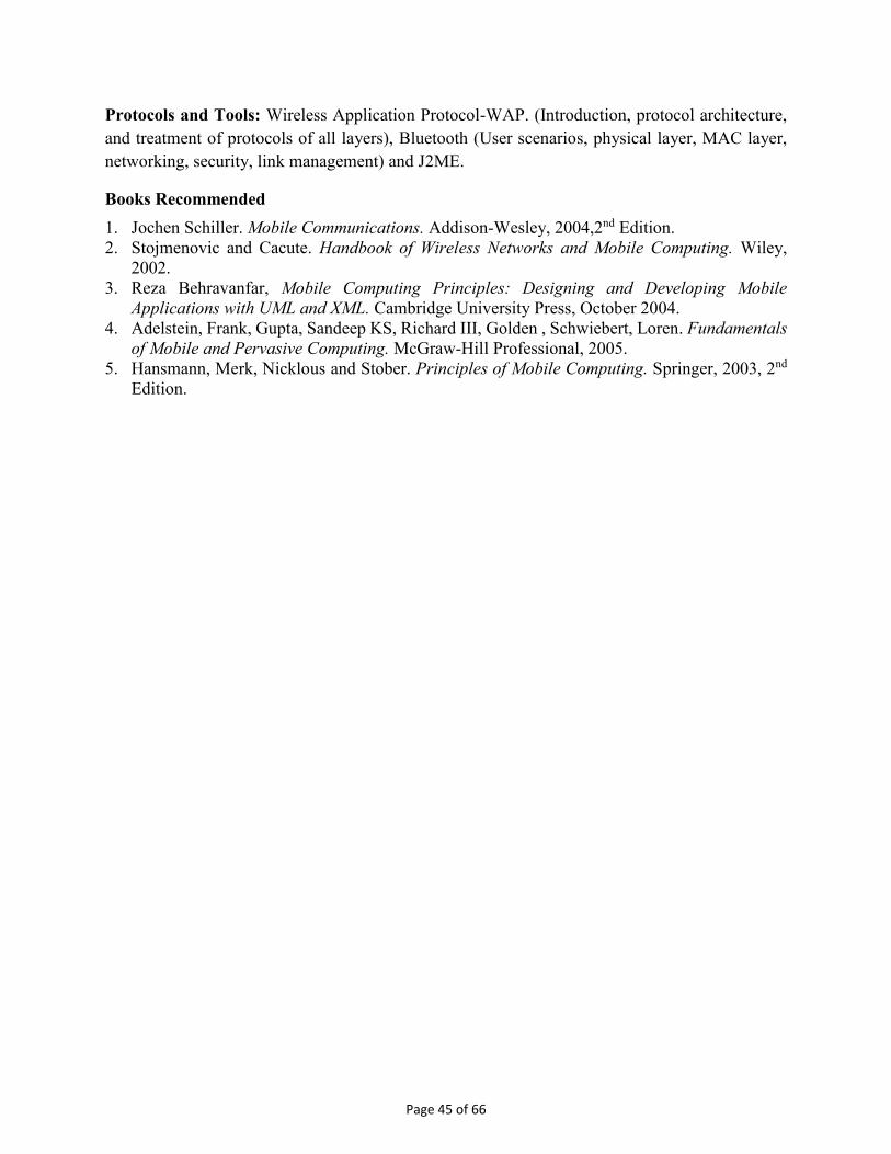
Protocols and Tools: Wireless Application Protocol-WAP. (Introduction, protocol architecture, and treatment of protocols of all layers), Bluetooth (User scenarios, physical layer, MAC layer, networking, security, link management) and J2ME.
Books Recommended 1. Jochen Schiller. Mobile Communications. Addison-Wesley, 2004,2nd Edition. 2. Stojmenovic and Cacute. Handbook of Wireless Networks and Mobile Computing. Wiley,
2002. 3. Reza Behravanfar, Mobile Computing Principles: Designing and Developing Mobile
Applications with UML and XML. Cambridge University Press, October 2004. 4. Adelstein, Frank, Gupta, Sandeep KS, Richard III, Golden , Schwiebert, Loren. Fundamentals
of Mobile and Pervasive Computing. McGraw-Hill Professional, 2005. 5. Hansmann, Merk, Nicklous and Stober. Principles of Mobile Computing. Springer, 2003, 2nd
Edition.
Page 45 of 66
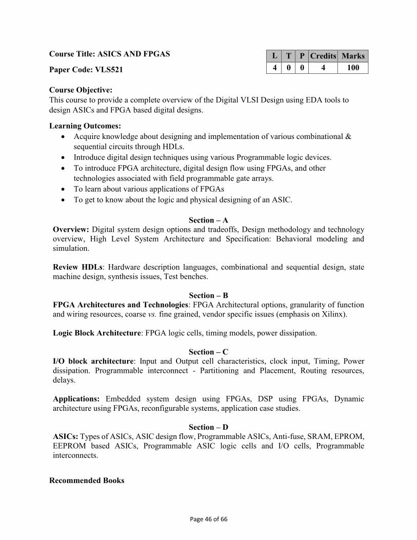
Course Title: ASICS AND FPGAS
Paper Code: VLS521 Course Objective: This course to provide a complete overview of the Digital VLSI Design using EDA tools to design ASICs and FPGA based digital designs.
Learning Outcomes: Acquire knowledge about designing and implementation of various combinational &
sequential circuits through HDLs. Introduce digital design techniques using various Programmable logic devices. To introduce FPGA architecture, digital design flow using FPGAs, and other
technologies associated with field programmable gate arrays. To learn about various applications of FPGAs To get to know about the logic and physical designing of an ASIC.
Section – A
Overview: Digital system design options and tradeoffs, Design methodology and technology overview, High Level System Architecture and Specification: Behavioral modeling and simulation. Review HDLs: Hardware description languages, combinational and sequential design, state machine design, synthesis issues, Test benches.
Section – B FPGA Architectures and Technologies: FPGA Architectural options, granularity of function and wiring resources, coarse vs. fine grained, vendor specific issues (emphasis on Xilinx). Logic Block Architecture: FPGA logic cells, timing models, power dissipation.
Section – C I/O block architecture: Input and Output cell characteristics, clock input, Timing, Power dissipation. Programmable interconnect - Partitioning and Placement, Routing resources, delays. Applications: Embedded system design using FPGAs, DSP using FPGAs, Dynamic architecture using FPGAs, reconfigurable systems, application case studies.
Section – D ASICs: Types of ASICs, ASIC design flow, Programmable ASICs, Anti-fuse, SRAM, EPROM, EEPROM based ASICs, Programmable ASIC logic cells and I/O cells, Programmable interconnects.
Recommended Books
L T P Credits Marks 4 0 0 4 100
Page 46 of 66
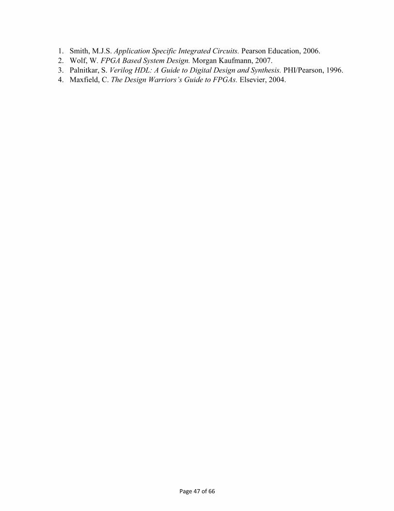
1. Smith, M.J.S. Application Specific Integrated Circuits. Pearson Education, 2006. 2. Wolf, W. FPGA Based System Design. Morgan Kaufmann, 2007. 3. Palnitkar, S. Verilog HDL: A Guide to Digital Design and Synthesis. PHI/Pearson, 1996. 4. Maxfield, C. The Design Warriors’s Guide to FPGAs. Elsevier, 2004.
Page 47 of 66
Course Title: VLSI TESTING AND VERIFICATION
Paper Code: VLS522
Course Objective: The main objective of this course is to study the concepts and techniques of VLSI design testing and verification to make a qualitative analysis and monitor critical design issues of design.
Learning Outcomes: 1. Fault modeling and simulation, Automatic Test Pattern Generation (ATPG), design for
testability (DFT), Scan and Boundary scan architectures, and built-in self-test (BIST) 2. Functional simulation, coverage metrics, event- and assertion-based verification, property
specification language, and formal methods including model checking and logical equivalence checking.
Section – A Faults: Physical Faults and their modeling; Stuck-at faults; Bridging Faults; Fault collapsing, Fault Simulation; Deductive, Parallel and Concurrent Fault Simulation; Critical Path Tracing. ATPG for Combinational Circuits: D-Algorithm, Boolean Difference, PODEM; Random, Exhaustive and Weighted Random Test Pattern Generation; Aliasing and its effect on Fault Coverage.
Section – B PLA Testing: Cross Point Fault Model and Test Generation. Memory Testing: Permanent, Intermittent and Pattern Sensitive Faults; Marching Tests; Delay Faults; ATPG for Sequential Circuits; Time Frame Expansion; Controllability and Observability Scan Design, ILBO, Boundary Scan for Board level Testing; BIST and Totally Self Checking Circuits; System Level diagnosis.
Section – C Introduction: Concept of Redundancy, Spatial Redundancy, Time Redundancy, Error Correction Codes; Reconfiguration Techniques; Yield Modeling Reliability and effective area utilization. Scope of testing and verification in VLSI design process, Issues in test and verification of complex chips, embedded cores and SoCs.
Section – D Verification: Design verification techniques based on simulation, analytical and formal approaches, Functional verification, Timing verification, Formal verification, Basics of equivalence checking and model checking, Hardware emulation.
Recommended Books
L T P Credits Marks 4 0 0 4 100
Page 48 of 66
1. Abramovici, M., Breuer, M. A. and Friedman, A.D. Digital Systems Testing and Testable Design, Jaico Publishing House, 2001.
2. Rashinkar, P., Paterson and Singh, L. System-on-a-Chip Verification-Methodology and Techniques, Kluwer Academic, 2001.
3. Bushnell, M. and Agrawal, V.D. Essentials of Electronic Testing for Digital, Memory and Mixed-Signal VLSI Circuits, Kluwer Academic, 2000.
4. Kropf, T., Introduction to Formal Hardware Verification, Springer Verlag, 1999.
Page 49 of 66
Course Title: EMBEDDED SYSTEMS
Paper Code: VLS523 Course Objective:
Course introduces system hardware and firmware design for embedded applications. It also teaches all aspects of design and development of an embedded system.
Learning Outcome: Acquire the knowledge of the basic ARM Microcontroller, and based embedded designs. Acquire the knowledge about embedded system design, firmware including programming
languages. Ability to learn and understand the RTOS concepts, including RTOS timers, interrupts,
system clock. Ability to learn and design 32-Bit ARM programming and hardware implementation
Section – A Introduction To Embedded System And Arm Architect: Challenges of Embedded Systems – Embedded system design process. Embedded processors – ARM processor – Architecture, ARM and Thumb Instruction sets.
Section – B Embedded C Programming: C-looping structures – Register allocation – Function calls – Pointer aliasing – structure arrangement – bit fields – unaligned data and endianness – inline functions and inline assembly – portability issues. Optimizing Assembly Code: Profiling and cycle counting – instruction scheduling – Register allocation – conditional execution – looping constructs – bit manipulation – efficient switches– optimized primitives.
Section – C RTOS Principle: Operating systems and its internals - Multitasking and Real time Operating Systems – Task Swapping Methods – Scheduler Algorithms – Priority Inversion – Task , Thread and Process – Choosing Operating System – Commercial Operating Systems – Linux.
Section – D Embedded Software Development Process: Meeting real time constraints – Multi-state systems and function sequences. Embedded software development tools – Emulators and debuggers. Design methodologies – Case studies – Complete design of example embedded systems.
Recommended Books 1. Mckenzie, Scott. The 8051 Microcontroller. PHI, 1995, 5th ed.
L T P Credits Marks 4 0 0 4 100
Page 50 of 66
2. Simon, David E. An Embedded System Primer. Pearson Education, 2005, 4th ed. 3. Prasad, K.V.K.K. Embedded/Real-time Systems: Concepts, Design and Programming.
Dreamtech press. 4. Dreamtech Software team. Proramming for Embedded Systems. Willey – Dreamtech 5. Andrew N Sloss, D. Symes and C. Wright, ARM system developers guide. Morgan
Kauffman/ Elsevier, 2006.
Page 51 of 66
L T P Credits Marks 4 0 0 4 100
Course Title: Advanced Digital Signal Processing Paper Code: ECE506
Course Objective: To introduce the student to advanced digital signal processing techniques.
Learning Outcomes:
• To study the parametric methods for power spectrum estimation. • To study adaptive filtering techniques using LMS algorithm and to study the applications
of adaptive filtering. • To study multi-rate signal processing fundamentals. • To study the analysis of signals. • To introduce the student to wavelet transforms
Section A
1. Multi rate Digital Signal Processing: Introduction to Multi-rate Digital Signal Processing, Sample rate reduction, decimation by integer factors, sampling rate increase, interpolation by integer factor, Design of practical sampling rate converters, sampling rate conversion using poly-phase filter structure, poly-phase implementation of interpolators.
Section B
2. Adaptive Signal Processing: Adaptive Signal Processing, Adaptive filters, Adaptive filter as a Noise Canceller, Other configurations of the adaptive filter, Main components of the adaptive filter, Basic Wiener filter theory, The basic LMS adaptive algorithm, Practical limitations of the basic LMS algorithm, Recursive Least Square Algorithm, Limitations, Factorization Algorithm.
Section C
3. Signal Transforms: Introduction to two dimensional signal and systems, 2D, DFT Transforms, Properties and applications, Discrete Hilbert Transform and Discrete Cosine Transform, Properties and Applications, Short term Fourier Transform, Gabor Transform, Properties and Applications.
4. Wavelet Transform: Limitations of Fourier and short time Fourier transform, Wavelets, Wavelet Analysis, The Continuous Wavelet Transform, scaling, shifting, scale and frequency, The Discrete Wavelet Transform, One Stage filtering, Approximation and Details, Filter bank analysis, Multilevel Decomposition, Number of levels, Wavelet reconstruction, Reconstruction filter- Reconstructing Approximations and details- Multilevel Reconstruction, Wavelet packet synthesis- Typical Applications.
Section D
5. DSP Processors: General and special purpose DSP Processors, Computer Architecture for signal processing, Havard Architecture, Pipelining, Hardware Multiply and Accumulate, Special Instructions, Replication , On-chip Memory Cache , Extended Parallelism, SIMD,
Page 52 of 66
VLIW and static super-scalar Processing, Brief study of TMS320C4X and ADSP 2106 processors.
Recommended Books
1. John G.Proakis and Dimitris G.Manobakis. Digital Signal Processing, Principles, Algorithms and Applications. PHI, 2000, Third edition.
2. Monson H.Hayes. Statistical Digital Signal Processing and Modeling. Wiley, 2002. 3. Emmanuel C Ifeachor and Barrie W Jrevis. Digital Signal Processing. Pearson Education. 4. L.R Rabiner and B Gold. Theory and Applications of DSP. 5. A .B Williams and FT Taylor. Electronic filter Design Hand Book. McGraw Hill. 6. Valterli & Kovaceric. Wavelets and Sub band Coding. PHI. 7. Analog Devices & Texas Instruments Users Manuel of TMS320C4X and ADSP 2106x.
Page 53 of 66
Course Title: ASICs & FPGAs LABORATORY
Paper Code: VLS524
Laboratory Work
1. Simulation/Implementation of Various Combinational Kernels on Xilinx/FPGA Boards: MUX based Designs PLA based Designs Adders, Fast Adders Multiplier, Shift-Add Multipliers Different variants of ALU
2. Simulation/Implementation of Various Sequential Systems on Xilinx/FPGA Boards: Counters, Registers Shift Registers, Barrel Shifters Gray Code Counters Arbitrary Sequence Counters, Sequence Generators Sequence Detectors
3. Simulation/Implementation of Various Digital Sub-Systems Kernels on Xilinx/FPGA Boards:
Traffic Light Controller Vending Machines Dice Games etc.
L T P Credits Marks 0 0 3 2 50
Page 54 of 66
Course Title: VLSI TESTING & VERIFICATION LABORATORY
Paper Code: VLS525
Laboratory Work:
Logic Simulations using Modelsim/Xilinx.
Logic Level Diagnostics
Functional Verification
Timing Verification
Basics of equivalence checking and model checking.
Totally Self Checking Circuits
Automatic Test Pattern Generation (ATPG) & simulation.
Implementation of BIST for given module
System Level diagnostics using DFT tools.
L T P Credits Marks 0 0 3 2 50
Page 55 of 66
Course Title: EMBEDDED SYSTEMS LABORATORY
Paper Code: VLS526
List of Experiments:
1. Write an ARM Assembly language program to find 2’s compliment of a number.
2. Write an ARM Assembly language program to load 32-bit data into a register and shift the
content to (i) left by 1 bit (ii) right by 1 bit (iii) right by 4 bits (iv) left by 4 bits if Zero Flag
is set.
3. Write an ARM Assembly program to disassemble 32-bit data into two 16-bit data.
4. Write an ARM Assembly program to add two 32-bit data stored in two consecutive
locations and store the result to some other location.
5. Write a program in ARM Assembly language to copy 8 consecutive words from source to
destination in memory using load and store instructions in a loop.
6. Write an ARM assembly program to arrange a given series of numbers in ascending order.
7. Write an ARM assembly program to count the number of 1’s and 0’s in a given word.
8. Write an ARM assembly program to calculate the value of the function: ax2+by2.
9. Write an ARM assembly program to perform division using repeated subtraction.
10. Write an ARM assembly program to convert ASCII value to Hexadecimal value.
11. Write an ARM assembly program to find the factorial of a given number using lookup
table.
12. Write an ARM assembly program to find the number of occurrences of a letter in a given
string.
L T P Credits Marks 0 0 3 2 50
Page 56 of 66
L T P Credits Marks 0 0 3 2 50
Course Title: Signal Processing Laboratory Paper Code: ECE509
Course Objective: To introduce the student to advanced digital signal processing techniques with help of MATLAB
Learning Outcomes: This will help the students to
• Study of the parametric methods for power spectrum estimation. • Study of adaptive filtering techniques using LMS algorithm and to study the
applications of adaptive filtering. • Study of multi-rate signal processing fundamentals. • Study of the analysis of signals.
List of Experiments
1. Experiment to demonstrate the sample rate reduction, interpolation and decimation using
MATLAB.
2. Experiment to demonstrate the adaptive filtering using MATLAB
3. Experiment to demonstrate Hilbert transform using MATLAB
4. Experiment to demonstrate DCT using MATLAB
5. Experiment to demonstrate STFT using MATLAB
6. Experiment to demonstrate Gabor transform using MATLAB
7. Experiment to demonstrate DWT using MATLAB
8. Experiment to demonstrate IDWT using MATLAB
9. Experiment to compare the various transform using MATLAB
Page 57 of 66
Course Title: MIXED SIGNAL CIRCUIT DESIGN
Paper Code: VLS631
Course Objective: As many real life applications involve both analog and digital circuits, this course aims to introduce the problems in implementing both in a single silicon wafer.
Learning Outcome: At the end of the course the student will be knowing mixed signal designs like DAC, ADC, PLL etc.
Section – A Non-Linear Analog Circuits: Characterization of a comparator, basic CMOS comparator design, Analog multiplier design, PLL – simple PLL, charge-pump PLL, applications of PLL. Switched Capacitor circuits – basic principles, some practical circuits such as switched capacitor integrator, biquad circuit, switched capacitor filter, switched capacitor amplifier, non-filtering applications of switched capacitor circuit such as programmable gate arrays, DAC and ADC, MOS comparators, modulators, rectifiers, detectors, oscillators.
Section – B Sampling Circuits: Basic sampling circuits for Analog signal sampling, performance metrics of sampling circuits, different types of sampling switches. Sample-and-Hold Architectures: Open-loop & closed-loop architectures, open-loop architecture with miller capacitance, multiplexed-input architectures, recycling architecture, switched capacitor architecture, current- mode architecture.
Section – C Digital-To Analog Conversion: Input/output characteristics of an ideal D/A converter, performance metrics of D/A converter, D/A converter in terms of voltage, current, and charge division or multiplication, switching functions to generate an analog output corresponding to a digital input. D/A converter architectures: Resistor-Ladder architectures, current-steering architectures. Analog-To-Digital Conversion: Input/output characteristics and quantization error of an A/D converter, performance metrics of A/D converter.
Section – D A/D converter architectures: Flash architectures, two-step architectures, interpolate and folding architectures, pipelined architectures, Successive approximation architectures, interleaved architectures. Analog Cmos Filters: Low Pass filters, active RC integrators, MOSFET-C integrators, trans-conductance-c integrator, and discrete time integrators. Filtering topologies – bilinear transfer function and biquadratic transfer function.
L T P Credits Marks 4 0 0 4 100
Page 58 of 66
Recommended Books
1. Razavi, B. Design of Analog CMOS integrated circuits. McGraw Hill, 2001. 2. Razavi, B. Principles of data conversion system design. S.Chand and company ltd, 2000. 3. Baker, Jacob. CMOS Mixed-Signal circuit design. IEEE Press, 2002. 4. Gregorian, Temes. Analog MOS Integrated Circuit for signal processing. John Wiley &
Sons. 5. Baker, Li and Boyce. CMOS : Circuit Design, layout and Simulation. PHI, 2000.
Page 59 of 66
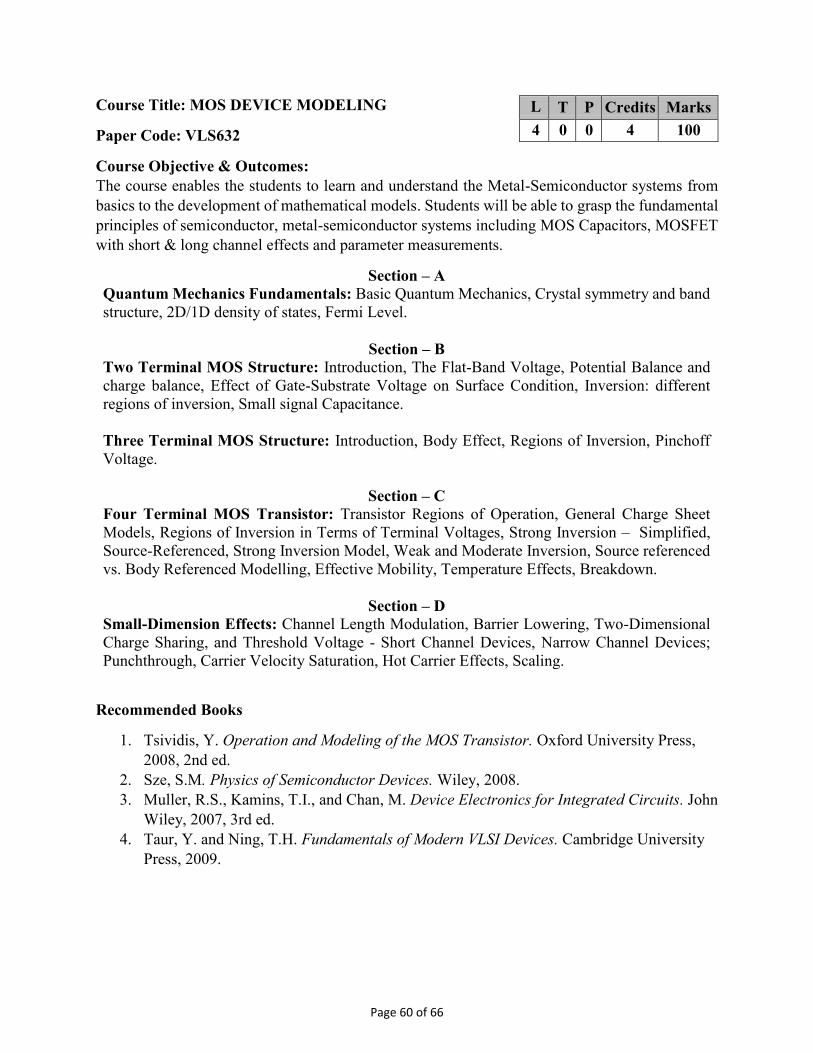
Course Title: MOS DEVICE MODELING
Paper Code: VLS632
Course Objective & Outcomes: The course enables the students to learn and understand the Metal-Semiconductor systems from basics to the development of mathematical models. Students will be able to grasp the fundamental principles of semiconductor, metal-semiconductor systems including MOS Capacitors, MOSFET with short & long channel effects and parameter measurements.
Section – A Quantum Mechanics Fundamentals: Basic Quantum Mechanics, Crystal symmetry and band structure, 2D/1D density of states, Fermi Level.
Section – B Two Terminal MOS Structure: Introduction, The Flat-Band Voltage, Potential Balance and charge balance, Effect of Gate-Substrate Voltage on Surface Condition, Inversion: different regions of inversion, Small signal Capacitance. Three Terminal MOS Structure: Introduction, Body Effect, Regions of Inversion, Pinchoff Voltage.
Section – C Four Terminal MOS Transistor: Transistor Regions of Operation, General Charge Sheet Models, Regions of Inversion in Terms of Terminal Voltages, Strong Inversion – Simplified, Source-Referenced, Strong Inversion Model, Weak and Moderate Inversion, Source referenced vs. Body Referenced Modelling, Effective Mobility, Temperature Effects, Breakdown.
Section – D Small-Dimension Effects: Channel Length Modulation, Barrier Lowering, Two-Dimensional Charge Sharing, and Threshold Voltage - Short Channel Devices, Narrow Channel Devices; Punchthrough, Carrier Velocity Saturation, Hot Carrier Effects, Scaling.
Recommended Books
1. Tsividis, Y. Operation and Modeling of the MOS Transistor. Oxford University Press, 2008, 2nd ed.
2. Sze, S.M. Physics of Semiconductor Devices. Wiley, 2008. 3. Muller, R.S., Kamins, T.I., and Chan, M. Device Electronics for Integrated Circuits. John
Wiley, 2007, 3rd ed. 4. Taur, Y. and Ning, T.H. Fundamentals of Modern VLSI Devices. Cambridge University
Press, 2009.
L T P Credits Marks 4 0 0 4 100
Page 60 of 66
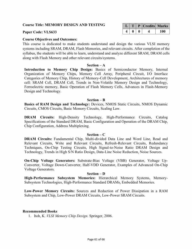
Course Title: MEMORY DESIGN AND TESTING
Paper Code: VLS633
Course Objectives and Outcomes: This course is dedicated to make students understand and design the various VLSI memory systems including SRAM, DRAM, Flash Memories, and relevant circuits. After completion of the syllabus, the students will be able to learn, understand and analyze different SRAM, DRAM cells along with Flash Memory and other relevant circuits/systems.
Section – A Introduction to Memory Chip Design: Basics of Semiconductor Memory, Internal Organization of Memory Chips, Memory Cell Array, Peripheral Circuit, I/O Interface Categories of Memory Chip, History of Memory-Cell Development, Architectures of memory cell: SRAM Cell, DRAM Cell, Trends in Non-Volatile Memory Design and Technology, Ferroelectric memory, Basic Operation of Flash Memory Cells, Advances in Flash-Memory Design and Technology.
Section – B Basics of RAM Design and Technology: Devices, NMOS Static Circuits, NMOS Dynamic Circuits, CMOS Circuits, Basic Memory Circuits, Scaling Law. DRAM Circuits: High-Density Technology, High-Performance Circuits, Catalog Specifications of the Standard DRAM, Basic Configuration and Operation of the DRAM Chip, Chip Configuration, Address Multiplexing.
Section – C DRAM Circuits: Fundamental Chip, Multi-divided Data Line and Word Line, Read and Relevant Circuits, Write and Relevant Circuits, Refresh-Relevant Circuits, Redundancy Techniques, On-Chip Testing Circuits, High Signal-to-Noise Ratio DRAM Design and Technology, Trends in High S/N Ratio Design, Data-Line Noise Reduction, Noise Sources. On-Chip Voltage Generators: Substrate-Bias Voltage (VBB) Generator, Voltage Up-Converter, Voltage Down-Converter, Half-VDD Generator, Examples of Advanced On-Chip Voltage Generators.
Section – D High-Performance Subsystem Memories: Hierarchical Memory Systems, Memory-Subsystem Technologies, High-Performance Standard DRAMs, Embedded Memories. Low-Power Memory Circuits: Sources and Reduction of Power Dissipation in a RAM Subsystem and Chip, Low-Power DRAM Circuits, Low-Power SRAM Circuits.
Recommended Books 1. Itoh, K. VLSI Memory Chip Design. Springer, 2006.
L T P Credits Marks 4 0 0 4 100
Page 61 of 66
2. Sharma, A. K., Semiconductor Memories: Technology, Testing and Reliability. Wiley- IEEE press, 2002.
3. Adams, R. D. High performance Memory Testing: Design Principles, Fault Modeling and Self-Test. Springer, 2002.
4. Sharma, A. K. Advanced Semiconductor Memories: Architecture, Design and Applications. John Wiley, 2002.
Page 62 of 66
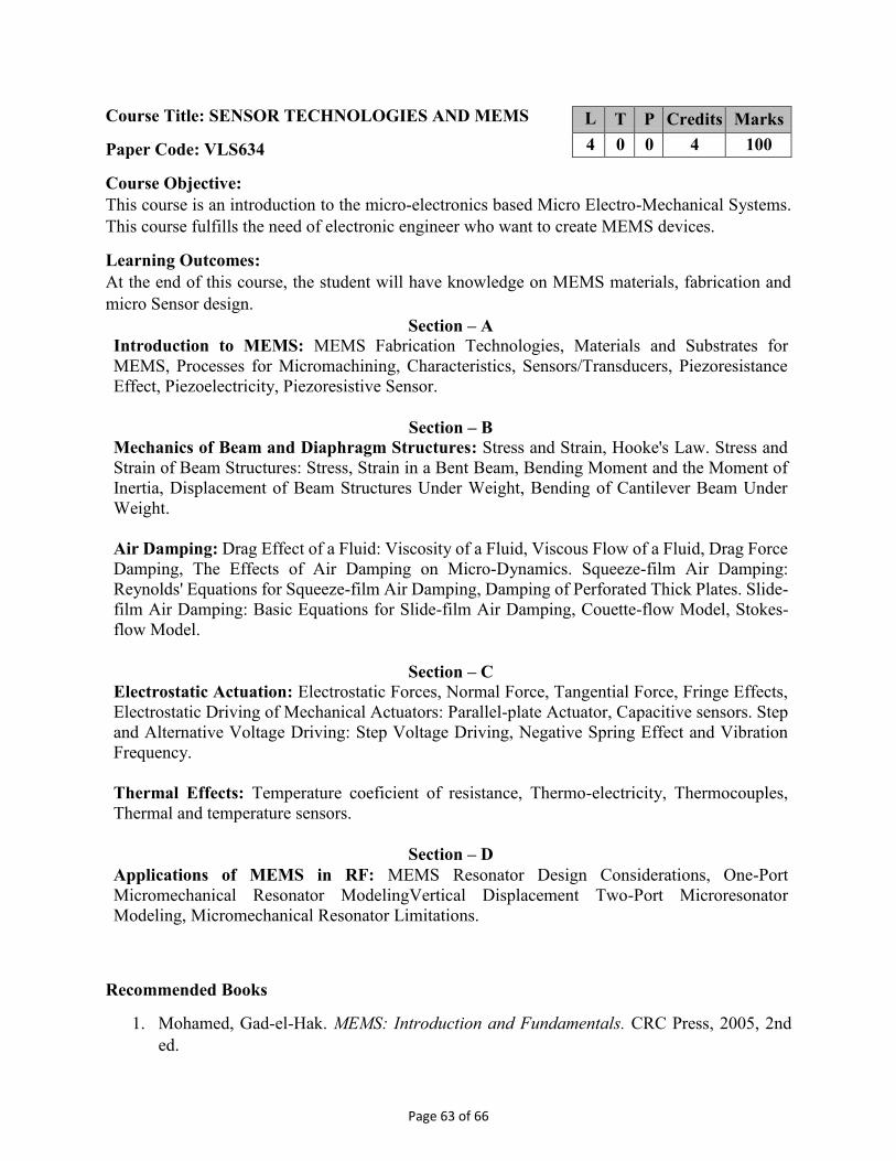
Course Title: SENSOR TECHNOLOGIES AND MEMS
Paper Code: VLS634
Course Objective: This course is an introduction to the micro-electronics based Micro Electro-Mechanical Systems. This course fulfills the need of electronic engineer who want to create MEMS devices.
Learning Outcomes: At the end of this course, the student will have knowledge on MEMS materials, fabrication and micro Sensor design.
Section – A Introduction to MEMS: MEMS Fabrication Technologies, Materials and Substrates for MEMS, Processes for Micromachining, Characteristics, Sensors/Transducers, Piezoresistance Effect, Piezoelectricity, Piezoresistive Sensor.
Section – B Mechanics of Beam and Diaphragm Structures: Stress and Strain, Hooke's Law. Stress and Strain of Beam Structures: Stress, Strain in a Bent Beam, Bending Moment and the Moment of Inertia, Displacement of Beam Structures Under Weight, Bending of Cantilever Beam Under Weight. Air Damping: Drag Effect of a Fluid: Viscosity of a Fluid, Viscous Flow of a Fluid, Drag Force Damping, The Effects of Air Damping on Micro-Dynamics. Squeeze-film Air Damping: Reynolds' Equations for Squeeze-film Air Damping, Damping of Perforated Thick Plates. Slide-film Air Damping: Basic Equations for Slide-film Air Damping, Couette-flow Model, Stokes-flow Model.
Section – C Electrostatic Actuation: Electrostatic Forces, Normal Force, Tangential Force, Fringe Effects, Electrostatic Driving of Mechanical Actuators: Parallel-plate Actuator, Capacitive sensors. Step and Alternative Voltage Driving: Step Voltage Driving, Negative Spring Effect and Vibration Frequency. Thermal Effects: Temperature coeficient of resistance, Thermo-electricity, Thermocouples, Thermal and temperature sensors.
Section – D Applications of MEMS in RF: MEMS Resonator Design Considerations, One-Port Micromechanical Resonator ModelingVertical Displacement Two-Port Microresonator Modeling, Micromechanical Resonator Limitations.
Recommended Books
1. Mohamed, Gad-el-Hak. MEMS: Introduction and Fundamentals. CRC Press, 2005, 2nd ed.
L T P Credits Marks 4 0 0 4 100
Page 63 of 66
2. Maluf, N. An Introduction to Micro-Electro-Mechanical Systems Engineering. Artech House, 2000.
3. Sze , S.M. Semiconductor Sensors. John Wiley & Sons Inc., Wiley Interscience Pub. 4. Usher, M.J. Sensors and Transducers. McMillian Hampshire.
Page 64 of 66
L T P Credits Marks 4 0 0 4 100
Course Title: Digital Image Processing Paper Code: ECE616 Course Objective: This will help students to understand fundamentals as well as advanced aspects of image processing Learning Outcome: After successful completion of this course, students will be able to perform various applications of image processing
Section A 1. Image Representation and Modeling: Fourier transform, z- transform, optical and modulation transfer functions, Matrix theory results, block matrices, Random signals, Discrete random fields, spectral density functions, results from estimation theory. 2. Image Perception: Light, luminance, brightness and contrast, MTF of Visual system, Visibility function, Monochrome vision methods, Image fidelity criteria, color matching and reproduction, color coordinate systems, color difference measures, color vision model, Temporal properties of vision.
Section B
3. Image Sampling & Quantization: Introduction, two dimensional sampling theory, Extensions of sampling theory, Practical limitations in sampling and reconstruction, Image Quantization, Optimum mean square or lloyd Max quantizer, A compandor design. 4. Image Transform: Two dimensional orthogonal and unitary transforms, properties of unitary transforms, Two dimensional DFT, Cosine transform, KL-transform.
Section C
5. Image Representation by Stochastic Models: Introduction, One dimensional causal models, One dimensional Spectral Factorization, AR Models, linear prediction in two dimension, Image decomposition, Fast KL transforms. 6. Image Enhancement: Point Operations, Spatial Operations, Transform Operations, Multispectral Image Enhancement, False Color and pseudocolor, color image enhancement
Section D
7. Image Filtering and Restoration: Introduction, Image observation models, Inverse and Wiener filtering, FIR Wiener filters, Fourier domain filters, filtering using image transforms, Smoothing splines and Interpolation, least square filters, Generalized inverse, SVD and Iterative methods, Recursive filtering for state variable system, causal models, Semi-causal models, Digital processing of speckle images, Maximum entropy restoration, Bayesian methods. Recommended Books: 1. Keenneth R Castleman. Digital Image Processing. Pearson Education Society. 2. Rafact Gonzalez and Richard E. Woods, Digital Image Processing. Pearson Edu. Society.
Page 65 of 66

3. Related IEEE/IEE Publications.
Page 66 of 66
Related Documents