Continuous-Time Analog Circuits for Statistical Signal Processing by Benjamin Vigoda Submitted to the Program in Media Arts and Sciences, School of Architecture and Planning in partial fulfillment of the requirements for the degree of Doctor of Philosophy at the MASSACHUSETTS INSTITUTE OF TECHNOLOGY September 2003 @ Massachusetts Institute of Technology 2003. All rights reserved. /1 Author.......... Program in Media Arts and Sciences, School of Architecture and Planning August 15, 2003 Certified by .................. i. . Neil Gershenfeld Associate Professor Thesis Supervisor Accepted by ... . . . .. . . . . . . . . . . . .(. . Andr w B. Lippman Chair, Department Committee on Graduate Students ROTCH MASSACHUSETTS INSTITUTE OF TECHNOLOGY SEP 2 9 2003 LBRARIES

Welcome message from author
This document is posted to help you gain knowledge. Please leave a comment to let me know what you think about it! Share it to your friends and learn new things together.
Transcript
Continuous-Time Analog Circuits for Statistical
Signal Processing
by
Benjamin Vigoda
Submitted to the Program in Media Arts and Sciences,School of Architecture and Planning
in partial fulfillment of the requirements for the degree of
Doctor of Philosophy
at the
MASSACHUSETTS INSTITUTE OF TECHNOLOGY
September 2003
@ Massachusetts Institute of Technology 2003. All rights reserved.
/1
Author..........Program in Media Arts and Sciences,School of Architecture and Planning
August 15, 2003
Certified by .................. i. .Neil Gershenfeld
Associate ProfessorThesis Supervisor
Accepted by ... . . . .. . . . . . . . . . . . .(. .Andr w B. Lippman
Chair, Department Committee on Graduate Students
ROTCHMASSACHUSETTS INSTITUTE
OF TECHNOLOGY
SEP 2 9 2003
LBRARIES

- --- C . . .-. .. .. '.. -. ..- 9 ''- .;. 's:' - .'':;;2-_'4'-- - ;
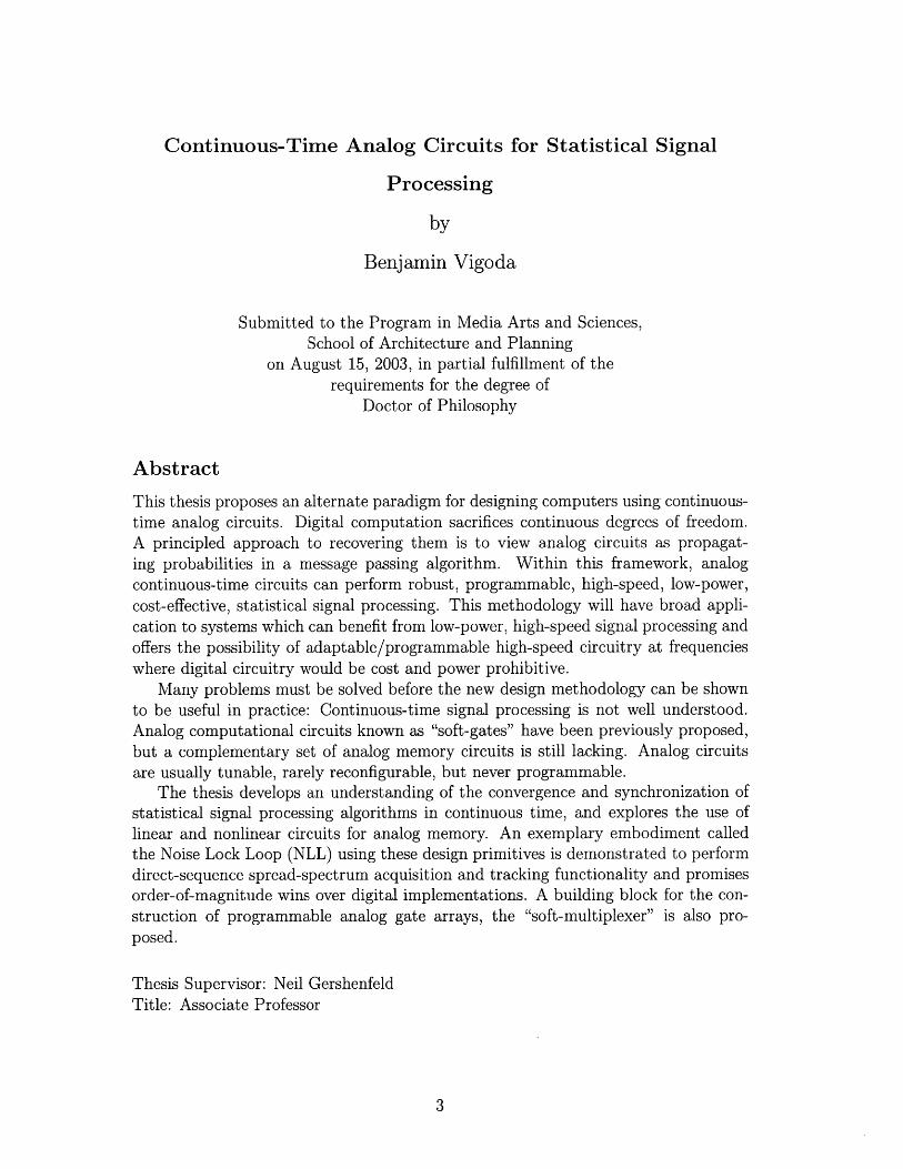
Continuous-Time Analog Circuits for Statistical Signal
Processing
by
Benjamin Vigoda
Submitted to the Program in Media Arts and Sciences,School of Architecture and Planning
on August 15, 2003, in partial fulfillment of therequirements for the degree of
Doctor of Philosophy
Abstract
This thesis proposes an alternate paradigm for designing computers using continuous-time analog circuits. Digital computation sacrifices continuous degrees of freedom.A principled approach to recovering them is to view analog circuits as propagat-ing probabilities in a message passing algorithm. Within this framework, analogcontinuous-time circuits can perform robust, programmable, high-speed, low-power,cost-effective, statistical signal processing. This methodology will have broad appli-cation to systems which can benefit from low-power, high-speed signal processing andoffers the possibility of adaptable/programmable high-speed circuitry at frequencieswhere digital circuitry would be cost and power prohibitive.
Many problems must be solved before the new design methodology can be shownto be useful in practice: Continuous-time signal processing is not well understood.Analog computational circuits known as "soft-gates" have been previously proposed,but a complementary set of analog memory circuits is still lacking. Analog circuitsare usually tunable, rarely reconfigurable, but never programmable.
The thesis develops an understanding of the convergence and synchronization ofstatistical signal processing algorithms in continuous time, and explores the use oflinear and nonlinear circuits for analog memory. An exemplary embodiment calledthe Noise Lock Loop (NLL) using these design primitives is demonstrated to performdirect-sequence spread-spectrum acquisition and tracking functionality and promisesorder-of-magnitude wins over digital implementations. A building block for the con-struction of programmable analog gate arrays, the "soft-multiplexer" is also pro-posed.
Thesis Supervisor: Neil GershenfeldTitle: Associate Professor

Continuous-Time Analog Circuitsfor Statistical Signal Processing
by Benjamin Vigoda
Dissertation in partial fulfillment of the degree of Doctor of Philosophy
at the Massachusetts Institute of Technology, September 2003
Benjamin Vigoda Author
Program in Media Arts and Sciences
August 14, 2003
Neil Gershenfeld Thesis Advisor
Professor of Media Arts and Sciences
MIT Media Laboratory
Hans-Andrea Loeliger
Professor of Signal Processing
Signal Processing Laboratory of ETH
Zurich, Switzerland
Thesis Reader

.a-r:49..y:----;;.,piegy.5/:7-gggg,,Mj---gag,-,-M.o;ga:s.:4.,..e: yr:e..---..--,2...,.,. .,45s..::....:...:.--:e....xs.x.4.3:_<<, s.s .,s.
Anantha Chandrakasan Thesis Reader
Associate Professor
Department of Electrical Engineering and Computer Science, MIT
Jonathan Yedidia
Research Scientist
Mitsubishi Electronics Research Laboratory
Cambridge, MA
Thesis Reader

Acknowledgments
Thank you to the Media Lab for having provided the most interesting context possible
in which to conduct research. Thank you to Neil Gershenfeld for providing me with
the direction opportunity to study what computation means when it is analog and
continuous-time; a problem which has intrigued me since I was 13 years old. Thank
you to my committee, Anantha Chandrakasan, Hans-Andrea Loeliger, and Jonathan
Yedidia for their invaluable support and guidance in finishing the dissertation. Thank
you to professor Loeliger's group at ETH in Zurich, Switzerland for many of the ideas
which provide prior art for this thesis, for your support, and especially for your shared
love for questions of time and synchronization. Thank you to the Physics and Media
Group for teaching me how to make things and to our fearless administrators Susan
Bottari and Mike Houlihan for their work which was crucial to the completion of
the physical implementations described herein. Thank you to Bernd Schoner for
being a role model and to Matthias Frey, Justin Dauwels, and Yael Maguire for your
collaboration and suggestions.
Thank you to Saul Griffith, Jon Feldman, and Yael Maguire for your true friend-
ship and camaraderie in the deep deep trenches of graduate school. Thank you to Bret
Bjurstrom, Dan Paluska, Chuck Kemp, Nancy Loedy, Shawn Hershey, Dan Overholt,
John Rice, Rob McCuen and the Flying Karamazov Brothers, Howard, Kristina,
Mark, Paul and Rod for putting on the show. Thank you to my parents for all of the
usual reasons and then some.
Much of the financial resources for this thesis were provided through the Center
for Bits and Atoms NSF research grant number NSF CCR-0122419.

- - :6.:,.,-,;,gg. - - -6pgr; ebyGrl;n-Nsyirig--0.-f-.-NN.,s-:1r%-a-96f:-2-6--9.e.. -: Waiana,#.-,;&:i',it'- r"pr.-v;-: .OrpSieini -'--a'-.W---.
Contents
1 Introduction
1.1 A New Way to Build Computers. .................
1.1.1 Digital Scaling Limits ... ................
1.1.2 Analog Scaling Limits ... ................
1.2 Statistical Inference and Signal Processing . . . . . . . . .
1.3 Application: Wireless Transceivers . . . . . . . . . . . . .
1.4 Road-map: Statistical Signal Processing by Simple Physical
1.5 Analog Continuous-Time Distributed Computing . . . . .
1.5.1 Analog VLSI Circuits for Statistical Inference . . .
1.5.2 Analog, Un-clocked, Distributed . . . . . . . . . . .
1.6 Prior A rt . . . . . . . . . . . . . . . . . . . . . . . . . . .
1.6.1 Entrainment for Synchronization . . . . . . . . . .
1.6.2 Neuromorphic and Translinear Circuits . . . . . . .
1.6.3 Analog Decoders . . . . . . . . . . . . . . . . . . .
1.7 Contributions..... . . . . . . . . . . . . . . . . . . ..
1.7.1 Reduced Complexity Synchronization of Codes . . .
1.7.2 Theory of Continuous-Time Statistical Estimation .
1.7.3 New Circuits . . . . . . . . . . . . . . . . . . . . .
1.7.4 Probabilistic Message Routing . . . . . . . . . . . .
. . . . . . 25
. . . . . . 25
. . . . . . 26
. . . . . . 27
. . . . . . 29
Systems . 31
. . . . . . 32
. . . . . . 33
. . . . . . 34
39
. . . 39
. . . 41
. . . 42
. . . 43
. . . 43
. . . 44
. . . 45
. . . 45
2 Probabilistic Message Passing on Graphs
2.1 The Uses of Graphical Models . . . . . . . . . . . . . . . . . . . . . .
2.1.1 Graphical Models for Representing Probability Distributions .
2.1.2 Graphical Models in Different Fields . . . . . . . . . . . . . . 48
2.1.3 Factor Graphs for Engineering Complex Computational Systems 50
2.1.4 Application to Signal Processing . . . . . . . . . . . . . . . . . 51
2.2 Review of the Mathematics of Probability . . . . . . . . . . . . . . . 52
2.2.1 Expectations . . . . . . . . . . . . . . . . . . . . . . . . . . . 52
2.2.2 Bayes' Rule and Conditional Probability Distributions . . . . 53
2.2.3 Independence, Correlation . . . . . . . . . . . . . . . . . . . . 53
2.2.4 Computing Marginal Probabilities. . . . . . . . . . . . . . 53
2.3 Factor Graph Tutorial . . . . . . . . . . . . . . . . . . . . . . . . . . 55
2.3.1 Soft-Inverter . . . . . . . . . . . . . . . . . . . . . . . . . . . . 56
2.3.2 Factor Graphs Represent a Factorized Probability Distribution 57
2.3.3 Soft-xor . . . . . . . . . . . . . . . . . . . . . . . . . . . . . . 58
2.3.4 General Soft-gates . . . . . . . . . . . . . . . . . . . . . . . . 60
2.3.5 Marginalization on Tree: The Message Passing Metaphor . . . 61
2.3.6 Marginalization on Tree: Variable Nodes Multiply Incoming
M essages . . . . . . . . . . . . . . . . . . . . . . . . . . . . . . 62
2.3.7 Joint M arginals . . . . . . . . . . . . . . . . . . . . . . . . . . 63
2.3.8 Graphs with Cycles . . . . . . . . . . . . . . . . . . . . . . . . 64
2.4 Probabilistic Message Passing on Graphs . . . . . . . . . . . . . . . . 66
2.4.1 A Lower Complexity Way to Compute Marginal Probabilities 66
2.4.2 The Sum-Product Algorithm................ . . .. 68
2.5 Other Kinds of Probabilistic Graphical Models.. . . . . . . . . . . 70
2.5.1 Bayesian Networks......... . . . . . . . . . . . . . . . 71
2.5.2 Markov Random Fields . . . . . . . . . . . . . . . . . . . . . . 73
2.5.3 Factor Graphs . . . . . . . . . . . . . . . . . . . . . . . . . . . 74
2.5.4 Forney Factor Graphs (FFG) . . . . . . . . . . . . . . . . . . 74
2.5.5 Circuit Schematic Diagrams . . . . . . . . . . . . . . . . . . . 76
2.5.6 Equivalence of Probabilistic Graphical Models . . . . . . . . . 76
2.6 Representations of Messages: Likelihood Ratio and Log-likelihood Ratio 79
2.6.1 Log-Likelihood Formulation of the Soft-Equals . . . . . . . . . 79
2.6.2 Log-Likelihood Formulation of the Soft-xor . . . . . . . . . . . 79
2.7 Derivation of Belief Propagation from Variational Methods . . . . . . 81
3 Examples of Probabilistic Message Passing on Graphs 83
3.1 K alm an Filter . . . . . . . . . . . . . . . . . . . . . . . . . . . . . . . 83
3.2 Soft Hamming Decoder . . . . . . . . . . . . . . . . . . . . . . . . . . 86
3.2.1 Encoding . . . . . . . . . . . . . . . . . . . . . . . . . . . . . 87
3.2.2 Decoding with Sum Product Algorithm . . . . . . . . . . . . . 90
3.3 Optimization of Probabilistic Routing Tables in an Adhoc Peer-to-Peer
N etw ork . . . . . . . . . . . . . . . . . . . . . . . . . . . . . . . . . . 93
4 Synchronization as Probabilistic Message Passing on a Graph 101
4.1 The Ring Oscillator . . . . . . . . . . . . . . . . . . . . . . . . . . . . 101
4.1.1 Trellis Decoding for Ring Oscillator Synchronization . . . . . . 103
4.1.2 Forward-only Message Passing on the Ring Oscillator Trellis . 106
4.2 Synchronization to a Linear Feedback Shift Register (LFSR) . . . . . 108
4.2.1 LFSRs Generate PN-Sequences . . . . . . . . . . . . . . . . . 108
4.2.2 Applications of LFSR Synchronization . . . . . . . . . . . . . 110
4.3 Maximum Likelihood LFSR Acquisition . . . . . . . . . . . . . . . . 113
4.3.1 Trellis for Maximum-Likelihood LFSR Synchronization . . . . 113
4.3.2 Converting a the Trellis to a Factor Graph . . . . . . . . . . . 114
4.3.3 The Sum Product (Forward-Backward) Algorithm on the LFSR
T rellis . . . . . . . . . . . . . . . . . . . . . . . . . . . . . . . 115
4.3.4 The Max Product (Viterbi's) Algorithm . . . . . . . . . . . . 117
4.4 Low-Complexity LFSR Acquisition . . . . . . . . . . . . . . . . . . . 117
4.4.1 The LFSR Shift Graph . . . . . . . . . . . . . . . . . . . . . . 117
4.4.2 "Rolling Up the Shift Graph: The Noise Lock Loop . . . . . . 118
4.4.3 Performance of the Noise Lock Loop (NLL) . . . . . . . . . . 119
4.5 Joint Marginals Generalize Between the NLL and the trellis . . . . . 121
4.6 Scheduling . . . . . . . . . . . . . . . . . . . . . . . . . . . . . . . . . 126
4.7 R outing . . . . . . . . . . . . . . . . . . . . . . . . . . . . . . . . . . 127
5 Analog VLSI Circuits for Probabilistic Message Passing
5.1 Introduction: The Need for Multipliers. . . . . ..
5.2 Multipliers Require Active Elements . . . . . . . . .
5.3 Active Elements Integrated in Silicon: Transistors . .
5.3.1 B JT s . . . . . . . . . . . . . . . . . . . . . . .
5.3.2 JFETs . . . . . . . . . . . . . . . . . . ..
5.3.3 M OSFETs . . . . . . . . . . . . . . . . . . . .
5.4 Single-Quadrant Multiplier Circuits . . . . . . . . . .
5.4.1 Multiply by Summing Logarithms . . . . . . .
5.4.2 Multiply by Controlling Gain: The Differential
5.5 General Theory of Multiplier Circuits . . . . . . . . .
5.5.1 Nonlinearity Cancellation . . . . . . . . . . .
5.5.2 The Translinear Principle . . . . . . . . . . .
5.5.3 Companding Current-Mirror Inputs . . . . . .
5.6
5.7
Soft-Gates . . . . . . . . . . . . . . . . . . . . . . . .
Figures of Merit . . . . . . . . . . . . . . . . . . . . .
. . . . . . . . . 131
. . . . . . . . . 133
. . . . . . . . . 135
. . . . . . . . . 135
. . . . . . . . . 136
. . . . . . . . . 137
. . . . . . . . . 138
. . . . . . . . . 138
Pair . . . . . . 139
. . . . . . . . . 141
. . . . . . . . . 141
. . . . . . . . . 145
. . . . . . . . . 146
. . . . . . . . . 147
. . . . . . . . . 148
5.7.1 Resolution and Power Consumption of Soft-Gates at 1GHz
6 The Sum Product Algorithm in Continuous-Time 155
6.1 Differential Message Passing . . . . . . . . . . . . . . . . . . . . . . . 155
6.1.1 D am ping . . . . . . . . . . . . . . . . . . . . . . . . . . . . . . 157
6.1.2 Von Neuman Stability Analysis of Finite Differences . . . . . . 157
6.1.3 Filtering Probabilities and Likelihoods is Equivalent to Damping160
6.1.4 Filtering Log-Likelihoods . . . . . . . . . . . . . . . . . .. 161
6.2 Analog Memory Circuits for Continuous-Time Implementation . . . . 162
6.2.1 Active Low-Pass Filters . . . . . . . . . . . . . . . . . . . . . 164
6.3 Continuous-Time Dynamical Systems . . . . . . . . . . . . . . . . . . 166
6.3.1 Simple Harmonic Oscillators . . . . . . . . . . . . . . . . . . . 166
6.3.2 Ring Oscillator . . . . . . . . . . . . . . . . . . . . . . . . . . 168
6.3.3 Continuous-Time LFSR Signal Generator . . . . . . . . . . . . 169
131
6.4 Continuous-Time Synchronization by Injection Locking as Statistical
Estim ation . . . . . . . . . . . . . . . . . . . . . . . . . . . . . . . . . 174
6.4.1 Synchronization of Simple Harmonic Oscillator by Entrainment 174
6.4.2 Noise Lock Loop Tracking by Injection Locking . . . . . . . . 177
7 Systems 183
7.1 Extending Digital Primitives with Soft-Gates. . . . . . . . . . . . 183
7.1.1 Soft-Multiplexer (soft-MUX) . . . . . . . . . . . . . . . . . . . 184
7.1.2 Soft Flip-Flop . . . . . . . . . . . . . . . . . . . . . . . . . . . 186
7.2 Application to Wireless Transceivers . . . . . . . . . . . . . . . . . . 191
7.2.1 Conventional Wireless Receiver . . . . . . . . . . . . . . . . . 191
7.2.2 Application to Time-Domain (Pulse-based) Radios . . . . . . 194
8 Biographies 201
8.1 Anantha P. Chandrakasan, MIT EECS, Cambridge, MA . . . . . . . 201
8.2 Hans-Andrea Loeliger, ETH, Zurich, Switzerland . . . . . . . ... 202
8.3 Jonathan Yedidia, Mitsubishi Electronics Research Lab, Cambridge, MA202
8.4 Neil Gershenfeld, MIT Media Lab, Cambridge, MA . . . . . . . . . . 203
8.5 Biography of Author . . . . . . . . . . . . . . . . . . . . . . . . . . . 204

16
List of Figures
1-1 Analog, distributed and un-clocked design decisions reinforce each other 35
1-2 A design space for computation. The partial sphere at the bottom rep-
resents digital computation and the partial sphere at the top represents
our approach. . . . . . . . . . . . . . . . . . . . . . . . . . . . . . . . 39
1-3 Chaotic communications system proposed by Mandal et al. [30] . . . 41
2-1 Gaussian distribution over two variables . . . . . . . . . . . . . . . . 48
2-2 Factor graph for computer vision . . . . . . . . . . . . . . . . . . . . 49
2-3 Factor graph model for statistical physics . . . . . . . . . . . . . . . . 50
2-4 Factor graph for error correction decoding . . . . . . . . . . . . . . . 51
2-5 Visualization of joint distribution over random variables X1, x 2 , x 3 . . 54
2-6 Visualization of marginalization over random variables x 2 , x 3 to find
p(xi = 1) .. . . . . . . . . . . . . . . . . . . . . . . . . . . . . . . 55
2-7 Visualization of marginalization over 2-dimensional gaussian distribution 56
2-8 Factor graph expressing that binary variables x and y are constrained
to be opposite in value . . . . . . . . . . . . . . . . . . . . . . . . . . 56
2-9 Factor graph expressing that binary variables x, y, and z are con-
strained to sum to zero mod 2 . . . . . . . . . . . . . . . . . . . . . 59
2-10 Factor graph with more than one kind of constraint node . . . . . . . 61
2-11 Factor graph containing a variable node more than one incident edge 62
2-12 Factor graph with incomplete marginalization leaving a "region" node:
The basis of Generalized Belief Propagation . . . . . . . . . . . . . . 63
2-13 Factor graph with a frustrated cycle . . . . . . . . . . . . . . . . . . . 65
2-14 Factor graph with a frustrated cycle and a local evidence node
2-15 Simple acyclic graph . . . . . . . . . . . . . . . . . . . . . . . . . . 6 6
2-16 Left to right: factor graph, MRF, Bayesian network . . . . . . . . . .
2-17 The fictional "Asia" example of a Bayesian network, taken from Lau-
2-18
2-19
2-20
2-21
2-22
3-1
3-2
3-3
3-4
3-5
3-6
3-7
3-8
3-9
ritzen and Spiegelhalter 1988 . . . . . . . . . . . . . . . . . . . . . . . 71
Message passing with a single equals gate . . . . . . . . . . . . . . . . 75
Converting a factor graph to a pairwise MRF . . . . . . . . . . . . . 76
Converting a a factor graph to a Bayesian network . . . . . . . . . . . 77
Converting a MRF to a factor graph . . . . . . . . . . . . . . . . . . 78
Converting a Bayesian network to a factor graph . . . . . . . . . . . . 78
System state update . . . . . . . . . . . . . . . . . . .
System state update combined with measurements .
Kalman filter update . . . . . . . . . . . . . . . . . . .
A communications system . . . . . . . . . . . . . . . .
Graph representing the codeword constraints . . . . . .
Graph representing the same codeword constraints . . .
M od 2 sum . . . . . . . . . . . . . . . . . . . . . . . .
Receiver graph implementing the codeword constraints
Symbol for the soft-xor gate . . . . . . . . . . . . . . .
. . . . . . . . 84
. . . . . . . 84
. . . . . . . . 85
. . . . . . . . 86
. . . . . . . . 89
. . . . . . . . 89
. . . . . . . . 90
. . . . . . . . 91
. . . . . . . . 91
3-10 Random ad hoc peer-to-peer network. There are four interfaces {1, 2, 3, 4}
on nodes 1 and 4, and three interfaces{1, 2, 3} on nodes 2 and 3. . .
3-11 Factor graph derived from ad hoc peer-to-peer network. . . . . . . . .
3-12 Factor graph derived from ad hoc peer-to-peer network. There are four
interfaces {1, 2, 3, 4} on nodes 1 and 4, and three interfaces{1, 2, 3} on
nodes 2 and 3......................................
Schematic diagram for a ring (relaxation) oscillator . . . . . . . . . .
Factor graph for a ring (relaxation) oscillator . . . . . . . . . . . . . .
Factor graph for trellis for synchronization of a ring oscillator . . . . .
Trellis section for a ring oscillator . . . . . . . . . . . . . . . . . . . .
93
97
98
102
102
103
104
4-1
4-2
4-3
4-4
4-5 Factor graph for transmit and receive ring oscillators . . . . . . . . . 107
4-6 4-bin, 2-tap LFSR . . . . . . . . . . . . . . . . . . . . . . . . . . . . . 108
4-7 State cycle of a 4-bin, 2-tap LFSR . . . . . . . . . . . . . . . . . . . . 110
4-8 M od 2 sum . . . . . . . . . . . . . . . . . . . . . . . . . . . . . . . . 111
4-9 DS/CDMA modulation with PN-sequence generated by an LFSR 113
4-10 DS/CDMA demodulation with PN-sequence generated by an LFSR 113
4-11 Trellis section for a 4-bin, 2-tap LFSR . . . . . . . . . . . . . . . . . 114
4-12 Factor graph for a trellis . . . . . . . . . . . . . . . . . . . . . . . . . 115
4-13 Shift graph for a linear feedback shift register . . . . . . . . . . . . . 118
4-14 Forward-only message passing on shift graph for a linear feedback shift
register . . . . . . . . . . . . . . . . . . . . . . . . . . . . . . . . . . . 119
4-15 Section of the shift graph for a linear feedback shift register . . . . . . 120
4-16 System to recursively implement section of the shift graph . . . . . . 120
4-17 The Noise Lock Loop (NLL) . . . . . . . . . . . . . . . . . . . . . . . 121
4-18 The Noise Lock Loop (NLL) . . . . . . . . . . . . . . . . . . . . . . . 122
4-19 2 time-step joint message on the LFSR shift graph . . . . . . . . . . . 123
4-20 3 time-step joint message on the LFSR shift graph (recovers the trellis) 124
4-21 Block diagram for a binary counter . . . . . . . . . . . . . . . . . . . 128
4-22 Shift graph for a binary counter . . . . . . . . . . . . . . . . . . . . . 129
5-1 Signal consisting of successive analog samples represented by, respec-
tively, NRZ analog levels with smooth transitions, RZ analog levels
with a soliton-like waveform, and RZ antipodal soliton waveforms . . 132
5-2 Resistor divider performs scalar multiplication, Vt = Vn(R 1/R 1 + R 2 ). 133
5-3 Bipolar Transistors . . . . . . . . . . . . . . . . . . . . . . . . . . . . 135
5-4 MOSFET transistors.. . . . . . . . . . . . . . . . . . . . . . . . . 137
5-5 Logarithmic Summing Circuit . . . . . . . . . . . . . . . . . . . . . . 138
5-6 Logarithmic Summing Circuit . . . . . . . . . . . . . . . . . . . . . . 139
5-7 Differential pair . . . . . . . . . . . . . . . . . . . . . . . . . . . . . . 140
5-8 multiplier using a nonlinearity . . . . . . . . . . . . . . . . . . . . . . 142
5-9
5-10
5-11
5-12
5-13
5-14
5-15
5-16
5-17
5-18
operational transconductance amplifier (OTA). . . . . . . . . . ..
OTA with additional bias current i2 . . . . . . . . . . . . . . . . . . .
Controlling i2 from v2 . . . .. . . . . . . . . . . . . . . . . . . . ..
cancelling k2v1 with a third transconductor . . . . . . . . . . . . . . .
fully differential design . . . . . . . . . . . . . . . . . . . . . . . . . .
Translinear Loop Circuit . . . . . . . . . . . . . . . . . . . . . . . . .
Current Controlled Current Divider . . . . . . . . . . . . . . . . . . .
Gilbert Multiplier Implements Softxor Function . . . . . . . . . . . .
Modified Gilbert Multiplier Implements Softequals Function . . . . .
2 transistor multiply single-quadrant multiply (component of a soft-gate)
6-1 A two-tap FIR filter with tap weights a1 and a2 . . . . . . . . . . . .
6-2 Schematic of sample-and-hold delay line circuit . . . . . . . . . . . .
6-3 Sample-and-hold delay line circuit operating on sinusoidal signal . . .
6-4 Spice simulations of serial delay line composed of 10 Chebyshev filters
6-5 Oscilloscope traces of input to (top) and output from (bottom) a fifth
order Chebychev filter delay line . . . . . . . . . . . . . . . . . . . . .
6-6 Schematic diagram of Chebychev continuous-time delay circuit . . . .
142
143
143
144
144
146
146
147
148
152
160
163
163
165
166
166
6-7 Poles of Chebychev delay filter .
Frequency response of Chebychev delay filter . . . . . . .
Phase response of Chebychev delay filter . . . . . . . . .
Group delay of Chebychev delay filter . . . ......
"W" shaped (nonlinear) energy potential with ball trapped
Continuous-time LFSR . . . . . . . . . . . . . . . . . . .
Output of continuous-time LFSR circuit . . . . . ...
Continuous-time LFSR circuit with mapper and limiter
Block diagram of noise lock loop (NLL) transmit system
Output of filter 1 and XOR in NLL transmit system . . .
. . . . . . . 167
. . . . . . . 168
. . . . . . . 169
. . . . . . . 170
in one minima170
. . . . . . . 171
. . . . . . . 171
. . . . . . . 172
. . . . . . . 172
. . . . . . . 173
Phase space lag plot of output of filter1 in NLL transmit system
Factor graph for two coupled simple harmonic oscillators . . . .
174
176
6-8
6-9
6-10
6-11
6-12
6-13
6-14
6-15
6-16
6-17
6-18
6-19 Block diagram of noise lock loop (NLL) receiver system . . . . . . . .
6-20 Performance of NLL and comparator to perform continuous-time es-
timation of transmit LFSR in AWGN. The comparator (second line)
makes an error where the NLL (third line) does not. The top line
shows the transmitted bits. The fourth line shows the received bits
with AWGN. The fifth line shows the received bits after processing by
the channel model. The other lines below show aspects of the internal
dynamics of the NLL .. . . . . . . . . . . . . . . . . . . . . . . . . . .
6-21 Block diagram of Spice model of noise lock loop (NLL) receiver system
7-1 One bit multiplexer . . . . . . . . . . . . . .
7-2 A modified soft-and gate for the soft-MUX .
7-3 RS flip flop. . . . . . . . . . . . . . . ..
7-4 D flip-flop . . . . . . . . . . . . . . . . . . .
7-5 Edge-triggered D flip-flop . . . . . . . . . . .
7-6 Time course of outputs Q and Q with inputs
internal states = (.5,.5) . . . . . . . . . . . .
7-7 Time course of outputs Q and Q with inputs
internal states = (.5,.5) . . . . . . . . . . . .
7-8 Time course of outputs Q and Q with inputs
internal states = (.5,.5) . . . . . . . . . . . .
7-9 Time course of outputs Q and Q with inputs
internal states = (.5,.5) . . . . . . . . . . . .
(RS)=
(RS)=
(R,S)=
(R,S)=
7-10 Map of final output Q for all possible inputs (R,S)
states = (1,1) . . . . . . . . . . . . . . . . . . . .
7-11 Map of final output Q for all possible inputs (R,S)
states = (0,1) . . . . . . . . . . . . . . . . . . . .
7-12 Map of final output Q for all possible inputs (R,S)
states = (1,0) . . . . . . . . . . . . . . . . ..
. . . . . . . . . .
(1,0) and initial
. . . . . . . . . .
(1,0) and initial
. . . . . . . . . .
(0,1) and initial
. . . . . . . . . .
(.5,.5) and initial
and initial internal
.a . .. i. ... ...
and initial internal
and initial internal
. . . . . . . . . . .-
178
180
181
184
186
187
187
188
189
190
191
192
193
193
194
7-13 Map of final output Q for all possible inputs (R,S) and initial internal
states = (0,0) . . . . . . . . . . . . . . . . . . . . . . . . . . . . . . . 194
7-14 Map of final output Q for all possible inputs (R,S) and initial internal
states = (.5,.5) . . . . . . . . . . . . . . . . . . . . . . . . . . . . . . 195
7-15 Conventional radio receiver signal chain . . . . . . . . . . . . . . . . . 195
7-16 Conceptual sketch of CT softgate array in a radio receiver . . . . . . 196
7-17 Time-domain (pulse) radio communications system . . . . . . . . . . 197
7-18 Chaotic communications system proposed by Mandal et al. [30] . . . 197
8-1 Benjamin Vigoda . . . . . . . . . . . . . . . . . . . . . . . . . . . . . 204
"From discord, find harmony."
-Albert Einstein
"It's funny funny funny how a bear likes honey,
Buzz buzz buzz I wonder why he does?"
-Winnie the Pooh

24
Chapter 1
Introduction
1.1 A New Way to Build Computers
This thesis suggests a new approach to building computers using analog, continuous-
time electronic circuits to make statistical inferences. Unlike the digital computing
paradigm which presently monopolizes the design of useful computers, this new com-
puting methodology does not abstract away from the continuous degrees of freedom
inherent in the physics of integrated circuits. If this new approach is successful, in
the future, we will no longer debate about "analog vs. digital" circuits for computing.
Instead we will always use "continuous-time statistical" circuits for computing.
1.1.1 Digital Scaling Limits
New paradigms for computing are of particular interest today. The continued scaling
of the digital computing paradigm is imperiled by severe physical limits. Global clock
speed is limited by the speed-of-light in the substrate, power consumption is limited
by quantum mechanics which determines that energy consumption scales linearly with
switching frequency E = hf [18], heat dissipation is limited by the surface-area-to-
volume ratio given by life in 3-dimensions, and on-off ratios of switches (transistors)
are limited by the classical (and eventually quantum) statistics of fermions (electrons).
But perhaps the most immediate limit to digital scaling is an engineering limit not
a physical limit. Designers are now attempting to place tens of millions of transistors
on a single substrate. In a digital computer, every single one of these transistors must
work perfectly or the entire chip must be thrown away. Building in redundancy to
avoid catastrophic failure is not a cost-effective option when manufacturing circuits
on a silicon wafer, because although doubling every transistor would make the overall
chip twice as likely to work, it comes at the expense of producing half as many chips
on the wafer: a zero-sum game. Herculean efforts are therefore being expended on
automated design software and process technology able to architect, simulate and
produce so many perfect transistors.
1.1.2 Analog Scaling Limits
In limited application domains, analog circuits offer solutions to some of these prob-
lems. When performing signal processing on a smooth waveform, digital circuits
must, according to the Nyquist sampling theorem, first discretize (sample) the signal
at a frequency twice as high as the highest frequency component that we ever want
to observe in the waveform [37]. Thereafter, all downstream circuits in the digital
signal processor must switch at this rate. By contrast, analog circuits have no clock.
An analog circuit transitions smoothly with the waveform, only expending power on
fast switching when the waveform itself changes quickly. This means that the effec-
tive operating frequency for analog circuit tends to be lower than for a digital circuit
operating on precisely the same waveform. In addition, a digital signal processor rep-
resents a sample as a binary number, requiring a separate voltage and circuit device
for every significant bit while an analog signal processing circuit represents the wave-
form as a single voltage in a single device. For these reasons analog signal processing
circuits tend to use ten to a hundred times less power and several times higher fre-
quency waveforms than their digital equivalents. Analog circuits also typically offer
much greater dynamic range than digital circuits.
Despite these advantages, analog circuits have their own scaling limits. Analog
circuits are generally not fully modular so that redesign of one part often requires
redesign of all the other parts. Analog circuits are not easily scalable because a new
process technology changes enough parameters of some parts of the circuit that it
triggers a full redesign. The redesign of an analog circuit for a new process tech-
nology is often obsolete by the time human designers are able to complete it. By
contrast, digital circuits are modular so that redesign for a new process technology
can be as simple as redesigning a few logic gates which can then be used to cre-
ate whatever functionality is desired. Furthermore, analog circuits are sometimes
tunable, rarely reconfigurable and never truly programmable so that a single hard-
ware design is generally limited to a single application. The rare exception such as
"Field-Programmable Analog Arrays", tend to prove the rule with limited numbers
of components (ten or so), low-frequency operation (10-100kHz), and high power
consumption limiting them to laboratory use.
Perhaps most importantly, analog circuits do not benefit from device scaling the
same way that digital circuits do. Larger devices are often used in analog even when
smaller devices are available in order to obtain better noise performance or linearity.
In fact, one of the most ubiquitous analog circuits, the analog-to-digital converter has
lagged far behind Moore's Law, doubling in performance only every 8 years [47]. All
of these properties combine to make analog circuitry expensive. The trend over the
last twenty to thirty years has therefore been to minimize analog circuitry in designs
and replace as much of it as possible with digital approaches. Today, extensive analog
circuitry is only found where it is mission critical, in ultra-high-frequency or ultra-
low-power signal processing such as battery-powered wireless transceivers or hearing
aids.
1.2 Statistical Inference and Signal Processing
Statistical inference algorithms involve parsing large quantities of noisy (often analog)
data to extract digital meaning. Statistical inference algorithms are ubiquitous and
of great importance. Most of the neurons in your brain and a growing number of
CPU cycles on desk-tops are spent running statistical inference algorithms to perform
compression, categorization, control, optimization, prediction, planning, and learning.
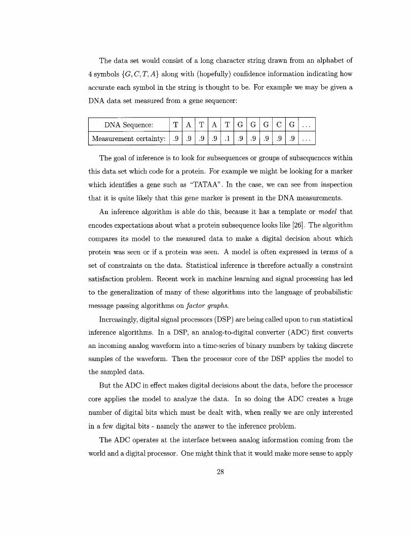
The data set would consist of a long character string drawn from an alphabet of
4 symbols {G, C, T, A} along with (hopefully) confidence information indicating how
accurate each symbol in the string is thought to be. For example we may be given a
DNA data set measured from a gene sequencer:
DNA Sequence: T A T A T G G G C G ...
Measurement certainty: .9 .9 .9 .9 .1 .9 .9 .9 .9 .9 ...
The goal of inference is to look for subsequences or groups of subsequences within
this data set which code for a protein. For example we might be looking for a marker
which identifies a gene such as "TATAA". In the case, we can see from inspection
that it is quite likely that this gene marker is present in the DNA measurements.
An inference algorithm is able do this, because it has a template or model that
encodes expectations about what a protein subsequence looks like [26]. The algorithm
compares its model to the measured data to make a digital decision about which
protein was seen or if a protein was seen. A model is often expressed in terms of a
set of constraints on the data. Statistical inference is therefore actually a constraint
satisfaction problem. Recent work in machine learning and signal processing has led
to the generalization of many of these algorithms into the language of probabilistic
message passing algorithms on factor graphs.
Increasingly, digital signal processors (DSP) are being called upon to run statistical
inference algorithms. In a DSP, an analog-to-digital converter (ADC) first converts
an incoming analog waveform into a time-series of binary numbers by taking discrete
samples of the waveform. Then the processor core of the DSP applies the model to
the sampled data.
But the ADC in effect makes digital decisions about the data, before the processor
core applies the model to analyze the data. In so doing the ADC creates a huge
number of digital bits which must be dealt with, when really we are only interested
in a few digital bits - namely the answer to the inference problem.
The ADC operates at the interface between analog information coming from the
world and a digital processor. One might think that it would make more sense to apply
the model before making digital decisions about it. We could envision a smarter ADC
which incorporates a model of the kind of signals it is likely to see into its conversion
process. Such an ADC could potentially produce a more accurate digital output while
consuming less resources. For example, in a radio receiver, we could model the effects
of the transmitter system on the signal such as compression, coding, and modulation
and the effect of the channel on the signal such as noise, multi-path, multiple access
interference (MAI), etc. We might hope that the performance of the ADC might then
scale with the descriptive power (compactness and generality) of our model.
1.3 Application: Wireless Transceivers
In practice replacing digital computers with an alternative computing paradigm is
a risky proposition. Alternative computing architectures, such as parallel digital
computers have not tended to be commercially viable, because Moore's Law has
persistently enabled conventional von Neumann architectures to render alternatives
unnecessary. Besides Moore's Law, digital computing also benefits from mature tools
and expertise for optimizing performance at all levels of the system: process technol-
ogy, fundamental circuits, layout and algorithms. Many engineers are simultaneously
working to improve every aspect of digital technology, while alternative technolo-
gies like analog computing do not have the same kind of industry juggernaut pushing
them forward. Therefore, if we want to show that analog, continuous-time, distributed
computing can be viable in practice, we must think very carefully about problems for
which it is ideally well-suited.
There is one application domain which has persistently resisted the allure of digital
scaling. High-speed analog circuits today are used in radios to create, direct, filter,
amplify and synchronize sinusoidal waveforms. Radio transceivers use oscillators to
produce sinusoids, resonant antenna structures to direct them, linear systems to filter
them, linear amplifiers to amplify them, and an oscillator or a phase-lock loop to
synchronize them. Analog circuits are so well-suited to these tasks in fact, that it is a
fairly recent development to use digital processors for such jobs, despite the incredible
advantages offered by the scalability and programmability of digital circuits. At lower
frequencies, digital processing of radio signals, called software radio is an important
emerging technology. But state-of-the-art analog circuits will always tend to be five to
ten times faster than the competing digital technology and use ten to a hundred times
less power. For example, at the time of writing, state-of-the-art analog circuits operate
at approximately 10Ghz while state-of-the-art digital operate at approximately 2GHz.
Radio frequency (RF) signals in wireless receivers demand the fastest possible signal
processing. Portable or distributed wireless receivers need to be small, inexpensive,
and operate on an extremely limited power budget. So despite the fast advance of
digital circuits, analog circuits have continued to be of use in radio front-ends.
Despite these continued advantages, analog circuits are quite limited in their com-
putational scope. Analog circuits have a difficult time producing or detecting arbi-
trary waveforms, because they are not programmable. Furthermore, analog circuit
design is limited in the types of computations it can perform compared to digital,
and in particular includes little notion of stochastic processes.
The unfortunate result of this inflexibility in analog circuitry is that radio trans-
mitters and receivers are designed to conform to industry standards. Wireless stan-
dards are costly and time-consuming to establish, and subject to continued obsoles-
cence. Meanwhile the Federal Communications Commission (FCC) is over-whelmed
by the necessity to perform top-down management of a menagerie of competing stan-
dards. It would be an important achievement to create radios that could adapt to
solve their local communications problems enabling bottom-up rather than top-down
management of bandwidth resources. A legal radio in such a scheme would not be one
that broadcasts within some particular frequency range and power level, but instead
would "play well with others". The enabling technology required for a revolution in
wireless communication is programmable statistical signal processing with the power,
cost and speed performance of state-of-the-art analog circuits.
1.4 Road-map: Statistical Signal Processing by Sim-
ple Physical Systems
When oscillators hang from separate beams, they will swing freely. But when oscil-
lators are even slightly coupled, such as by hanging them from the same beam, they
will tend to synchronize their respective phase. The moments when the oscillators
instantaneously stop and reverse direction will come to coincide. This is called en-
trainment and it is an extremely robust physical phenomena which occurs in both
coupled dissipative linear oscillators as well as coupled nonlinear systems.
One kind of statistical inference - statistical signal processing - involves estimating
parameters of a transmitter system when given a noisy version of the transmitted
signal. One can actually think of entraining oscillators as performing this kind of
task. One oscillator is making a decision about the phase of the other oscillator given
a noisy received signal.
Oscillators tend to be stable, efficient building blocks for engineering, because they
derive directly from the underlying physics. To borrow an analogy from computer
science, building an oscillator is like writing "native" code. The outcome tends to
execute very fast and efficiently, because we make direct use of the underlying hard-
ware. We are much better off using a few transistors to make a physical oscillator
than simulating an oscillator in a digital computer language running in an operating
system on a general purpose digital processor. And yet this circuitous approach is
precisely what a software radio does.
All of this might lead us to wonder if there is a way get the efficiency and elegance
of a native implementation combined with the flexibility of a more abstract implemen-
tation. Towards this end, this dissertation will show how to generalize a ring-oscillator
to produce native nonlinear dynamical systems which can be programmed to create,
filter, and synchronize arbitrary analog waveforms and to decode and estimate the
digital information carried by these waveforms. Such systems begin to bridge the gap
between the base-band statistical signal processing implemented in a digital signal
processor and analog RF circuits. Along the way, we learn how to understand the
synchronization of oscillators by entrainment as an optimum statistical estimation
algorithm.
The approach I took in developing this thesis was to first try to design oscilla-
tors which can create arbitrary waveforms. Then I tried to get such oscillators to
entrain. Finally I was able to find a principled way to generalize these oscillators to
perform general-purpose statistical signal processing by writing them in the language
of probabilistic message-passing on factor graphs.
1.5 Analog Continuous-Time Distributed Comput-
ing
The digital revolution with which we are all familiar is predicated upon the digital
abstraction, which allows us to think of computing in terms of logical operations on
zeros and ones (or bits) which can be represented in any suitable computing hardware.
The most common representation of bits, of course, is by high and low voltage values
in semiconductor integrated circuits.
The digital abstraction has provided wonderful benefits, but it comes at a cost;
The digital abstraction means discarding all of the state space available in the voltage
values between a low voltage and a high voltage. It also tends to discard geographical
information about where bits are located on a chip. Some bits are actually, physically
stored next to one another while other bits are stored far apart. The von Neumann
architecture requires that any bit is available with any other bit for logical combination
at any time; All bits must be accessible within one operational cycle. This is achieved
by imposing a clock and globally synchronous operation on the digital computer. In
an integrated circuit (a chip), there is an lower bound on the time it takes to access
the most distant bits. This sets the lower bound on how short a clock cycle can be.
If the clock were to switch faster than that, a distant bit might not arrive in time to
be processed before the next clock cycle begins.
But why should we bother? Moore's Law tells us that if we just wait, transis-
tors will get smaller and digital computers will eventually become powerful enough.
But Moore's Law is not a law at all, and digital circuits are bumping up against
the physical limits of their operation in nearly every parameter of interest: speed,
power consumption, heat dissipation, "clock-ability","simulate-ability" [17], and cost
of manufacture [451. One way to confront these limits is to challenge the digital ab-
straction and try to exploit the additional resources that we throw away when we use
what are inherently analog CT distributed circuits to perform digital computations.
If we make computers analog then we get to store on the order of 8 bits of information
where once we could only store a single bit. If we make computers asynchronous the
speed will no longer depend on worst case delays across the chip [12]. And if we make
use of geographical information by storing states next to the computations that use
them, then the clock can be faster or even non-existent [33]. The asynchronous logic
community has begun to understand these principles. Franklin writes,
"In clocked digital systems, speed and throughput is typically limited
by worst case delays associated with the slowest module in the system.
For asynchronous systems, however, system speed may be governed by
actual executing delays of modules, rather than their calculated worst
case delays, and improving predicted average delays of modules (even
those which are not the slowest) may often improve performance. In
general, more frequently used modules have greater influences on overall
performance [12]."
1.5.1 Analog VLSI Circuits for Statistical Inference
Probabilistic message-passing algorithms on factor graphs tend to be distributed,
asynchronous computations on continuous valued probabilities. They are therefore
well suited to "native" implementation in analog, continuous-time Very-Large-Scale-
Integrated (VLSI) circuitry. As Carver Mead predicted, and Loeliger and Lusten-
berger have further demonstrated, such analog VLSI implementations may promise
more than two orders of magnitude improvement in power consumption and silicon
area consumed [29].
The most common objection to analog computing is that digital computing is
much more robust to noise, but in fact all computing is sensitive to noise. Analog
computing is not robust because it never performs error correction in this way and so
tends to be more sensitive to noise. Digital computing avoids errors by performing
ubiquitous local error correction - every logic gate always thresholds its inputs to
Os and is even when it is not necessary. The approach advocated here and first
proposed by Loeliger, Lustenberger offers more "holographic" error correction; the
factor graph implemented by the circuit imposes constraints on the likely outputs
of the circuit. In addition, by representing all analog values differentially (with two
wires) and normalizing these values in each "soft-gate", there is a degree of ubiquitous
local error correction as well.
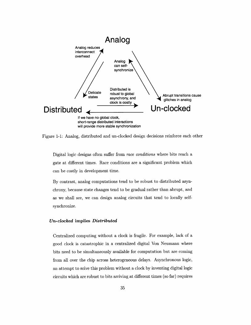
1.5.2 Analog, Un-clocked, Distributed
Philosophically it makes sense that if we are going to recover continuous degrees-of-
freedom in state we should also try to recover continuous degrees-of-freedom in time.
But it also seems that analog CT and distributed computing go hand in hand since
each of these design choices tends to reinforce the others. If we choose not to have
discrete states, we should also discard the requirement that states occur at discrete
times, and independently of geographical proximity.
Analog Circuits imply Un-clocked
Clocks tend to interfere with analog circuits. More generally, highly dis-
crete time steps are incompatible with analog state, because sharp state
transitions add glitches and noise to analog circuits.
Analog Circuits imply Distributed
Analog states are more delicate than digital states so they should not risk
greater noise corruption by travelling great distances on a chip.
Un-clocked implies Analog Circuits
AnalogAnalog reducesinterconnectoverhead
synchronize
/ a Distributed isDelicate robust to globalstates asynchrony, and
clock is costly
Distributed , *If we have no global clock,short-range distributed interactionswill provide more stable synchronization
Abrupt transitions causeglitches in analog
Un-clocked
Figure 1-1: Analog, distributed and un-clocked design decisions reinforce each other
Digital logic designs often suffer from race conditions where bits reach a
gate at different times. Race conditions are a significant problem which
can be costly in development time.
By contrast, analog computations tend to be robust to distributed asyn-
chrony, because state changes tend to be gradual rather than abrupt, and
as we shall see, we can design analog circuits that tend to locally self-
synchronize.
Un-clocked implies Distributed
Centralized computing without a clock is fragile. For example, lack of a
good clock is catastrophic in a centralized digital Von Neumann where
bits need to be simultaneously available for computation but are coming
from all over the chip across heterogeneous delays. Asynchronous logic,
an attempt to solve this problem without a clock by inventing digital logic
circuits which are robust to bits arriving at different times (so far) requires
impractical overhead in circuit complexity. Centralized digital computers
therefore need clocks.
We might try to imagine a centralized analog computer without a clock
using emergent synchronization via long-range interactions to synchronize
distant states with the central processor. But one of the most basic results
from control theory tells us that control systems with long delays have
poor stability. So distributed short-range distributed interactions are more
likely to result in stably synchronized computation. To summarize this
point: if there isn't a global synchronizing clock, then longer delays in the
system will lead to larger variances in timing inaccuracies.
Distributed weakly implies Analog Circuits
Distributed computation does not necessarily imply the necessity of ana-
log circuits. Traditional parallel computer architectures for example, are
collections of many digital processors. However, extremely fine grained
parallelism can often create a great deal of topological complexity for the
computer's interconnect compared to a centralized architecture with a
single shared bus. (A centralized bus is the definition of centralized com-
putation - it simplifies the topology but creates the so called von Neumann
"bottleneck").
For a given design, Rents Rule characterizes the relationship between the
amount of computational elements (e.g. logic blocks) and the number of
wires associated with the design. Rent's rule is
N = KGP, (1.1)
where N is the number of wires emanating from a region, G is the num-
ber of circuit components (or logic blocks), K is Rent's constant, and
p is Rent's exponent. Lower N means less area devoted to wiring. For
message passing algorithms on relatively "flat" graphs with mostly local
interconnections, we can expect p ~ 1. For a given amount of computa-
tional capacity G, the constant K (and therefore N) can be reduced by
perhaps half an order of magnitude by representing between 5 and 8 bits
of information on a single analog line instead of on a wide digital bus.
Distributed weakly implies Un-clocked
Distributed computation does not necessarily imply the necessity of un-
clocked operation. For example, parallel computers based on multiple Von
Neumann processor cores generally have either global clocks or several
local clocks. But a distributed architecture makes clocking less necessary
than in a centralized system and combined with the costliness of clocks,
this would tend to point toward their eventual elimination.
The clock tree in a modern digital processor is very expensive in terms
of power consumption and silicon area. The larger the area over which
the same clock is shared, the more costly and difficult it is to distribute
the clock signal. An extreme illustration of this is that global clocking
is nearing the point of physical impossibility. As Moore's law progresses,
digital computers are fast approaching the fundamental physical limit on
maximum global clock speeds imposed by the minimum time it takes for
a bit to traverse the entire chip travelling at the speed of light on a silicon
dielectric.
A distributed system, by definition, has a larger number of computational
cores than a centralized system. Fundamentally, each core need not be
synchronized to the others in order to compute, as long as they can share
information when necessary. Sharing data, communication between two
computing cores always in some sense requires synchrony. This thesis
demonstrates a very low-complexity system in which multiuser communi-
cation is achieved by the receiver adapting to the rate at which data is
sent, rather than by a shared clock. Given this technology, multiple cores
could share common channels to accomplish point-to-point communica-
tion without the aid of a global clock. In essence, processor cores could
act like nearby users in a cell phone network. The systems proposed here
make this thinkable.
Let us state clearly that this is not an argument against synchrony in
computing systems, just the opposite. Synchronization seems to increase
information sharing between physical systems. The generalization of syn-
chrony, coherence may even be a fundamental resource for computing,
although this is a topic for another thesis. The argument here is only that
coherence in the general sense may be achieved by systems in other ways
besides imposing an external clock.
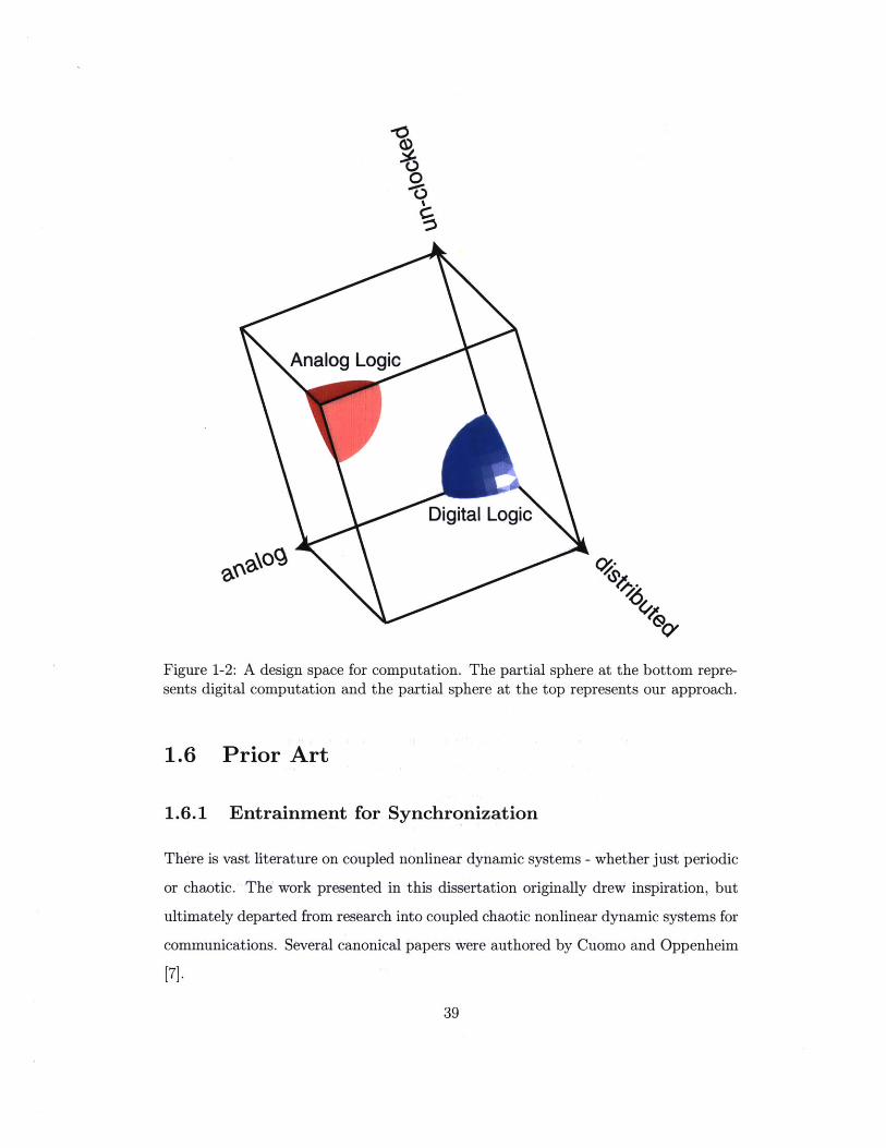
Imagine a three dimensional space with axes representing continuous (un-clocked)
vs. discrete (clocked) time, continuous (analog) vs. discrete (digital) state, and dis-
tributed vs. centralized computation. Conventional digital computing inhabits the
corner of the space where computing is digital, DT, and centralized. Digital com-
puting has been so successful and has so many resources driving its development,
that it competes extremely effectively against alternative approaches which are not
alternative enough. If we are trying to find a competitive alternative to digital com-
puting, chances are that we should try to explore parts of the space which are as
far as possible from the digital approach. So in retrospect, perhaps it should not
come as a surprise that we should make several simultaneous leaps of faith in order to
produce a compelling challenge to the prevailing digital paradigm. This thesis there-
fore moves away from several aspects of digital computing at once, simultaneously
becoming continuous state, CT, and highly distributed.
-0
0
Analog Logic
Digital Logic
Figure 1-2: A design space for computation. The partial sphere at the bottom repre-sents digital computation and the partial sphere at the top represents our approach.
1.6 Prior Art
1.6.1 Entrainment for Synchronization
There is vast literature on coupled nonlinear dynamic systems - whether just periodic
or chaotic. The work presented in this dissertation originally drew inspiration, but
ultimately departed from research into coupled chaotic nonlinear dynamic systems for
communications. Several canonical papers were authored by Cuomo and Oppenheim
[7].
This literature generally presents variations on the same theme. There is a trans-
mitter system of nonlinear first order ordinary differential equations. The transmitter
system can be arbitrarily divided into two subsystems, g and h,
dvdt g(v,w)
dw= h(v, w).dt
There is a receiver system which consists of one subsystem of the transmitter,
dw'd h(v,w')dt
The transmitter sends one or more of its state variables through a noisy channel
to the receiver. Entrainment of the receiver subsystem h to the transmitter system
will proceed to minimize the difference between the state of the transmitter, w and
the receiver w' at a rate
dAw'= J[h(v, w')] - Aw
dt
where J is the Jacobian of the subsystem, h and Aw = w - w'.
There is also an extensive literature on the control of chaotic nonlinear dynamical
systems. The basic idea there is essentially to push the system when it is close to
a bifurcation point to put it in one part of its state space or another. Recently,
there has been a rapidly growing number of chaotic communication schemes based
on exploiting these principles of chaotic synchronization and/or control [9]. Although
several researchers have been successful in implementing transmitters based on chaotic
circuits, the receivers in such schemes generally consist of some kind of matched filter.
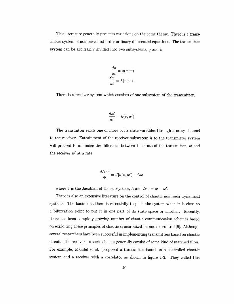
For example, Mandel et al. proposed a transmitter based on a controlled chaotic
system and a receiver with a correlator as shown in figure 1-3. They called this
Signal Out
Data
Correlatorr --- --Accumulator
Signal In Delay H Data
Figure 1-3: Chaotic communications system proposed by Mandal et al. [30]
scheme modified differential chaos shift keying (M-DCSK) [30].
Chaotic systems have some major disadvantages as engineering primitives for com-
munication systems. They are non-deterministic which makes it hard to control and
detect their signals. Chaotic systems are also not designable in that we do not have
a principled design methodology for producing a chaotic nonlinear dynamic system
which has particular desired properties such as conforming to a given spectral enve-
lope.
1.6.2 Neuromorphic and Translinear Circuits
Carver Mead first coined the term "neuromorphic" to mean implementing biolog-
ically inspired circuits in silicon. There is a long history and broad literature on
neuromorphic circuits including various kinds of artificial neural networks for vision
or speech processing as well as highly accurate silicon versions of biological neurons,
for example, implementing the frog's leg control circuitry.
In 1975, Barrie Gilbert coined the term translinear circuits to mean circuits that
use the inherent nonlinearity available from the full dynamic range of a semiconductor
junction. The most useful and disciplined approaches to neuromorphic circuits have
generally been based on translinear circuits. Applications of translinear circuits have
I .. I I- _- J_-. - - -- , , *1 -
included hearing aids and artificial cochlea (Sarpeshkar et al.), low level image process-
ing vision chips (Carver Mead et al., Dan Seligson at Intel), Viterbi error correction
decoders in disk drives (IBM, Loeliger et al., Hagenauer et al.), as well as multipliers
[21], oscillators, and filters for RF applications such as a PLL [35]. Translinear cir-
cuits have only recently been proposed for performing statistical inference. Loeliger
and Lustenberger have demonstrated BJT and sub-threshold CMOS translinear cir-
cuits which implement the sum-product algorithm in probabilistic graphical models
for soft error correction decoding [29]. Similar circuits were simultaneously proposed
by Hagenauer et al. [19] and are the subject of recent research by Dai [8].
1.6.3 Analog Decoders
When analog circuits settle to an equilibrium state, they minimize an energy or
action, although this is not commonly how the operation of analog circuits has been
understood. One example where this was made explicit, is based on Minty's elegant
solution to the shortest problem path problem. The decoding of a trellis code is
equivalent to the shortest path problem in a directed graph. Minty assumes a net of
flexible, variable length strings which form a scale model of an undirected graph in
which we must find the shortest path. If we hold the source node and the destination
node and pull the nodes apart until the net is tightened, we find the solution along
the tightened path.
"An analog circuit solution to the shortest-path problem in directed graph
models has been found independently by Davis and much later by Loeliger.
It consists of an analog network using series-connected diodes. Accord-
ing to the individual path section lengths, a number of series connected
diodes are placed. The current will then flow along the path with the least
number of series-connected, forward biased diodes. Note however that the
sum of the diode threshold voltages fundamentally limits practical applica-
tions. Very high supply voltages will be needed for larger diode networks,
which makes this elegant solution useless for VLSI implementations. [29]"
There is a long history and large literature on analog implementations of error
correction decoders. Lustenberger provides a more complete review of the field in
his doctoral thesis [291. He writes, "the new computationally demanding iterative
decoding techniques have in part driven the search for alternative implementations
of decoders." Although there had been much work on analog implementations of
the Viterbi algorithm [43], Wiberg et al. were the first to think about analog im-
plementations of the more general purpose sum-product algorithm. Hagenauer et al.
proposed the idea of an analog implementation approach for the maximum a poste-
riori (MAP) decoding algorithm, but apparently did not consider actual transistor
implementations.
1.7 Contributions
1.7.1 Reduced Complexity Synchronization of Codes
Continuous-Time Analog Circuits for Arbitrary Waveform Generation and
Synchronization
This thesis generally applies statistical estimation theory to the entrainment of dy-
namical systems. This research program resulted in
" Continuous-time dynamical systems that can produce designable arbitrary wave-
forms.
* Continuous-time dynamical systems that perform maximum-likelihood synchro-
nization with the arbitrary waveform generator.
* A principled methodology for the design of both from the theory of finite state
machines
Reduced-Complexity Trellis Decoder for Synchronization
By calculating joint messages on the shift graph formed from the state transition
constraints of any finite state machine, we derive a hierarchy of state estimators of
increasing complexity and accuracy.
Since convolutional and turbo codes employ finite state machines, this directly
suggests application to decoding. The method described shows us how to "dial a
knob" between quality of decoding versus computational complexity.
Low-Complexity Spread Spectrum Acquisition
I derive a probabilistic graphical model for performing maximum-likelihood estima-
tion of the phase of a spreading sequence generated by an LFSR. Performing the
sum-product algorithm on this graph performs improved spread spectrum acquisi-
tion in terms of acquisition time and tracking robustness when bench-marked against
conventional direct sequence spread spectrum acquisition techniques. Furthermore,
this system will readily lend itself to implementation with analog circuits offering
improvements in power and cost performance over existing implementations.
Low-Complexity Multiuser Detection
Using CT analog circuits to produce faster, lower power, or less expensive statistical
signal processing would be useful in a wide variety of applications. In this thesis,
I demonstrate analog circuits which perform acquisition and tracking of a spread
spectrum code and lay the groundwork for performing multiuser detection the same
class of circuits.
1.7.2 Theory of Continuous-Time Statistical Estimation
Injection Locking Performs Maximum-Likelihood Synchronization
Continuous-Time
not just soft logic but smooth logic - cont. time operation
1.7.3 New Circuits
Analog Memory: Circuits for Continuous-Time Analog State Storage
Programmability: Circuit for Analog Routing/Multiplexing, soft-MUX
Design Flow for Implementing Statistical Inference Algorithms with Continuous-
Time Analog Circuits
e Define data structure and constraints in language of factor graphs (MATLAB)
" Compile to circuits
e Layout or Program gate array
1.7.4 Probabilistic Message Routing
Learning Probabilistic Routing Tables in ad hoc Peer-to-Peer Networks
Using the Sum Product Algorithm
Propose "Routing" as a new method for low complexity approximation of
joint distributions in probabilistic message passing

:.-- . :- . ., :w, c~:--Me um- ,:nnsk:.r;nbri,:%.:,2.$w&i".is-: ->:-X.-;':- .:-- .'.:.--' -- 6:''i-:--:.' -:-Wer'-2-4-"'" i':-N"'--:- 6 - ,,'ViPl-ull's--le*-M''' -
Chapter 2
Probabilistic Message Passing on
Graphs
"I basically know of two principles for treating complicated systems in
simple ways; the first is the principle of modularity and the second is the
principle of abstraction. I am an apologist for computational probability
in machine learning, and particularly for graphical models and variational
methods, because I believe that probability theory implements these two
principles in deep and intriguing ways - namely through factorization and
through averaging. Exploiting these two mechanisms as fully as possible
seems to me to be the way forward in machine learning."
Michael I. Jordan Massachusetts Institute of Technology, 1997.
2.1 The Uses of Graphical Models
2.1.1 Graphical Models for Representing Probability Distri-
butions
When we have a probability distribution over one or two random variables, we often
draw it on axes as in figure 2-1, just as we might plot any function of one or two
variables. When more variables are involved in a probability distribution, we can-
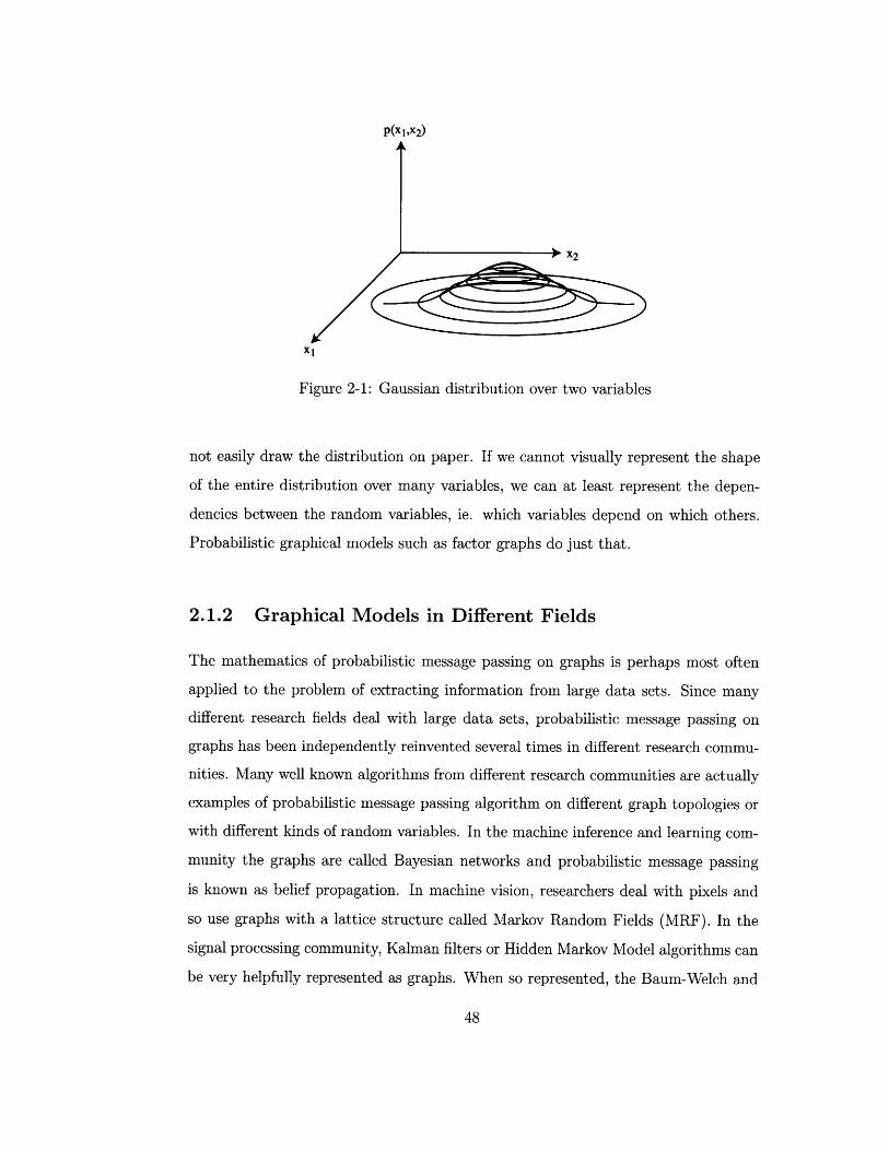
P(x 1,x2)A
X2
X1
Figure 2-1: Gaussian distribution over two variables
not easily draw the distribution on paper. If we cannot visually represent the shape
of the entire distribution over many variables, we can at least represent the depen-
dencies between the random variables, ie. which variables depend on which others.
Probabilistic graphical models such as factor graphs do just that.
2.1.2 Graphical Models in Different Fields
The mathematics of probabilistic message passing on graphs is perhaps most often
applied to the problem of extracting information from large data sets. Since many
different research fields deal with large data sets, probabilistic message passing on
graphs has been independently reinvented several times in different research commu-
nities. Many well known algorithms from different research communities are actually
examples of probabilistic message passing algorithm on different graph topologies or
with different kinds of random variables. In the machine inference and learning com-
munity the graphs are called Bayesian networks and probabilistic message passing
is known as belief propagation. In machine vision, researchers deal with pixels and
so use graphs with a lattice structure called Markov Random Fields (MRF). In the
signal processing community, Kalman filters or Hidden Markov Model algorithms can
be very helpfully represented as graphs. When so represented, the Baum-Welch and
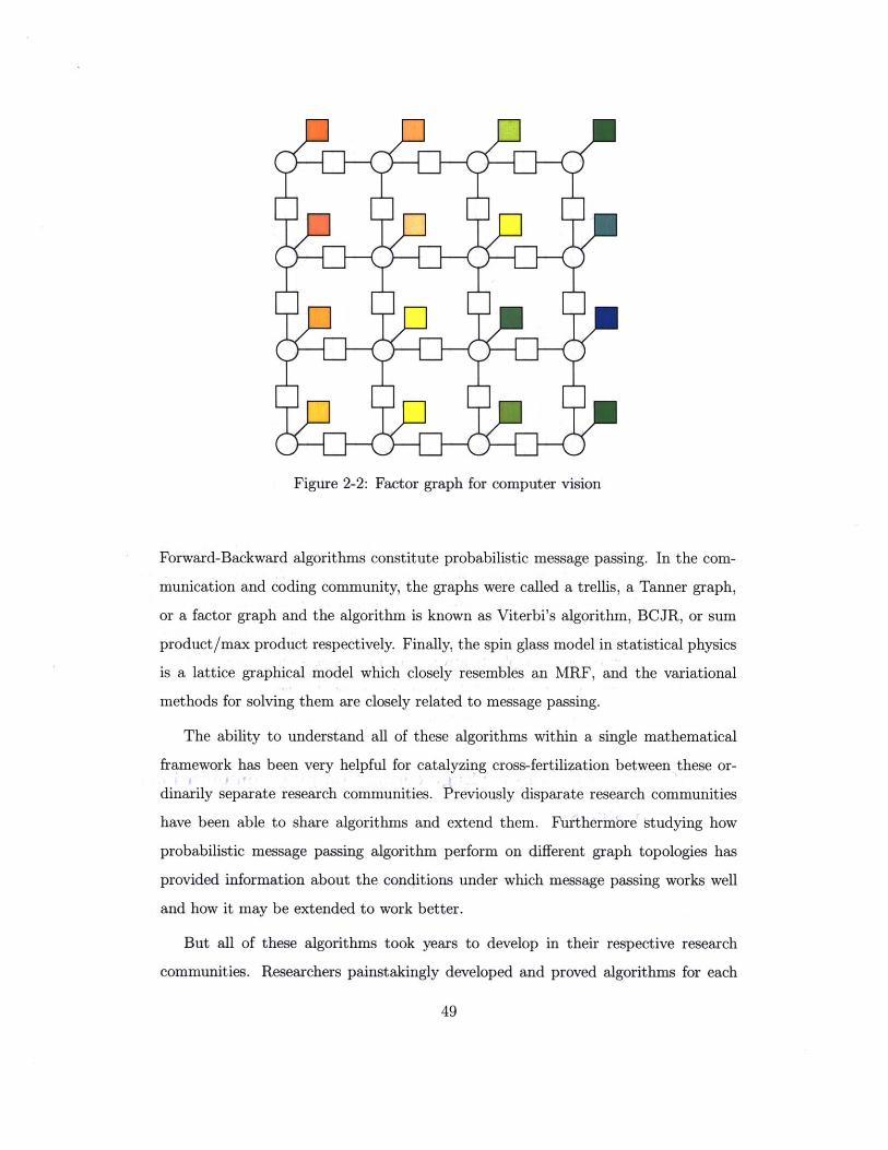
Figure 2-2: Factor graph for computer vision
Forward-Backward algorithms constitute probabilistic message passing. In the com-
munication and coding community, the graphs were called a trellis, a Tanner graph,
or a factor graph and the algorithm is known as Viterbi's algorithm, BCJR, or sum
product/max product respectively. Finally, the spin glass model in statistical physics
is a lattice graphical model which closely resembles an MRF, and the variational
methods for solving them are closely related to message passing.
The ability to understand all of these algorithms within a single mathematical
framework has been very helpful for catalyzing cross-fertilization between these or-
dinarily separate research communities. Previously disparate research communities
have been able to share algorithms and extend them. Furthermore studying how
probabilistic message passing algorithm perform on different graph topologies has
provided information about the conditions under which message passing works well
and how it may be extended to work better.
But all of these algorithms took years to develop in their respective research
communities. Researchers painstakingly developed and proved algorithms for each
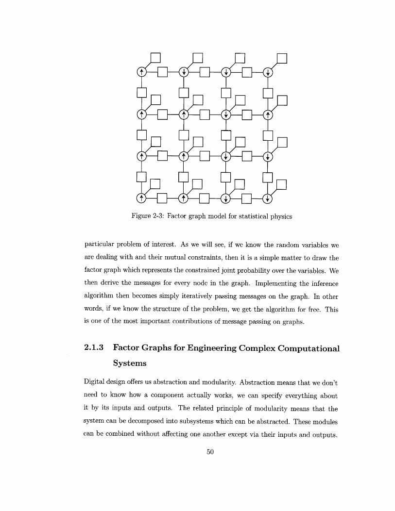
Figure 2-3: Factor graph model for statistical physics
particular problem of interest. As we will see, if we know the random variables we
are dealing with and their mutual constraints, then it is a simple matter to draw the
factor graph which represents the constrained joint probability over the variables. We
then derive the messages for every node in the graph. Implementing the inference
algorithm then becomes simply iteratively passing messages on the graph. In other
words, if we know the structure of the problem, we get the algorithm for free. This
is one of the most important contributions of message passing on graphs.
2.1.3 Factor Graphs for Engineering Complex Computational
Systems
Digital design offers us abstraction and modularity. Abstraction means that we don't
need to know how a component actually works, we can specify everything about
it by its inputs and outputs. The related principle of modularity means that the
system can be decomposed into subsystems which can be abstracted. These modules
can be combined without affecting one another except via their inputs and outputs.
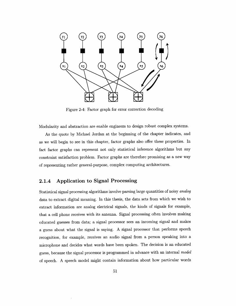
Figure 2-4: Factor graph for error correction decoding
Modularity and abstraction are enable engineers to design robust complex systems.
As the quote by Michael Jordan at the beginning of the chapter indicates, and
as we will begin to see in this chapter, factor graphs also offer these properties. In
fact factor graphs can represent not only statistical inference algorithms but any
constraint satisfaction problem. Factor graphs are therefore promising as a new way
of representing rather general-purpose, complex computing architectures.
2.1.4 Application to Signal Processing
Statistical signal processing algorithms involve parsing large quantities of noisy analog
data to extract digital meaning. In this thesis, the data sets from which we wish to
extract information are analog electrical signals, the kinds of signals for example,
that a cell phone receives with its antenna. Signal processing often involves making
educated guesses from data; a signal processor sees an incoming signal and makes
a guess about what the signal is saying. A signal processor that performs speech
recognition, for example, receives an audio signal from a person speaking into a
microphone and decides what words have been spoken. The decision is an educated
guess, because the signal processor is programmed in advance with an internal model
of speech. A speech model might contain information about how particular words
sound when they are spoken by different people and what kinds of sentences are
allowed in the English language [38]. The model encapsulates information such as,
you are more likely to see the words, "signal processing" in this document than you are
to see the words "Wolfgang Amadeus Mozart." Except of course, for the surprising
occurrence of the words "Wolfgang Amadeus Mozart" in the last sentence.
This kind of information, the relative likelihoods of occurrence of particular pat-
terns is expressed by the mathematics of probability theory. Probabilistic graphical
models provide a general framework for expressing the web of probabilities of a large
number of possible inter-related patterns that may occur in the data. Before we de-
scribe probabilistic graphical models, we will review some essentials of probabilities.
2.2 Review of the Mathematics of Probability
2.2.1 Expectations
The probability that a random value x falls between a and b is
Ibp(x)dx. (2.1)
An expectation is defined as
(f(x)) Jf()p(x)dx. (2.2)
The most trivial example of an expectation is the normalization condition where
f(x)=1,
(1) J p(x)dx = 1. (2.3)
Perhaps the most common expectation is the mean or first moment of a distribution,
= (x) = J xp(x)dx = 1. (2.4)
2.2.2 Bayes' Rule and Conditional Probability Distributions
Bayes' Rule,
p(xly) = XY) (2.5)p(y)
expresses the probability that event x occurs given that we know that event y occurred
in terms of the joint probability that both events occurred. The rule can be extended
to more than two variables. For example,
p(x,y,z) = p(Xly,z)p(y,z)
= p(xly, z)p(ylz)p(z)
= p(x,ylz)p(z). (2.6)
2.2.3 Independence, Correlation
If x and y are independent then, p(x, y) = p(x)p(y) and therefore p(zly) = p(x), since
by Bayes' rule, p(xly) = p(x, y)/p(y) p(x)p(y)/p(y) = p(x).
For uncorrelated variables, (xy) = (x)(y). Independent variables are always un-
correlated, but uncorrelated variables are not always independent. This is because
independence says there is NO underlying relationship between two variables and so
they must appear uncorrelated. By contrast,two variables which appear uncorrelated,
may still have some underlying causal connection.
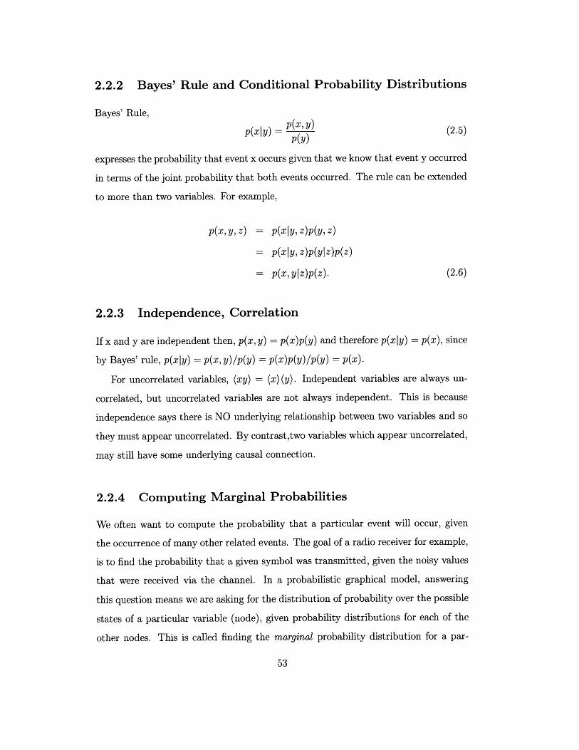
2.2.4 Computing Marginal Probabilities
We often want to compute the probability that a particular event will occur, given
the occurrence of many other related events. The goal of a radio receiver for example,
is to find the probability that a given symbol was transmitted, given the noisy values
that were received via the channel. In a probabilistic graphical model, answering
this question means we are asking for the distribution of probability over the possible
states of a particular variable (node), given probability distributions for each of the
other nodes. This is called finding the marginal probability distribution for a par-
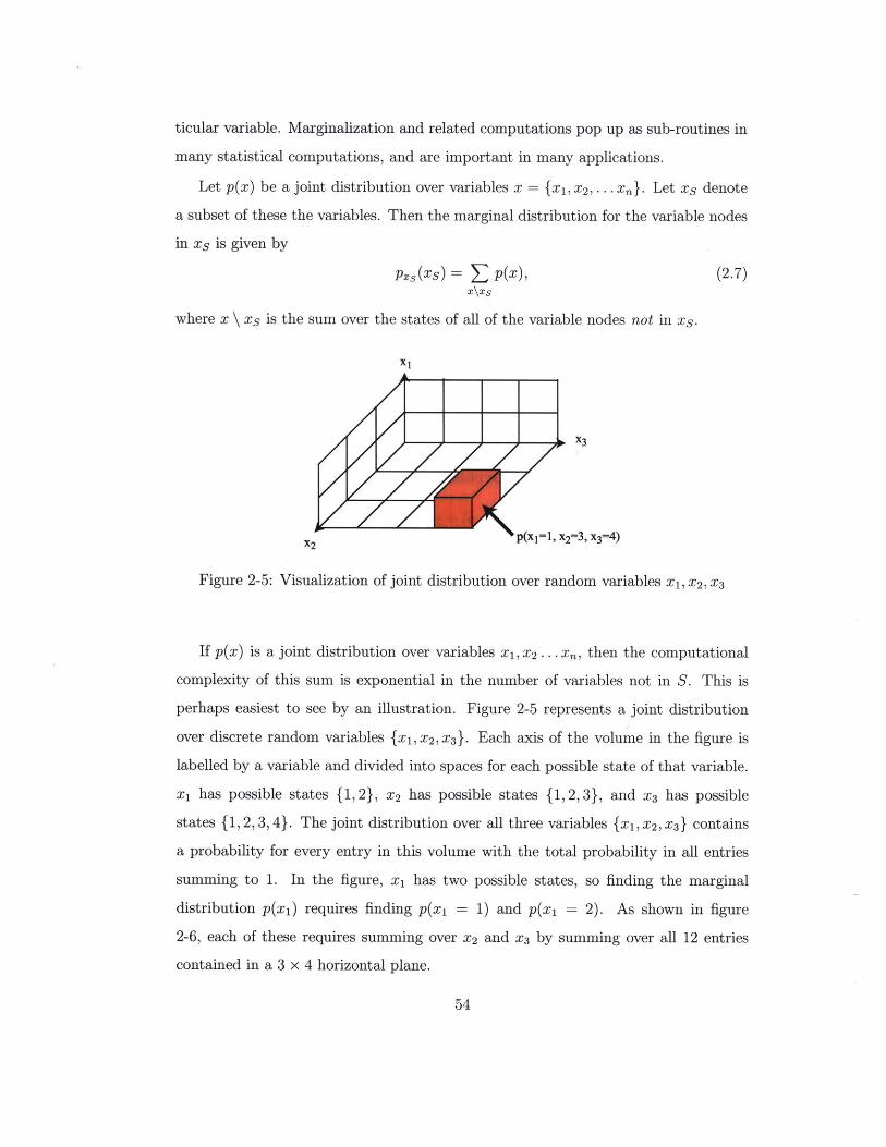
ticular variable. Marginalization and related computations pop up as sub-routines in
many statistical computations, and are important in many applications.
Let p(x) be a joint distribution over variables x = {Xi, x2 ,... xn}. Let xs denote
a subset of these the variables. Then the marginal distribution for the variable nodes
in xs is given by
PXs(Xs) = S p(x), (2.7)x\xs
where x \ xs is the sum over the states of all of the variable nodes not in xs.
X1
X3
P(X1=1, X2=3, x3=4)
Figure 2-5: Visualization of joint distribution over random variables X1 , x 2 , x 3
If p(x) is a joint distribution over variables X1 , X2 ... Xn, then the computational
complexity of this sum is exponential in the number of variables not in S. This is
perhaps easiest to see by an illustration. Figure 2-5 represents a joint distribution
over discrete random variables {X1 , x 2 , X3 }. Each axis of the volume in the figure is
labelled by a variable and divided into spaces for each possible state of that variable.
xi has possible states {1, 2}, x 2 has possible states {1, 2, 3}, and X3 has possible
states {1, 2, 3, 4}. The joint distribution over all three variables {X1 , x 2 , X3 } contains
a probability for every entry in this volume with the total probability in all entries
summing to 1. In the figure, xi has two possible states, so finding the marginal
distribution p(xi) requires finding p(x1 = 1) and p(x1 = 2). As shown in figure
2-6, each of these requires summing over x 2 and X3 by summing over all 12 entries
contained in a 3 x 4 horizontal plane.
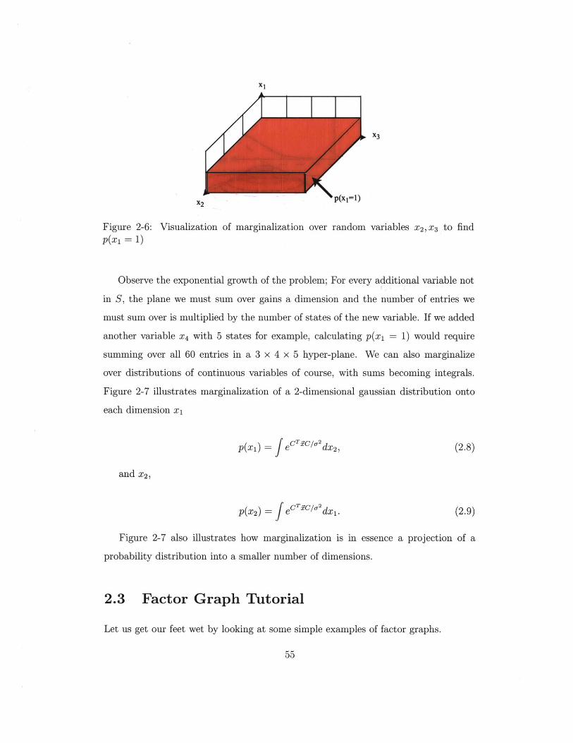
p(x=1)
Figure 2-6: Visualization of marginalization over random variables X2, X3 to findp(x1 = 1)
Observe the exponential growth of the problem; For every additional variable not
in S, the plane we must sum over gains a dimension and the number of entries we
must sum over is multiplied by the number of states of the new variable. If we added
another variable X4 with 5 states for example, calculating p(xi = 1) would require
summing over all 60 entries in a 3 x 4 x 5 hyper-plane. We can also marginalize
over distributions of continuous variables of course, with sums becoming integrals.
Figure 2-7 illustrates marginalization of a 2-dimensional gaussian distribution onto
each dimension x1
p(x1) = eCT IC/I2 dx 2, (2.8)
and X2,
p(x2) = ecTsc/A2dx1. (2.9)
Figure 2-7 also illustrates how marginalization is in essence a projection of a
probability distribution into a smaller number of dimensions.
2.3 Factor Graph Tutorial
Let us get our feet wet by looking at some simple examples of factor graphs.
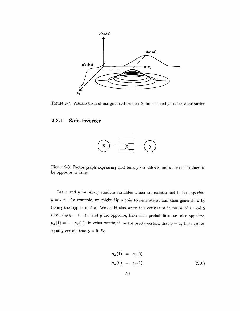
P(x 1,x2)
P(X2|X1)
P(X1|IX2) 4 X2
11
Figure 2-7: Visualization of marginalization over 2-dimensional gaussian distribution
2.3.1 Soft-Inverter
Figure 2-8: Factor graph expressing that binary variables x and y are constrained tobe opposite in value
Let x and y be binary random variables which are constrained to be opposites
y =~ x. For example, we might flip a coin to generate x, and then generate y by
taking the opposite of x. We could also write this constraint in terms of a mod 2
sum, x E y = 1. If x and y are opposite, then their probabilities are also opposite,
Px(1) = 1 - py(1). In other words, if we are pretty certain that x = 1, then we are
equally certain that y = 0. So,
Px i) = Py(0)
Px (0) = py (1). (2.10)
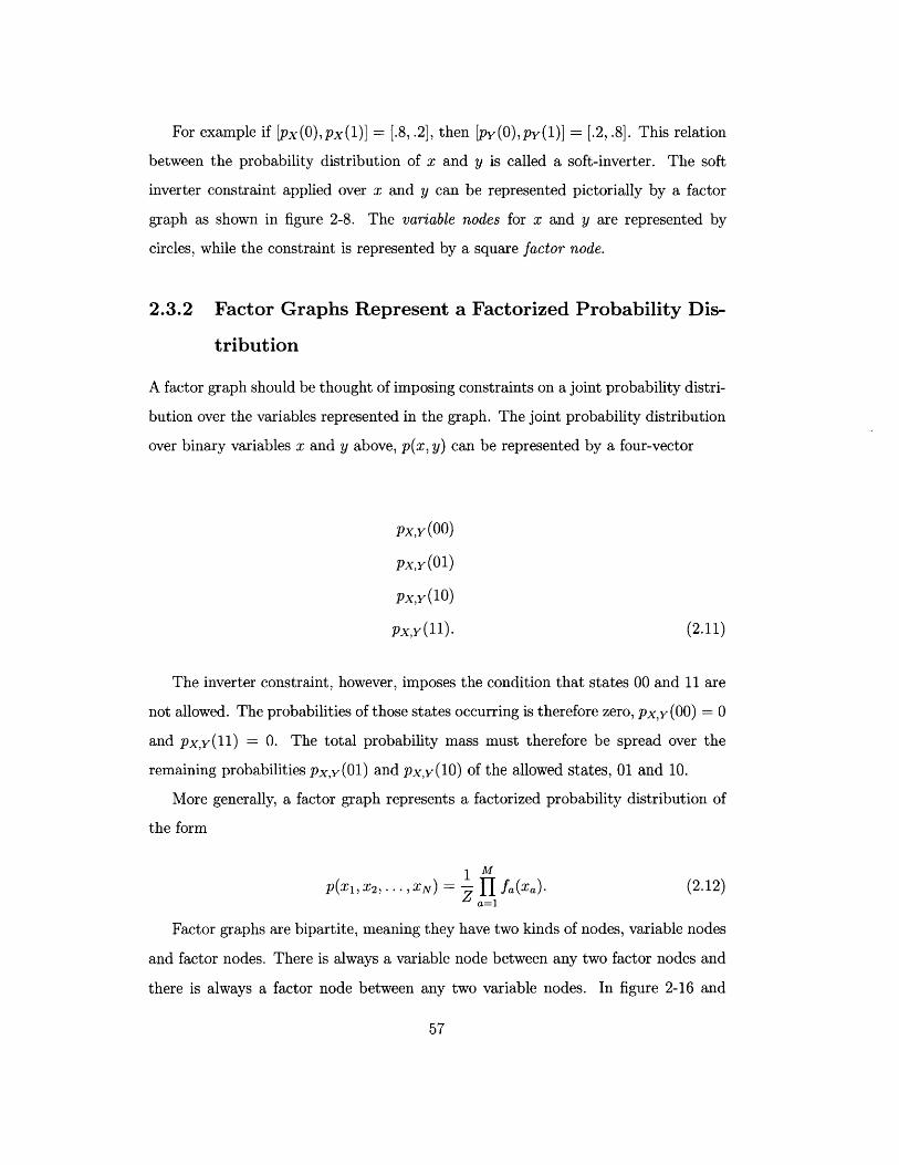
For example if [px(0),px(1)] = [.8, .2], then [py(O),py(l)] = [.2, .8]. This relation
between the probability distribution of x and y is called a soft-inverter. The soft
inverter constraint applied over x and y can be represented pictorially by a factor
graph as shown in figure 2-8. The variable nodes for x and y are represented by
circles, while the constraint is represented by a square factor node.
2.3.2 Factor Graphs Represent a Factorized Probability Dis-
tribution
A factor graph should be thought of imposing constraints on a joint probability distri-
bution over the variables represented in the graph. The joint probability distribution
over binary variables x and y above, p(x, y) can be represented by a four-vector
Px,Y (00)
PXY (01)
Px,y(10)
pX,y(11). (2.11)
The inverter constraint, however, imposes the condition that states 00 and 11 are
not allowed. The probabilities of those states occurring is therefore zero, px,y(00) = 0
and px,y(11) = 0. The total probability mass must therefore be spread over the
remaining probabilities px,y(01) and px,y(10) of the allowed states, 01 and 10.
More generally, a factor graph represents a factorized probability distribution of
the form
P(XlX2 ... XN) Z l fa(Xa). (2.12)1
Factor graphs are bipartite, meaning they have two kinds of nodes, variable nodes
and factor nodes. There is always a variable node between any two factor nodes and
there is always a factor node between any two variable nodes. In figure 2-16 and
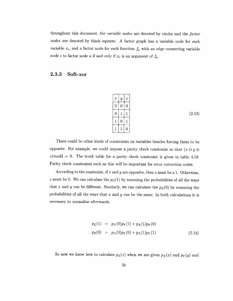
throughout this document, the variable nodes are denoted by circles and the factor
nodes are denoted by black squares. A factor graph has a variable node for each
variable xi, and a factor node for each function fa with an edge connecting variable
node i to factor node a if and only if x is an argument of fa.
2.3.3 Soft-xor
0 0 01
0 1 1 (2.13)
1 0 1
1 1 0
There could be other kinds of constraints on variables besides forcing them to be
opposite. For example, we could impose a parity check constraint so that (x G y Ez)mod2 = 0. The truth table for a parity check constraint is given in table 4.19.
Parity check constraints such as this will be important for error correction codes.
According to the constraint, if x and y are opposite, then z must be a 1. Otherwise,
z must be 0. We can calculate the pz(1) by summing the probabilities of all the ways
that x and y can be different. Similarly, we can calculate the pz(0) by summing the
probabilities of all the ways that x and y can be the same. In both calculations it is
necessary to normalize afterwards.
pz(1) = px(O)py(1)+px(1)py(0)
pz(0) = px(O)py(0)+px(1)py(1) (2.14)
So now we know how to calculate pz(z) when we are given px(x) and py(y) and
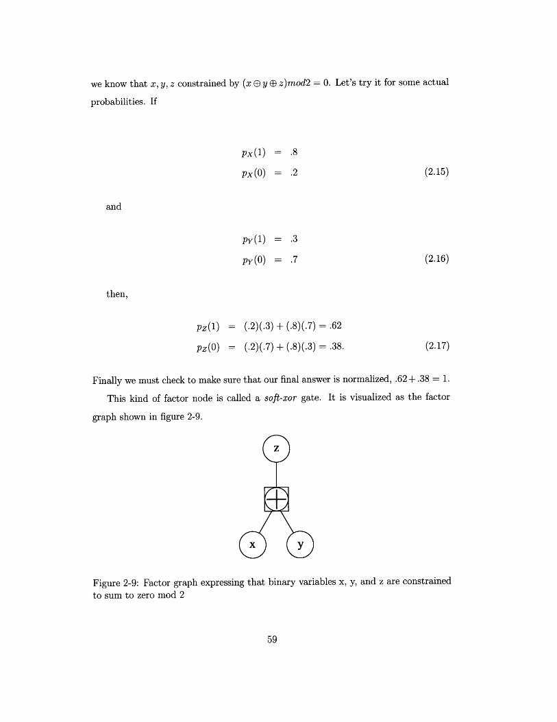
we know that x, y, z constrained by (x E y D z)mod2 = 0. Let's try it for some actual
probabilities. If
Px(1) = .8
px(0) = .2 (2.15)
and
py(1)
py(0)
then,
Pz(1)
Pz(O)
= (.2)(.3) + (.8)(.7) = .62
= (.2)(.7) + (.8)(.3) = .38. (2.17)
(2.16)
Finally we must check to make sure that our final answer is normalized, .62 +.38 = 1.
This kind of factor node is called a soft-xor gate. It is visualized as the factor
graph shown in figure 2-9.
Figure 2-9: Factor graph expressing that binary variables x, y, and z are constrained
to sum to zero mod 2
2.3.4 General Soft-gates
We appealed to a specialized arguments to derive the soft-inverter and soft-xor. But
more generally, one way we can think of soft-gates is as the probabilistic equivalent
of logic gates. For example, the soft-xor is the probability version of the logical XOR
function. Thought of this way, the output from a soft-gate tells us how likely it would
be for a distribution of input strings to satisfy its corresponding logic gate.
In fact, given any logic gate there is a principled way to find the output of the
corresponding soft-gate. The output from a soft-gate over three variables x, y, z is
given in general by
pz(z) = Y S px(x)py (y)f(x, y, z) (2.18)xEX yEY
where f(x, y, z) is the constraint function within a delta function which we will con-
sider to be zero except when its argument is true. If we substitute the constraint
function for the XOR, f(x, y, z) = 6(x e y G z = 0) into equation (2.18), we find that
pz(1) = S px(x)py(y)6(xey E1 =0)x,y={O,1}
pz(0) = E px(x)py(y)6(Xy e0=0) (2.19)x,y={O,1}
To calculate pz(I), we sum over all possible (binary) values of x and y. The constraint
within a dirac delta serves to include some probability terms and exclude others. So
in calculating pz(1), the px(0)py(1) and px(1)py(0) terms are included because
o(0 e Ie 1 =0) 1
J(1 e 0 E 1 =0) 1. (2.20)
While the px(O)py(0) and px(1)py(1) terms are zero because
J(0 E 0 E 1 0) 0
6(1 e 1 e 1 =0) =0. (2.21)
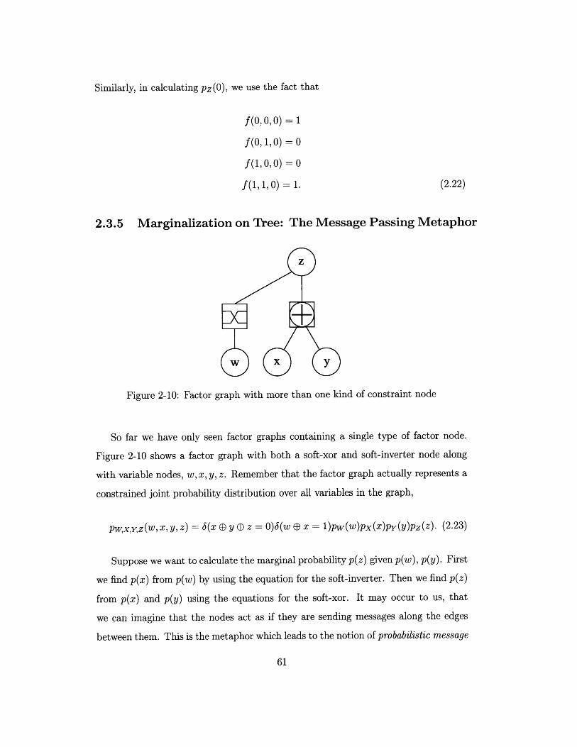
Similarly, in calculating pz(0), we use the fact that
f(0, 0,0) = 1
f(0,1,0) = 0
f(1, 0, 0) = 0
f(1,1,0) 1. (2.22)
2.3.5 Marginalization on Tree: The Message Passing Metaphor
z
w x y
Figure 2-10: Factor graph with more than one kind of constraint node
So far we have only seen factor graphs containing a single type of factor node.
Figure 2-10 shows a factor graph with both a soft-xor and soft-inverter node along
with variable nodes, w, x, y, z. Remember that the factor graph actually represents a
constrained joint probability distribution over all variables in the graph,
pw,x,y,z(w, X, y, z) = 6(x y ED z = 0)6(w D x = 1)pw(w)px(x)py(y)pz(z). (2.23)
Suppose we want to calculate the marginal probability p(z) given p(w), p(y). First
we find p(x) from p(w) by using the equation for the soft-inverter. Then we find p(z)
from p(x) and p(y) using the equations for the soft-xor. It may occur to us, that
we can imagine that the nodes act as if they are sending messages along the edges
between them. This is the metaphor which leads to the notion of probabilistic message
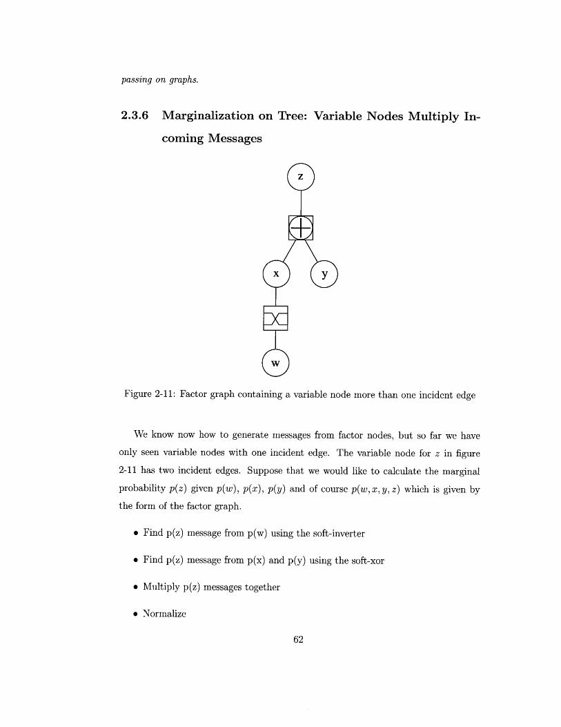
passing on graphs.
2.3.6 Marginalization on Tree: Variable Nodes Multiply In-
coming Messages
Figure 2-11: Factor graph containing a variable node more than one incident edge
We know now how to generate messages from factor nodes, but so far we have
only seen variable nodes with one incident edge. The variable node for z in figure
2-11 has two incident edges. Suppose that we would like to calculate the marginal
probability p(z) given p(w), p(x), p(y) and of course p(w, x, y, z) which is given by
the form of the factor graph.
* Find p(z) message from p(w) using the soft-inverter
" Find p(z) message from p(x) and p(y) using the soft-xor
* Multiply p(z) messages together
* Normalize
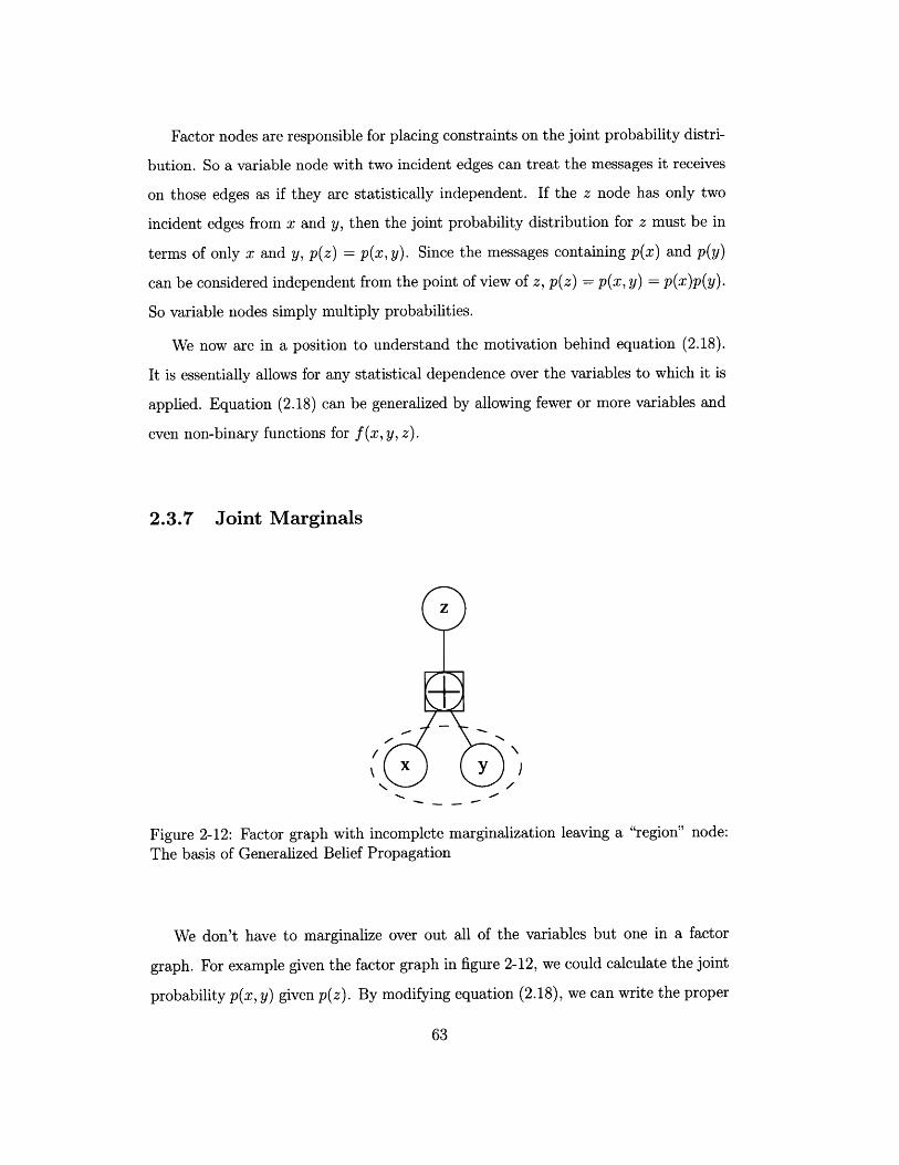
Factor nodes are responsible for placing constraints on the joint probability distri-
bution. So a variable node with two incident edges can treat the messages it receives
on those edges as if they are statistically independent. If the z node has only two
incident edges from x and y, then the joint probability distribution for z must be in
terms of only x and y, p(z) = p(x, y). Since the messages containing p(x) and p(y)
can be considered independent from the point of view of z, p(z) = p(x, y) = p(x)p(y).
So variable nodes simply multiply probabilities.
We now are in a position to understand the motivation behind equation (2.18).
It is essentially allows for any statistical dependence over the variables to which it is
applied. Equation (2.18) can be generalized by allowing fewer or more variables and
even non-binary functions for f(x, y, z).
2.3.7 Joint Marginals
z
X y
Figure 2-12: Factor graph with incomplete marginalization leaving a "region" node:The basis of Generalized Belief Propagation
We don't have to marginalize over out all of the variables but one in a factor
graph. For example given the factor graph in figure 2-12, we could calculate the joint
probability p(x, y) given p(z). By modifying equation (2.18), we can write the proper
message for p(x, y)
px,y (x, y) = - S pz(z)f (x, y, z). (2.24)zEZ
So that,
px,y(0,0) = pz(0)
px,y(O,1) = Pz(1)
px,y (1, 0) = pz(1)
px,y(1, 1) = pz(0). (2.25)
It is important to note that the probability distribution px,y(x, y) requires us to store
four numbers. It contains twice as much data than p(x) or p(y) alone. If we had a
joint probability distribution over three binary variables, for example px,y,z(x, y, z) it
would contain eight numbers. Each additional variable in a joint distribution increases
the size of the data structure exponentially. This is the essential idea in generalized
belief propagation (GBP) [56]. In GBP we form "region" nodes which represent joint
probabilities over more than one variable. We can perform message passing between
these new region nodes just as we would on any factor graph, at the expense of
exponentially increasing the computational complexity of the algorithm. GBP has a
number of uses. In this document we will show a novel way to use GBP to effectively
trade-off the quality of statistical estimates in a decoder against the computational
complexity of decoding. GBP can also be used to improve the answers that we get
from message passing on graphs with cycles.
2.3.8 Graphs with Cycles
So far, all of the graphs we have examined have had a tree topology. For graphs that
are trees, probabilistic message passing is guaranteed to give us the correct answers
for the marginal probability or joint marginal probability of any variables in the
graph. Graphs with cycles ("loopy graphs") are a different story. Message passing
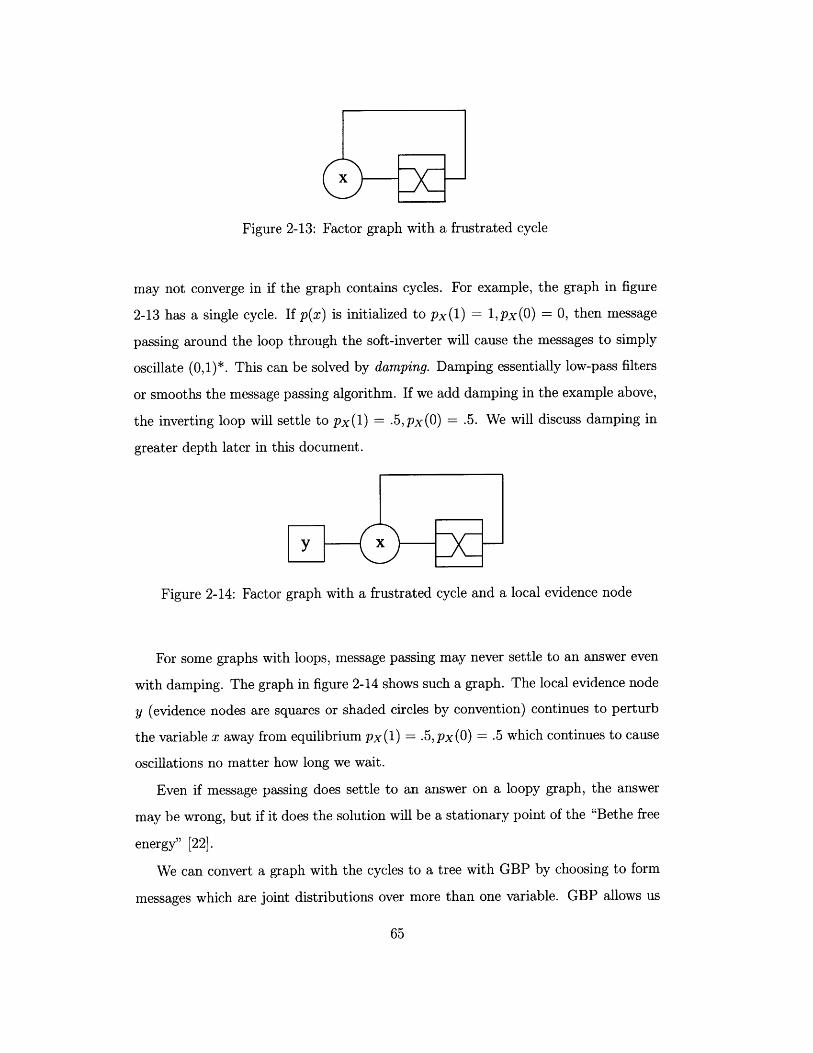
Figure 2-13: Factor graph with a frustrated cycle
may not converge in if the graph contains cycles. For example, the graph in figure
2-13 has a single cycle. If p(x) is initialized to px(1) = 1,px(O) = 0, then message
passing around the loop through the soft-inverter will cause the messages to simply
oscillate (0,1)*. This can be solved by damping. Damping essentially low-pass filters
or smooths the message passing algorithm. If we add damping in the example above,
the inverting loop will settle to px(1) = .5,px(O) = .5. We will discuss damping in
greater depth later in this document.
Figure 2-14: Factor graph with a frustrated cycle and a local evidence node
For some graphs with loops, message passing may never settle to an answer even
with damping. The graph in figure 2-14 shows such a graph. The local evidence node
y (evidence nodes are squares or shaded circles by convention) continues to perturb
the variable x away from equilibrium px(1) = .5, px(0) = .5 which continues to cause
oscillations no matter how long we wait.
Even if message passing does settle to an answer on a loopy graph, the answer
may be wrong, but if it does the solution will be a stationary point of the "Bethe free
energy" [22].
We can convert a graph with the cycles to a tree with GBP by choosing to form
messages which are joint distributions over more than one variable. GBP allows us
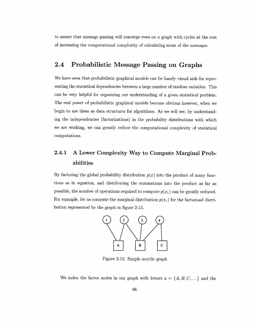
to assure that message passing will converge even on a graph with cycles at the cost
of increasing the computational complexity of calculating some of the messages.
2.4 Probabilistic Message Passing on Graphs
We have seen that probabilistic graphical models can be handy visual aids for repre-
senting the statistical dependencies between a large number of random variables. This
can be very helpful for organizing our understanding of a given statistical problem.
The real power of probabilistic graphical models become obvious however, when we
begin to use them as data structures for algorithms. As we will see, by understand-
ing the independencies (factorizations) in the probability distributions with which
we are working, we can greatly reduce the computational complexity of statistical
computations.
2.4.1 A Lower Complexity Way to Compute Marginal Prob-
abilities
By factoring the global probability distribution p(x) into the product of many func-
tions as in equation, and distributing the summations into the product as far as
possible, the number of operations required to compute p(xi) can be greatly reduced.
For example, let us compute the marginal distribution p(xi) for the factorized distri-
bution represented by the graph in figure 2-15.
1 2 3 4
A XBC
Figure 2-15: Simple acyclic graph
We index the factor nodes in our graph with letters a = {A, B, C, .. .} and the
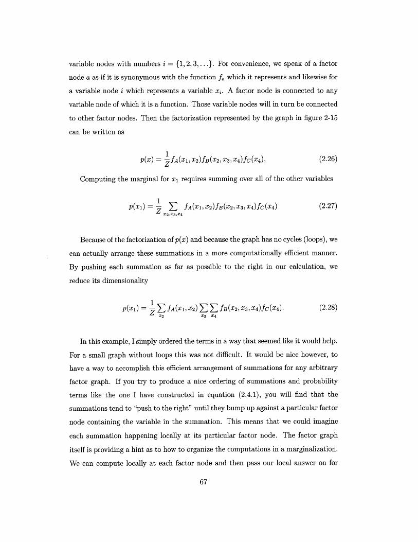
variable nodes with numbers i = {1, 2, 3, ... }. For convenience, we speak of a factor
node a as if it is synonymous with the function fa which it represents and likewise for
a variable node i which represents a variable xi. A factor node is connected to any
variable node of which it is a function. Those variable nodes will in turn be connected
to other factor nodes. Then the factorization represented by the graph in figure 2-15
can be written as
1p(x) -fA(x1, x2)fB (X2, X3, X4)fC(X4) (2.26)Z
Computing the marginal for x1 requires summing over all of the other variables
p(x1) = 1 S fA(Xi,x2)fB(X2,X3,x4)fC(x4) (2.27)X2,X3,X4
Because of the factorization of p(x) and because the graph has no cycles (loops), we
can actually arrange these summations in a more computationally efficient manner.
By pushing each summation as far as possible to the right in our calculation, we
reduce its dimensionality
p(x1 )= I fA(x1,x 2 ) fB (X2,3,4)fC(4)- (2.28)X2 X3 X4
In this example, I simply ordered the terms in a way that seemed like it would help.
For a small graph without loops this was not difficult. It would be nice however, to
have a way to accomplish this efficient arrangement of summations for any arbitrary
factor graph. If you try to produce a nice ordering of summations and probability
terms like the one I have constructed in equation (2.4.1), you will find that the
summations tend to "push to the right" until they bump up against a particular factor
node containing the variable in the summation. This means that we could imagine
each summation happening locally at its particular factor node. The factor graph
itself is providing a hint as to how to organize the computations in a marginalization.
We can compute locally at each factor node and then pass our local answer on for
aggregation into the final answer. This is known as a probabilistic message passing
algorithm.
Many statistical computations are like marginalization in the sense that they
require computation over a factored joint distribution to compute a statistic of interest
on a subset of variables and therefore lend themselves to a distributed message passing
approach. First we show how to perform marginalization by probabilistic message
passing. This is often called the sum product algorithm.
2.4.2 The Sum-Product Algorithm
Let us continue to suppose that we want to find the marginal probability distribution
p(x1 ) on the graph in figure 2-15. In many applications we deal with random variables
which are described by a discrete probability distribution, so the marginal distribution
for a variable node is actually a vector representing the relative probabilities that
variable i is in each of its various possible states. The message nia(xi) from a
variable node i to a factor node a is also a vector containing the relative probabilities
of the states of variable i given all the information available to node i except the
information from the factor node fa
ni-*a(Xi) = J mb-i(xi). (2.29)bEN(i)\a
Similarly, the message mai (xi) from a factor node fa to a neighboring variable node
i is a vector containing the relative probabilities of the states of variable i given the
information available to fa
ma-i (Xi) =E fa (Xa) n ny (Xi). (2.30)xa\xi jcN(a)\i
Using the message passing rules we see that
pi(x 1 ) oc mA,1(x1)
oc 1 fA(x1, X2) n2-A(X2)X2
oc E fA(Xi, X2)mB-+2(X2)X2
oc E fA(i, X 2) f (2, X3 , 4)n3- (3)n4--B(X4)X2 X3 X4
oc fA(z1, X 2) E E fB( 2, x 3, X4)MC-4 (x4)X2 X3 X4
oc 5 fA(X1, x2) 5 5 fA(x2, X3, X4)fc(X2, x4) (2.31)X2 X3 X4
which is exactly the desired marginal distribution.
The sum product algorithm provides a general method for computing marginal
probability efficiently in this way. It iterates on local estimates of the marginal prob-
abilities of the variables by using probability information only from neighboring (con-
nected) factor nodes. Nodes are said to share information with adjacent nodes by
"passing a message" along the edge that connects them. Although messages are
only passed between neighboring nodes of the graph at each step of the algorithm,
over many steps information can traverse the graph in an attempt to find a globally
consistent estimate of the marginal probabilities.
Message passing is a kind of dynamic programming, storing intermediate approx-
imations to the true marginals and iterating on them. If the graph has no cycles,
the sum product algorithm will find the exact maximum likelihood estimate for the
marginal probability distributions for the state variables and is guaranteed to con-
verge. If a graph is "loopy" (has cycles), as in our coding example, then the messages
can potentially continue to traverse the graph forever searching in vain for a globally
consistent answer and the algorithm may never converge. In practice, however, the
sum product algorithm will often arrive at a good approximation of the exact marginal
distributions even on loopy graphs. Much recent work has been centered on under-
standing under what circumstances this is so and the accuracy of the approximations
made by the sum product and related algorithms.
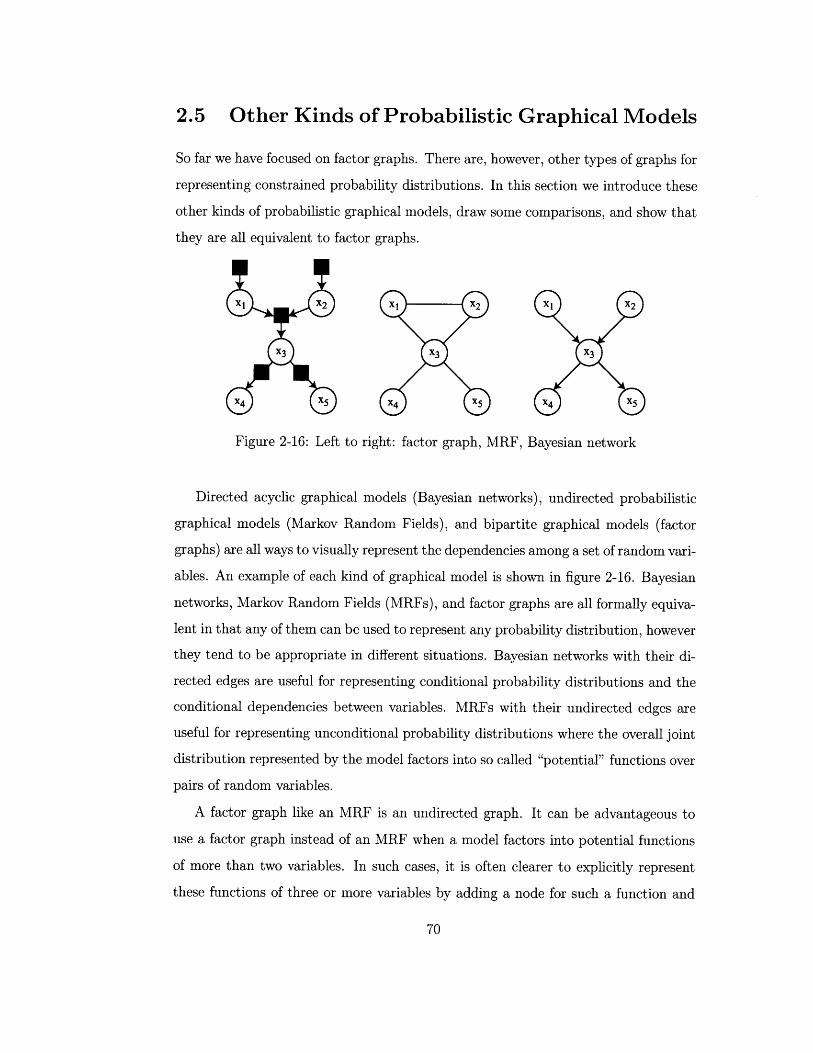
2.5 Other Kinds of Probabilistic Graphical Models
So far we have focused on factor graphs. There are, however, other types of graphs for
representing constrained probability distributions. In this section we introduce these
other kinds of probabilistic graphical models, draw some comparisons, and show that
they are all equivalent to factor graphs.
X1 X2 X1 X2 X1 X2
X3 X3 X3
X4 X4 X5 X4 X5
Figure 2-16: Left to right: factor graph, MRF, Bayesian network
Directed acyclic graphical models (Bayesian networks), undirected probabilistic
graphical models (Markov Random Fields), and bipartite graphical models (factor
graphs) are all ways to visually represent the dependencies among a set of random vari-
ables. An example of each kind of graphical model is shown in figure 2-16. Bayesian
networks, Markov Random Fields (MRFs), and factor graphs are all formally equiva-
lent in that any of them can be used to represent any probability distribution, however
they tend to be appropriate in different situations. Bayesian networks with their di-
rected edges are useful for representing conditional probability distributions and the
conditional dependencies between variables. MRFs with their undirected edges are
useful for representing unconditional probability distributions where the overall joint
distribution represented by the model factors into so called "potential" functions over
pairs of random variables.
A factor graph like an MRF is an undirected graph. It can be advantageous to
use a factor graph instead of an MRF when a model factors into potential functions
of more than two variables. In such cases, it is often clearer to explicitly represent
these functions of three or more variables by adding a node for such a function and
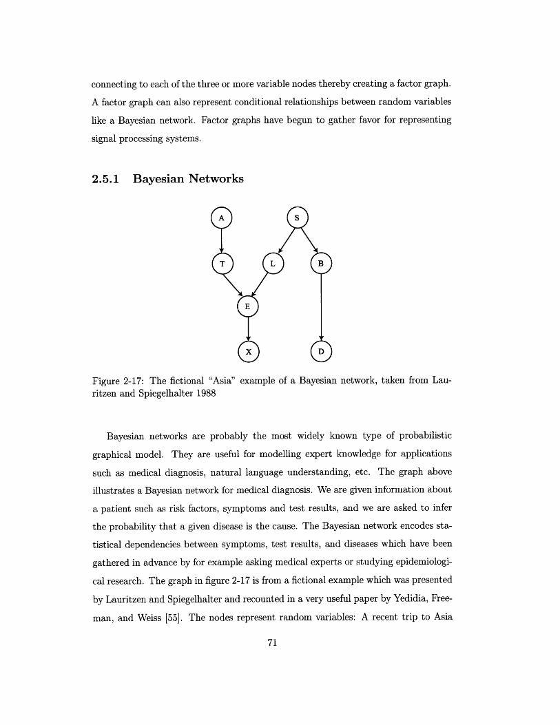
connecting to each of the three or more variable nodes thereby creating a factor graph.
A factor graph can also represent conditional relationships between random variables
like a Bayesian network. Factor graphs have begun to gather favor for representing
signal processing systems.
2.5.1 Bayesian Networks
A S
T L B
E
X D
Figure 2-17: The fictional "Asia" example of a Bayesian network, taken from Lau-ritzen and Spiegelhalter 1988
Bayesian networks are probably the most widely known type of probabilistic
graphical model. They are useful for modelling expert knowledge for applications
such as medical diagnosis, natural language understanding, etc. The graph above
illustrates a Bayesian network for medical diagnosis. We are given information about
a patient such as risk factors, symptoms and test results, and we are asked to infer
the probability that a given disease is the cause. The Bayesian network encodes sta-
tistical dependencies between symptoms, test results, and diseases which have been
gathered in advance by for example asking medical experts or studying epidemiologi-
cal research. The graph in figure 2-17 is from a fictional example which was presented
by Lauritzen and Spiegelhalter and recounted in a very useful paper by Yedidia, Free-
man, and Weiss [55]. The nodes represent random variables: A recent trip to Asia
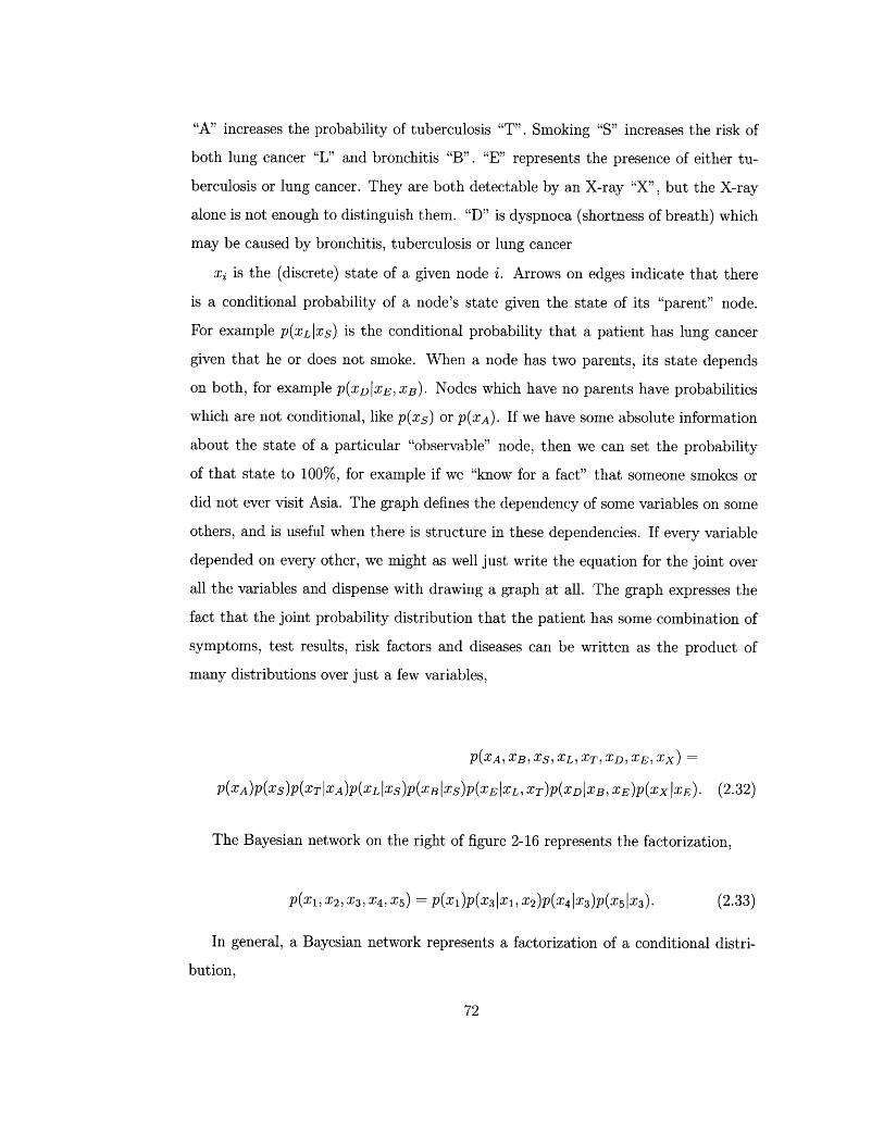
"A" increases the probability of tuberculosis "T". Smoking "S" increases the risk of
both lung cancer "L" and bronchitis "B". "E" represents the presence of either tu-
berculosis or lung cancer. They are both detectable by an X-ray "X", but the X-ray
alone is not enough to distinguish them. "D" is dyspnoea (shortness of breath) which
may be caused by bronchitis, tuberculosis or lung cancer
xi is the (discrete) state of a given node i. Arrows on edges indicate that there
is a conditional probability of a node's state given the state of its "parent" node.
For example p(xLIxs) is the conditional probability that a patient has lung cancer
given that he or does not smoke. When a node has two parents, its state depends
on both, for example p(xD XE, XB). Nodes which have no parents have probabilities
which are not conditional, like p(xs) or p(XA). If we have some absolute information
about the state of a particular "observable" node, then we can set the probability
of that state to 100%, for example if we "know for a fact" that someone smokes or
did not ever visit Asia. The graph defines the dependency of some variables on some
others, and is useful when there is structure in these dependencies. If every variable
depended on every other, we might as well just write the equation for the joint over
all the variables and dispense with drawing a graph at all. The graph expresses the
fact that the joint probability distribution that the patient has some combination of
symptoms, test results, risk factors and diseases can be written as the product of
many distributions over just a few variables,
P(XA, XB, XS, XL, XT, XD, XE, X)
p(XA)p(xs)p(XT XA)P(XL I XS)p(XB IS)p(XE XL,XT)p(XD IXB, XE)p(X XIE). (2.32)
The Bayesian network on the right of figure 2-16 represents the factorization,
p(xi, x2, x 3, x 4, X5 ) = p(Xi)p(x 3 |Xi, x 2)p(X4|x3)p(X5IX 3). (2.33)
In general, a Bayesian network represents a factorization of a conditional distri-
bution,
n
P(Xr,12 ). ... I XN) = rU p(xi 1parents (xi)). (2.34)i=1
2.5.2 Markov Random Fields
An MRF is an undirected graph G, with vertices and edges (V, E). Each vertex V
corresponds to a random variable in the model. Every node has neighbor nodes which
are the nodes to which it is directly connected by an edge. Every variable in an MRF
is independent of all the other variables in the model given its neighbors so that
(Vx E V)p(xIV\{x}) = p(xjn(x)) (2.35)
where n(x) is the set of neighbors of x. An MRF is a graphical representation of
how a global probability distribution over all of the random variables can be "factored"
into a product of several lower dimensional probability distributions. Recall that the
probability of an event A is equal to the product of the events that cause A so long
as the causes are independent from one another; Independent probabilities simply
multiply. An MRF is a pictorial representation of a product of potential functions.
Once we normalize the product of the potential functions we have a joint probability
distribution over all the random variables in the system,
p(X1 , X2 1 .. XN) = 1 flfa (Va) 1 (2.36)Za
where a is an index labelling M functions, fA, fB, fc, . . . , fm, where the func-
tion fa(Xa) has arguments Xa that are some subset of {x1, x 2 , ... ,XN, and Z is a
normalization pre-factor.
An edge connecting two nodes in an MRF represents the fact that those two
random variables are NOT always independent. It turns out that if each function,
fa(V), is identified with a completely inter-connected group of variable nodes known
as a "clique," then it is always possible to draw an MRF graph for any product of
fa(Va)'s. The converse is also true; if we choose non-overlapping cliques to correspond
to fa(Va)'s, then it is always possible to find a product of fa(Va)'s that corresponds to
any MRF that we can draw. This correspondence between a graph and a factorization
of a probability distribution is called the Hammersley-Clifford Theorem.
2.5.3 Factor Graphs
Just like an MRF, the factor graph represents a product of potential functions. Un-
like an MRF, potential functions in a factor graph are not defined over more than
two nodes - so that there are no cliques in a factor graph which contain more than
two nodes. In a factor graph, potential functions over more than two variables are
represented by connecting all of the variables in the potential to a single factor node.
Factor graphs make it easy to identify each potential function with a corresponding
node which is not always immediately obvious in an MRF.
This is especially useful in the context of graphs for representing error correcting
codes (ECC). In error correction coding, it is useful to make a distinction between
variable nodes, which represent measured data from the channel or guesses by the
decoder about symbols sent by the transmitter, and factor nodes which represent
constraint functions (checksum operations or sub-codes). In error correction coding,
the constraint functions act to impose the limitation that there can be no probability
mass over certain values of the domain of the joint distribution. In other words, the
constraint functions zero out the joint probability distribution for certain values of
the state variables. Mathematically, we could have treated variables and constraint
functions alike, as factors in the joint probability distribution represented by the
overall graph, but in practice they play different roles and it is useful to represent
this difference visually.
2.5.4 Forney Factor Graphs (FFG)
In a factor graph, variable nodes store values while factor nodes compute functions
on them and unlike other graphical models, there is a one to one correspondence
between functions and the factor nodes which represent them. This means that we
don't really need to represent the variables explicitly in the graph. The functions are
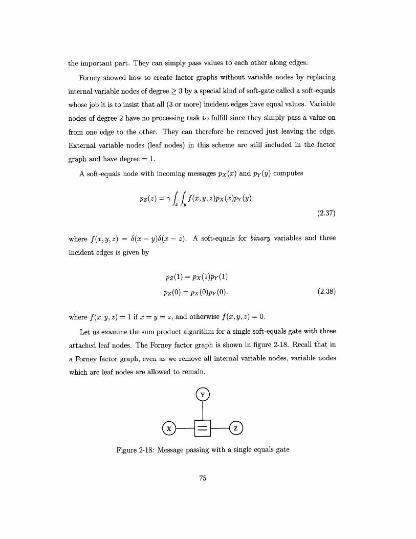
the important part. They can simply pass values to each other along edges.
Forney showed how to create factor graphs without variable nodes by replacing
internal variable nodes of degree > 3 by a special kind of soft-gate called a soft-equals
whose job it is to insist that all (3 or more) incident edges have equal values. Variable
nodes of degree 2 have no processing task to fulfill since they simply pass a value on
from one edge to the other. They can therefore be removed just leaving the edge.
External variable nodes (leaf nodes) in this scheme are still included in the factor
graph and have degree = 1.
A soft-equals node with incoming messages px(x) and py(y) computes
pz(z) = -Y f(x, y, z)px(x)py (y)
(2.37)
where f(x, y, z) = 6(x - y)6(x - z). A soft-equals for binary variables and three
incident edges is given by
pz(1) = px()pY (1)
Pz(0) = px(O)py(0). (2.38)
where f(x, y, z) = 1 if x = y = z, and otherwise f(x, y, z) = 0.
Let us examine the sum product algorithm for a single soft-equals gate with three
attached leaf nodes. The Forney factor graph is shown in figure 2-18. Recall that in
a Forney factor graph, even as we remove all internal variable nodes, variable nodes
which are leaf nodes are allowed to remain.
0X - z
Figure 2-18: Message passing with a single equals gate
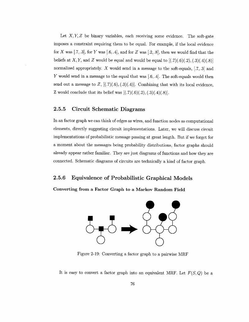
Let X, Y, Z be binary variables, each receiving some evidence. The soft-gate
imposes a constraint requiring them to be equal. For example, if the local evidence
for X was [.7, .3], for Y was [.6, .4], and for Z was [.2, .8], then we would find that the
beliefs at X, Y, and Z would be equal and would be equal to [(.7)(.6)(.2), (.3)(.4)(.8)]
normalized appropriately. X would send in a message to the soft-equals, [.7, .3] and
Y would send in a message to the equal that was [.6, .4]. The soft-equals would then
send out a message to Z, [(.7)(.6), (.3)(.4)]. Combining that with its local evidence,
Z would conclude that its belief was [(.7)(.6)(.2), (.3)(.4)(.8)].
2.5.5 Circuit Schematic Diagrams
In an factor graph we can think of edges as wires, and function nodes as computational
elements, directly suggesting circuit implementations. Later, we will discuss circuit
implementations of probabilistic message passing at great length. But if we forget for
a moment about the messages being probability distributions, factor graphs should
already appear rather familiar. They are just diagrams of functions and how they are
connected. Schematic diagrams of circuits are technically a kind of factor graph.
2.5.6 Equivalence of Probabilistic Graphical Models
Converting from a Factor Graph to a Markov Random Field
Figure 2-19: Converting a factor graph to a pairwise MRF
It is easy to convert a factor graph into an equivalent MRF. Let F(S, Q) be a
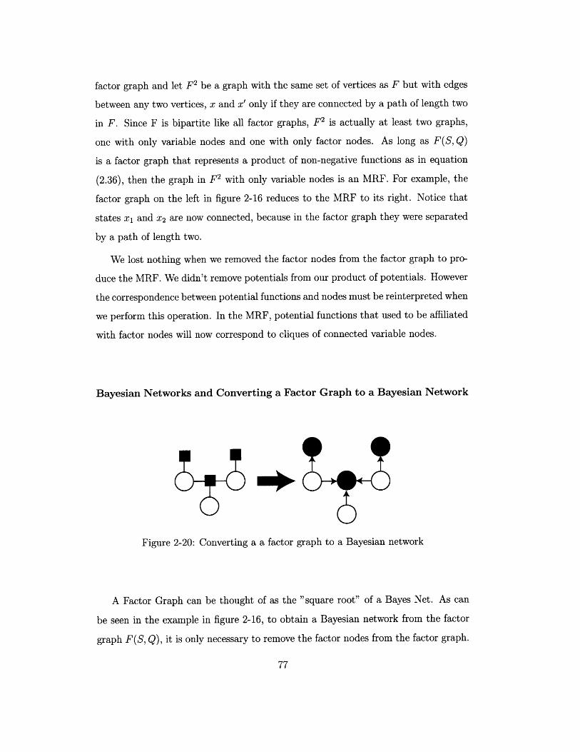
factor graph and let F2 be a graph with the same set of vertices as F but with edges
between any two vertices, x and x' only if they are connected by a path of length two
in F. Since F is bipartite like all factor graphs, F2 is actually at least two graphs,
one with only variable nodes and one with only factor nodes. As long as F(S, Q)is a factor graph that represents a product of non-negative functions as in equation
(2.36), then the graph in F 2 with only variable nodes is an MRF. For example, the
factor graph on the left in figure 2-16 reduces to the MRF to its right. Notice that
states xi and X2 are now connected, because in the factor graph they were separated
by a path of length two.
We lost nothing when we removed the factor nodes from the factor graph to pro-
duce the MRF. We didn't remove potentials from our product of potentials. However
the correspondence between potential functions and nodes must be reinterpreted when
we perform this operation. In the MRF, potential functions that used to be affiliated
with factor nodes will now correspond to cliques of connected variable nodes.
Bayesian Networks and Converting a Factor Graph to a Bayesian Network
Figure 2-20: Converting a a factor graph to a Bayesian network
A Factor Graph can be thought of as the "square root" of a Bayes Net. As can
be seen in the example in figure 2-16, to obtain a Bayesian network from the factor
graph F(S, Q), it is only necessary to remove the factor nodes from the factor graph.
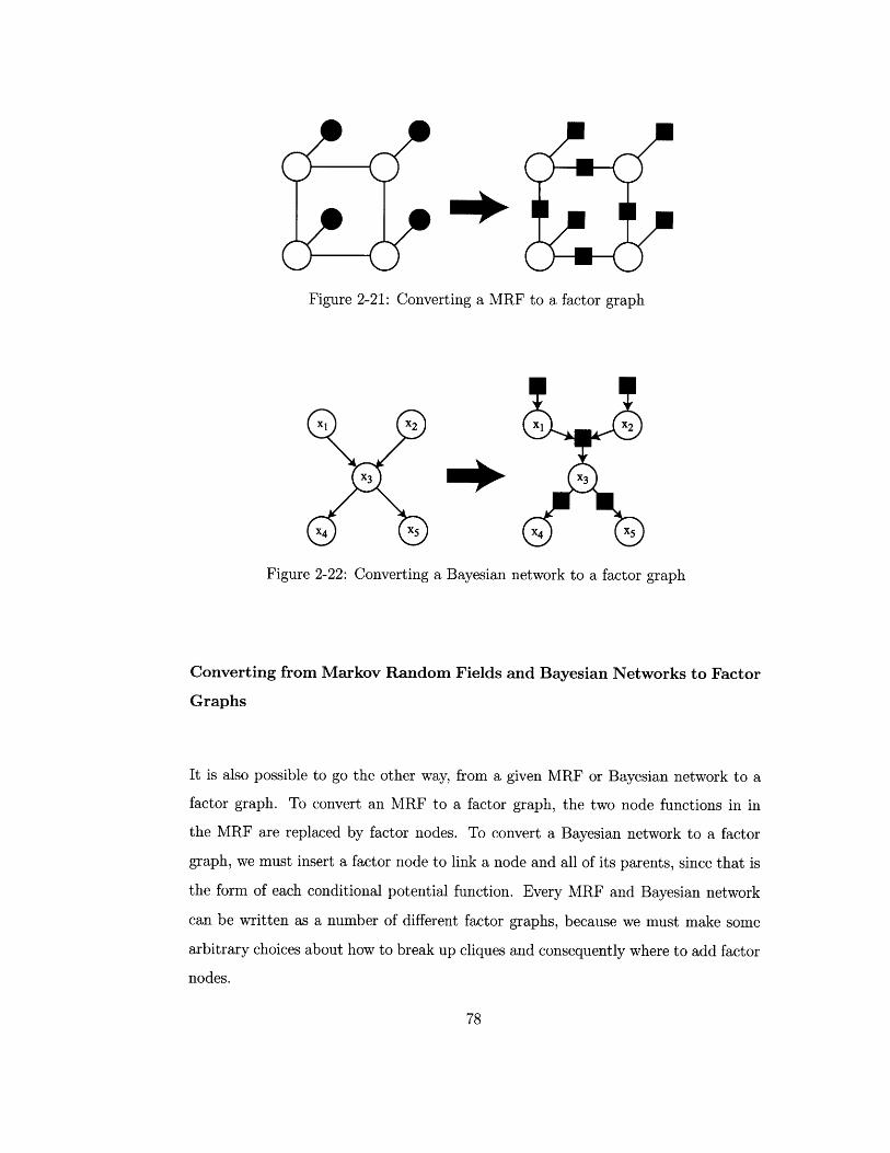
Figure 2-21: Converting a MRF to a factor graph
X1 X2 X1 X2
X3 MO .X3
X4 X5 X4 X5
Figure 2-22: Converting a Bayesian network to a factor graph
Converting from Markov Random Fields and Bayesian Networks to Factor
Graphs
It is also possible to go the other way, from a given MRF or Bayesian network to a
factor graph. To convert an MRF to a factor graph, the two node functions in in
the MRF are replaced by factor nodes. To convert a Bayesian network to a factor
graph, we must insert a factor node to link a node and all of its parents, since that is
the form of each conditional potential function. Every MRF and Bayesian network
can be written as a number of different factor graphs, because we must make some
arbitrary choices about how to break up cliques and consequently where to add factor
nodes.
2.6 Representations of Messages: Likelihood Ra-
tio and Log-likelihood Ratio
2.6.1 Log-Likelihood Formulation of the Soft-Equals
The definition of the log-likelihood ratio (log-likelihood) is
Lz = In Pz(0) . (2.39)
In the log-likelihood representation, the product message from an soft-equals gate can
be written as
Lz = Lx + Ly. (2.40)
To see this, we begin by manipulating the definition of the log-likelihood,
Lz = In [pz(0)] (2.41)[pz(1).1
= ln I (2.42)1px(1)pay(1)
= Lx + Ly. (2.43)
2.6.2 Log-Likelihood Formulation of the Soft-xor
In the log-likelihood representation, the product message from an soft-xor gate can
be written as
tanh(Lz/2) = tanh(Lx/2) tanh(Ly/2). (2.44)
To see this, we begin by manipulating the definition of the log-likelihood,
Lz = ln pz(0) (2.45)
= n x (0)pmy (0)+ ptx(1)Ipy(1) (2.46)1 Ax(1) py (0) + px (0)py( 1)
-lx(0) y (0)
= In E "() ± M + (2.47)Ax (0) + tty(0). x(1) py(1) .
In exp(Lx + Ly) + 1 (2.48).exp (Lx) + exp (Ly)
exp(Lz) = exp(Lx + Ly) +11 (2.49).exp(Lx) + exp(Ly).*
Multiplying both sides by the denominator of the right side we obtain
exp(Lx + Ly) = exp(Lx + Lz) + exp(Ly + Lz) - 1. (2.50)
As can be seen by multiplying by the denominators of both sides of the following
expression, the last equation is a simplification of the following
exp(Lx + Ly) - exp(Lx) - exp(Ly) + 1exp(Lx + Ly) + exp(Lx) + exp(Ly) + 1
The left hand side of this equation can be factored into
(exp(Lx) - 1)(exp(Ly) - 1)
(exp(Lx) + 1)(exp(Ly) + 1)exp(Lz) - 1exp(Lz) + 1
remembering the definition of tanh
ex e-Xtanh(x) = ex A-x
exp(2x) - 1
exp(2x) + 1 (2.53)
we can finally write the message from soft-xor in terms of log-likelihoods as
tanh(Lz/2) = tanh(Lx/2) tanh(Ly/2).
exp(Lz) - 1exp(Lz) + I
(2.51)
(2.52)
(2.54)
2.7 Derivation of Belief Propagation from Varia-
tional Methods
In the previous sections we derived the sum product algorithm by observing that
marginalization could be simplified by performing local marginalization at each fac-
tor node and passing on the answer. Another way to understand message passing
algorithms involves the calculus of variations. The sum product algorithm can be
understood as minimizing a "free energy" function with Lagrangian constraints. In
this scheme, each factor node is thought of as imposing a constraint on the shape of
the joint distribution and therefore also constrains the marginal distribution that we
are attempting to find. This is easier to understand in the context of an example and
is presented in the next chapter in the example on routing in an adhoc peer-to-peer
networks.

-- erere. - - - - - .au --
Chapter 3
Examples of Probabilistic Message
Passing on Graphs
3.1 Kalman Filter
In this example we explore a practical example of a the sum product algo-
rithm on graphs with a one-dimensional "chain" topology. The operations are
on probability distributions of continuous-valued variables. Message passing
occurs in only one direction (forward) on the graph.
We use a Kalman filter when we have a good model for the update dynamics of a
system but we cannot directly observe the (hidden) internal state of the system. Since
we cannot directly observe the internal state of the system, we measure something
about the system which we know is related to the internal state. Then, using succes-
sive measurements, we repeatedly update the state of our model of the system until it
(hopefully) corresponds to the hidden internal state of the system we are observing.
The canonical example is the task of continuously estimating the position of an
airplane. The airplane has a current state, zt given by its position, velocity and
acceleration in three-space as well as the positions of its control surfaces. The state
is updated in discrete-time according to a distribution function pVst+1zIet), which
includes both deterministic influences (aerodynamics) and random influences (turbu-
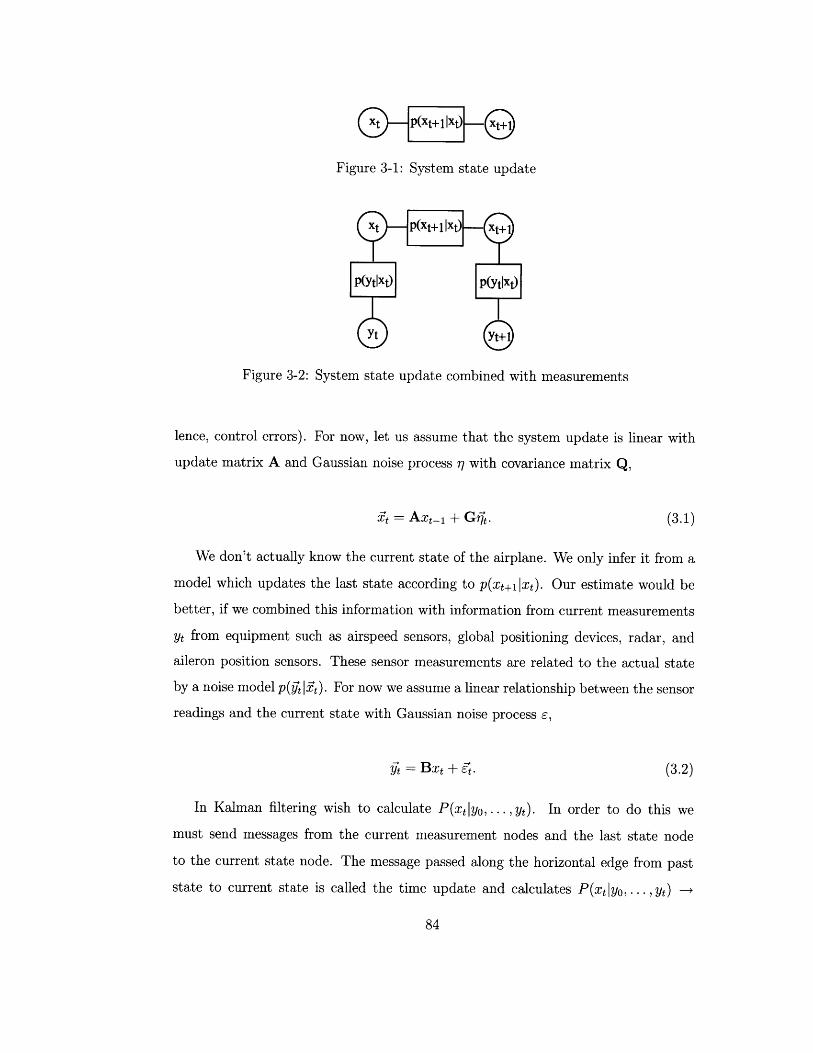
t P(Xt+1| X0-
Figure 3-1: System state update
(Xt dP(Xt+Xo Xt+
P(7|X Pxyt|Xo
Yt
Figure 3-2: System state update combined with measurements
lence, control errors). For now, let us assume that the system update is linear with
update matrix A and Gaussian noise process r/ with covariance matrix Q,
-= Ax- 1 + Git. (3.1)
We don't actually know the current state of the airplane. We only infer it from a
model which updates the last state according to p(xti Ixt). Our estimate would be
better, if we combined this information with information from current measurements
yt from equipment such as airspeed sensors, global positioning devices, radar, and
aileron position sensors. These sensor measurements are related to the actual state
by a noise model p(g lse). For now we assume a linear relationship between the sensor
readings and the current state with Gaussian noise process E,
t = Bxt + t. (3.2)
In Kalman filtering wish to calculate P(xtlyo,..., yt). In order to do this we
must send messages from the current measurement nodes and the last state node
to the current state node. The message passed along the horizontal edge from past
state to current state is called the time update and calculates P(xtlyo,..., yt) -+
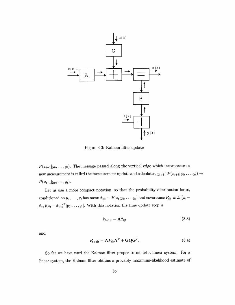
u[k]
x[k-1 x[k]
E[k]
ty [k]
Figure 3-3: Kalman filter update
P(xt+1 Iyo, ... , yt). The message passed along the vertical edge which incorporates a
new measurement is called the measurement update and calculates, yt+i: P(xt+1|yo, ... , Yt)
P(xt+iIyo, ..., yt).
Let us use a more compact notation, so that the probability distribution for xt
conditioned on yo, . .. , yt has mean:stit = E[xt Iyo, . . . , yt] and covariance Ptit = E[(xt-
ftlt)(xt - stit)Tjyo, .. -, Yt]. With this notation the time update step is
setii, = Assit (3.3)
and
Pt+ 11t = AP tA T + GQGT. (3.4)
So far we have used the Kalman filter proper to model a linear system. For a
linear system, the Kalman filter obtains a provably maximum-likelihood estimate of
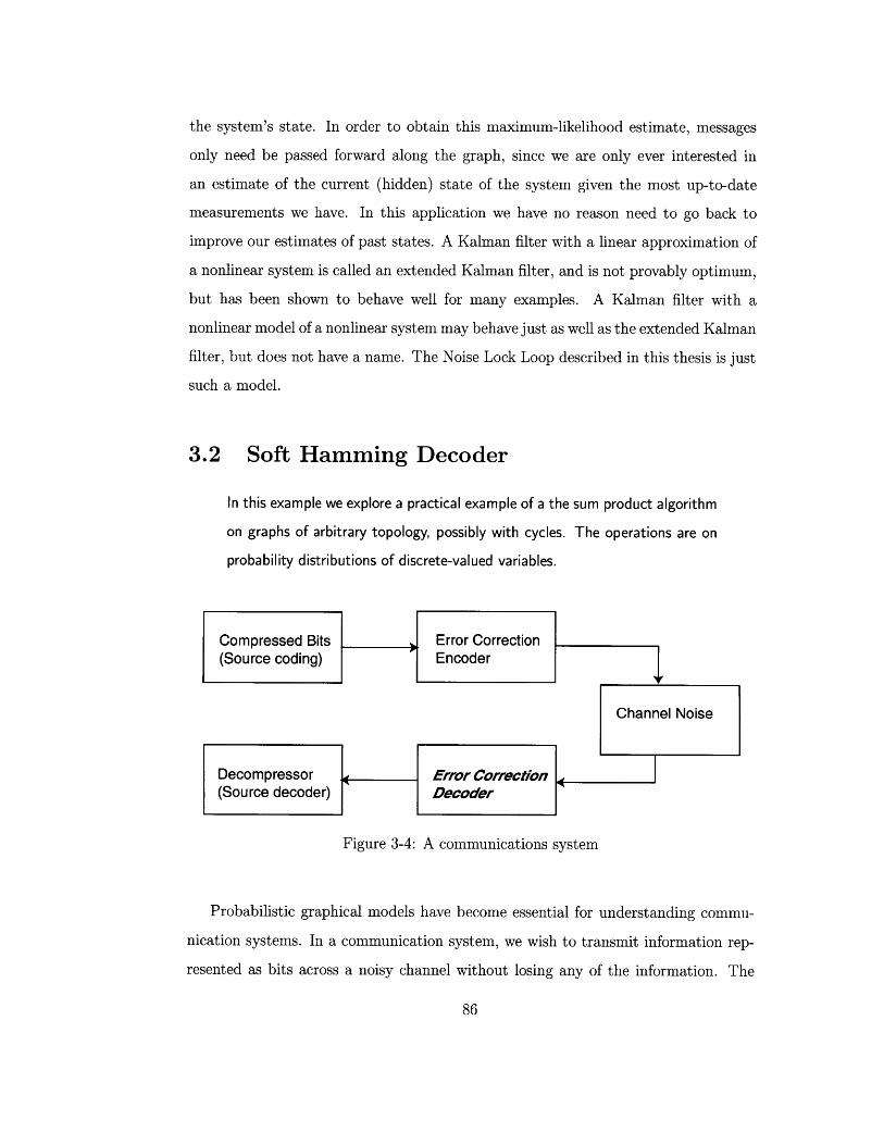
the system's state. In order to obtain this maximum-likelihood estimate, messages
only need be passed forward along the graph, since we are only ever interested in
an estimate of the current (hidden) state of the system given the most up-to-date
measurements we have. In this application we have no reason need to go back to
improve our estimates of past states. A Kalman filter with a linear approximation of
a nonlinear system is called an extended Kalman filter, and is not provably optimum,
but has been shown to behave well for many examples. A Kalman filter with a
nonlinear model of a nonlinear system may behave just as well as the extended Kalman
filter, but does not have a name. The Noise Lock Loop described in this thesis is just
such a model.
3.2 Soft Hamming Decoder
In this example we explore a practical example of a the sum product algorithm
on graphs of arbitrary topology, possibly with cycles. The operations are on
probability distributions of discrete-valued variables.
Compressed Bits Error Correction
(Source coding) Encoder
Channel Noise
De compressor Error C11orrect/on g(Source decoder) Decoder
Figure 3-4: A communications system
Probabilistic graphical models have become essential for understanding commu-
nication systems. In a communication system, we wish to transmit information rep-
resented as bits across a noisy channel without losing any of the information. The
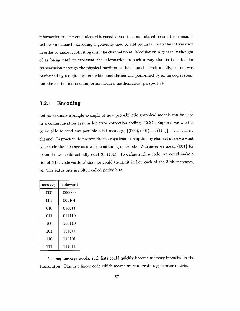
information to be communicated is encoded and then modulated before it is transmit-
ted over a channel. Encoding is generally used to add redundancy to the information
in order to make it robust against the channel noise. Modulation is generally thought
of as being used to represent the information in such a way that is is suited for
transmission through the physical medium of the channel. Traditionally, coding was
performed by a digital system while modulation was performed by an analog system,
but the distinction is unimportant from a mathematical perspective.
3.2.1 Encoding
Let us examine a simple example of how probabilistic graphical models can be used
in a communication system for error correction coding (ECC). Suppose we wanted
to be able to send any possible 3 bit message, {(000), (001),.. . (111)}, over a noisy
channel. In practice, to protect the message from corruption by channel noise we want
to encode the message as a word containing more bits. Whenever we mean {001} for
example, we could actually send (001101). To define such a code, we could make a
list of 6-bit codewords, x that we could transmit in lieu each of the 3-bit messages,
ni. The extra bits are often called parity bits.
message codeword
000 000000
001 001101
010 010011
011 011110
100 100110
101 101011
110 110101
111 111011
For long message words, such lists could quickly become memory intensive in the
transmitter. This is a linear code which means we can create a generator matrix,
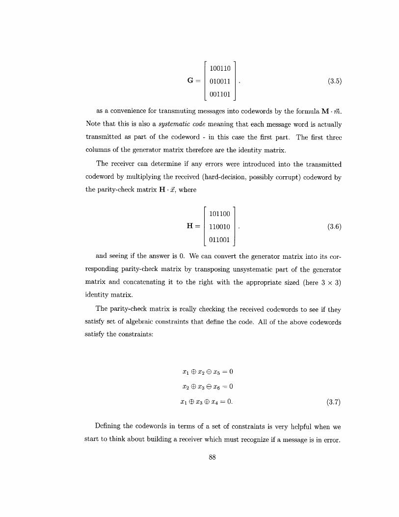
100110
G = 010011 . (3.5)
001101
as a convenience for transmuting messages into codewords by the formula M - i.
Note that this is also a systematic code meaning that each message word is actually
transmitted as part of the codeword - in this case the first part. The first three
columns of the generator matrix therefore are the identity matrix.
The receiver can determine if any errors were introduced into the transmitted
codeword by multiplying the received (hard-decision, possibly corrupt) codeword by
the parity-check matrix H -x, where
101100
H 110010 (3.6)
011001
and seeing if the answer is 0. We can convert the generator matrix into its cor-
responding parity-check matrix by transposing unsystematic part of the generator
matrix and concatenating it to the right with the appropriate sized (here 3 x 3)
identity matrix.
The parity-check matrix is really checking the received codewords to see if they
satisfy set of algebraic constraints that define the code. All of the above codewords
satisfy the constraints:
X1 E x2 e x5 = 0
x 2 E X3 (Dx6 = 0
X1 E x 3 e x4 = 0. (3.7)
Defining the codewords in terms of a set of constraints is very helpful when we
start to think about building a receiver which must recognize if a message is in error.
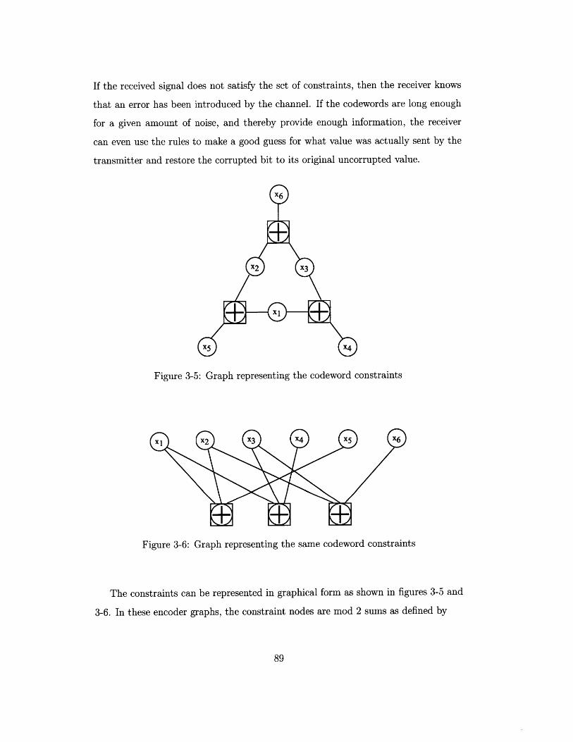
If the received signal does not satisfy the set of constraints, then the receiver knows
that an error has been introduced by the channel. If the codewords are long enough
for a given amount of noise, and thereby provide enough information, the receiver
can even use the rules to make a good guess for what value was actually sent by the
transmitter and restore the corrupted bit to its original uncorrupted value.
Figure 3-5: Graph representing the codeword constraints
Figure 3-6: Graph representing the same codeword constraints
The constraints can be represented in graphical form as shown in figures 3-5 and
3-6. In these encoder graphs, the constraint nodes are mod 2 sums as defined by
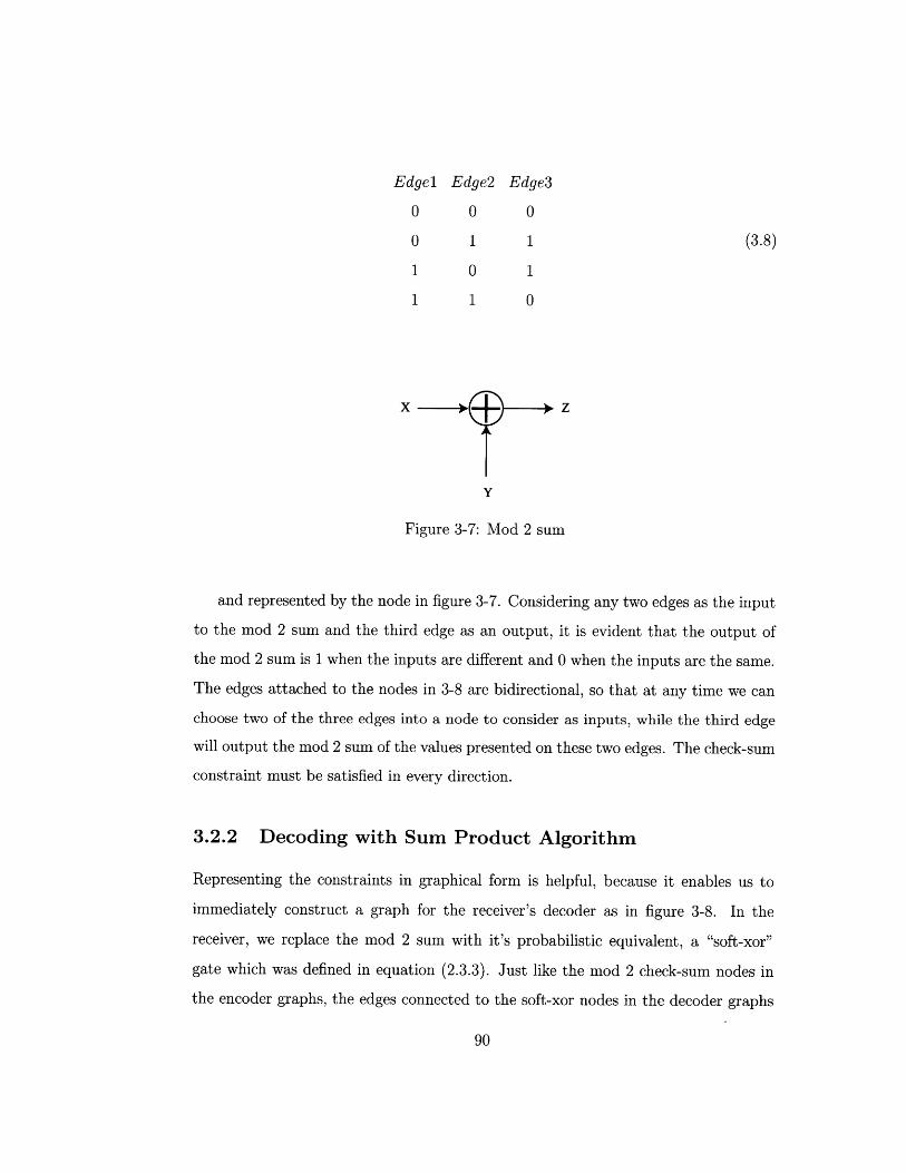
Edge1 Edge2 Edge3
0 0 0
0 1 1 (3.8)
1 0 1
1 1 0
X YA z
Y
Figure 3-7: Mod 2 sum
and represented by the node in figure 3-7. Considering any two edges as the input
to the mod 2 sum and the third edge as an output, it is evident that the output of
the mod 2 sum is 1 when the inputs are different and 0 when the inputs are the same.
The edges attached to the nodes in 3-8 are bidirectional, so that at any time we can
choose two of the three edges into a node to consider as inputs, while the third edge
will output the mod 2 sum of the values presented on these two edges. The check-sum
constraint must be satisfied in every direction.
3.2.2 Decoding with Sum Product Algorithm
Representing the constraints in graphical form is helpful, because it enables us to
immediately construct a graph for the receiver's decoder as in figure 3-8. In the
receiver, we replace the mod 2 sum with it's probabilistic equivalent, a "soft-xor"
gate which was defined in equation (2.3.3). Just like the mod 2 check-sum nodes in
the encoder graphs, the edges connected to the soft-xor nodes in the decoder graphs
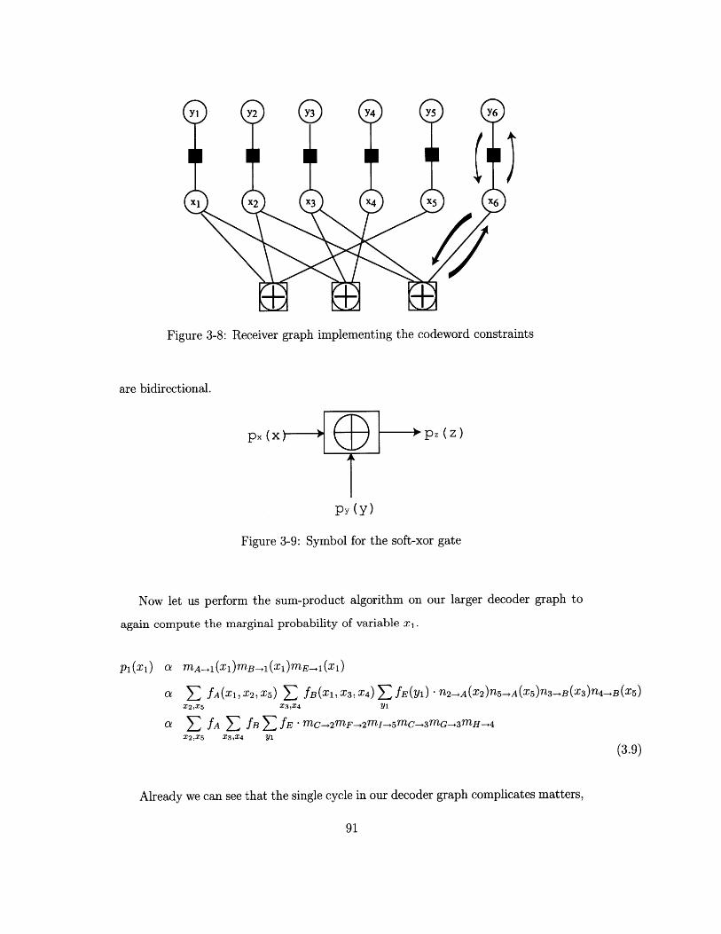
Figure 3-8: Receiver graph implementing the codeword constraints
are bidirectional.
px (x Pz (z)
py (y)
Figure 3-9: Symbol for the soft-xor gate
Now let us perform the sum-product algorithm on our larger decoder graph to
again compute the marginal probability of variable x1 .
P1(X 1) a MA-1(1)mB-1(x1)mEE-+1(X 1 )
a S: fA(X1, X2, X5) S fB(X1, X3 , X4) T fE(Y1) '2-A (X2)5-A (X5)n3-+.*B(X3)n4->B(X5)X2,X5 X3,X4 Y1
a S fA E fBX2,X5 X3,X4
E fE *MC,2mF-2mI-5mC->3mG->3mH-+4Y1
(3.9)
Already we can see that the single cycle in our decoder graph complicates matters,
A* I-
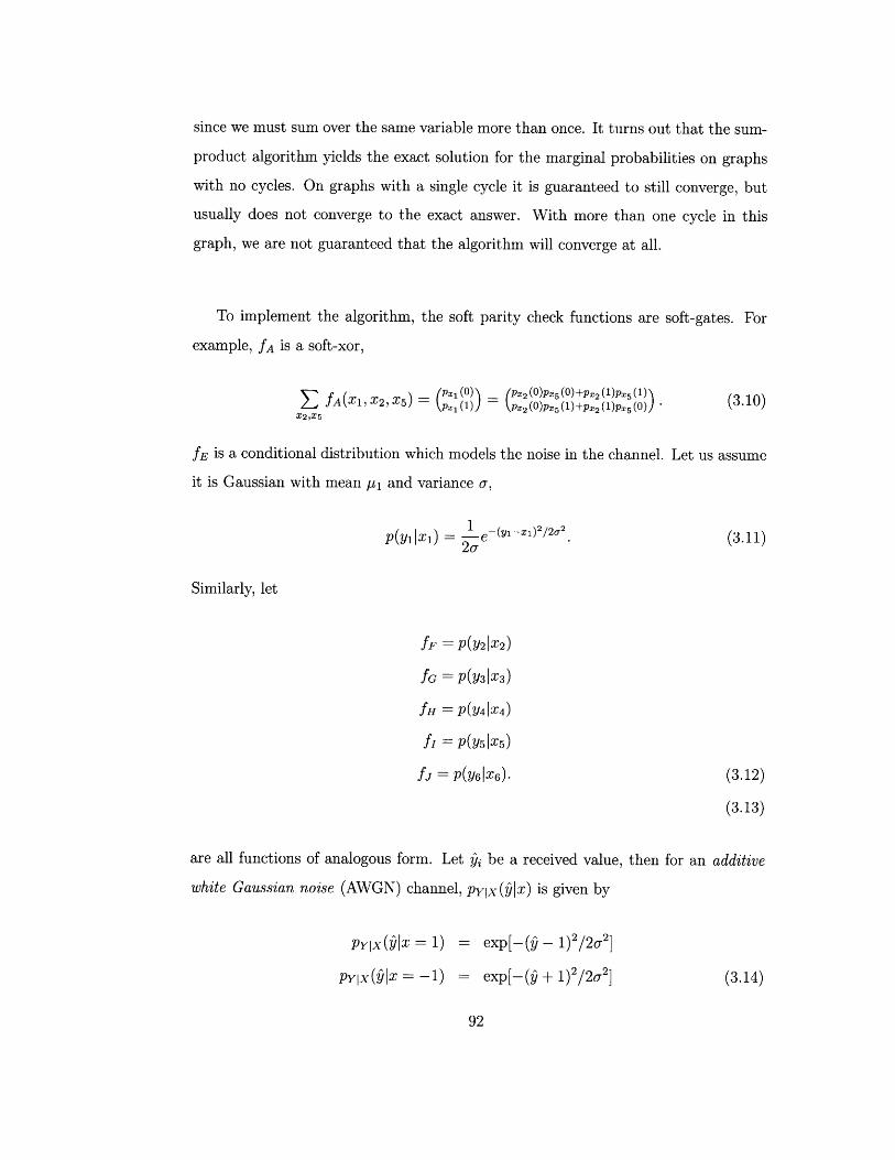
since we must sum over the same variable more than once. It turns out that the sum-
product algorithm yields the exact solution for the marginal probabilities on graphs
with no cycles. On graphs with a single cycle it is guaranteed to still converge, but
usually does not converge to the exact answer. With more than one cycle in this
graph, we are not guaranteed that the algorithm will converge at all.
To implement the algorithm, the soft parity check functions are soft-gates. For
example, fA is a soft-xor,
SfA (X1,X2),X5) =(P., (0) ( P-2(O)PX5 ()+PX2 (1)P'5 (1)) (3.10)X2,X5
fE is a conditional distribution which models the noise in the channel. Let us assume
it is Gaussian with mean p1 and variance o-,
p(y1|1X1) = I - (y1-X1)2/20,2.(1)
Similarly, let
fF =P(y2 X2)
fG = P(Y3X3)
fH =P(Y94 X4)
h=Py 5 X5)
bi = P(y6 x6). (3.12)
(3.13)
are all functions of analogous form. Let Qj be a received value, then for an additive
white Gaussian noise (AWGN) channel, pyx(Ilx) is given by
PY|X(Ix = 1) = exp[-( - 1)2 /20 2
PY|X(Q= -1) = exp[-( 1)2/2U2 ] (3.14)
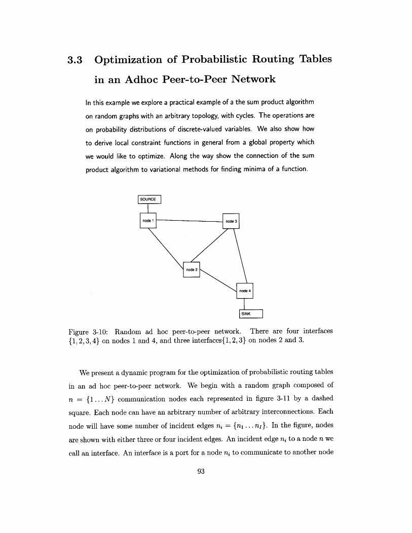
3.3 Optimization of Probabilistic Routing Tables
in an Adhoc Peer-to-Peer Network
In this example we explore a practical example of a the sum product algorithm
on random graphs with an arbitrary topology, with cycles. The operations are
on probability distributions of discrete-valued variables. We also show how
to derive local constraint functions in general from a global property which
we would like to optimize. Along the way show the connection of the sum
product algorithm to variational methods for finding minima of a function.
SOURCE
node 1 -node 3
node 2
node 4
|SINK
Figure 3-10: Random ad hoc peer-to-peer network. There are four interfaces{1, 2, 3, 4} on nodes 1 and 4, and three interfaces{1, 2, 3} on nodes 2 and 3.
We present a dynamic program for the optimization of probabilistic routing tables
in an ad hoc peer-to-peer network. We begin with a random graph composed of
n = {1 ... N} communication nodes each represented in figure 3-11 by a dashed
square. Each node can have an arbitrary number of arbitrary interconnections. Each
node will have some number of incident edges ni = {n1 ... nr}. In the figure, nodes
are shown with either three or four incident edges. An incident edge ni to a node n we
call an interface. An interface is a port for a node ni to communicate to another node
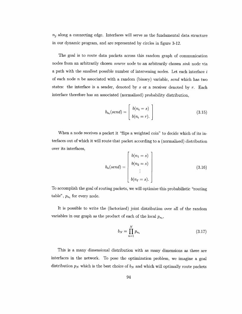
n3 along a connecting edge. Interfaces will serve as the fundamental data structure
in our dynamic program, and are represented by circles in figure 3-12.
The goal is to route data packets across this random graph of communication
nodes from an arbitrarily chosen source node to an arbitrarily chosen sink node via
a path with the smallest possible number of intervening nodes. Let each interface i
of each node n be associated with a random (binary) variable, send which has two
states: the interface is a sender, denoted by s or a receiver denoted by r. Each
interface therefore has an associated (normalized) probability distribution,
[b(ni = s)1bni (send) =~ i s (3.15)
b(ni =r).
When a node receives a packet it "flips a weighted coin" to decide which of its in-
terfaces out of which it will route that packet according to a (normalized) distribution
over its interfaces,
b(ni = s)
bn(send) b(n2 s) (3.16)
b(ni s).
To accomplish the goal of routing packets, we will optimize this probabilistic "routing
table", pni for every node.
It is possible to write the (factorized) joint distribution over all of the random
variables in our graph as the product of each of the local pn,
N
bN = pni (3.17)n=1
This is a many dimensional distribution with as many dimensions as there are
interfaces in the network. To pose the optimization problem, we imagine a goal
distribution PN which is the best choice of bN and which will optimally route packets
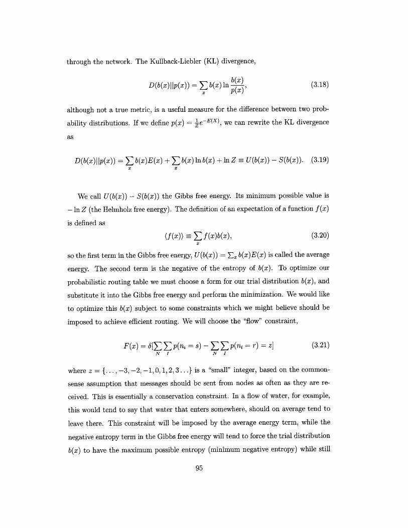
through the network. The Kullback-Liebler (KL) divergence,
D(b(x)Ip(x)) = b(x) In b(x) (3.18)p(x)
although not a true metric, is a useful measure for the difference between two prob-
ability distributions. If we define p(x) = e-E(X), we can rewrite the KL divergence
as
D(b(x)I|p(x)) = Zb(x)E(x) + b(x)lnb(x) +IlnZ =U(b(x)) - S(b(x)). (3.19)X x
We call U(b(x)) - S(b(x)) the Gibbs free energy. Its minimum possible value is
- In Z (the Helmholz free energy). The definition of an expectation of a function f(x)
is defined as
(f(x)) Zf(x)b(x), (3.20)
so the first term in the Gibbs free energy, U(b(x)) = E b(x)E(x) is called the average
energy. The second term is the negative of the entropy of b(x). To optimize our
probabilistic routing table we must choose a form for our trial distribution b(x), and
substitute it into the Gibbs free energy and perform the minimization. We would like
to optimize this b(x) subject to some constraints which we might believe should be
imposed to achieve efficient routing. We will choose the "flow" constraint,
F(x) = 6[E E p(ni = s) - > Z p(ni = r) = z] (3.21)N I N I
where z = {. .. ,-3, -2, -1, 0,1, 2, 3.. .} is a "small" integer, based on the common-
sense assumption that messages should be sent from nodes as often as they are re-
ceived. This is essentially a conservation constraint. In a flow of water, for example,
this would tend to say that water that enters somewhere, should on average tend to
leave there. This constraint will be imposed by the average energy term, while the
negative entropy term in the Gibbs free energy will tend to force the trial distribution
b(x) to have the maximum possible entropy (minimum negative entropy) while still
satisfying the constraint. Since the uniform distribution is the maximum entropy
distribution, this will tend to spread probability over all of p(x) as much as possible
subject to the flow constraint, thereby tending to distribute satisfaction of the flow
constraint across the network. We will impose the global flow constraint f(x), by
choosing an energy function of the form,
E(x) = exp [ln f(x)] . (3.22)
Optimizing this many-dimensional distribution would be computationally pro-
hibitive. However, we can factorize the global flow constraint function into many
local constraints in order to make the computation more tractable. This will require
that we make some assumptions about which variables must be modelled as being
directly dependent on one another. Once we decide what dependencies between vari-
ables are important to model, the dependencies can be conveniently represented in
graphical form by a factor graph.
For example, we will begin by hoping that stable routing can be achieved with
only nearest-neighbor connections. This means that we can derive the factor graph
of dependencies graph from the ad hoc network itself as shown in figure 3-12. Other
dependencies could also exist, but are a subject for future work.
Constraint functions in figure 3-12 are indicated by black squares. We will actually
use two constraint functions, one between two interfaces connecting different nodes
f(bi, bj), and one between the multiple interfaces of a single node g(bk, bl, bin, b, . . .).
If two interfaces i and j from two different nodes are connected, this represents a
path for packets to flow from node to node, so it makes sense that if one interface is
the sender the other ought to be a receiver. This condition can be enforced by the
constraint
f(x) 6 (pi(s) - pj (r) = 0)6(pj (s) - pi (r) = 0). (3.23)
If multiple interfaces {k, 1, m} belong to the same node, it makes sense that at least
one should be a receiver and at least one should be a transmitter which can be enforced
by the constraint
Figure 3-11: Factor graph derived from ad hoc peer-to-peer network.
g(x) = 6(pk(s) + p(s) + Pm(S) - pk(r) - pl(r) - pm(r) = 1)'
5(pk(s)+ p(s)+ p m(S) - Pk(r) - p,(r) - pm(r) = 2). (3.24)
We can use the sum-product algorithm to minimize the Gibbs free energy under
these constraints. In order to do this we must derive probabilistic messages to pass
from function nodes f in our factor graph to interface nodes, from function nodes g to
interface nodes, and from interface nodes to function nodes. Messages from function
nodes f, connected to two interfaces are denoted by
p(i) = Epj(j)f(i, j). (3.25)
3
With the constraint that a sender sends to a receiver, the function between two
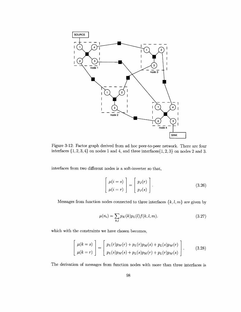
- 14Dnode 2
Figure 3-12: Factor graph derived from adinterfaces {1, 2, 3, 4} on nodes 1 and 4, and
hoc peer-to-peer network. There are fourthree interfaces{1, 2, 3} on nodes 2 and 3.
interfaces from two different nodes is a soft-inverter so that,
p(i =S)p r )
pj(r)
pj(s)(3.26)
Messages from function nodes connected to three interfaces {k, 1, m} are given by
p Z(ni) = pK (k)PL () f(k,1,mk,l
which with the constraints we have chosen becomes,
pL(r)pM (r) -- PL (r)pM (s)
pL(S)pM(S) + PL (S)PM (r)
+ PL(s)pM(r)
+ PL(T)pM (S)
The derivation of messages from function nodes with more than three interfaces is
(3.27)
p(k = s)
p(k =)(3.28)
12
3
left as an exercise for the reader. The outgoing message from an interface with two
incident edges is just a copy of the incoming message,
E =(i s) PJ(s)(3.29)
P(i=r) Pi (r)
In addition, we must also impose a normalization constraint on all messages so that
p(i=s)+ p(i =r) = 1 and v(i =s)+ v(i = r) = 1.
Implementation of continuous-time message passing involves an asynchronous
discrete-time approximation. We use a message passing schedule in which a node
sends a message along an incident edge if and only if there are incoming messages
pending on every other incident edge. We will further discuss scheduling in a later
chapter.

100
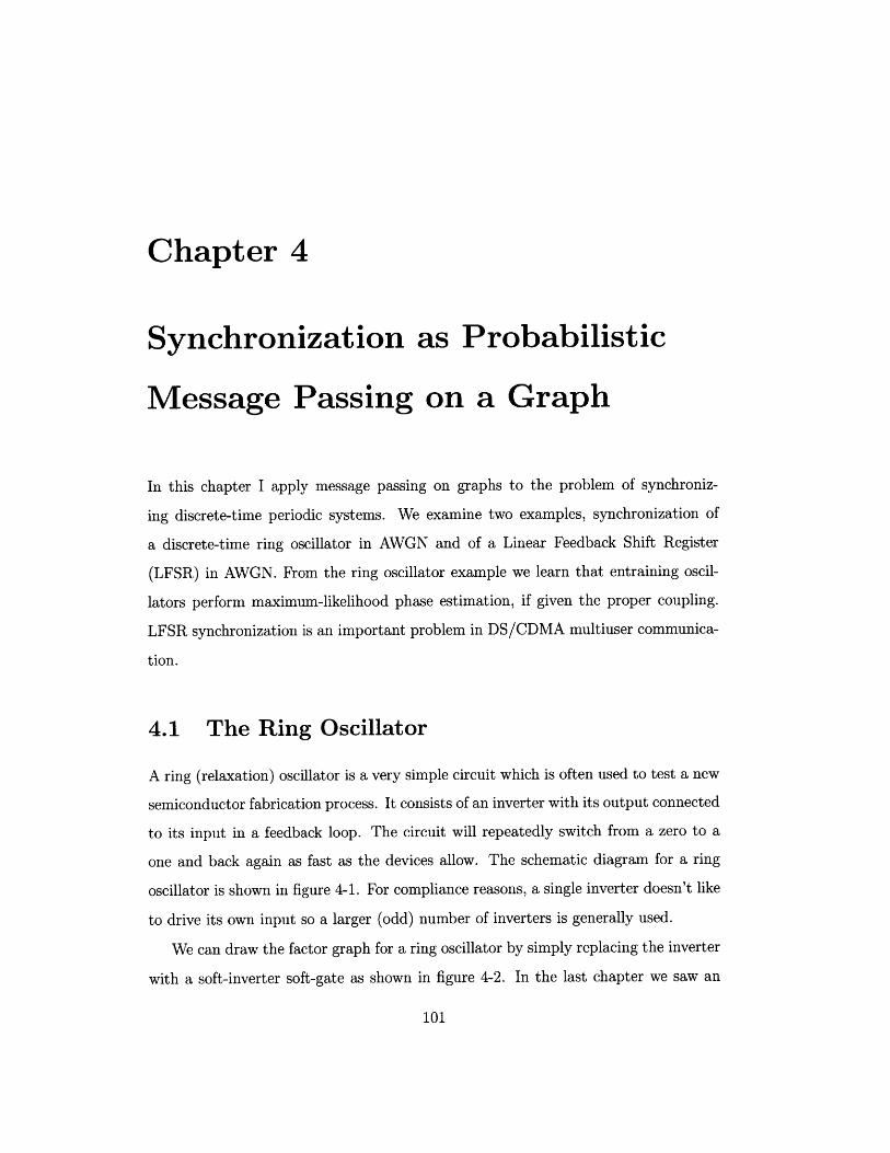
Chapter 4
Synchronization as Probabilistic
Message Passing on a Graph
In this chapter I apply message passing on graphs to the problem of synchroniz-
ing discrete-time periodic systems. We examine two examples, synchronization of
a discrete-time ring oscillator in AWGN and of a Linear Feedback Shift Register
(LFSR) in AWGN. From the ring oscillator example we learn that entraining oscil-
lators perform maximum-likelihood phase estimation, if given the proper coupling.
LFSR synchronization is an important problem in DS/CDMA multiuser communica-
tion.
4.1 The Ring Oscillator
A ring (relaxation) oscillator is a very simple circuit which is often used to test a new
semiconductor fabrication process. It consists of an inverter with its output connected
to its input in a feedback loop. The circuit will repeatedly switch from a zero to a
one and back again as fast as the devices allow. The schematic diagram for a ring
oscillator is shown in figure 4-1. For compliance reasons, a single inverter doesn't like
to drive its own input so a larger (odd) number of inverters is generally used.
We can draw the factor graph for a ring oscillator by simply replacing the inverter
with a soft-inverter soft-gate as shown in figure 4-2. In the last chapter we saw an
101
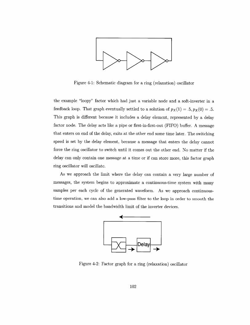
Figure 4-1: Schematic diagram for a ring (relaxation) oscillator
the example "loopy" factor which had just a variable node and a soft-inverter in a
feedback loop. That graph eventually settled to a solution of px(1) = .5,px(O) = .5.
This graph is different because it includes a delay element, represented by a delay
factor node. The delay acts like a pipe or first-in-first-out (FIFO) buffer. A message
that enters on end of the delay, exits at the other end some time later. The switching
speed is set by the delay element, because a message that enters the delay cannot
force the ring oscillator to switch until it comes out the other end. No matter if the
delay can only contain one message at a time or if can store more, this factor graph
ring oscillator will oscillate.
As we approach the limit where the delay can contain a very large number of
messages, the system begins to approximate a continuous-time system with many
samples per each cycle of the generated waveform. As we approach continuous-
time operation, we can also add a low-pass filter to the loop in order to smooth the
transitions and model the bandwidth limit of the inverter devices.
Delay-
Figure 4-2: Factor graph for a ring (relaxation) oscillator
102
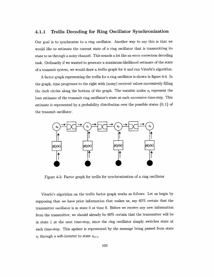
4.1.1 Trellis Decoding for Ring Oscillator Synchronization
Our goal is to synchronize to a ring oscillator. Another way to say this is that we
would like to estimate the current state of a ring oscillator that is transmitting its
state to us through a noisy channel. This sounds a lot like an error correction decoding
task. Ordinarily if we wanted to generate a maximum-likelihood estimate of the state
of a transmit system, we would draw a trellis graph for it and run Viterbi's algorithm.
A factor graph representing the trellis for a ring oscillator is shown in figure 4-4. In
the graph, time progresses to the right with (noisy) received values successively filling
the dark circles along the bottom of the graph. The variable nodes st represent the
best estimate of the transmit ring oscillator's state at each successive time-step. This
estimate is represented by a probability distribution over the possible states {0, 1} of
the transmit oscillator.
SoSIS2 S3
p(ylx) p(ylx) P(yIX) P(yjX)
Figure 4-3: Factor graph for trellis for synchronization of a ring oscillator
Viterbi's algorithm on the trellis factor graph works as follows. Let us begin by
supposing that we have prior information that makes us, say 60% certain that the
transmitter oscillator is in state 0 at time 0. Before we receive any new information
from the transmitter, we should already be 60% certain that the transmitter will be
in state 1 at the next time-step, since the ring oscillator simply switches state at
each time-step. This update is represented by the message being passed from state
st through a soft-inverter to state st,+,
103
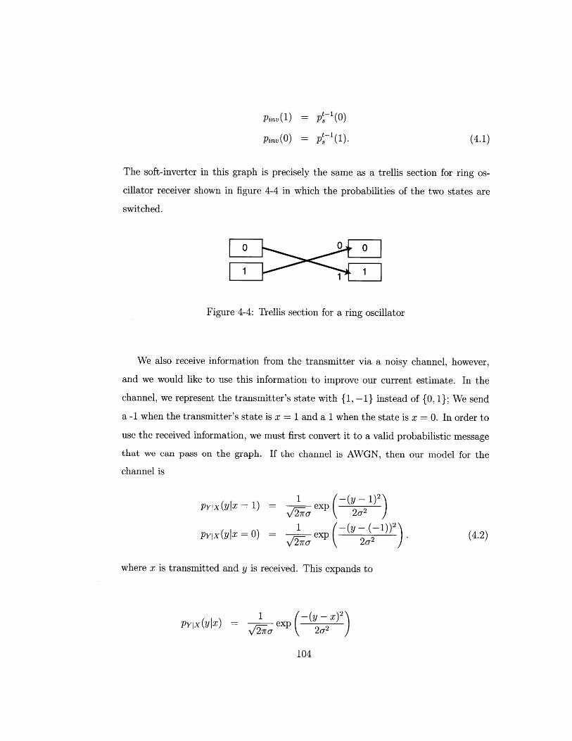
pin() pt- 1(0)
Pinv(0) = PS(1). (4.1)
The soft-inverter in this graph is precisely the same as a trellis section for ring os-
cillator receiver shown in figure 4-4 in which the probabilities of the two states are
switched.
0 0 0
Figure 4-4: Trellis section for a ring oscillator
We also receive information from the transmitter via a noisy channel, however,
and we would like to use this information to improve our current estimate. In the
channel, we represent the transmitter's state with {1, -1} instead of {0, 1}; We send
a -1 when the transmitter's state is x = 1 and a 1 when the state is x = 0. In order to
use the received information, we must first convert it to a valid probabilistic message
that we can pass on the graph. If the channel is AWGN, then our model for the
channel is
PYx(yIx 1) = exp
PYIX(yIx 0) = exp (y 2 1))2 (4.2)
where x is transmitted and y is received. This expands to
1 -- (y - X)2pyix(yjx) = exp ((2u2
104
1 -(y -2-2xY + x 2 )PYlx(ylz) =7-exp 2.
PYlx(ylx) = exp 22 exp 2 exp . (4.3)
If we assume that a is fixed, then for a given received value of y the e-1 2 /2,2 terms
will normalize out. Equation (4.1.1) then becomes
PY|X(yIx) = 2 eXp eXp (4.4)
where -y is a normalization constant. If we further assume that the channel is properly
equalized so that |xl = 1 (as we have been doing) then the eX2/20, 2 terms will also
normalize out leaving
PYIx(ylx) = -yexp(yx). (4.5)
We can write the message from the channel model node as
py (1) = exp (-1 - y)
py(0) = exp (1. y) . (4.6)
Thus we see that for a properly equalized, binary, AWGN channel with known sigma,
the channel model computation reduces essentially to an inner product of the received
value with the possible transmitted symbols.
We need to combine the estimate from the received signal which has been modified
by the channel model with the message from the soft-inverter in order to produce the
current state estimate, st. As for any variable node with multiple incoming messages,
the state nodes do this by performing an element by element product of the incoming
messages and then normalizing. The resulting message output from the state node st
105
is therefore
ps(1) = p 1 (0)pyIx(yIX = 1)
p's(0) =pS-,(1)pylx(ylz = 0)
4.1.2 Forward-only Message Passing on the Ring Oscillator
Trellis
Notice that the messages we pass in the trellis factor graph in figure 4-4 are only sent to
the right on the trellis factor graph - from past states to future states. This is because
we are only interested in the current state of the transmitter, and there is no way to
improve our estimate of the current state by adding any backward message passing.
Furthermore if we have perfectly estimated the current state of the transmitter there
is no reason to send messages backward to improve our estimates of past states of
the transmitter. Knowing the current state of a deterministic transmitter gives us
complete information about the history of the transmitter. We call this forward-only
message passing.
We can "roll up" the forward-only message passing on the trellis factor graph.
Examine figure 4-3 carefully. A given state node combines a message from the channel
model with (soft-inverted) message from the last state. Exactly the same message
calculations are performed by the factor graph on the right side of figure 4-5. So
forward-only message passing on the trellis receiver graph can itself be written to
closely resemble a ring oscillator. The only difference between this "receiver ring
oscillator" and the transmit ring oscillator is that the receiver oscillator includes a
channel model.
Note that the rolled up "factor graph" in figure figure 4-5, like many of the rolled
up factor graphs in this document, abuses the factor graph notation because messages
only travel in one direction on them. Also there should properly be a variable node in
between any two connected factor nodes. We have left out variable nodes with only
two incident edges which trivially pass messages without performing any computation.
106
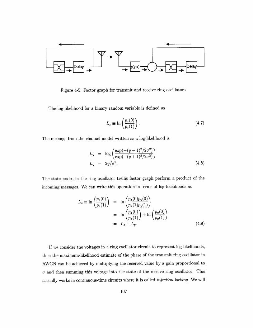
+
Figure 4-5: Factor graph for transmit and receive ring oscillators
The log-likelihood for a binary random variable is defined as
Lz ln (Pz(0) (4.7)
The message from the channel model written as a log-likelihood is
= log (exp(-(y - 1)2/2o.2)Y (exp(-(y + 1)2/20.2)
LY = 2y/a.2 . (4.8)
The state nodes in the ring oscillator trellis factor graph perform a product of the
incoming messages. We can write this operation in terms of log-likelihoods as
L=Inpz (0) Inpx(0)py (0)
=In ( ())+ In P()
= L+ LY. (4.9)
If we consider the voltages in a ring oscillator circuit to represent log-likelihoods,
then the maximum-likelihood estimate of the phase of the transmit ring oscillator in
AWGN can be achieved by multiplying the received value by a gain proportional to
a and then summing this voltage into the state of the receive ring oscillator. This
actually works in continuous-time circuits where it is called injection locking. We will
107
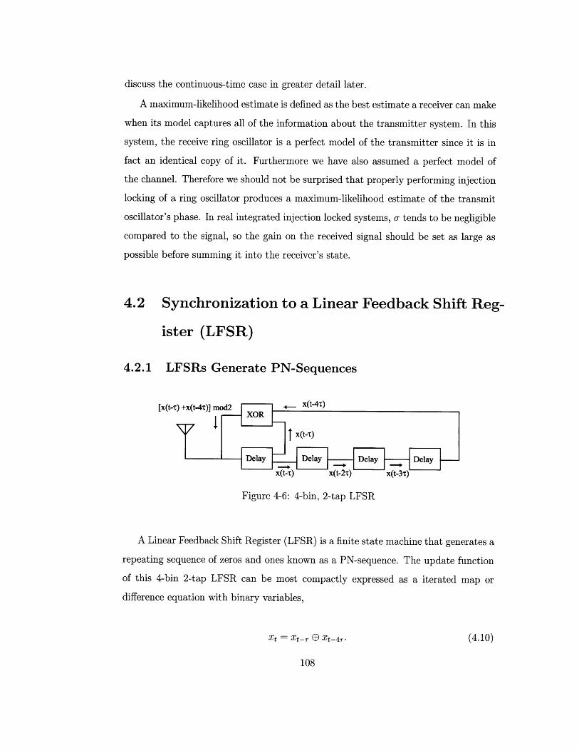
discuss the continuous-time case in greater detail later.
A maximum-likelihood estimate is defined as the best estimate a receiver can make
when its model captures all of the information about the transmitter system. In this
system, the receive ring oscillator is a perfect model of the transmitter since it is in
fact an identical copy of it. Furthermore we have also assumed a perfect model of
the channel. Therefore we should not be surprised that properly performing injection
locking of a ring oscillator produces a maximum-likelihood estimate of the transmit
oscillator's phase. In real integrated injection locked systems, o tends to be negligible
compared to the signal, so the gain on the received signal should be set as large as
possible before summing it into the receiver's state.
4.2 Synchronization to a Linear Feedback Shift Reg-
ister (LFSR)
4.2.1 LFSRs Generate PN-Sequences
[x(t-r) +x(t-4t)] mo2 x(t4r)
7 x(t-r)nDlay Dell ay ay---Delay -
x(t-t) x(t-2t) x(t-3t)
Figure 4-6: 4-bin, 2-tap LFSR
A Linear Feedback Shift Register (LFSR) is a finite state machine that generates a
repeating sequence of zeros and ones known as a PN-sequence. The update function
of this 4-bin 2-tap LFSR can be most compactly expressed as a iterated map or
difference equation with binary variables,
Xt = Xt-, @ xt-4,. (4.10)
108
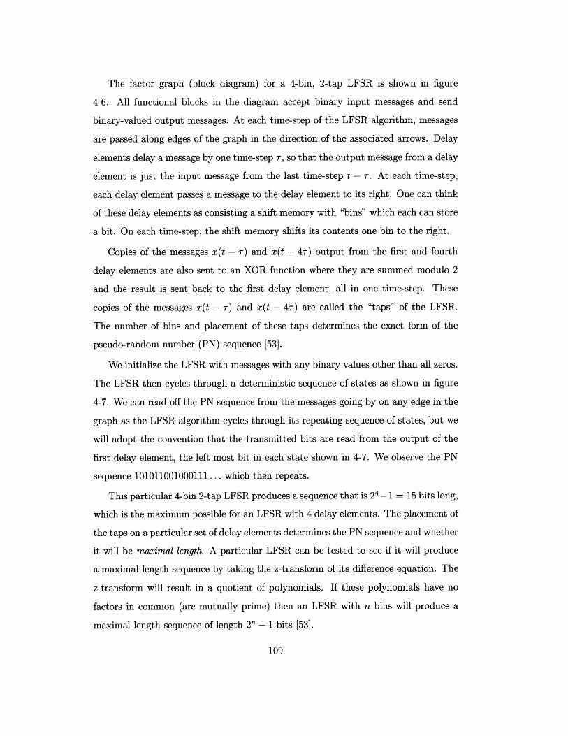
The factor graph (block diagram) for a 4-bin, 2-tap LFSR is shown in figure
4-6. All functional blocks in the diagram accept binary input messages and send
binary-valued output messages. At each time-step of the LFSR algorithm, messages
are passed along edges of the graph in the direction of the associated arrows. Delay
elements delay a message by one time-step T, so that the output message from a delay
element is just the input message from the last time-step t - r. At each time-step,
each delay element passes a message to the delay element to its right. One can think
of these delay elements as consisting a shift memory with "bins" which each can store
a bit. On each time-step, the shift memory shifts its contents one bin to the right.
Copies of the messages x(t - T) and x(t - 4T) output from the first and fourth
delay elements are also sent to an XOR function where they are summed modulo 2
and the result is sent back to the first delay element, all in one time-step. These
copies of the messages x(t - T) and x(t - 4T) are called the "taps" of the LFSR.
The number of bins and placement of these taps determines the exact form of the
pseudo-random number (PN) sequence [53].
We initialize the LFSR with messages with any binary values other than all zeros.
The LFSR then cycles through a deterministic sequence of states as shown in figure
4-7. We can read off the PN sequence from the messages going by on any edge in the
graph as the LFSR algorithm cycles through its repeating sequence of states, but we
will adopt the convention that the transmitted bits are read from the output of the
first delay element, the left most bit in each state shown in 4-7. We observe the PN
sequence 101011001000111 ... which then repeats.
This particular 4-bin 2-tap LFSR produces a sequence that is 24 -1 = 15 bits long,
which is the maximum possible for an LFSR with 4 delay elements. The placement of
the taps on a particular set of delay elements determines the PN sequence and whether
it will be maximal length. A particular LFSR can be tested to see if it will produce
a maximal length sequence by taking the z-transform of its difference equation. The
z-transform will result in a quotient of polynomials. If these polynomials have no
factors in common (are mutually prime) then an LFSR with n bins will produce a
maximal length sequence of length 2' - 1 bits [531.
109
0000
Figure 4-7: State cycle of a 4-bin, 2-tap LFSR
4.2.2 Applications of LFSR Synchronization
Why should we care about LFSR synchronization? In fact, LFSR synchronization
is a rather important function in many applications. For example, a Global Posi-
tioning System (GPS) receiver spends significant resources to achieve highly accu-
rate LFSR synchronization in a very low SNR environment. LFSR synchronization
(known as PN-sequence acquisition) is also an important problem in direct-sequence
code-division multiple access (DS/CDMA) communication such as is currently used
in IS-95 and 3G cell phone networks and wireless LAN systems.
The most ubiquitous circuit primitive currently used for synchronization is known
110
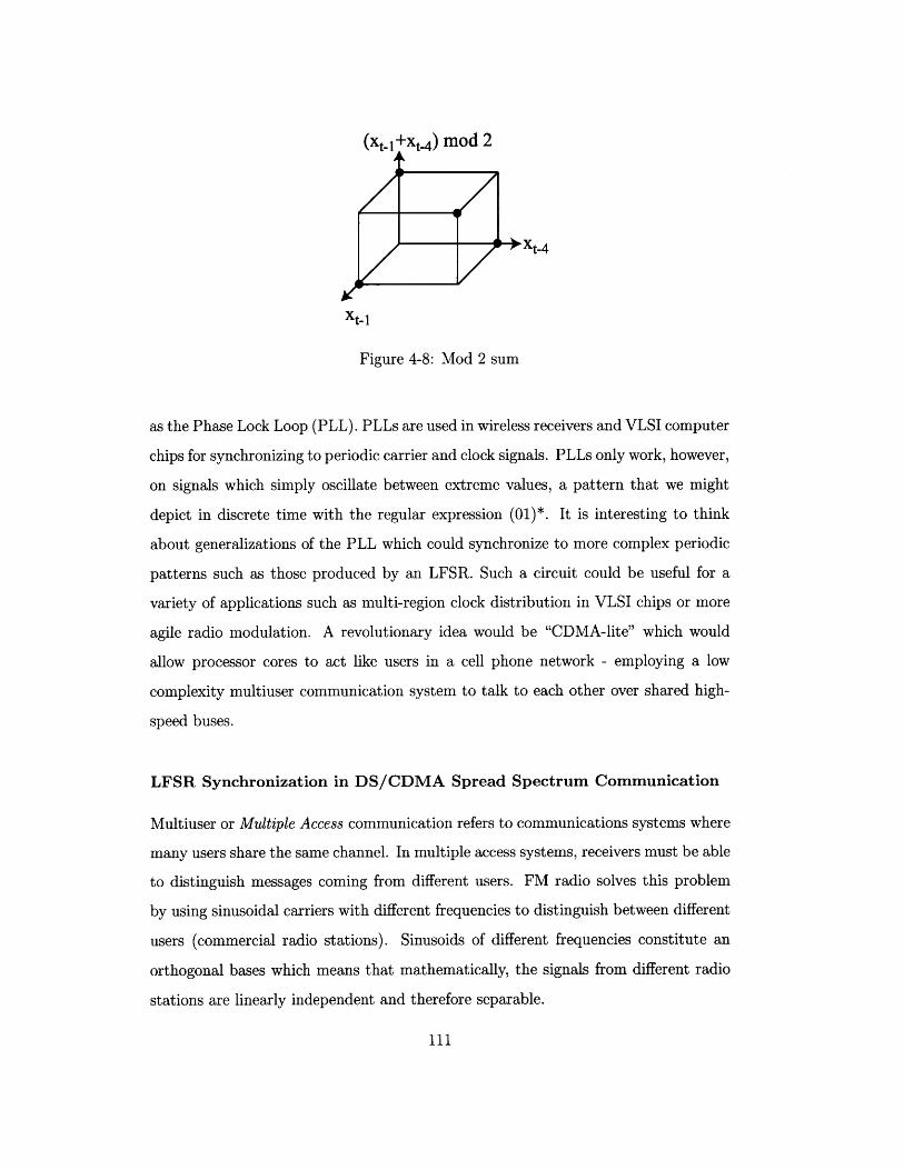
Xt-1
Figure 4-8: Mod 2 sum
as the Phase Lock Loop (PLL). PLLs are used in wireless receivers and VLSI computer
chips for synchronizing to periodic carrier and clock signals. PLLs only work, however,
on signals which simply oscillate between extreme values, a pattern that we might
depict in discrete time with the regular expression (01)*. It is interesting to think
about generalizations of the PLL which could synchronize to more complex periodic
patterns such as those produced by an LFSR. Such a circuit could be useful for a
variety of applications such as multi-region clock distribution in VLSI chips or more
agile radio modulation. A revolutionary idea would be "CDMA-lite" which would
allow processor cores to act like users in a cell phone network - employing a low
complexity multiuser communication system to talk to each other over shared high-
speed buses.
LFSR Synchronization in DS/CDMA Spread Spectrum Communication
Multiuser or Multiple Access communication refers to communications systems where
many users share the same channel. In multiple access systems, receivers must be able
to distinguish messages coming from different users. FM radio solves this problem
by using sinusoidal carriers with different frequencies to distinguish between different
users (commercial radio stations). Sinusoids of different frequencies constitute an
orthogonal bases which means that mathematically, the signals from different radio
stations are linearly independent and therefore separable.
111
11_--'," - fAR
Code Division multiple-access refers to the practice of distinguishing different users
with different bit sequences or codes. Direct-Sequence Code-Division Multiple Access
(DS/CDMA) wireless systems often use codes generated by LFSRs to distinguish
information transmitted by different users. A DS/CDMA transmitter and receiver
are shown in figures 4-9 and 4-10 respectively. The message signal is multiplied by
a PN-sequence generated by an LFSR. Since the different LFSR sequences may be
orthogonal but are at least uncorrelated, they too may serve as carriers which are
separable. Using a PN-sequence to directly modulate the message signal is called
Direct Sequence Code Division Multiple Access. Since a PN-sequence has a white
frequency spectrum, modulating the message signal by the PN-sequence has the effect
of spreading the message signal over a wide frequency range while reducing the amount
of power at any given frequency and is one method of producing a Spread-Spectrum
signal.
There are other methods for spreading the spectrum of a message signal. A popu-
lar alternative to CDMA is Frequency Domain Multiple Access (FDMA) in which we
periodically switch the frequency of a sinusoidal carrier. DS/CDMA has a number of
particular advantages over other techniques such as nice spectrum sharing properties
and resilience against jamming and multi-path interference.
LFSR synchronization in a DS/CDMA receiver is known as PN-sequence acquisi-
tion. In order to listen to a given user's message, the receiver must acquire that user's
LFSR so that it can remove it and recover the transmitted signal. The performance of
an acquisition system is measured in terms of its time to acquire and the repeatability
of this acquisition time. False positives are also a consideration. In a noncoherent
DS/CDMA system, acquisition is performed first, and then a tracking loop takes over
to maintain the receiver's LFSR in close alignment with the transmitter's LFSR.
112
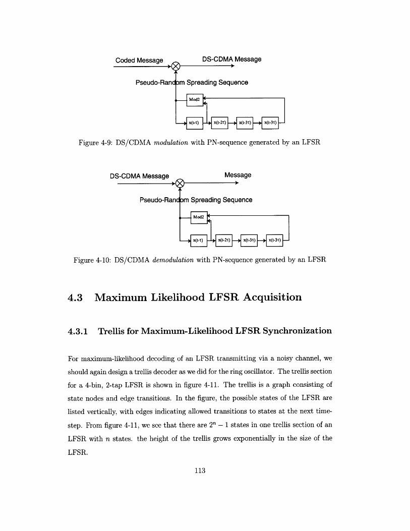
DS-CDMA Message
Figure 4-9: DS/CDMA modulation with PN-sequence generated by an LFSR
DS-CDMA Message Message
Pseudo-Rant
Figure 4-10: DS/CDMA demodulation with PN-sequence generated by an LFSR
4.3 Maximum Likelihood LFSR Acquisition
4.3.1 Trellis for Maximum-Likelihood LFSR Synchronization
For maximum-likelihood decoding of an LFSR transmitting via a noisy channel, we
should again design a trellis decoder as we did for the ring oscillator. The trellis section
for a 4-bin, 2-tap LFSR is shown in figure 4-11. The trellis is a graph consisting of
state nodes and edge transitions. In the figure, the possible states of the LFSR are
listed vertically, with edges indicating allowed transitions to states at the next time-
step. From figure 4-11, we see that there are 2" - 1 states in one trellis section of an
LFSR with n states. the height of the trellis grows exponentially in the size of the
LFSR.
113
Coded Message
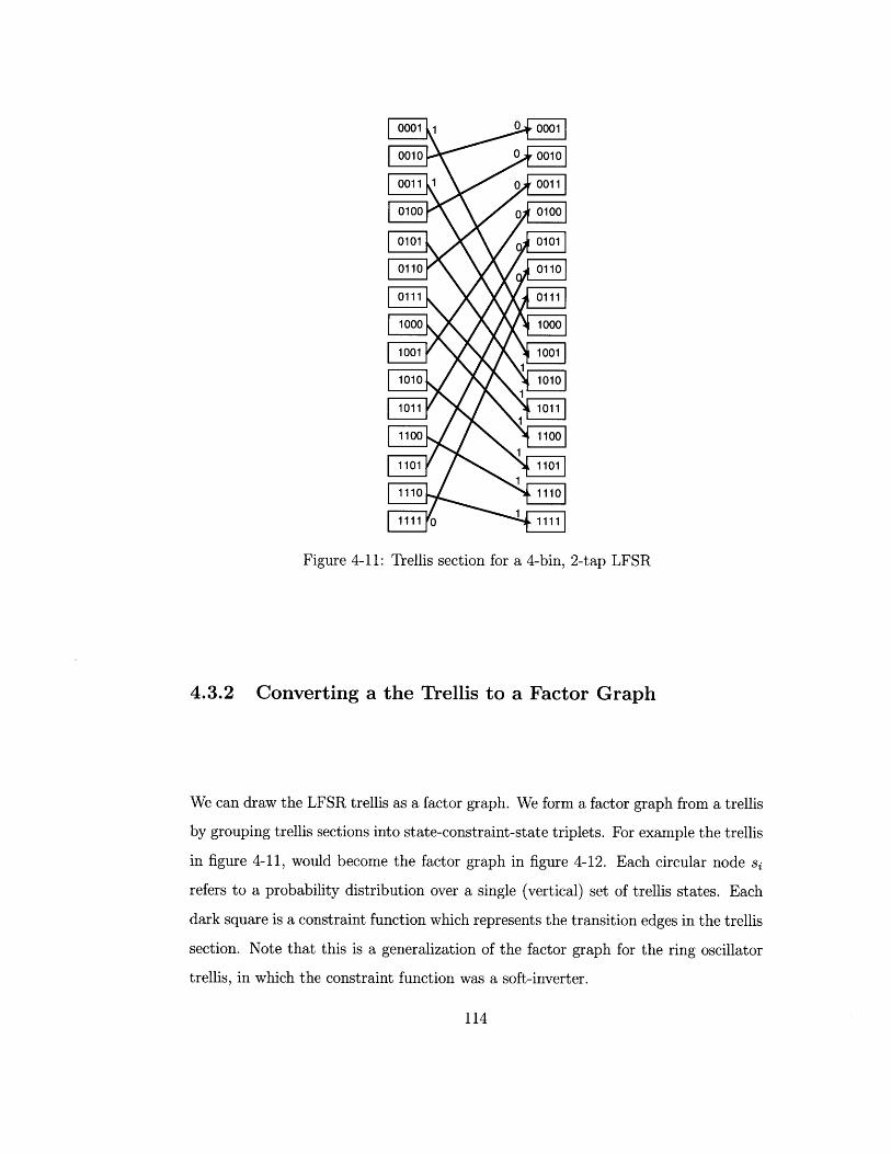
Figure 4-11: Trellis section for a 4-bin, 2-tap LFSR
4.3.2 Converting a the Trellis to a Factor Graph
We can draw the LFSR trellis as a factor graph. We form a factor graph from a trellis
by grouping trellis sections into state-constraint-state triplets. For example the trellis
in figure 4-11, would become the factor graph in figure 4-12. Each circular node si
refers to a probability distribution over a single (vertical) set of trellis states. Each
dark square is a constraint function which represents the transition edges in the trellis
section. Note that this is a generalization of the factor graph for the ring oscillator
trellis, in which the constraint function was a soft-inverter.
114
._III___.__II-I_"_.-'_".I - ----
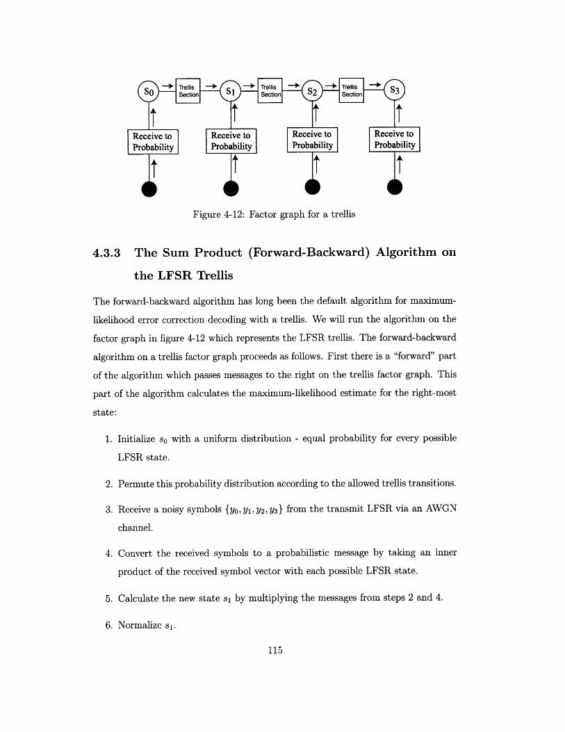
Figure 4-12: Factor graph for a trellis
4.3.3 The Sum Product (Forward-Backward) Algorithm on
the LFSR Trellis
The forward-backward algorithm has long been the default algorithm for maximum-
likelihood error correction decoding with a trellis. We will run the algorithm on the
factor graph in figure 4-12 which represents the LFSR trellis. The forward-backward
algorithm on a trellis factor graph proceeds as follows. First there is a "forward" part
of the algorithm which passes messages to the right on the trellis factor graph. This
part of the algorithm calculates the maximum-likelihood estimate for the right-most
state:
1. Initialize so with a uniform distribution - equal probability for every possible
LFSR state.
2. Permute this probability distribution according to the allowed trellis transitions.
3. Receive a noisy symbols {yo, Y1, Y2, Y3} from the transmit LFSR via an AWGN
channel.
4. Convert the received symbols to a probabilistic message by taking an inner
product of the received symbol vector with each possible LFSR state.
5. Calculate the new state si by multiplying the messages from steps 2 and 4.
6. Normalize si.
115
7. Repeat: At each time-step, move to the right on the trellis, updating the state
probability with information from each successively received symbol.
Then there is a backward part of the algorithm which passes messages to the left
on the trellis factor graph. This part of the algorithm improves the state estimates
of all of the states to the left of the right-most state, so that the end result is that
every state in the trellis factor graph contains a maximum-likelihood estimate:
1. Initialize with the most recent (right-most) probability distribution over the
trellis states, Stmax.
2. Pass this message to the left through the trellis section.
3. Combine the left-going message from the trellis section with information from
the most recently received (right-most) symbol from the channel.
4. Normalize the state.
5. Repeat: At each time-step, move to the left on the trellis.
It should be clear by now that the forward-backward algorithm is just the sum-
product algorithm operating on the factor graph for a trellis. Since this graph is a
tree, the sum-product algorithm will be exact and will produce maximum-likelihood
estimates.
As in the ring oscillator example, there is no need for us to perform the backward
step of the algorithm for this synchronization task. If we have a maximum-likelihood
estimate in the right-most state, that gives us a maximum-likelihood estimate of the
current state of the transmitter. The transmit LFSR is deterministic, so the trellis
for any LFSR has only one edge emanating from any given state and only one way to
transition between states. Therefore if we are given the most likely state in the right-
most trellis section, this in turn gives us complete information about the history of
the (deterministic) transmitter. The forward part of the algorithm suffices to recover
the most likely history of the transmit LFSR.
116
In effect, the trellis synchronizer correlates every possible state with the received
signal at every time-step. This computation is exponentially complex in the number of
bins of the transmit LFSR. In practice, this parallel correlation operation is serialized
and combined with decision theory to conserve resources. But reduced computational
complexity comes at the expense of longer and unpredictable acquisition times [32].
4.3.4 The Max Product (Viterbi's) Algorithm
Many electrical engineers will have a passing familiarity with Viterbi's algorithm.
Viterbi's algorithm is nearly identical to the forward-backward algorithm, but instead
of storing a "soft" probability distribution at each time-step, Viterbi's algorithm picks
the most likely state at each time-step and then assumes that it is 100% likely. So
Viterbi's algorithm doesn't have to store a probability distribution over all the trellis
states, it only has to store the most likely trellis state. Using this max operation
instead of a sum operation is a different (less memory intensive) way of summarizing
the information about which path through the trellis is most likely so far. The Viterbi
algorithm is therefore also known as the max product algorithm.
Since multiplication is distributive over the max function just as it is distributive
over the sum function, the operations still form a semi-ring as they do in the sum
product (forward-backward) algorithm. In general we can use any summary function
which forms a semi-ring with multiplication. The distributive property of a semi-ring
assures us that we are still able to distribute products over the summary function,
which is the pre-requisite for being able to express recursive concatenation of products
and summary functions as local message passing on a graph.
4.4 Low-Complexity LFSR Acquisition
4.4.1 The LFSR Shift Graph
Though the trellis factor graph is optimum in the sense that it performs a maximum-
likelihood estimate, it is not the only graph we can draw for synchronizing the LFSR.
117
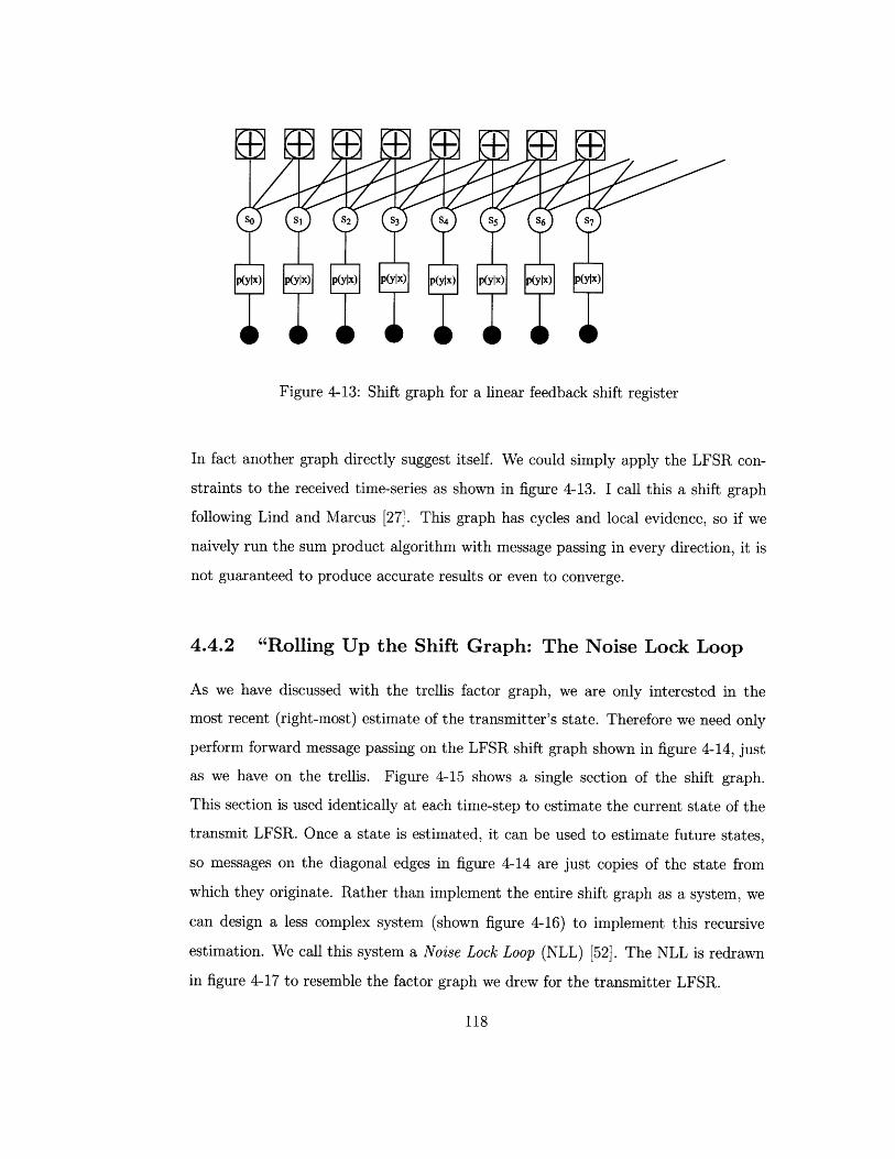
Figure 4-13: Shift graph for a linear feedback shift register
In fact another graph directly suggest itself. We could simply apply the LFSR con-
straints to the received time-series as shown in figure 4-13. I call this a shift graph
following Lind and Marcus [27]. This graph has cycles and local evidence, so if we
naively run the sum product algorithm with message passing in every direction, it is
not guaranteed to produce accurate results or even to converge.
4.4.2 "Rolling Up the Shift Graph: The Noise Lock Loop
As we have discussed with the trellis factor graph, we are only interested in the
most recent (right-most) estimate of the transmitter's state. Therefore we need only
perform forward message passing on the LFSR shift graph shown in figure 4-14, just
as we have on the trellis. Figure 4-15 shows a single section of the shift graph.
This section is used identically at each time-step to estimate the current state of the
transmit LFSR. Once a state is estimated, it can be used to estimate future states,
so messages on the diagonal edges in figure 4-14 are just copies of the state from
which they originate. Rather than implement the entire shift graph as a system, we
can design a less complex system (shown figure 4-16) to implement this recursive
estimation. We call this system a Noise Lock Loop (NLL) [52]. The NLL is redrawn
in figure 4-17 to resemble the factor graph we drew for the transmitter LFSR.
118
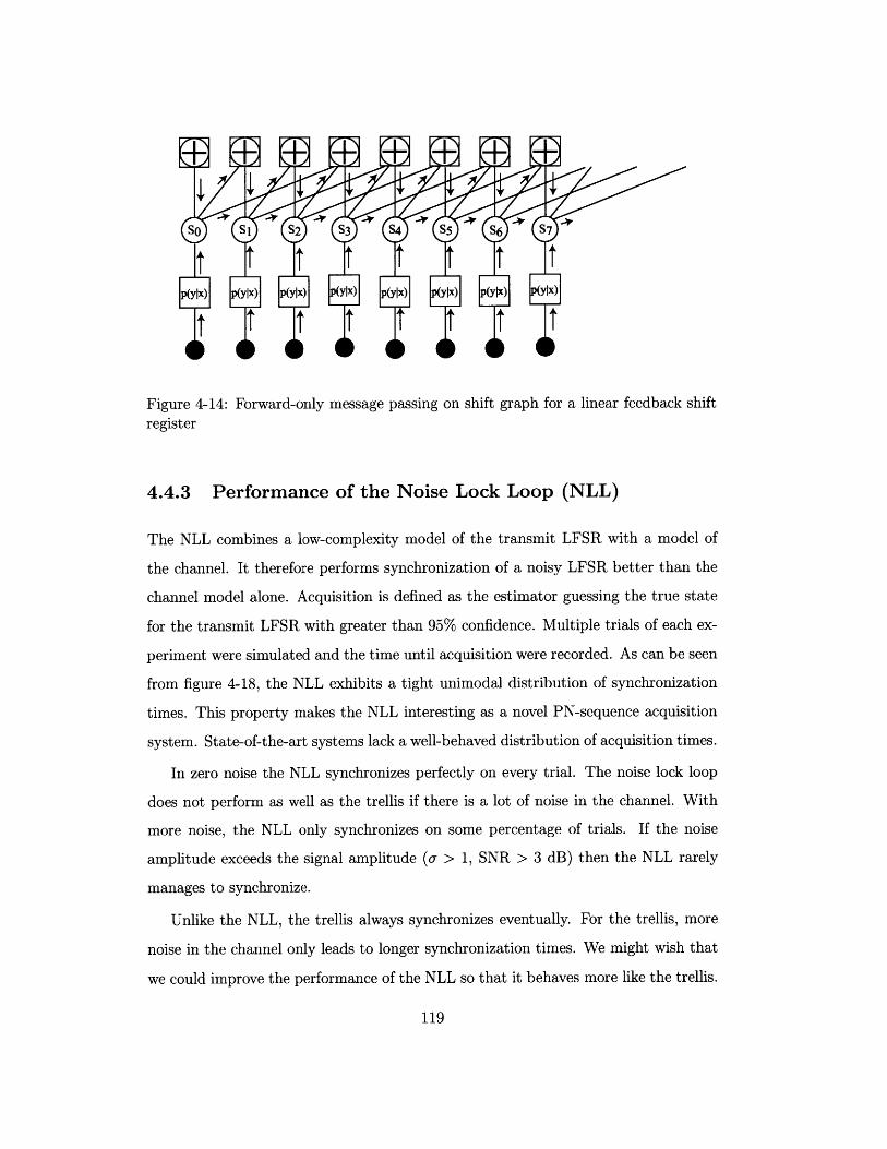
Figure 4-14: Forward-only message passing on shift graph for a linear feedback shiftregister
4.4.3 Performance of the Noise Lock Loop (NLL)
The NLL combines a low-complexity model of the transmit LFSR with a model of
the channel. It therefore performs synchronization of a noisy LFSR better than the
channel model alone. Acquisition is defined as the estimator guessing the true state
for the transmit LFSR with greater than 95% confidence. Multiple trials of each ex-
periment were simulated and the time until acquisition were recorded. As can be seen
from figure 4-18, the NLL exhibits a tight unimodal distribution of synchronization
times. This property makes the NLL interesting as a novel PN-sequence acquisition
system. State-of-the-art systems lack a well-behaved distribution of acquisition times.
In zero noise the NLL synchronizes perfectly on every trial. The noise lock loop
does not perform as well as the trellis if there is a lot of noise in the channel. With
more noise, the NLL only synchronizes on some percentage of trials. If the noise
amplitude exceeds the signal amplitude (a > 1, SNR > 3 dB) then the NLL rarely
manages to synchronize.
Unlike the NLL, the trellis always synchronizes eventually. For the trellis, more
noise in the channel only leads to longer synchronization times. We might wish that
we could improve the performance of the NLL so that it behaves more like the trellis.
119
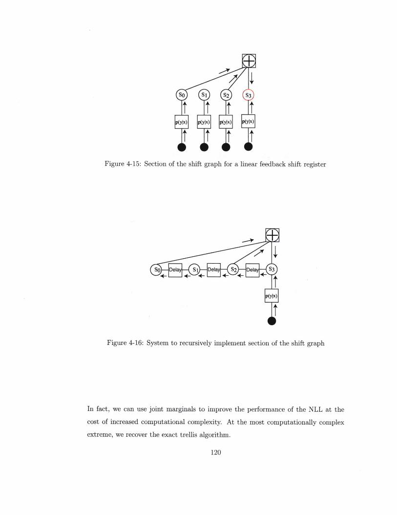
Figure 4-15: Section of the shift graph for a linear feedback shift register
Figure 4-16: System to recursively implement section of the shift graph
In fact, we can use joint marginals to improve the performance of the NLL at the
cost of increased computational complexity. At the most computationally complex
extreme, we recover the exact trellis algorithm.
120
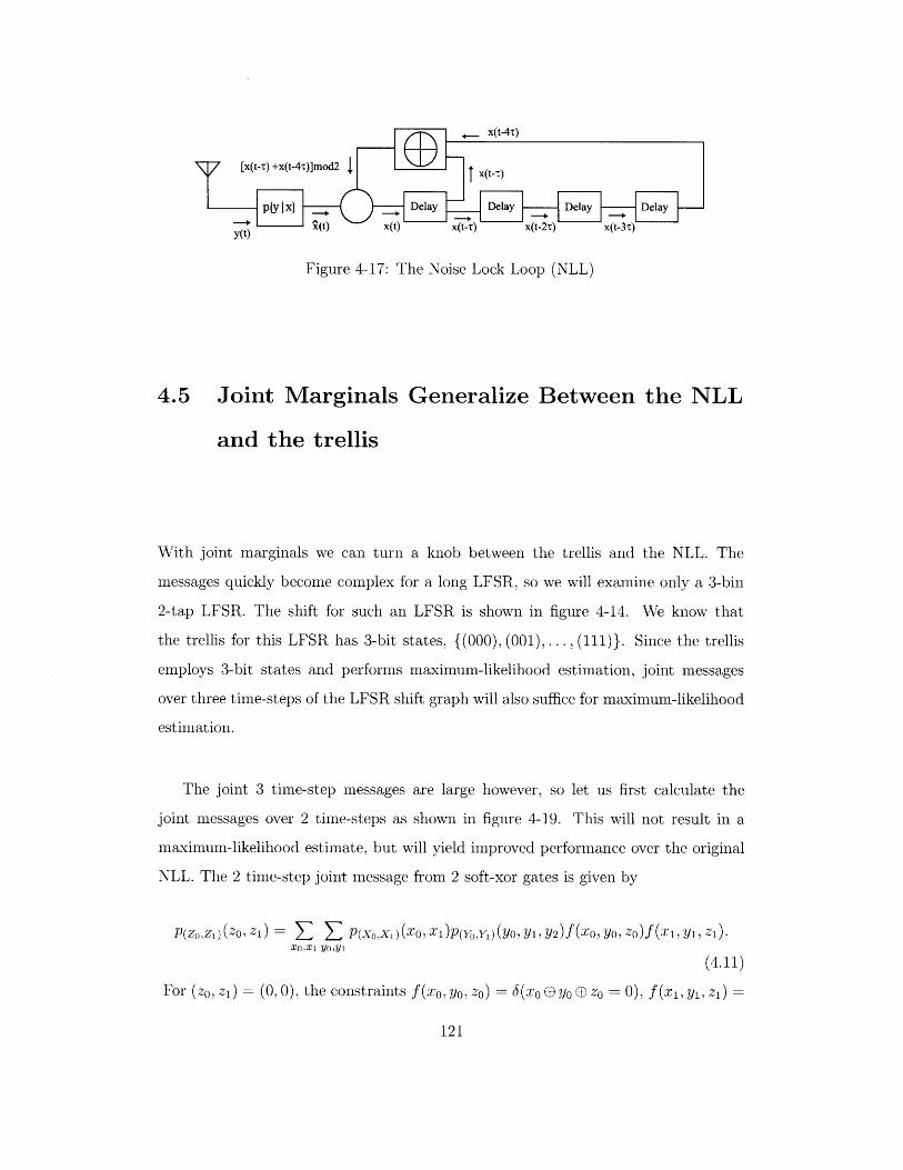
Figure 4-17: The Noise Lock Loop (NLL)
4.5 Joint Marginals Generalize Between the NLL
and the trellis
With joint marginals we can turn a knob between the trellis and the NLL. The
messages quickly become complex for a long LFSR, so we will examine only a 3-bin
2-tap LFSR. The shift for such an LFSR is shown in figure 4-14. We know that
the trellis for this LFSR has 3-bit states, {(000), (001),. .. , (111)}. Since the trellis
employs 3-bit states and performs maximum-likelihood estimation, joint messages
over three time-steps of the LFSR shift graph will also suffice for maximum-likelihood
estimation.
The joint 3 time-step messages are large however, so let us first calculate the
joint messages over 2 time-steps as shown in figure 4-19. This will not result in a
maximum-likelihood estimate, but will yield improved performance over the original
NLL. The 2 time-step joint message from 2 soft-xor gates is given by
P(Zo,Z1)(ZO, Zi) = 1Z P(Xo,XI)(zO, X)P(Y ,Y)(YO, Y1, Y 2)f (Xo, yo, Zo)f (Xi, y, Zi).X0,X1 yOY1
(4.11)
For (zo, zi) = (0, 0), the constraints f(xo, yo, zo) = (xo yo (D zo = 0), f (Xi, yi, zi) =
121
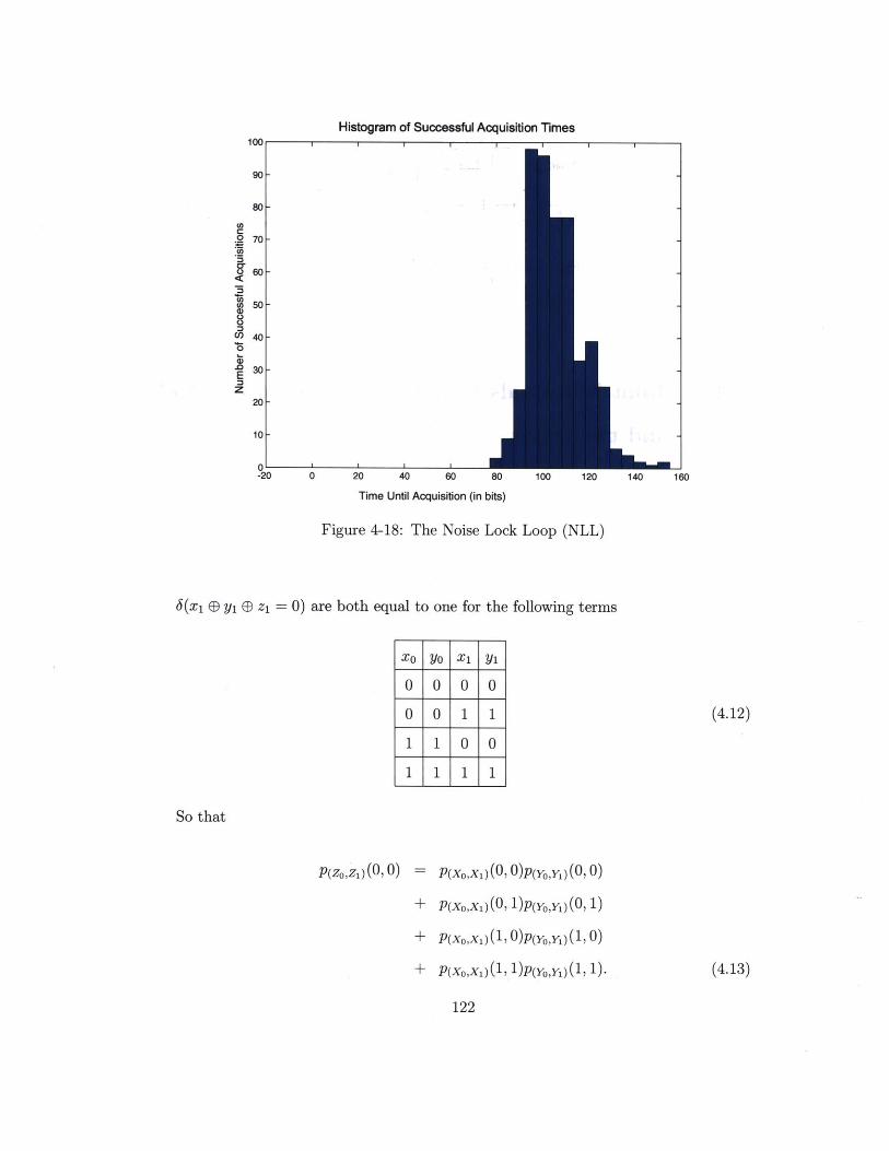
Histogram of Successful Acquisition Timesinn.
-20 0 20 40 60 80
Time Until Acquisition (in bits)
Figure 4-18: The Noise Lock
100 120 140 160
Loop (NLL)
6(xi E y E z1= 0) are both equal to one for the
X0 Yo X1 Yi
0 0 0 0
0 0 1 1
1 1 0 0
1 1 1 1
following terms
(4.12)
So that
P(Zo,zi)(0, 0) = P(xo,x1)(0, 0)pOy 0,yo)(0, 0)
+ P(Xo,X1)(0, 1)p(y,y)(0, 1)
+ P(xe,x)(1, O)p(yo,y)(1, 0)
+ p(Xo,X1 )(1, 1)P(yo,y1)(1, 1).
122
(4.13)
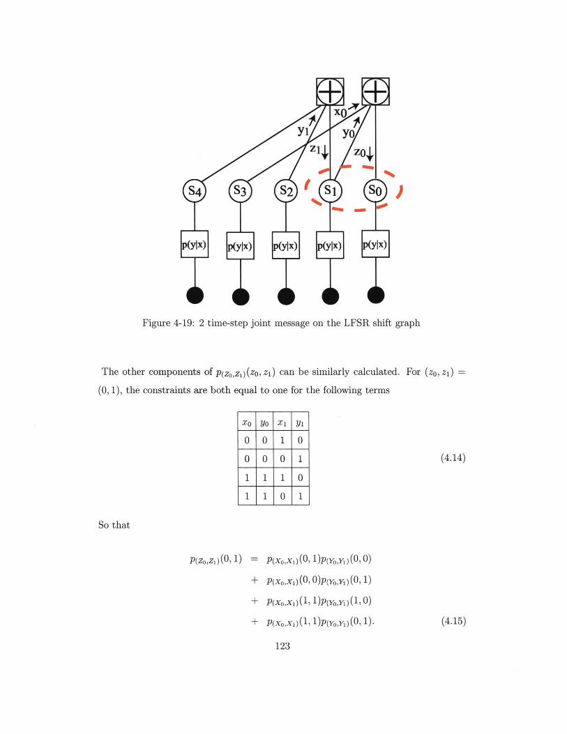
Figure 4-19: 2 time-step joint message on the LFSR shift graph
The other components of p(zo,zi) (zo, zi) can be similarly calculated. For (zo, zi) =
(0, 1), the constraints axe both equal to one for the following terms
X0 YA Xi Yi
0 0 1 0
0 0 0 1 (4.14)
1 1 1 0
1 1 0 1
So that
P(Zo,zi)(0, 1) =
+
+
+
P(Xo,X1)(0, l)p(YoY 1)(O, 0)
P(Xo,X1)(O, 0)p(Yoy 1)(0, 1)
P(xo,x1)(1, 1)p(yoy1)(1, 0)
P(Xo,X 1) (I, 1)p(yoy 1) (0, 1).
123
(4.15)
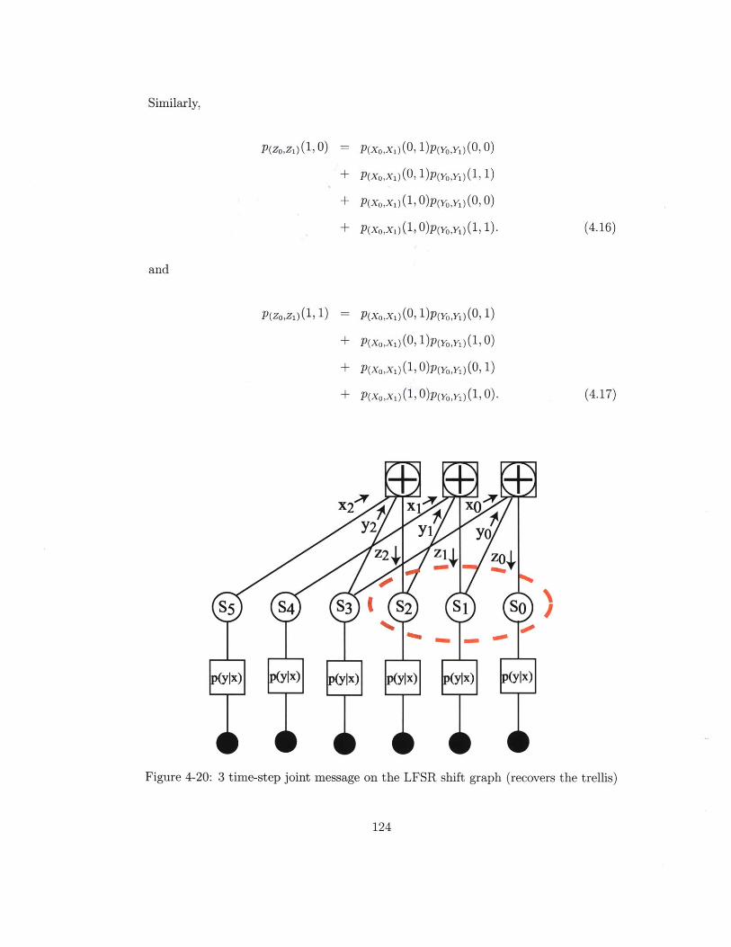
P(ZoZi)(1, 0)
P(Zo~zi)(1, 1)
P(Xo,X1 )(0, 1)p(yo,y1)(0, 0)
P(Xo,X1 )(0, 1)P(YoY 1)(1, 1)
P(Xo,X1 )(1, 0)P(yo,y1)(0, 0)
P(Xo,X1 )(1, 0)P(yo,y1)(1, 1).
P(Xo,X 1 )(0, l)P(yo,y1)(0, 1)
P(Xo,X1)(0, 1)p(Yo,Y1)(1, 0)
P(Xo,X 1)(1, O)P(yo,y1)(0, 1)
P(Xo,X 1)(1, O)P(yo,y1)(1, 0).
Figure 4-20: 3 time-step joint message on the LFSR shift graph (recovers the trellis)
124
Similarly,
and
(4.16)
(4.17)
Now let us calculate the 3 time-step joint message.
P(Zo,Zi,Z 2)(ZO, Z1, Z2) = E P(Xo,X 1 ,X2)(XOXiX2)P(Yo,Y,Y 2)(YOY 1,Y 2)XO ,X1,X2 YO,Y1,2
f(Xo, yo, zo)f(x1, y1, z1)f(x2, Y2, z2). (4.18)
For (zO, z1 , z2 ) = (0, 0, 0), the constraints f(xo, yo, zo) = 6(xo @ yo e zo = 0),
f(xiyizi) = 6(x1 E y1 e z1 = 0), and f(x2,Y2,z2) = 6(X2 e Y2 e z2 = 0) are
all equal to one for the following terms
zO X1 X2 Yo Y1 Y2
0 0 0 0 0 0
0 0 1 0 0 1
0 1 0 0 1 0
0 1 1 0 1 1
1 0 0 1 0 0
1 0 1 1 0 1
1 1 0 11 0
1 1 1 1 1 1
(4.19)
P(zo,zi,z2)(O, 0>,0) =
+-
+±
+±
+±
+±
+
+±
P(Xo,X 1 ,X2)(0, 0, 0)P(yo,y1,y2)(0, 0, 0)
P(Xo,X1,X 2)(0, 0, 1)P(yo,yi,y2)(0, 0, 1)
P(X,X1,X2) (0, 1, 0)p(yO,y1,y2) (0, 1, 0)
P(Xo,X1,X2) (0> 1, l)P(Yo,Yi,Y2) (0, 1, 1)
P(Xo,X1,X2) (1, 0 0)P(yo,y1,y2) (I, 0, 0)
P(Xo,X1,X 2) (1, 0, 1)P(yo,y1,y2) (1, 0, 1)
P(X,X1,X2) (1, 1, 0)P(yo,yi,y2) (1, 1, 0)
P(Xo,X1,X2)(, 1, 1)P(yo,y1,y2)(1, 1, 1).
125
So that
(4.20)
The other components of p(zo,zlz 2)(zo, z 1 , z 2 ) can be similarly calculated, but in the
interest of space will be left to the reader.
If we want to implement LFSR synchronization with these joint messages, on
each iteration of the algorithm the x message is the z message from 3 time-steps
before, PXOXX 2 ) (XO, x 1 , x 2 ) = P-zz2) (zo, zi, z2 ). Meanwhile the y message is the
z message from the last time-step, ptXOXX X1(o, x1, x 2 ) =Pzi,zz)(zo, zi, z 2 ).
4.6 Scheduling
To run the sum product algorithm in discrete-time on any graph, we must choose
an order in which to update the messages. We will assume that there is at most
one message transmitted in each direction on a given edge during a single time-step.
That message completely replaces any message that was being passed on that edge
in that direction at previous time-steps. As we have seen in earlier chapters, a new
outgoing message on one edge of a given node is calculated from local information,
from incoming messages on the other edges of the node. We define a message as
pending if it has been re-calculated due to new incoming messages.
A schedule could be chosen to allow all messages to be re-sent on all edges at each
time-step, whether they are pending (have changed) or not. This is called a flooding
schedule. However, we can accomplish exactly the same thing by only sending every
pending message in the graph on every time-step. This is the most aggressive possible
schedule for message passing. At the other extreme is a serial schedule, in which a
single pending message in the graph is chosen at random to be sent at each time-step.
In a cycle-free graph, with a schedule in which only pending messages are transmitted,
the sum product algorithm will eventually halt in a state with no messages pending.
If a graph has cycles, messages will continue to circulate around cycles in the graph
even if their values are no longer changing.
126
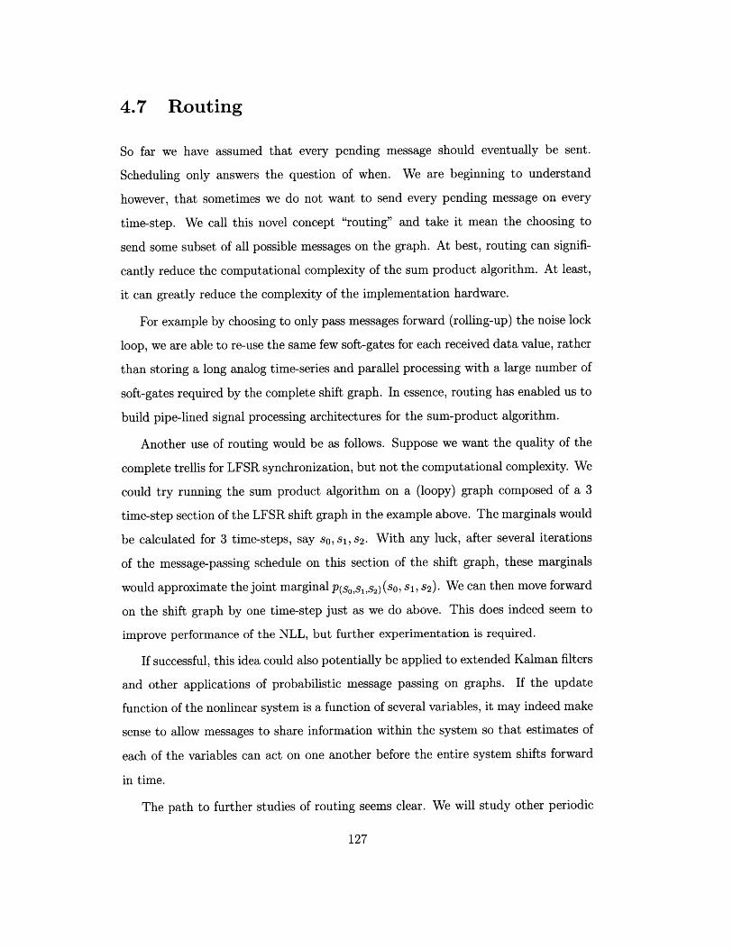
4.7 Routing
So far we have assumed that every pending message should eventually be sent.
Scheduling only answers the question of when. We are beginning to understand
however, that sometimes we do not want to send every pending message on every
time-step. We call this novel concept "routing" and take it mean the choosing to
send some subset of all possible messages on the graph. At best, routing can signifi-
cantly reduce the computational complexity of the sum product algorithm. At least,
it can greatly reduce the complexity of the implementation hardware.
For example by choosing to only pass messages forward (rolling-up) the noise lock
loop, we are able to re-use the same few soft-gates for each received data value, rather
than storing a long analog time-series and parallel processing with a large number of
soft-gates required by the complete shift graph. In essence, routing has enabled us to
build pipe-lined signal processing architectures for the sum-product algorithm.
Another use of routing would be as follows. Suppose we want the quality of the
complete trellis for LFSR synchronization, but not the computational complexity. We
could try running the sum product algorithm on a (loopy) graph composed of a 3
time-step section of the LFSR shift graph in the example above. The marginals would
be calculated for 3 time-steps, say so, Si, s2. With any luck, after several iterations
of the message-passing schedule on this section of the shift graph, these marginals
would approximate the joint marginal p(sos 1,s,2 ) (So, si, 2 ). We can then move forward
on the shift graph by one time-step just as we do above. This does indeed seem to
improve performance of the NLL, but further experimentation is required.
If successful, this idea could also potentially be applied to extended Kalman filters
and other applications of probabilistic message passing on graphs. If the update
function of the nonlinear system is a function of several variables, it may indeed make
sense to allow messages to share information within the system so that estimates of
each of the variables can act on one another before the entire system shifts forward
in time.
The path to further studies of routing seems clear. We will study other periodic
127
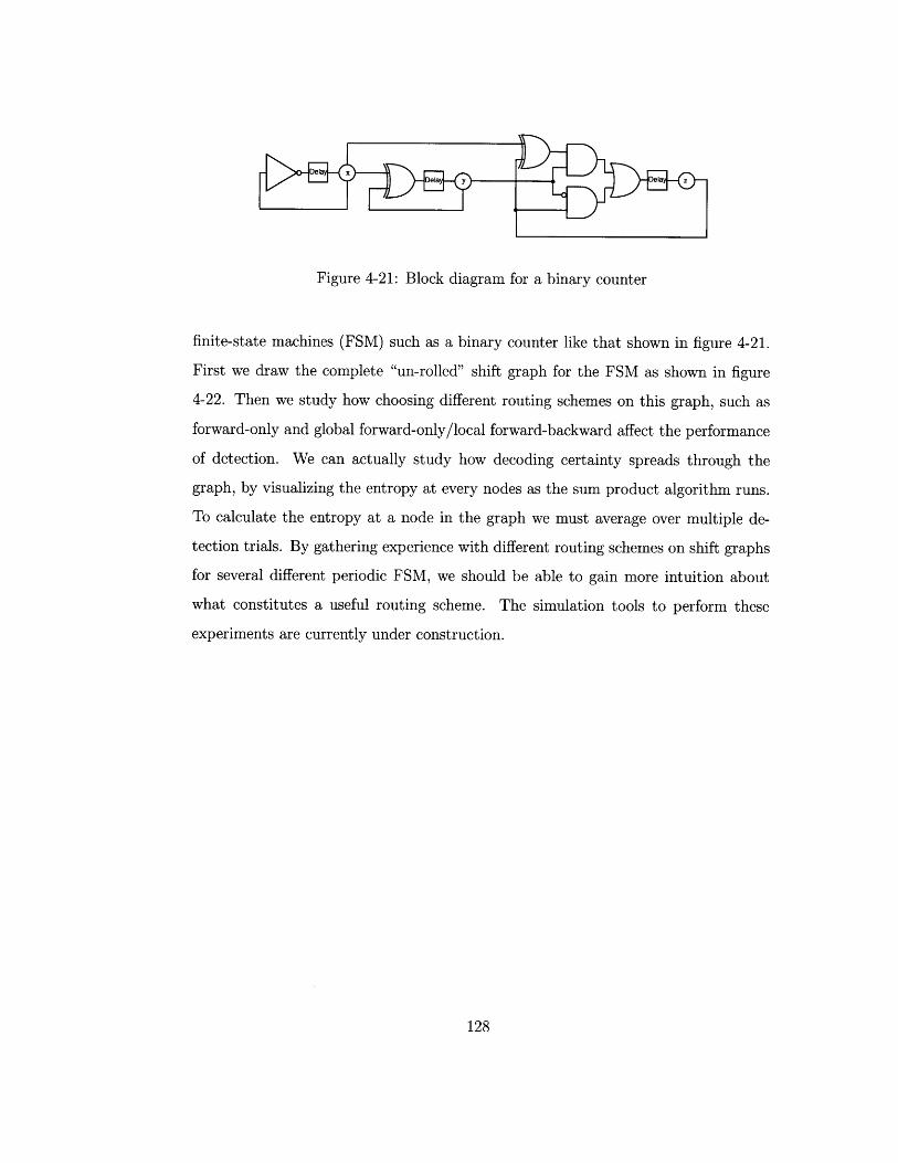
Figure 4-21: Block diagram for a binary counter
finite-state machines (FSM) such as a binary counter like that shown in figure 4-21.
First we draw the complete "un-rolled" shift graph for the FSM as shown in figure
4-22. Then we study how choosing different routing schemes on this graph, such as
forward-only and global forward-only/local forward-backward affect the performance
of detection. We can actually study how decoding certainty spreads through the
graph, by visualizing the entropy at every nodes as the sum product algorithm runs.
To calculate the entropy at a node in the graph we must average over multiple de-
tection trials. By gathering experience with different routing schemes on shift graphs
for several different periodic FSM, we should be able to gain more intuition about
what constitutes a useful routing scheme. The simulation tools to perform these
experiments are currently under construction.
128
Figure 4-22: Shift graph for a binary counter
129

130
Chapter 5
Analog VLSI Circuits for
Probabilistic Message Passing
5.1 Introduction: The Need for Multipliers
In order to build circuit implementations of the sum-product algorithm, we will need
circuits that compute products of parameters of probability distributions and cir-
cuits that sum over these parameters. Summing operations are trivial with currents,
because of Kirchoff's Current Law (KCL); one simply ties wires together to sum cur-
rents. Summing voltages is a bit more difficult, but one can use a summing amplifier.
Multiplication poses more choices for the designer. In this document we will inves-
tigate many of the most important ways to implement a multiply operation with
low-complexity analog transistor circuits.
An analog multiplier is a circuit which produces a scaled product Z of two inputs,
Z = kXY, (5.1)
where k is a scaling constant. The values of X, Y and Z can be represented by the
magnitude of a current or voltage. These values can also be represented by voltage
or current spikes or pulses; by the rate of repetition of a series of voltage spike
(pulse rate modulation or PRM), by the width of one or more spikes (pulse width
131
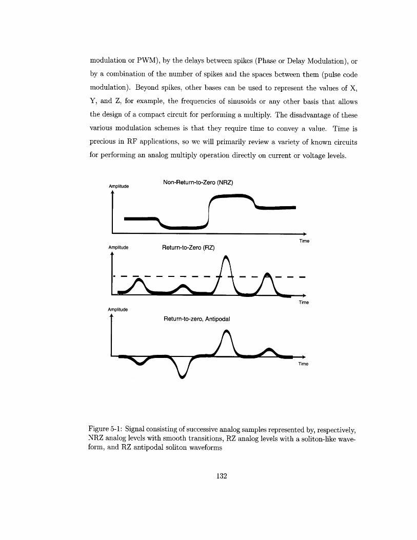
modulation or PWM), by the delays between spikes (Phase or Delay Modulation), or
by a combination of the number of spikes and the spaces between them (pulse code
modulation). Beyond spikes, other bases can be used to represent the values of X,
Y, and Z, for example, the frequencies of sinusoids or any other basis that allows
the design of a compact circuit for performing a multiply. The disadvantage of these
various modulation schemes is that they require time to convey a value. Time is
precious in RF applications, so we will primarily review a variety of known circuits
for performing an analog multiply operation directly on current or voltage levels.
Amplitude Non-Return-to-Zero (NRZ)
TimeAmplitude Return-to-Zero (RZ)
TimeAmplitude
Return-to-zero, Antipodal
%r Time
Figure 5-1: Signal consisting of successive analog samples represented by, respectively,NRZ analog levels with smooth transitions, RZ analog levels with a soliton-like wave-form, and RZ antipodal soliton waveforms
132
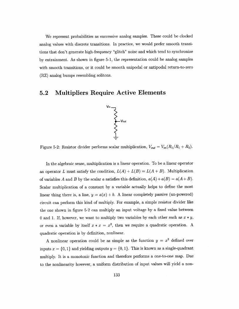
We represent probabilities as successive analog samples. These could be clocked
analog values with discrete transitions. In practice, we would prefer smooth transi-
tions that don't generate high-frequency "glitch" noise and which tend to synchronize
by entrainment. As shown in figure 5-1, the representation could be analog samples
with smooth transitions, or it could be smooth unipodal or antipodal return-to-zero
(RZ) analog bumps resembling solitons.
5.2 Multipliers Require Active Elements
vin
vout
Figure 5-2: Resistor divider performs scalar multiplication, Vo = Vin(R 1 /Ri + R 2 ).
In the algebraic sense, multiplication is a linear operation. To be a linear operator
an operator L must satisfy the condition, L(A) + L(B) = L(A + B). Multiplication
of variables A and B by the scalar a satisfies this definition, a(A) + a(B) = a(A + B).
Scalar multiplication of a constant by a variable actually helps to define the most
linear thing there is, a line, y = a(x) + b. A linear completely passive (un-powered)
circuit can perform this kind of multiply. For example, a simple resistor divider like
the one shown in figure 5-2 can multiply an input voltage by a fixed value between
0 and 1. If, however, we want to multiply two variables by each other such as x * y,
or even a variable by itself x * x = x2 , then we require a quadratic operation. A
quadratic operation is by definition, nonlinear.
A nonlinear operation could be as simple as the function y = x 2 defined over
inputs x = {0, 1} and yielding outputs y = {0, 1}. This is known as a single-quadrant
multiply. It is a monotonic function and therefore performs a one-to-one map. Due
to the nonlinearity however, a uniform distribution of input values will yield a non-
133
1-1-1.1111i -- - 1_1 1----____1_ __1_11_1__.-_.1__-_ -** - , , I - - ; - - - -_ - - - -___ - . , _ , - - -- - I __ - I .I I I I - -- l- _1 1. 1. . I - . - ___- - -, - -1 1 - __ - I - - - - -_ --
uniform distribution of output values compressed toward y = 0. Real valued voltages
that were evenly spaced apart over Vi,,, are now closer together in Vout. Physical
systems with finite energy which are measured over finite time, have finite resolution.
Because of this compression and the resolution limit, implementation of a single-
balanced multiply will erase some information about the input. Bennett's formulation
of Maxwell's Demon teaches us that it takes energy to erase information [25]. So a
single-quadrant multiply operation implemented by a physical system must dissipate
some amount of the energy. This energy can come from the input signal though, and
does not necessarily require an external power source.
Multipliers are often characterized as single quadrant (x > 0 and y > 0), double
quadrant (x > 0 or y 0) or four-quadrant (no restriction on the signs of x and y).
A four-quadrant multiply maps inputs between {-1, 1} to outputs between {-1, 1}.
It performs a many-to-one mapping from input state space to output state space,
meaning that different inputs can produce the same output, for example, (-1)(-1) =
1 and (1)(1) = 1. This many-to-one mapping erases an entire bit of information, the
sign of the input. We can see this because we would require the sign of at least
one input in order to reverse the operation. Therefore implementing a irreversible
four-quadrant multiply in a physical system requires power. All quadratic multiplier
circuit designs will use at least one active, powered circuit element.
We can approximate any nonlinear function with a Taylor series expansion. The
Taylor series expansion of a nonlinear function will include quadratic or higher order
terms. It will therefore require power to implement a nonlinear function in a physical
system. There is one special exception to this rule. It is possible to carefully construct
special multi-dimensional nonlinear functions which perform a one-to-one (unitary)
mapping and therefore do not require power when physically implemented.
134
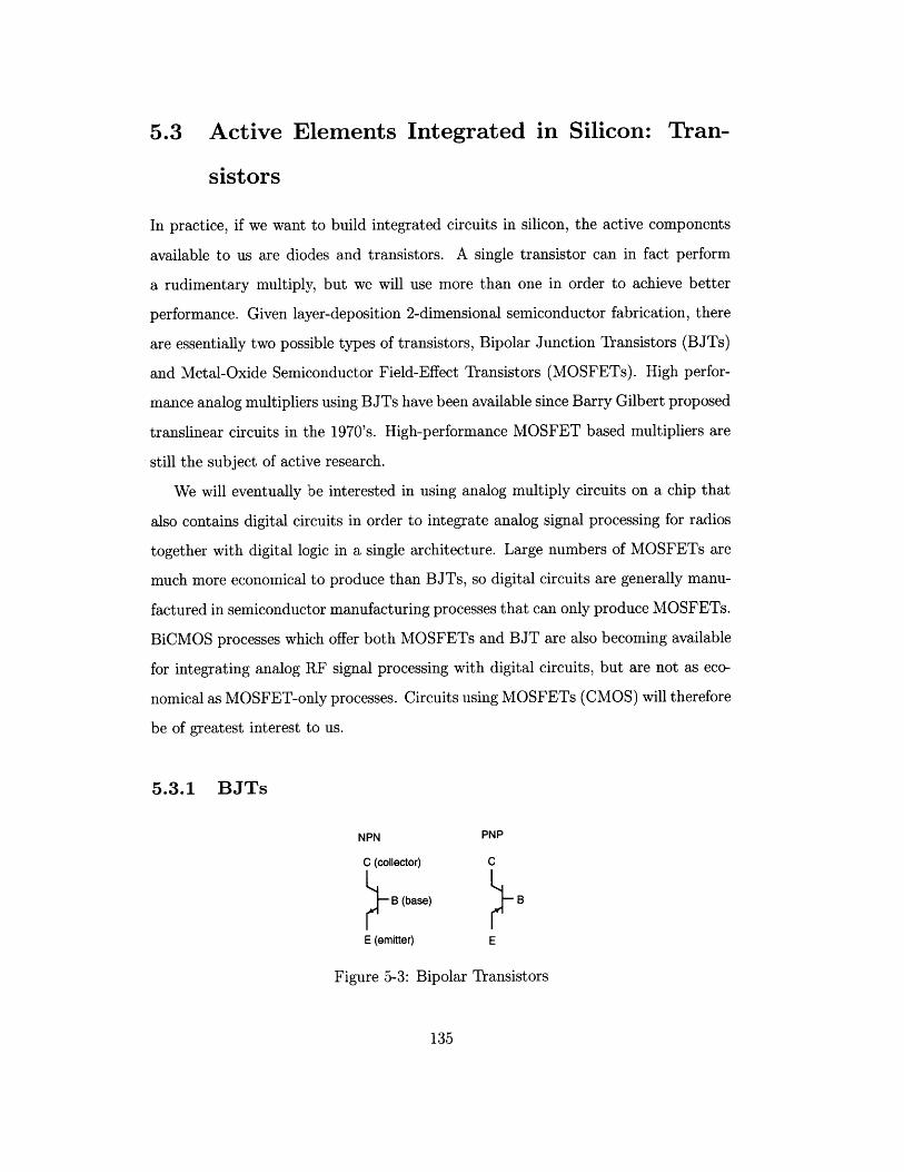
5.3 Active Elements Integrated in Silicon: Tran-
sistors
In practice, if we want to build integrated circuits in silicon, the active components
available to us are diodes and transistors. A single transistor can in fact perform
a rudimentary multiply, but we will use more than one in order to achieve better
performance. Given layer-deposition 2-dimensional semiconductor fabrication, there
are essentially two possible types of transistors, Bipolar Junction Transistors (BJTs)
and Metal-Oxide Semiconductor Field-Effect Transistors (MOSFETs). High perfor-
mance analog multipliers using BJTs have been available since Barry Gilbert proposed
translinear circuits in the 1970's. High-performance MOSFET based multipliers are
still the subject of active research.
We will eventually be interested in using analog multiply circuits on a chip that
also contains digital circuits in order to integrate analog signal processing for radios
together with digital logic in a single architecture. Large numbers of MOSFETs are
much more economical to produce than BJTs, so digital circuits are generally manu-
factured in semiconductor manufacturing processes that can only produce MOSFETs.
BiCMOS processes which offer both MOSFETs and BJT are also becoming available
for integrating analog RF signal processing with digital circuits, but are not as eco-
nomical as MOSFET-only processes. Circuits using MOSFETs (CMOS) will therefore
be of greatest interest to us.
5.3.1 BJTs
NPN PNP
C (collector) C
B (base) B
E (emitter) E
Figure 5-3: Bipolar Transistors
135
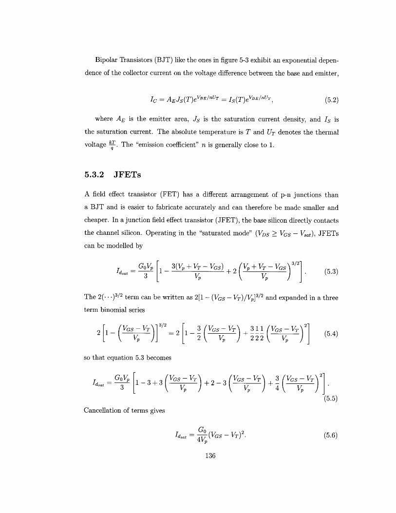
Bipolar Transistors (BJT) like the ones in figure 5-3 exhibit an exponential depen-
dence of the collector current on the voltage difference between the base and emitter,
Ic = AEJs(T)eVBEnUT V/Is(T)eBEnUT, (5.2)
where AE is the emitter area, JS is the saturation current density, and Is is
the saturation current. The absolute temperature is T and UT denotes the thermal
voltage k. The "emission coefficient" n is generally close to 1.q
5.3.2 JFETs
A field effect transistor (FET) has a different arrangement of p-n junctions than
a BJT and is easier to fabricate accurately and can therefore be made smaller and
cheaper. In a junction field effect transistor (JFET), the base silicon directly contacts
the channel silicon. Operating in the "saturated mode" (VDS > VGS - Vsat), JFETs
can be modelled by
GOVv F3(V+VT -VGS) p+VT - GS 3 /2ldsat - [IXp +2 . (5.3)
3 V V
The 2(. -)3/2 term can be written as 2[1 - (VGS - T) 3/2 and expanded in a three
term binomial series
VVS 3 (VGS - VT) + 311 VGSVT )2 (
so that equation 5.3 becomes
GOV/ VGSV- VT GS T + 3 (VGS- VT 2Idsat 1-3+3 +2-3 + .3 V V 4 V4
(5.5)
Cancellation of terms gives
_Go (Ia (VGS - T) 2 . (5.6)
136
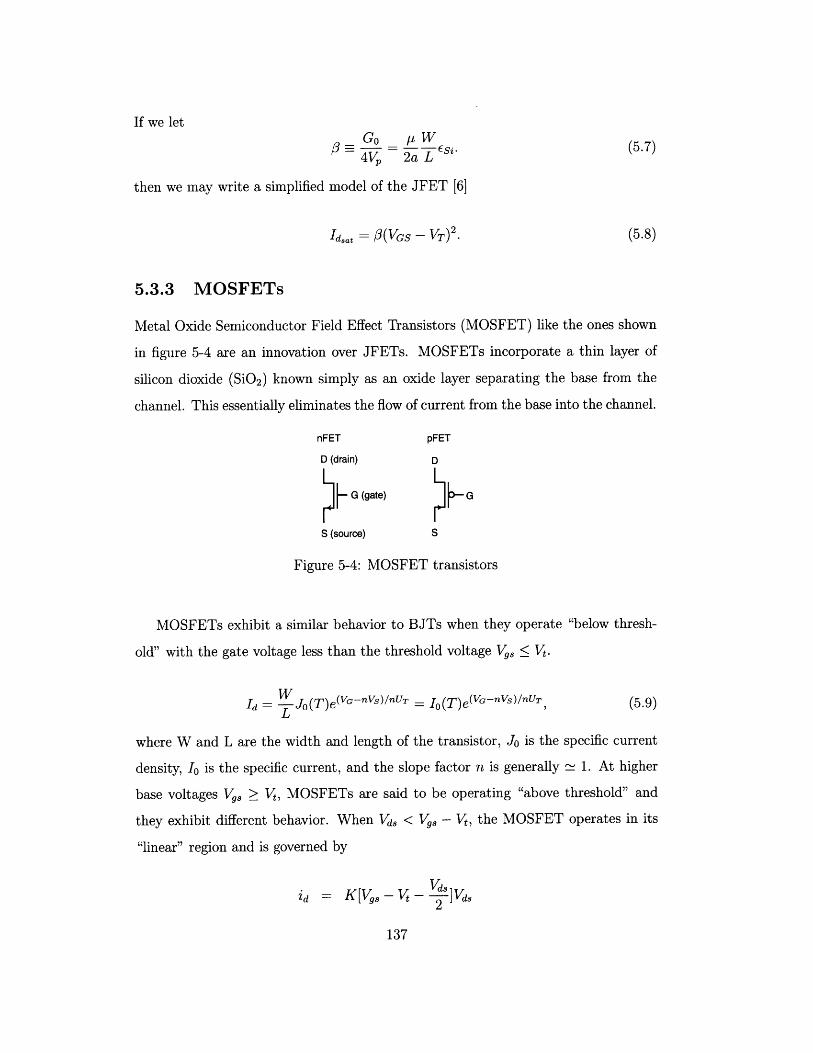
If we let_ Go _ p W (5.7)
- 4V, 2aL si-
then we may write a simplified model of the JFET [6]
Id=at =(VGS - VT) 2 . (5.8)
5.3.3 MOSFETs
Metal Oxide Semiconductor Field Effect Transistors (MOSFET) like the ones shown
in figure 5-4 are an innovation over JFETs. MOSFETs incorporate a thin layer of
silicon dioxide (SiO 2 ) known simply as an oxide layer separating the base from the
channel. This essentially eliminates the flow of current from the base into the channel.
nFET pFET
D (drain) D
G (gate) G
S (source) S
Figure 5-4: MOSFET transistors
MOSFETs exhibit a similar behavior to BJTs when they operate "below thresh-
old" with the gate voltage less than the threshold voltage V, < Vt.
Is = WLJo(T) e(VG-nVs)/nUT = I0(T)e(VG-nVS)/nUT, (59)L
where W and L are the width and length of the transistor, Jo is the specific current
density, 1o is the specific current, and the slope factor n is generally ~ 1. At higher
base voltages Vg, ;> V, MOSFETs are said to be operating "above threshold" and
they exhibit different behavior. When V, < V, - Vt, the MOSFET operates in its
"linear" region and is governed by
Vdid = K[Vs - Vt - pVdI
137
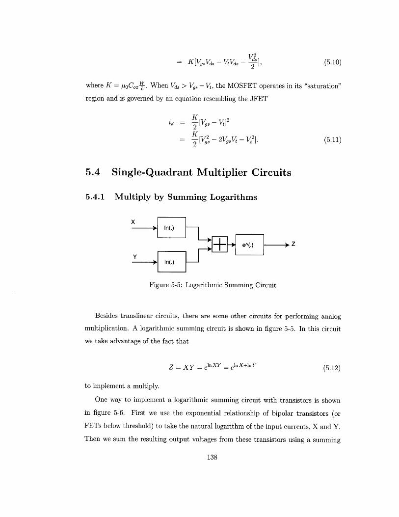
V2= K[VsVd 8 - V Vds- ], (5.10)
where K = po COX.,L!. When Vds > V, - Vt, the MOSFET operates in its "saturation"
region and is governed by an equation resembling the JFET
Kis = -[V t-]2
Kd [V2 V 2].
- [V2- 2VV tV2 ]. (5.11)
5.4 Single-Quadrant Multiplier Circuits
5.4.1 Multiply by Summing Logarithms
xIn(.
->e^(.) Z
Y
Figure 5-5: Logarithmic Summing Circuit
Besides translinear circuits, there are some other circuits for performing analog
multiplication. A logarithmic summing circuit is shown in figure 5-5. In this circuit
we take advantage of the fact that
Z = XY = el XY = eIn X+n (5.12)
to implement a multiply.
One way to implement a logarithmic summing circuit with transistors is shown
in figure 5-6. First we use the exponential relationship of bipolar transistors (or
FETs below threshold) to take the natural logarithm of the input currents, X and Y.
Then we sum the resulting output voltages from these transistors using a summing
138
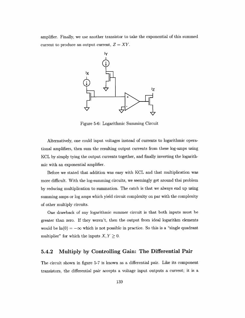
amplifier. Finally, we use another transistor to take the exponential of this summed
current to produce an output current, Z = XY.
ly
Ix
IZ
Figure 5-6: Logarithmic Summing Circuit
Alternatively, one could input voltages instead of currents to logarithmic opera-
tional amplifiers, then sum the resulting output currents from these log-amps using
KCL by simply tying the output currents together, and finally inverting the logarith-
mic with an exponential amplifier.
Before we stated that addition was easy with KCL and that multiplication was
more difficult. With the log-summing circuits, we seemingly get around thsi problem
by reducing multiplication to summation. The catch is that we always end up using
summing amps or log amps which yield circuit complexity on par with the complexity
of other multiply circuits.
One drawback of any logarithmic summer circuit is that both inputs must be
greater than zero. If they weren't, then the output from ideal logarithm elements
would be ln(O) = -oc which is not possible in practice. So this is a "single quadrant
multiplier" for which the inputs X, Y > 0.
5.4.2 Multiply by Controlling Gain: The Differential Pair
The circuit shown in figure 5-7 is known as a differential pair. Like its component
transistors, the differential pair accepts a voltage input outputs a current; it is a
139
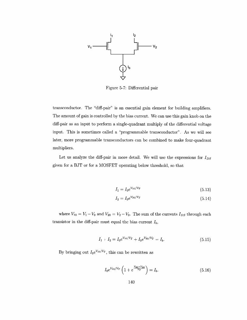
11 12
V1 V2
Figure 5-7: Differential pair
transconductor. The "diff-pair" is an essential gain element for building amplifiers.
The amount of gain is controlled by the bias current. We can use this gain knob on the
diff-pair as an input to perform a single-quadrant multiply of the differential voltage
input. This is sometimes called a "programmable transconductor". As we will see
later, more programmable transconductors can be combined to make four-quadrant
multipliers.
Let us analyze the diff-pair in more detail. We will use the expressions for IDS
given for a BJT or for a MOSFET operating below threshold, so that
I1 = IOeV'O/v (5.13)
12 = IoeV2o/VT (5.14)
where V10 = V1 - V and V20 = V2 - V. The sum of the currents IDS through each
transistor in the diff-pair must equal the bias current Ib,
1 + 12 = IoeVo/v + Ioev2o/vT =b. (5.15)
By bringing out IoeVlo/v, this can be rewritten as
Ioeo/VT 1 + e VT )= Ib. (5.16)
140
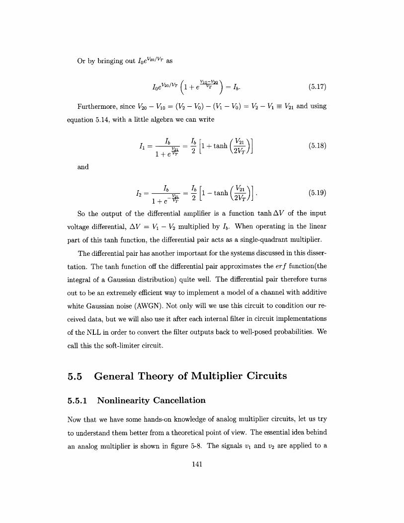
Or by bringing out IoeV2o/VT as
I V 2 0 / V Tv 1 0 - v 2 0 )IoeVo/V 1 + eV vr = Ib. (5.17)
Furthermore, since V2o - Vio = (V2 - Vo) - (V - V) = V2 - V V21 and using
equation 5.14, with a little algebra we can write
I1 - -i- + tanh V21 (5.18)1 + e vT 2 . 2VT
and
A2 Ab _ [~a V21112 - -[-1 - tanh .2Vr) (5.19)
1+e vr
So the output of the differential amplifier is a function tanh AV of the input
voltage differential, AV = V1 - V2 multiplied by I. When operating in the linear
part of this tanh function, the differential pair acts as a single-quadrant multiplier.
The differential pair has another important for the systems discussed in this disser-
tation. The tanh function off the differential pair approximates the erf function(the
integral of a Gaussian distribution) quite well. The differential pair therefore turns
out to be an extremely efficient way to implement a model of a channel with additive
white Gaussian noise (AWGN). Not only will we use this circuit to condition our re-
ceived data, but we will also use it after each internal filter in circuit implementations
of the NLL in order to convert the filter outputs back to well-posed probabilities. We
call this the soft-limiter circuit.
5.5 General Theory of Multiplier Circuits
5.5.1 Nonlinearity Cancellation
Now that we have some hands-on knowledge of analog multiplier circuits, let us try
to understand them better from a theoretical point of view. The essential idea behind
an analog multiplier is shown in figure 5-8. The signals vi and v2 are applied to a
141
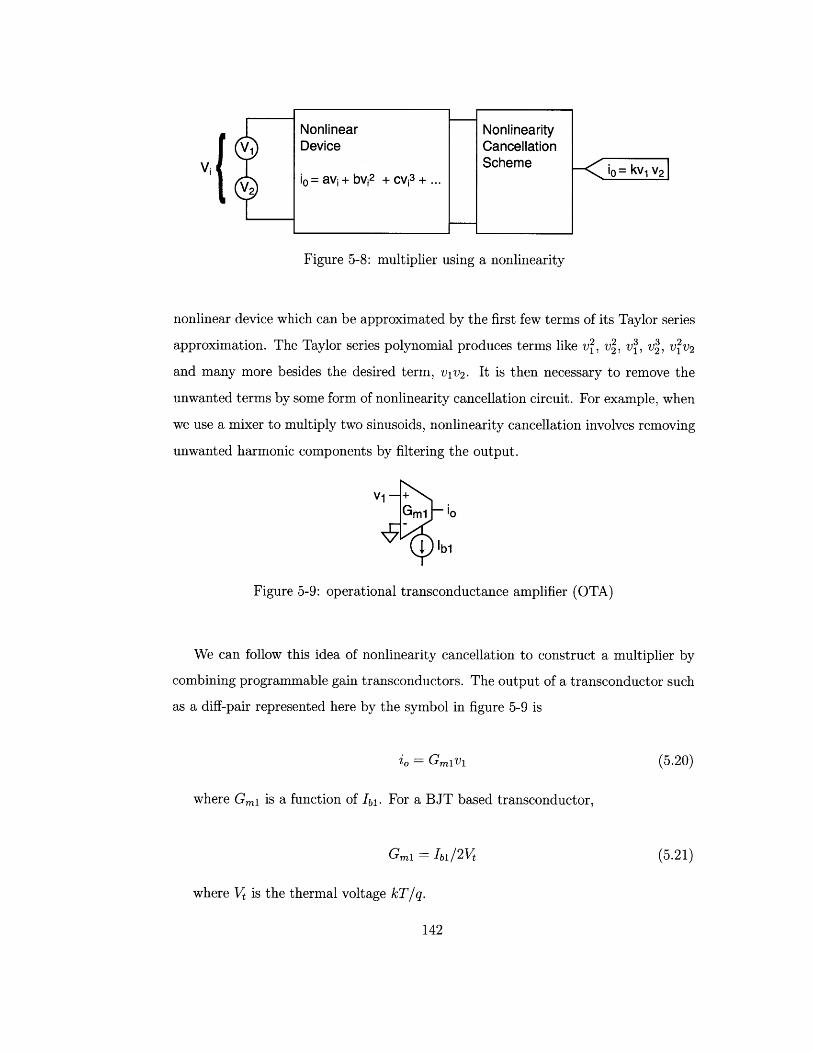
Figure 5-8: multiplier using a nonlinearity
nonlinear device which can be approximated by the first few terms of its Taylor series
approximation. The Taylor series polynomial produces terms like vi, o , v , v , v v2
and many more besides the desired term, v1v2. It is then necessary to remove the
unwanted terms by some form of nonlinearity cancellation circuit. For example, when
we use a mixer to multiply two sinusoids, nonlinearity cancellation involves removing
unwanted harmonic components by filtering the output.
Figure 5-9: operational transconductance amplifier (OTA)
We can follow this idea of nonlinearity cancellation to construct a multiplier by
combining programmable gain transconductors. The output of a transconductor such
as a diff-pair represented here by the symbol in figure 5-9 is
io = Gmivi (5.20)
where Gmi is a function of Ibl. For a BJT based transconductor,
where Vt is the thermal voltage kT/q.
142
Gmi = Ibl/2Vt (5.21)
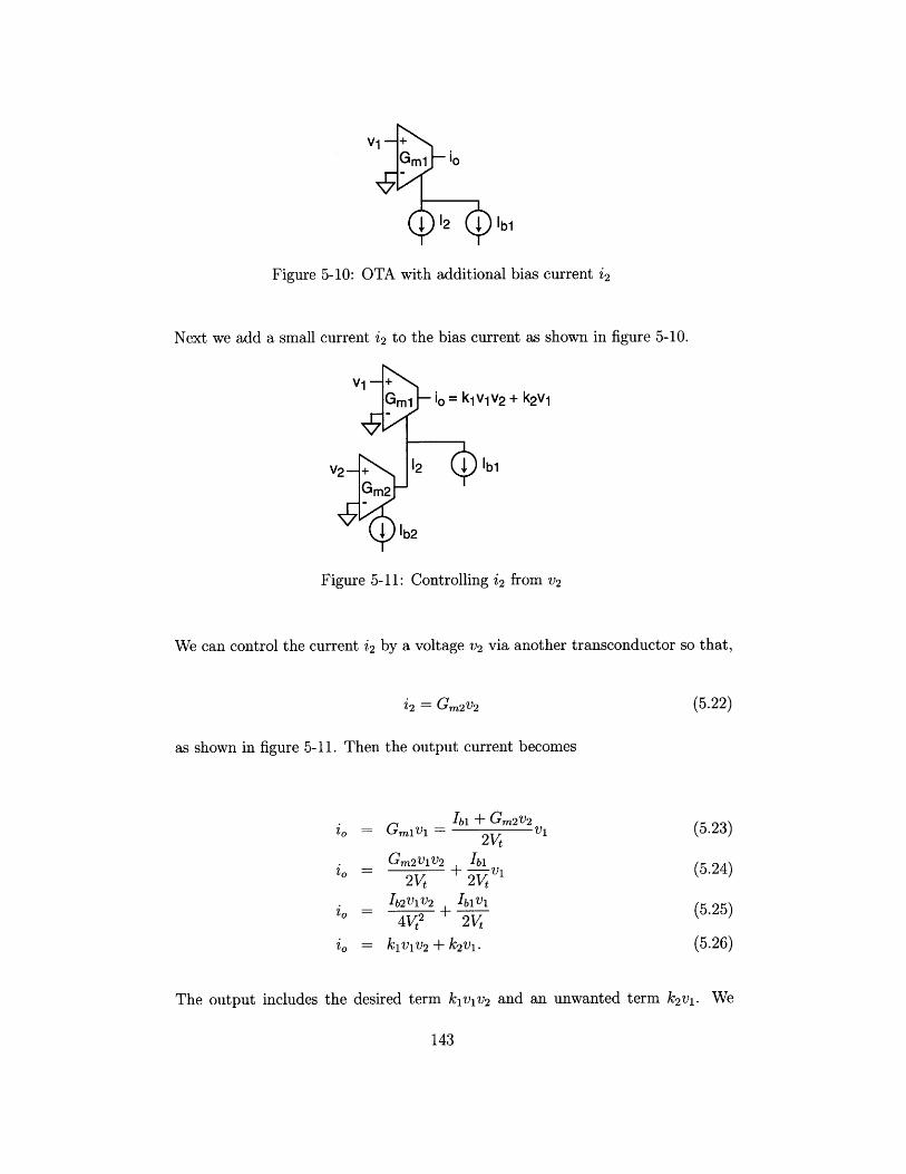
(4 12 (4 lb1Figure 5-10: OTA with additional bias current i2
Next we add a small current i2 to the bias current as shown in figure 5-10.
io = k1v1v2 + k2v1
Figure 5-11: Controlling i2 from v2
We can control the current i2 by a voltage v2 via another transconductor so that,
(5.22)i2= Gm2V2
as shown in figure 5-11. Then the output current becomes
Ibl+Gm2V22= Gmiv i 2 Vi
Gm2V1V2 Ibl2o+ 2V20 - t 2 2 2
Ib2V1V242 + Ib112
io = k1v1v2 +k 2v1.
The output includes the desired term kiv 1 v2 and an unwanted term k2 V1. We
143
(5.23)
(5.24)
(5.25)
(5.26)
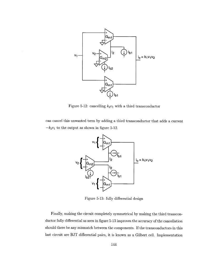
io = k1v1v2
Figure 5-12: cancelling k2vi with a third transconductor
can cancel this unwanted term by adding a third transconductor that adds a current
-k 2v1 to the output as shown in figure 5-12.
io = k1v1v 2
Figure 5-13: fully differential design
Finally, making the circuit completely symmetrical by making the third transcon-
ductor fully differential as seen in figure 5-13 improves the accuracy of the cancellation
should there be any mismatch between the components. If the transconductors in this
last circuit are BJT differential pairs, it is known as a Gilbert cell. Implementation
144
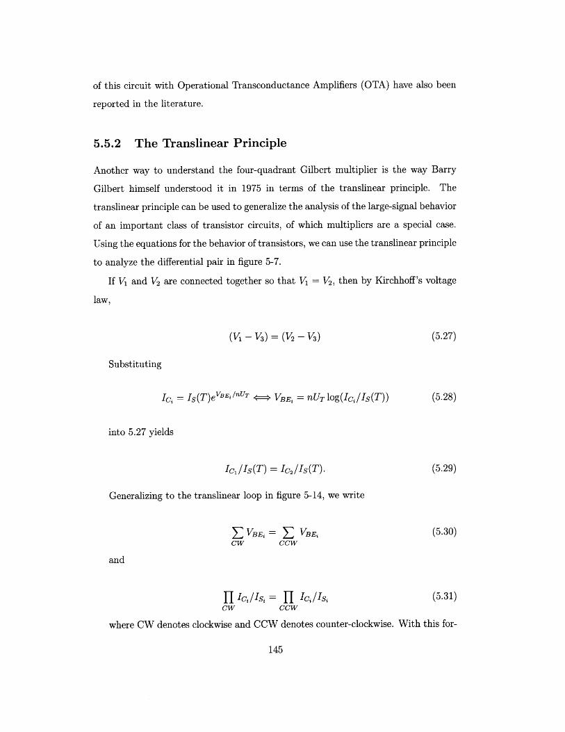
of this circuit with Operational Transconductance Amplifiers (OTA) have also been
reported in the literature.
5.5.2 The Translinear Principle
Another way to understand the four-quadrant Gilbert multiplier is the way Barry
Gilbert himself understood it in 1975 in terms of the translinear principle. The
translinear principle can be used to generalize the analysis of the large-signal behavior
of an important class of transistor circuits, of which multipliers are a special case.
Using the equations for the behavior of transistors, we can use the translinear principle
to analyze the differential pair in figure 5-7.
If V and V2 are connected together so that V = V2, then by Kirchhoff's voltage
law,
(V1 - V3) = (V2 -V 3) (5.27)
Substituting
Ic. = Is(T)eVBEi/nUT 4 VBE= nUT log(1c/Is(T)) (5.28)
into 5.27 yields
I 1 /Is(T) = Ic 2 /Is(T). (5.29)
Generalizing to the translinear loop in figure 5-14, we write
E VBE, = E VBEj (5.30)CW CCW
and
7 Ic"/is, = 1 'c,/isi (5.31)CW CCW
where CW denotes clockwise and CCW denotes counter-clockwise. With this for-
145
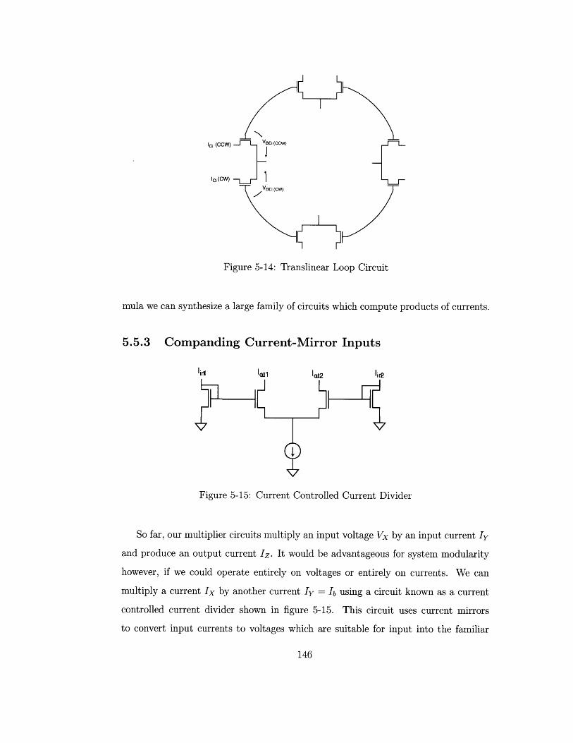
Ici (CCW)
Ici (CW) -1 rT VBEi (CW)
Figure 5-14: Translinear Loop Circuit
mula we can synthesize a large family of circuits which compute products of currents.
5.5.3 Companding Current-Mirror Inputs
Figure 5-15: Current Controlled Current Divider
So far, our multiplier circuits multiply an input voltage Vx by an input current ly
and produce an output current 1z. It would be advantageous for system modularity
however, if we could operate entirely on voltages or entirely on currents. We can
multiply a current Ix by another current Iy = lb using a circuit known as a current
controlled current divider shown in figure 5-15. This circuit uses current mirrors
to convert input currents to voltages which are suitable for input into the familiar
146
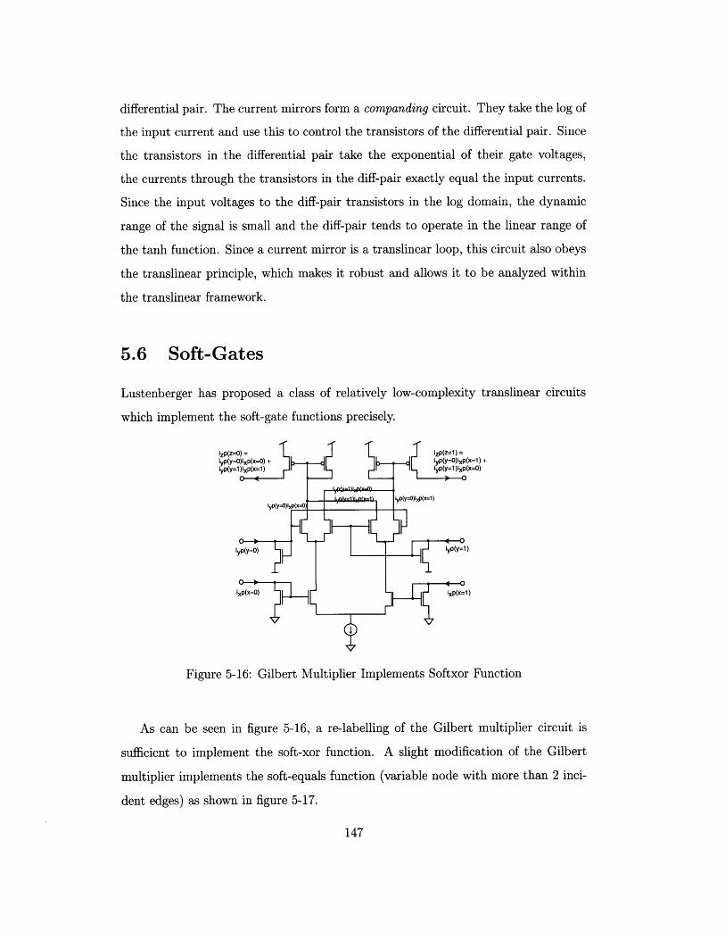
differential pair. The current mirrors form a companding circuit. They take the log of
the input current and use this to control the transistors of the differential pair. Since
the transistors in the differential pair take the exponential of their gate voltages,
the currents through the transistors in the diff-pair exactly equal the input currents.
Since the input voltages to the diff-pair transistors in the log domain, the dynamic
range of the signal is small and the diff-pair tends to operate in the linear range of
the tanh function. Since a current mirror is a translinear loop, this circuit also obeys
the translinear principle, which makes it robust and allows it to be analyzed within
the translinear framework.
5.6 Soft-Gates
Lustenberger has proposed a class of relatively low-complexity translinear circuits
which implement the soft-gate functions precisely.
IYP(yO)IXP(X=O) + Iy~0 PX=1) +IyP(Yl )IxP(X=l) y(l)Px0
- - lyp(y=0)1xp(x=1)IyP(y=O)IxP(x=O)
IYp(y=O) IYP(y=1)
Ixp(XO) Ixp(X1)
Figure 5-16: Gilbert Multiplier Implements Softxor Function
As can be seen in figure 5-16, a re-labelling of the Gilbert multiplier circuit is
sufficient to implement the soft-xor function. A slight modification of the Gilbert
multiplier implements the soft-equals function (variable node with more than 2 inci-
dent edges) as shown in figure 5-17.
147
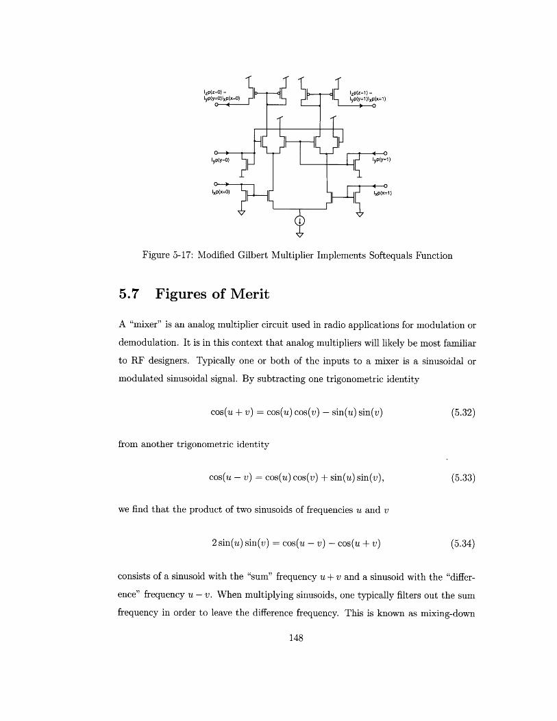
Figure 5-17: Modified Gilbert Multiplier Implements Softequals Function
5.7 Figures of Merit
A "mixer" is an analog multiplier circuit used in radio applications for modulation or
demodulation. It is in this context that analog multipliers will likely be most familiar
to RF designers. Typically one or both of the inputs to a mixer is a sinusoidal or
modulated sinusoidal signal. By subtracting one trigonometric identity
cos(u + v) = cos(u) cos(v) - sin(u) sin(v) (5.32)
from another trigonometric identity
cos(u - v) = cos(u) cos(v) + sin(u) sin(v), (5.33)
we find that the product of two sinusoids of frequencies u and v
2 sin(u) sin(v) = cos(u - v) - cos(u + v) (5.34)
consists of a sinusoid with the "sum" frequency u + v and a sinusoid with the "differ-
ence" frequency u - v. When multiplying sinusoids, one typically filters out the sum
frequency in order to leave the difference frequency. This is known as mixing-down
148
or down-conversion and is the essential building block in a heterodyne radio receiver.
We are using mixer-type circuits, but are using them to operate on completely
different signals. Instead of sinusoidal signals, we have analog probability levels. The
question is how well can mixer-type circuits perform this function?
The merit of a mixer is evaluated according to its "linearity", port-to-port isola-
tion, gain, noise figure, and dynamic range [54]. Attenuation or conversion loss and
port-to-port isolation are generally measured in dBm = log(signalpower/lmW) with
a 50Q load. Port-to-port isolation will effect our resolution to some degree, but it
will be much less important for us than it is in sinusoidally based RF demodulation.
This will be described in greater detail when we discuss the soft-MUX, but the basic
idea is that leakage signals don't tend to have as drastic impact on soft-decoding as
it does on RF down-conversion. In any event, the best isolation is achieved by PIN
diodes which are used as analog switches and offer approximately 70dBm of isolation.
Typical "Gilbert cell" active mixers offer on the order of 30dB of isolation.
Linearity in this context means how accurately the actual mixer function adheres
to an ideal mathematical multiplication. It is an open and interesting research ques-
tion to fully characterize how linearity of the multiplies will affect the sum-product
algorithm, but we know from preliminary simulations that the affect will not be
catastrophic. Linearity should therefore be de-emphasized as a design constraint.
In practice, this means we can push our circuits to operate outside of their linear
range and therefore obtain a larger dynamic range from the same circuit for the same
amount of power.
The sum-product algorithm is guaranteed to reach a maximum-likelihood estimate
on a graph without cycles. By turning up the gain on a multiply in the sum-product
algorithm it is actually possible to speed up the sum-product algorithm, while sac-
rificing the guarantee that the algorithm will converge to the maximum-likelihood
estimate. Since we have already sacrificed this guarantee in graphs with cycles, we
might even desire non-ideal multipliers to get quick and dirty estimates. If the actual
multiplier gives a function which is steeper than a "linear" multiply in the middle
range and then less steep at the edges, this may effectively schedule the annealing
149
process for the sum-product algorithm so that it goes faster in the beginning and
then slows down as it refines its answers at the end. This may be a good thing to do
in high SNR environments or in relatively easy searches where hasty early decisions
are unlikely to freeze the answer irrevocably into a bad region of the search space.
Passive mixers have attenuation and depend on post-amplification for their gain.
We are interested in active mixers which tend to have gain between 0 and 5. 8 would
be a lot of gain for a mixer. For our purposes, we are free to scale our signals in
any way we please so that we do not need gain from our mixer circuits, although we
would prefer not to have attenuation. We simply take the ratio of dynamic range and
the noise to obtain the resolution.
A typical mixer has 5-8 bits of resolution. This is pretty useful for decoding. In
soft decoding we would like our resolution to be at least 2 bits and would prefer
as much as 8 bits of resolution. By way of comparison, demodulation of sinusoids
by digital signal processing uses 12 or 14 bits of resolution and CD quality audio
utilizes 16 bits of resolution. The best analog-to-digital converters today offer 24 bits
of resolution. Mixer circuits, like all all analog circuits, tend to be specified with
dynamic range and a noise figure in SNR and not in bits of resolution. The table
below converts some common values of resolution (in bits) to SNR (power)
SNR = 20 log ( (5.35)Ns p
where PS is the signal power and PN is the noise power.
150
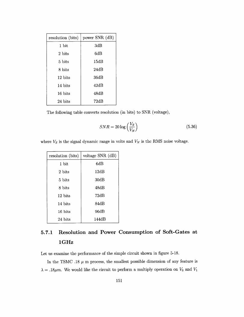
The following table converts resolution (in bits) to SNR (voltage),
SNR = 20 log ( Vs (5.36)
where Vs is the signal dynamic range in volts and VN is the RMS noise voltage.
5.7.1 Resolution
1GHz
and Power Consumption of Soft-Gates at
Let us examine the performance of the simple circuit shown in figure 5-18.
In the TSMC .18 p m process, the smallest possible dimension of any feature is
A = .18pm. We would like the circuit to perform a multiply operation on V and V
151
resolution (bits) power SNR (dB)
1 bit 3dB
2 bits 6dB
5 bits 15dB
8 bits 24dB
12 bits 36dB
14 bits 42dB
16 bits 48dB
24 bits 72dB
resolution (bits) voltage SNR (dB)
1 bit 6dB
2 bits 12dB
5 bits 30dB
8 bits 48dB
12 bits 72dB
14 bits 84dB
16 bits 96dB
24 bits 144dB
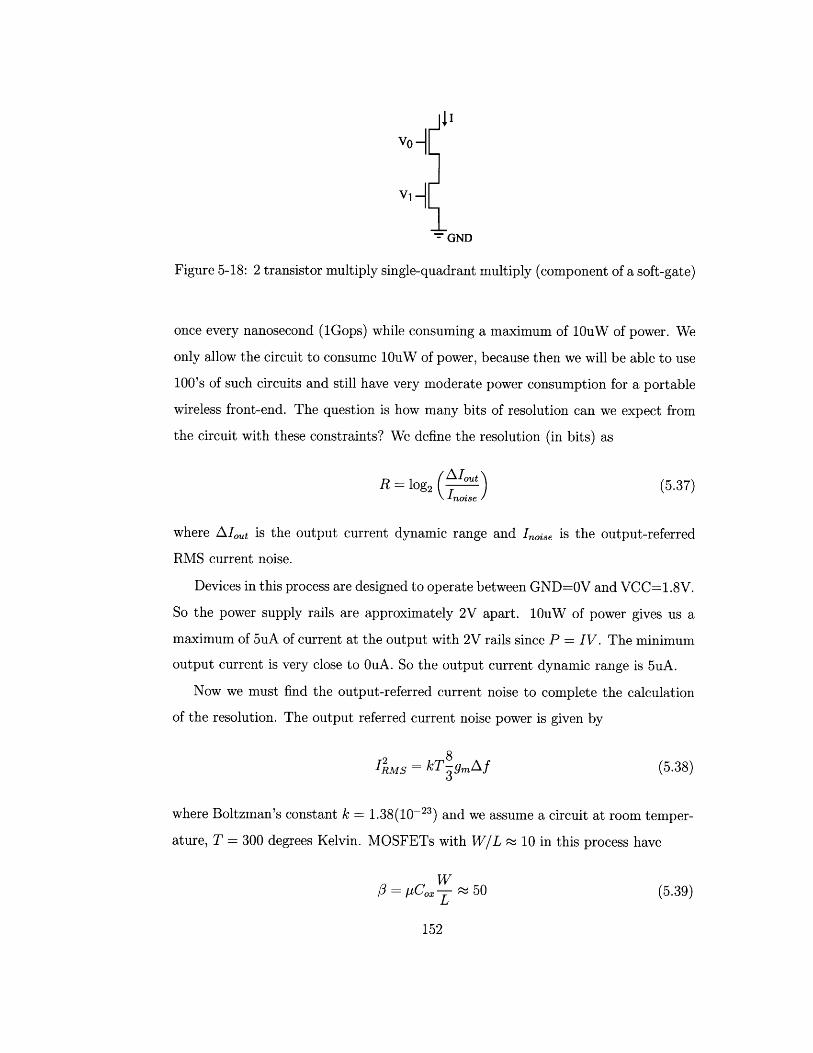
'I'VO]
Vi
- GND
Figure 5-18: 2 transistor multiply single-quadrant multiply (component of a soft-gate)
once every nanosecond (IGops) while consuming a maximum of 10uW of power. We
only allow the circuit to consume 10uW of power, because then we will be able to use
100's of such circuits and still have very moderate power consumption for a portable
wireless front-end. The question is how many bits of resolution can we expect from
the circuit with these constraints? We define the resolution (in bits) as
R log 2 ( (5.37)
where AzIt is the output current dynamic range and Inoise is the output-referred
RMS current noise.
Devices in this process are designed to operate between GND=OV and VCC=1.8V.
So the power supply rails are approximately 2V apart. 10uW of power gives us a
maximum of 5uA of current at the output with 2V rails since P = IV. The minimum
output current is very close to OuA. So the output current dynamic range is 5uA.
Now we must find the output-referred current noise to complete the calculation
of the resolution. The output referred current noise power is given by
8I s = kT gm f (5.38)3
where Boltzman's constant k = 1.38(10-23) and we assume a circuit at room temper-
ature, T = 300 degrees Kelvin. MOSFETs with W/L ~ 10 in this process have
WO=pC - ~ 50 (5.39)
L
152
We can therefore calculate the transconductance gm ~ 400uS from
21=m = -
= V2. (5.40)
We are interested in a soft-gate that operates over a bandwidth of 1GHz so that
Af = 1O9Hz. We can now calculate IRMS ~ 10-15 and therefore the output-referred
current noise is IRMS ~ 3.3(10- )A. The resolution is therefore approximately R
log2(5uA/.033uA) = log 2(150) ~ 7 bits.
We might wonder what range of voltages we should use to drive this circuit at
the input in order to achieve the above performance. For a transistor in this process,
Cox .02pA/V 2. With W/L = 2um/.18um ~ 10, the gate capacitance is about
C,= (2/3)WLCOx ~ 4fF. Assuming a sinusoidal signal
V = Vsin(27rfe)dV-p = V27rfc cos(27rfc)dtdV
max dt = V,27rfcIcos(2-fc)-, (5.41)
and substituting into the definition of capacitance I= C L, we find that
CV, = -27fe ~~ 200mV (5.42)
I
where I=5uA, C=4fF, and fc = 1GHz. So v.= 400mV.
Further simulation is needed to verify and extend these back-of-the-envelope cal-
culations, but it seems promising that MOSFET soft-gates in non-heroic processes
can operate on reasonably high-frequency signals.
153

154
-- -- .s;.1--;.,;-..s...:1...:-.--s-.:......,..s --. ..... .....:. :--::--...''-''---t: ''.---='- n'+',:fC.''"4!k--r'WhiG-.:---a:'NT'en n .'.+:-*4-~'3-&- -
Chapter 6
The Sum Product Algorithm in
Continuous-Time
6.1 Differential Message Passing
Annealing is what happens when we try to cool a material so that it forms a per-
fect crystal without "discontinuities". At the atomic level, a perfect crystal would
be spatially invariant; Every part of the crystal would be a perfect copy of every
other part of the crystal. This perfectly symmetrical state, although it is the lowest
possible energy state of a crystal, is actually quite difficult to achieve, because differ-
ent parts of the crystal often grow from unconnected "seeds". Crystal will start to
form independently at different places in a liquid that is beginning to freeze, and by
time the entire material is frozen, there may be several different crystal orientations
present. The frozen material tends to break more easily along the discontinuities
between neighboring regions of differing orientation. To avoid this problem, Japanese
Samurai swords were painstakingly annealed through a process of successive heating
and cooling. On each heating stage, the metal crystal would be melted a bit, allowing
regions of the crystal that might have been misaligned with one another to work out
some of their "kinks." Then the metal is cooled again and the process is repeated.
Annealing works because adjacent atoms in the material would prefer to be in
alignment than randomly oriented to one another. This preference can be modelled
155
by an energy function over the possible alignments or states of the two atoms. In this
way the total energy of a crystalline material is composed of a very large number of
pairwise energy functions over pairs of atoms. As a crystal is annealed, the atoms are
all acting on each other in continuous-time, trying to lower the energy of all of the
pairs in which they participate.
Physicists model each atom in an annealing crystal as having a probability dis-
tribution over its possible states. The energy function, when normalized, is then
really a joint probability distribution. Such a model should by now appear rather
familiar. Physicists call such models a spin-glass, and research on spin-glasses was an
important ancestor of probabilistic message passing algorithms.
When a crystal is annealed, the atoms in the material are in effect performing a
constraint satisfaction computation. The converse is also true - constraint satisfaction
problems in computer science bear a deep resemblance to spin-glass annealing. All
the sum-product algorithm is really doing is performing pairwise interactions between
adjacent states in an attempt to settle to a mutually compatible solution. Just like
annealing, probabilistic message passing algorithms ought properly to be implemented
as a continuous-time parallel process.
Unfortunately, because discrete-time serial computers are generally the only ones
readily available to us, we adopt a discrete-time approximation to the continuous-
time process. Such a discrete-time approximation should have the property that
every message gets updated when there is enough new information available from
other messages to justify recomputing the message. One definition of "enough" could
be that a message is computed for an (outgoing) edge from a given node when all
of the other (incoming) edges to that node have new messages coming in. This idea
is the origin of the message passing schedule discussed in the last chapter. There is
no proof, however, that this schedule is guaranteed to find the same answer as the
continuous-time process would have. In fact, it will often diverge from the continuous-
time solution, producing wrong answers which are merely an artifact of the scheduling.
When this happens, we use damping.
156
6.1.1 Damping
Damping means that messages consist of a linear combination of the current calcu-
lated message and the last calculated message in the same direction on the same
edge,
Pt =apt + (1 - a)p-t-1. (6.1)
6.1.2 Von Neuman Stability Analysis of Finite Differences
Finite difference models of partial differential equations (PDE) have much in common
with probabilistic message passing algorithms on a Markov Random Field. In each
case we have a grid of states which update in time based on functions of their local
neighbors. And in both cases, we approximate continuous-time updates with discrete-
time updates. Of course there is an important difference; In a finite difference model
of a PDE, the functions impose constraints on the derivative of the solution, while in
probabilistic message passing, the constraints can be more general.
It is not yet understood under which conditions damping stabilizes discrete-time
probabilistic message passing so that it converges to the continuous-time solution.
There is, however, a suggestively similar procedure for stabilizing the discrete-time
(and discrete-space) finite difference model of a PDE. A Von Neumann stability anal-
ysis is a well-understood way to analyze the stability of a finite difference model of a
PDE.
Our finite difference model in one dimension will consist of a row of states, u
indexed in space by j and in time by n. So at time n, a point in space on the solution
of the PDE is a real number, un. To perform the stability analysis, we linearize the
PDE (if it is not already) and observe the growth of sinusoidal modes
n = A(k)neikix (6.2)
in the system, where A(k) gives an exponentially growing amplitude in time for
157
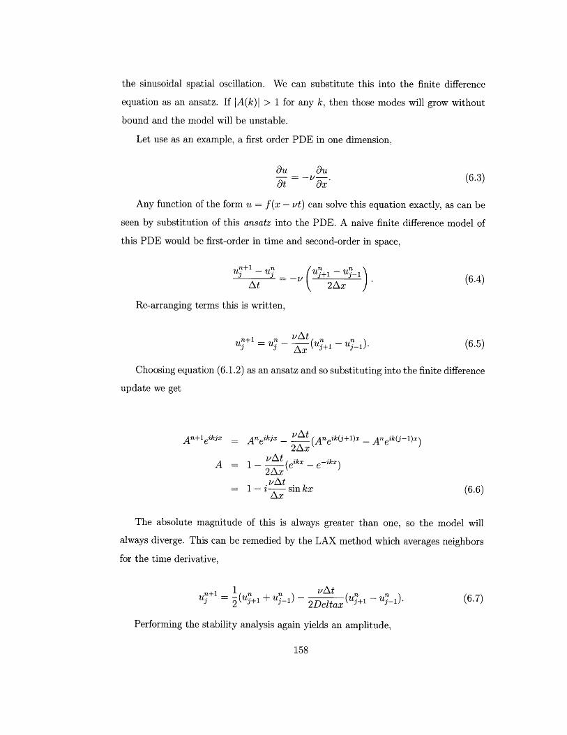
the sinusoidal spatial oscillation. We can substitute this into the finite difference
equation as an ansatz. If IA(k)| > 1 for any k, then those modes will grow without
bound and the model will be unstable.
Let use as an example, a first order PDE in one dimension,
au B9U= -V_ .(6.3)at ax
Any function of the form u f(x - vt) can solve this equation exactly, as can be
seen by substitution of this ansatz into the PDE. A naive finite difference model of
this PDE would be first-order in time and second-order in space,
Ujn+1 - Y nZ+ - "-1n+ j+~= -V .'1 -~ (6.4)At ( 2Ax
Re-arranging terms this is written,
U +1 = j- (Un+1 - U-). (6.5)
Choosing equation (6.1.2) as an ansatz and so substituting into the finite difference
update we get
An+1eikjx = Aneikix - V (A eik(j+l)x - A eik(3-1)x)2Ax
A = 1- VAt _ikx ikx2AxvAt
1- i sinkx (6.6)Ax
The absolute magnitude of this is always greater than one, so the model will
always diverge. This can be remedied by the LAX method which averages neighbors
for the time derivative,
Uni-i1 n j) VAt -(n U )
a,+1 = (uZ+1 +uj71 ) -2Deltax (U+1 - 'u- 1 ). (6.7)
Performing the stability analysis again yields an amplitude,
158
v At.A = coskx - sin kx (6.8)
Ax
For the model to be stable, we require the magnitude of this complex amplitude
to always be less than 1 so that
/vAt 2AI' = cos2 kx + y ) sin 2 kx ; 1 (6.9)
(Ax
which is true under the condition that
IviAt < 1. (6.10)Ax
This is the Courant-Friedrichs-Levy stability criterion, which essentially says that
"the velocity at which information propagates in the numerical algorithm Ax/At,
must be faster than the velocity of the solution v... Otherwise there will be a numerical
"boom" as the real solution tries to out-run the rate at which the numerical solution
can advance [15]."
Damping in probabilistic message passing solves the same problem that the LAX
method solved in our finite difference model. If the true continuous-time annealing
process is trying to out-run the flow of information by message passing updates,
then the states need to change slower over more message updates. We can update
messages more slowly by averaging a message update with previous messages on the
same edge, ie. damping. It still remains for us to find an analogous bound to the
Courant-Friedrichs-Levy stability criterion for sum product which would tell us how
much and what kind of damping is enough to ensure stability and convergence of the
discrete-time model to the continuous-time solution. It is likely for example, that
for many inhomogeneous graphs, different amounts of damping could be tolerated at
different places in the graph.
159
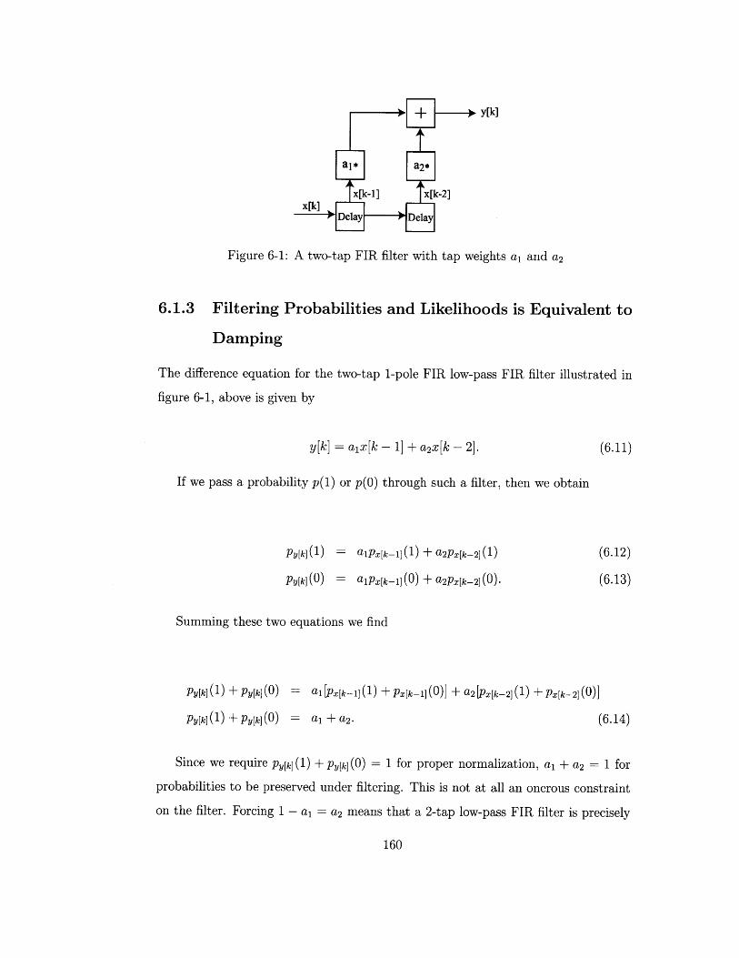
y[k]
Figure 6-1: A two-tap FIR filter with tap weights a1 and a 2
6.1.3 Filtering Probabilities and Likelihoods is Equivalent to
Damping
The difference equation for the two-tap 1-pole FIR low-pass FIR filter illustrated in
figure 6-1, above is given by
y[k] = aix[k - 1] + a2 x[k - 2]. (6.11)
If we pass a probability p(l) or p(O) through such a filter, then we obtain
py[k](1) alpx[k-1](1) + a2px[k-2](1) (6-12)
Py[k](0) alpz[k-1](0) ± a2pz[k-2](O)- (6.13)
Summing these two equations we find
Py[k](1) +Py[k](0) = al[px[k1(1) +Px[k-1](0)] + a2[Px[k-2](1) +px[k-2](0)]
Py[k](1) + py[k](0) = ai +a 2. (6.14)
Since we require Py[k] (1) + Py[k] (0) = 1 for proper normalization, a1 + a 2 = 1 for
probabilities to be preserved under filtering. This is not at all an onerous constraint
on the filter. Forcing 1 - ai = a 2 means that a 2-tap low-pass FIR filter is precisely
160
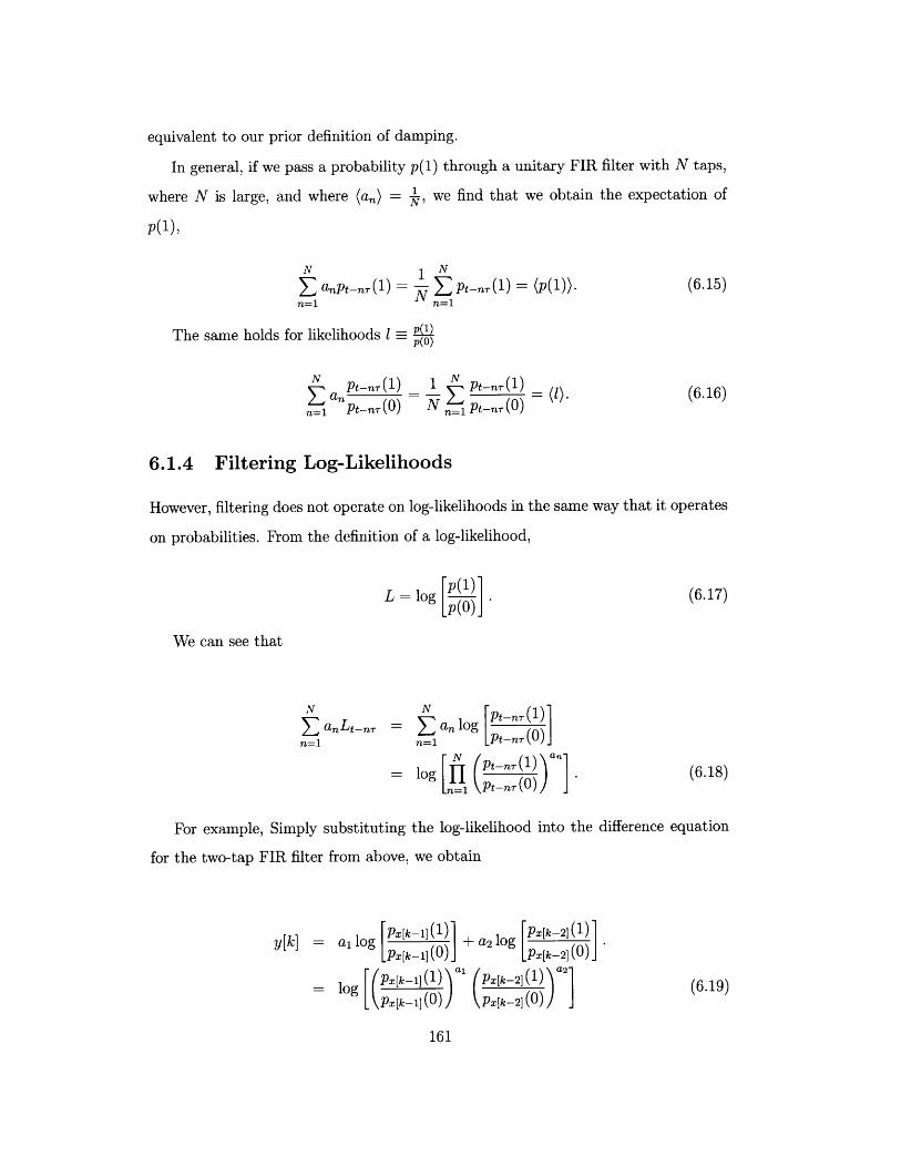
equivalent to our prior definition of damping.
In general, if we pass a probability p(l) through a unitary FIR filter with N taps,
where N is large, and where (an) = , we find that we obtain the expectation of
n= 1(6.15)anpt-_r (1) = p _tr (1) = (p(1)).
Nn= 1
The same holds for likelihoods 1 = Pp(O)
N Pt-nr(i)Eann=1 Pt-nr (0)
N p__r(6.16)
6.1.4 Filtering Log-Likelihoods
However, filtering does not operate on log-likelihoods in the same way that it operates
on probabilities. From the definition of a log-likelihood,
L =log [PIp(0).I
(6.17)
We can see that
N
E anLt-nrn=1 n=1
a log [Pt-w- (log N (Pt - -(1)) an]
.I= Pt-nr- (0) .
(6.18)
For example, Simply substituting the log-likelihood into the difference equation
for the two-tap FIR filter from above, we obtain
= ai log -
Px [k-1|(0)1
= log -\Px[k-1 (0))
+ a2 log Px[k-2 (1)+ a 2 9 P x [k - 2|(0 ) .
a P k-2| (1) ) 2-
\Px k-2| (0) 1
y[k]
(6.19)
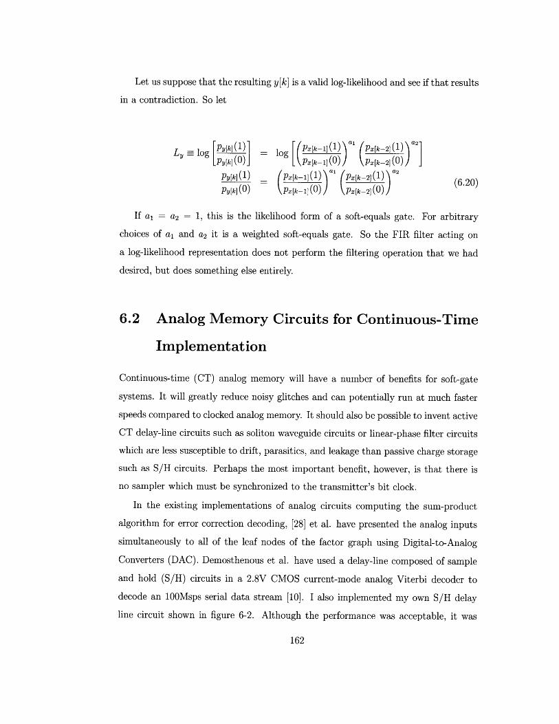
Let us suppose that the resulting y[k] is a valid log-likelihood and see if that results
in a contradiction. So let
L = log [Py[k] (1) log Px[k-1](1)) (P k-2 (1) a2][Py[k] (0 . _Px[k-1](0) Px[k-2] (0)).
Py[k] ( )Px~k-1] ( i) al -2] ( ) a2 ( 0/P ~ ( 1 ))0
Py[k](0) (\Px[k-1](0) )( Px[k-2](0) (
If ai = a2 = 1, this is the likelihood form of a soft-equals gate. For arbitrary
choices of ai and a2 it is a weighted soft-equals gate. So the FIR filter acting on
a log-likelihood representation does not perform the filtering operation that we had
desired, but does something else entirely.
6.2 Analog Memory Circuits for Continuous-Time
Implementation
Continuous-time (CT) analog memory will have a number of benefits for soft-gate
systems. It will greatly reduce noisy glitches and can potentially run at much faster
speeds compared to clocked analog memory. It should also be possible to invent active
CT delay-line circuits such as soliton waveguide circuits or linear-phase filter circuits
which are less susceptible to drift, parasitics, and leakage than passive charge storage
such as S/H circuits. Perhaps the most important benefit, however, is that there is
no sampler which must be synchronized to the transmitter's bit clock.
In the existing implementations of analog circuits computing the sum-product
algorithm for error correction decoding, [28] et al. have presented the analog inputs
simultaneously to all of the leaf nodes of the factor graph using Digital-to-Analog
Converters (DAC). Demosthenous et al. have used a delay-line composed of sample
and hold (S/H) circuits in a 2.8V CMOS current-mode analog Viterbi decoder to
decode an 10OMsps serial data stream [10]. I also implemented my own S/H delay
line circuit shown in figure 6-2. Although the performance was acceptable, it was
162
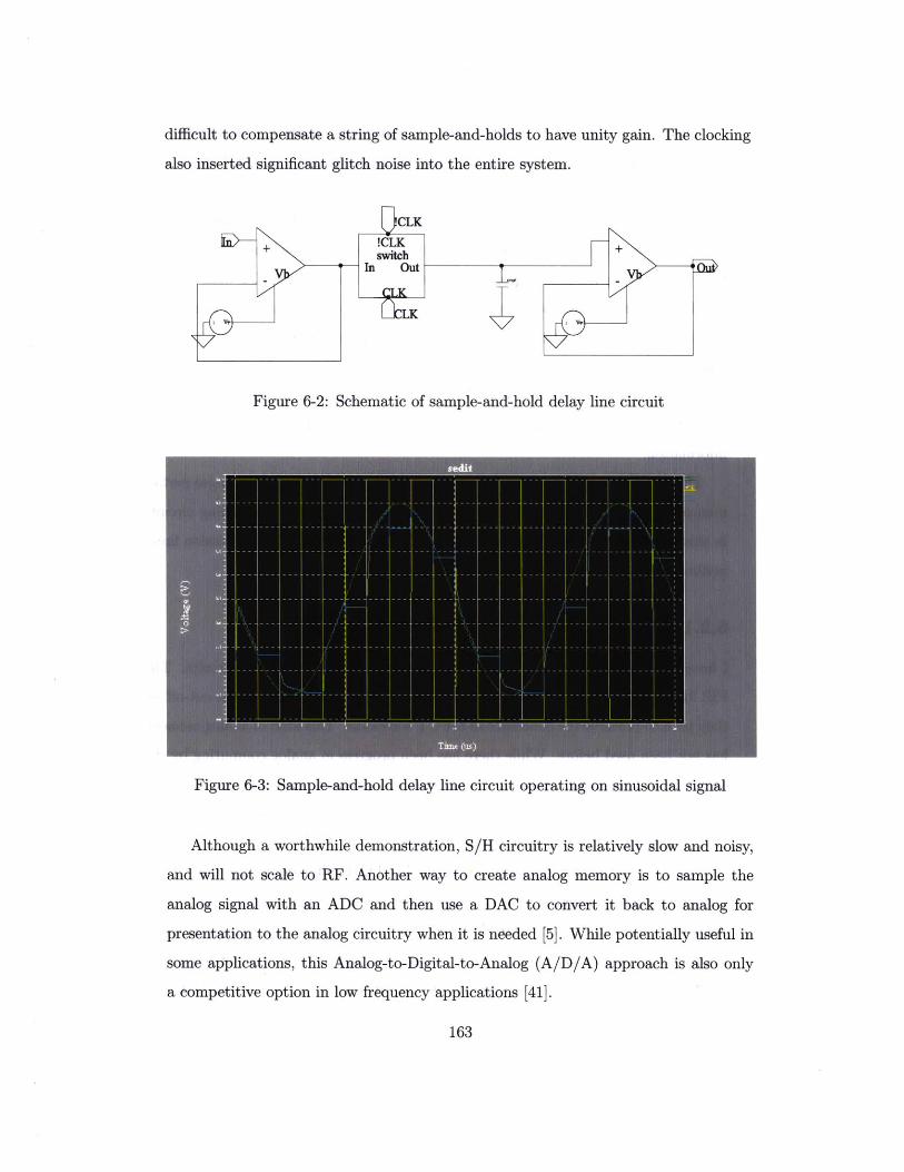
difficult to compensate a string of sample-and-holds to have unity gain. The clocking
also inserted significant glitch noise into the entire system.
Figure 6-2: Schematic of sample-and-hold delay line circuit
Figure 6-3: Sample-and-hold delay line circuit operating on sinusoidal signal
Although a worthwhile demonstration, S/H circuitry is relatively slow and noisy,
and will not scale to RF. Another way to create analog memory is to sample the
analog signal with an ADC and then use a DAC to convert it back to analog for
presentation to the analog circuitry when it is needed [5]. While potentially useful in
some applications, this Analog-to-Digital-to-Analog (A/D/A) approach is also only
a competitive option in low frequency applications [41].
163
There are a number of possible ways to implement analog CT delay-lines. In
this thesis I demonstrate a proof of principal by implementing analog CT delay with
linear-phase FIR low-pass filters. Unfortunately, linear phase low-pass filters are
likely to be too complex to be cost-effectively integrated. This is because by pre-
serving linear phase, the FIR filters are actually preserving much more information
than is absolutely necessary. It should be possible to build simpler CT delay circuits
which still preserve the analog amplitudes and perform appropriate smoothing with-
out the overhead of maintaining linear phase delay. A hint is offered by Carver Mead's
much simpler CT delay-line circuits which delay (digital) "neural" pulses. What is
needed are circuits which, like Mead's simple spike delay-lines, are less complex than
linear-phase FIR filters, but which preserve the (for us) crucial analog amplitude
information.
The engineering decisions for CT delay line circuits trade-off length, noise perfor-
mance, bandwidth, and dispersion. Future work will be directed at finding circuits
in this middle ground, perhaps drawing on integrated micro-strip transmission lines,
nonlinear transmission lines, or soliton waveguide circuits [46].
6.2.1 Active Low-Pass Filters
I have implemented CT analog delay-lines with FIR Chebychev filter circuits. The
FIR filters are designed to have linear phase delay over frequencies up to the cut-off, so
they tend to preserve the coherence of the CT waveform. This kind of analog memory
has not been used before. While there has been progress in analog computing by the
invention of translinear circuits to implement sum-product computations, storing a
baseband RF signal and presenting it to the decoder is a more open problem. We
have analog logic, now we need analog memory.
The system was first simulated using the MATLAB filter design toolbox. Then
the filter circuits schematic were designed using a filter design program from Filter
Solutions. Once the filters were designed, the entire system was simulated using
PSpice circuit simulator. Finally, it is a relatively straight-forward matter to convert
the Spice net-list schematic representation into an actual printed circuit board or
164
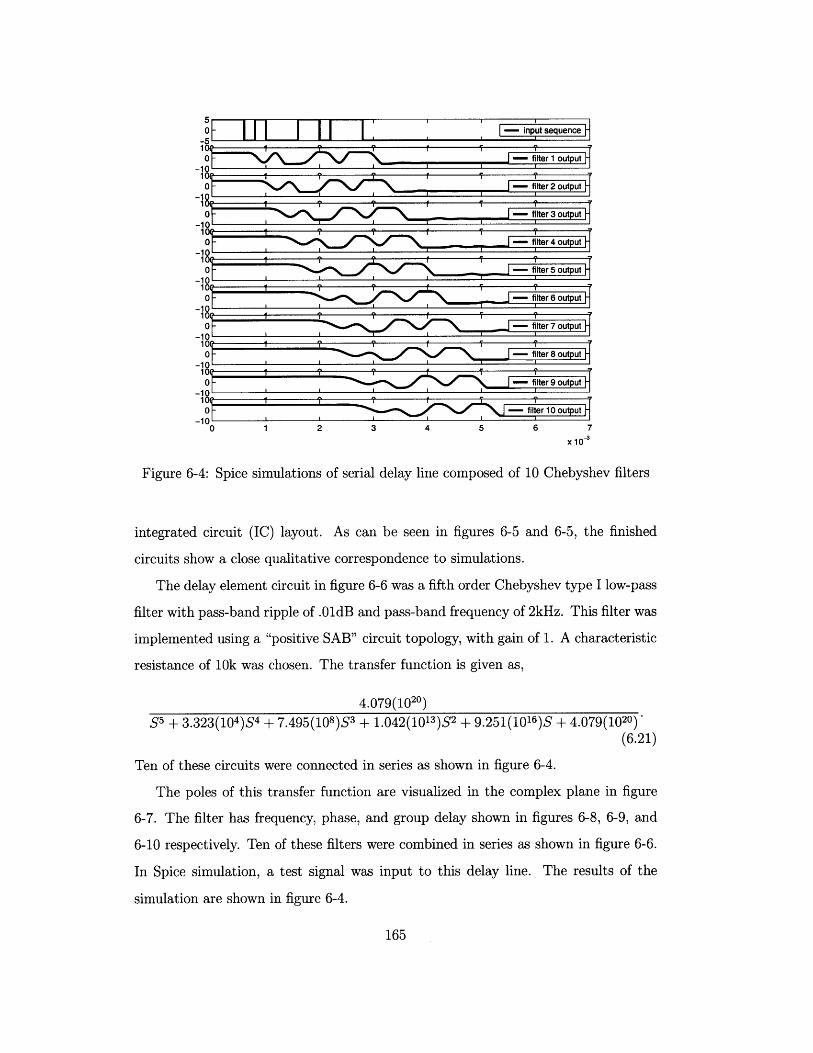
- - input sequence-5
o - filter 1 output
0 - filter 2 output10
0 -f iter output-10
0 - filter 4 output
-10
-101
0 -filter 6 output-10
10 1 fiter 7 output-10
1 0
10 - filter output-1010
-10~101?
10 - fle 0otu
-100 1 2 3 4 5 6 7
x 10
Figure 6-4: Spice simulations of serial delay line composed of 10 Chebyshev filters
integrated circuit (IC) layout. As can be seen in figures 6-5 and 6-5, the finished
circuits show a close qualitative correspondence to simulations.
The delay element circuit in figure 6-6 was a fifth order Chebyshev type I low-pass
filter with pass-band ripple of .01dB and pass-band frequency of 2kHz. This filter was
implemented using a "positive SAB" circuit topology, with gain of 1. A characteristic
resistance of 10k was chosen. The transfer function is given as,
4.079(1020)
S5 + 3.323(104)S4 + 7.495(108)S3 + 1.042(1013)S2 + 9.251(1016)S + 4.079(1020)(6.21)
Ten of these circuits were connected in series as shown in figure 6-4.
The poles of this transfer function are visualized in the complex plane in figure
6-7. The filter has frequency, phase, and group delay shown in figures 6-8, 6-9, and
6-10 respectively. Ten of these filters were combined in series as shown in figure 6-6.
In Spice simulation, a test signal was input to this delay line. The results of the
simulation are shown in figure 6-4.
165
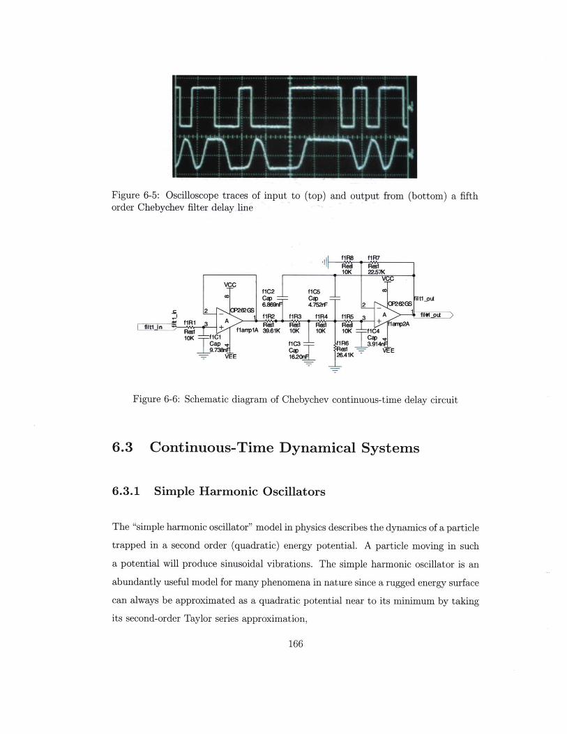
Figure 6-5: Oscilloscope traces of input to (top) and output from (bottom) a fifthorder Chebychev filter delay line
Figure 6-6: Schematic diagram of Chebychev continuous-time delay circuit
6.3 Continuous-Time Dynamical Systems
6.3.1 Simple Harmonic Oscillators
The "simple harmonic oscillator" model in physics describes the dynamics of a particle
trapped in a second order (quadratic) energy potential. A particle moving in such
a potential will produce sinusoidal vibrations. The simple harmonic oscillator is an
abundantly useful model for many phenomena in nature since a rugged energy surface
can always be approximated as a quadratic potential near to its minimum by taking
its second-order Taylor series approximation,
166
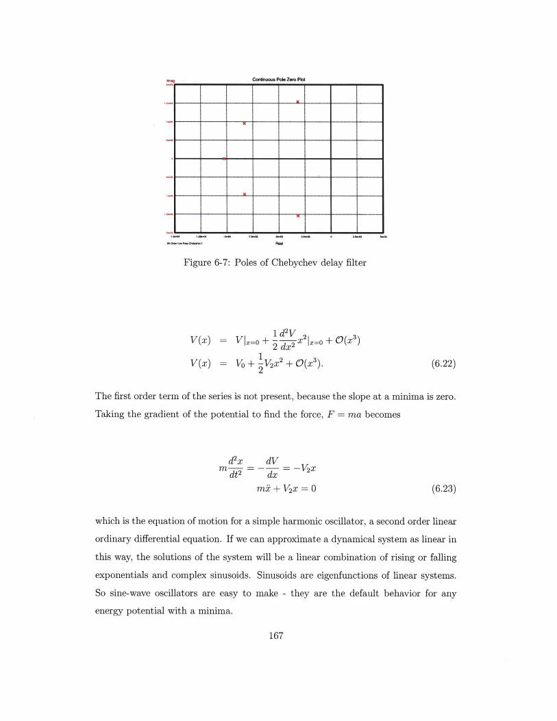
COriWuo Poe ZerO Plot
Figure 6-7: Poles of Chebychev delay filter
V(x)
V(x)
VIX=0 + X 2|X=0+0(x3 )2 dx 2
1= Vo+ -V 2 x 2 + O(X3 ).
2(6.22)
The first order term of the series is not present, because the slope at a minima is zero.
Taking the gradient of the potential to find the force, F = ma becomes
d2x dVm-- - - -V 2 x
dt2 dx V
mz- +V 2x = 0 (6.23)
which is the equation of motion for a simple harmonic oscillator, a second order linear
ordinary differential equation. If we can approximate a dynamical system as linear in
this way, the solutions of the system will be a linear combination of rising or falling
exponentials and complex sinusoids. Sinusoids are eigenfunctions of linear systems.
So sine-wave oscillators are easy to make - they are the default behavior for any
energy potential with a minima.
167
I
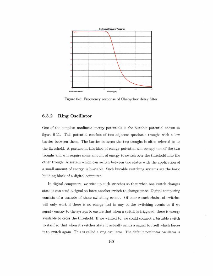
Continuous Frequency Response
MtOrdriPmae bw FM (")
Figure 6-8: Frequency response of Chebychev delay filter
6.3.2 Ring Oscillator
One of the simplest nonlinear energy potentials is the bistable potential shown in
figure 6-11. This potential consists of two adjacent quadratic troughs with a low
barrier between them. The barrier between the two troughs is often referred to as
the threshold. A particle in this kind of energy potential will occupy one of the two
troughs and will require some amount of energy to switch over the threshold into the
other trough. A system which can switch between two states with the application of
a small amount of energy, is bi-stable. Such bistable switching systems are the basic
building block of a digital computer.
In digital computers, we wire up such switches so that when one switch changes
state it can send a signal to force another switch to change state. Digital computing
consists of a cascade of these switching events. Of course such chains of switches
will only work if there is no energy lost in any of the switching events or if we
supply energy to the system to ensure that when a switch is triggered, there is energy
available to cross the threshold. If we wanted to, we could connect a bistable switch
to itself so that when it switches state it actually sends a signal to itself which forces
it to switch again. This is called a ring oscillator. The default nonlinear oscillator is
168
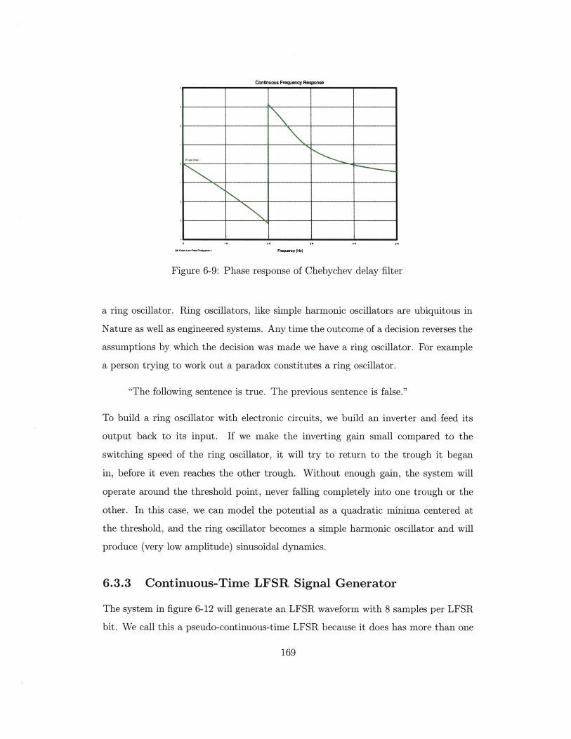
Connuous Frequency Aetponse
Figure 6-9: Phase response of Chebychev delay filter
a ring oscillator. Ring oscillators, like simple harmonic oscillators are ubiquitous in
Nature as well as engineered systems. Any time the outcome of a decision reverses the
assumptions by which the decision was made we have a ring oscillator. For example
a person trying to work out a paradox constitutes a ring oscillator.
"The following sentence is true. The previous sentence is false."
To build a ring oscillator with electronic circuits, we build an inverter and feed its
output back to its input. If we make the inverting gain small compared to the
switching speed of the ring oscillator, it will try to return to the trough it began
in, before it even reaches the other trough. Without enough gain, the system will
operate around the threshold point, never falling completely into one trough or the
other. In this case, we can model the potential as a quadratic minima centered at
the threshold, and the ring oscillator becomes a simple harmonic oscillator and will
produce (very low amplitude) sinusoidal dynamics.
6.3.3 Continuous-Time LFSR Signal Generator
The system in figure 6-12 will generate an LFSR waveform with 8 samples per LFSR
bit. We call this a pseudo-continuous-time LFSR because it does has more than one
169
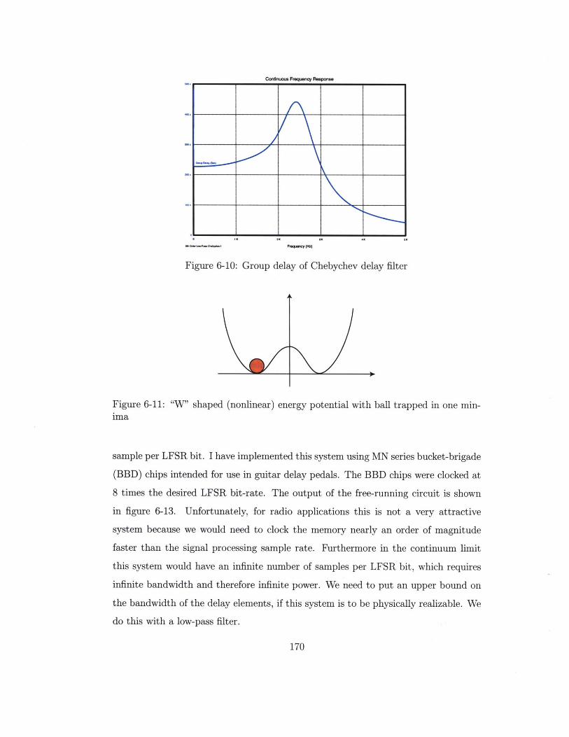
Continuous Frequency Retponse
Figure 6-10: Group del ay of Chebychev delay filter
Figure 6-11: "W" shapedima
(nonlinear) energy potential with ball trapped in one min-
sample per LFSR bit. I have implemented this system using MN series bucket-brigade
(BBD) chips intended for use in guitar delay pedals. The BBD chips were clocked at
8 times the desired LFSR bit-rate. The output of the free-running circuit is shown
in figure 6-13. Unfortunately, for radio applications this is not a very attractive
system because we would need to clock the memory nearly an order of magnitude
faster than the signal processing sample rate. Furthermore in the continuum limit
this system would have an infinite number of samples per LFSR bit, which requires
infinite bandwidth and therefore infinite power. We need to put an upper bound on
the bandwidth of the delay elements, if this system is to be physically realizable. We
do this with a low-pass filter.
170
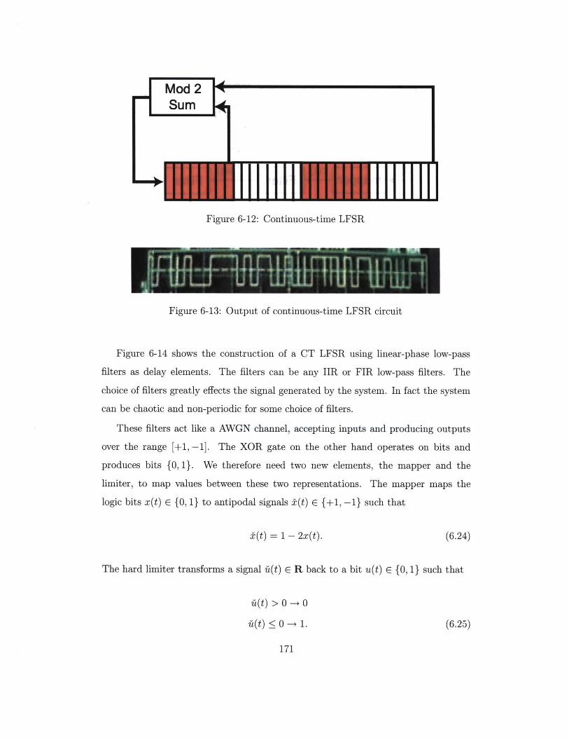
Figure 6-12: Continuous-time LFSR
Figure 6-13: Output of continuous-time LFSR circuit
Figure 6-14 shows the construction of a CT LFSR using linear-phase low-pass
filters as delay elements. The filters can be any IIR or FIR low-pass filters. The
choice of filters greatly effects the signal generated by the system. In fact the system
can be chaotic and non-periodic for some choice of filters.
These filters act like a AWGN channel, accepting inputs and producing outputs
over the range [+1, -1]. The XOR gate on the other hand operates on bits and
produces bits {0, 1}. We therefore need two new elements, the mapper and the
limiter, to map values between these two representations. The mapper maps the
logic bits x(t) E {0, 1} to antipodal signals t(t) E {+1, -1} such that
±(t) = 1 - 2x(t). (6.24)
The hard limiter transforms a signal ft(t) E R back to a bit u(t) E {, 1} such that
ft(t) > 0 -+ 0
fi(t) < 0 -+ 1. (6.25)
171
I
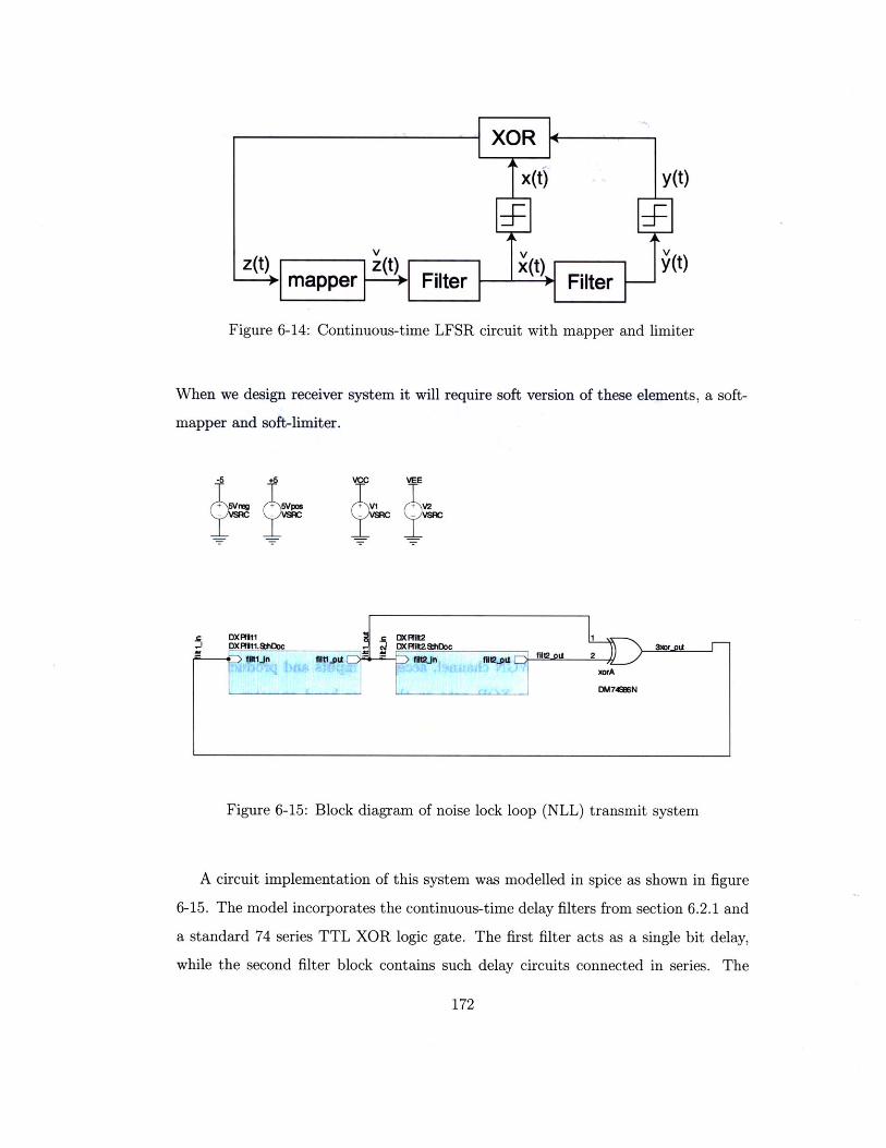
x(t) yz
V y-+t J_mapper Filter F~) ilter
Figure 6-14: Continuous-time LFSR circuit with mapper and limiter
When we design receiver system it will require soft version of these elements, a soft-
mapper and soft-limiter.
-5 +5V V+C VEE
Figure 6-15: Block diagram of noise lock loop (NLL) transmit system
A circuit implementation of this system was modelled in spice as shown in figure
6-15. The model incorporates the continuous-time delay filters from section 6.2.1 and
a standard 74 series TTL XOR logic gate. The first filter acts as a single bit delay,
while the second filter block contains such delay circuits connected in series. The
172
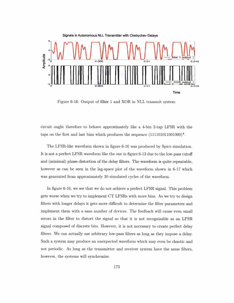
Signals in Autonomous NLL Transmitter with Chebychev Delays
I L/V VV U VV U VViU. VUV' fr
0 0.005 0.01 0.015
Time
Figure 6-16: Output of filter 1 and XOR in NLL transmit system
circuit ought therefore to behave approximately like a 4-bin 2-tap LFSR with the
taps on the first and last bins which produces the sequence (111101011001000)*.
The LFSR-like waveform shown in figure 6-16 was produced by Spice simulation.
It is not a perfect LFSR waveform like the one in figure 6-13 due to the low-pass cutoff
and (minimal) phase distortion of the delay filters. The waveform is quite repeatable,
however as can be seen in the lag-space plot of the waveform shown in 6-17 which
was generated from approximately 30 simulated cycles of the waveform.
In figure 6-16, we see that we do not achieve a perfect LFSR signal. This problem
gets worse when we try to implement CT LFSRs with more bins. As we try to design
filters with longer delays it gets more difficult to determine the filter parameters and
implement them with a sane number of devices. The feedback will cause even small
errors in the filter to distort the signal so that it is not recognizable as an LFSR
signal composed of discrete bits. However, it is not necessary to create perfect delay
filters. We can actually use arbitrary low-pass filters as long as they impose a delay.
Such a system may produce an unexpected waveform which may even be chaotic and
not periodic. As long as the transmitter and receiver system have the same filters,
however, the systems will synchronize.
173
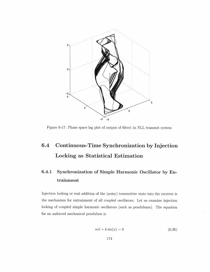
5
-55
5
00
-5 -5
Figure 6-17: Phase space lag plot of output of filter1 in NLL transmit system
6.4 Continuous-Time Synchronization by Injection
Locking as Statistical Estimation
6.4.1 Synchronization of Simple Harmonic Oscillator by En-
trainment
Injection locking or real addition of the (noisy) transmitter state into the receiver is
the mechanism for entrainment of all coupled oscillators. Let us examine injection
locking of coupled simple harmonic oscillators (such as pendulums). The equation
for an unforced mechanical pendulum is
mz + k sin(x) = 0 (6.26)
174
For small angles of deflection, we can approximate sin(x) by x leaving he equation
for a simple harmonic oscillator (SHO)
mz + kx = 0. (6.27)
Setting m = k =1
x + X = 0 (6.28)
We will parameterize this second order differential equation as two first order differ-
ential equations by defining
zo X 'k
x1 _ 'O.
(6.29)
(6.30)
(6.31)
Equation (6.28) then becomes
i1 + x0 = 0
zo = -Y1 (6.32)
(6.33)
It can now be written as a system of first order ordinary differential equations (ODE).
X1 = 'e0
zo = -x1. (6.34)
(6.35)
The factor graph for two coupled SHO is therefore given by figure 6-18. Drawing the
factor graph for a SHO required a rather strange function node, the time derivative.
But what does it mean to take the derivative of a probability? The definition of the
175
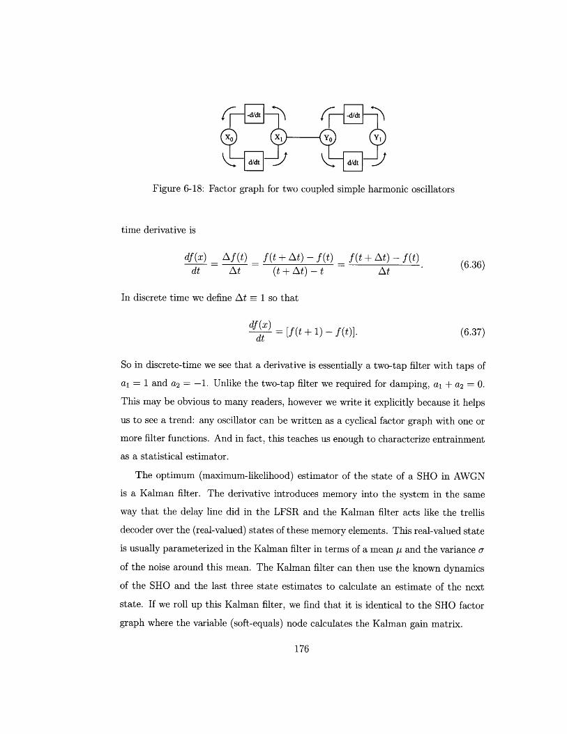
-d/dt] -d/dt
d/dt] d/dt
Figure 6-18: Factor graph for two coupled simple harmonic oscillators
time derivative is
df(x) _ Af(t) f(t + At) - f(t) _ f(t + At) - f(t)dt At (t + At) - t At(
In discrete time we define At 1 so that
df(x)dt [f(t + 1) - f(t)]. (6.37)
So in discrete-time we see that a derivative is essentially a two-tap filter with taps of
ai = 1 and a2 = -1. Unlike the two-tap filter we required for damping, ai + a2 = 0.
This may be obvious to many readers, however we write it explicitly because it helps
us to see a trend: any oscillator can be written as a cyclical factor graph with one or
more filter functions. And in fact, this teaches us enough to characterize entrainment
as a statistical estimator.
The optimum (maximum-likelihood) estimator of the state of a SHO in AWGN
is a Kalman filter. The derivative introduces memory into the system in the same
way that the delay line did in the LFSR and the Kalman filter acts like the trellis
decoder over the (real-valued) states of these memory elements. This real-valued state
is usually parameterized in the Kalman filter in terms of a mean y and the variance -
of the noise around this mean. The Kalman filter can then use the known dynamics
of the SHO and the last three state estimates to calculate an estimate of the next
state. If we roll up this Kalman filter, we find that it is identical to the SHO factor
graph where the variable (soft-equals) node calculates the Kalman gain matrix.
176
6.4.2 Noise Lock Loop Tracking by Injection Locking
A digital software radio must estimate the phase of the transmitter's bit clock in order
to properly sample the code bits. This synchronization function is known as tracking.
In a software radio tracking is a separate function performed by a system such as a
PLL, DLL or Tau-Dither Loop. The DT NLL performs acquisition, but it needs to
be clocked synchronously with the transmitter's LFSR in order to do this. We might
hope that if implemented with CT circuits, it might also be able to perform tracking
without an external tracking loop. The NLL would then not only estimate the state
of the transmit LFSR, but also entrain to its bit clock. This would be useful, because
then we would get tracking essentially for free by implementing the DT algorithm
with CT circuits. It might also lead to more robust hand-off between acquisition and
tracking which are separate functions in digital software radios.
Synchronization of coupled continuous-time oscillators occurs by entrainment. En-
trainment requires that the coupled oscillators (or at least the "receive" oscillator)
be dissipative. Dissipation means that the volume of the phase space of the entire
coupled system must shrink over time. With coupled linear oscillators, the dissipation
could be friction - energy lost to heat. With coupled nonlinear oscillators, the dissipa-
tion can be provided by the nonlinearity itself. In either case, coupling the oscillators
involves summing a small amount of the state of one of the independent variables
from the "transmit" oscillator into the equivalent state in the receive oscillator.
In electronic systems, coupling two oscillators by adding some of the output of
one oscillator to the input of another oscillator is called injection locking. This is just
real addition of the (attenuated) transmitter's signal to the receiver's signal. Injec-
tion locking has been used in electronics to produce extremely stable high-frequency
sinusoidal oscillators by injecting the output of a digital clock into a sinusoidal ring
oscillator. When driven by a square wave, the ring oscillator still produces a sinusoid,
but with decreased phase jitter [4].
The CT NLL receiver system is shown in figure 6-19. The soft-xor and channel
model p(ylx) have been explained previously. The soft-mapper is a probabilistic
177
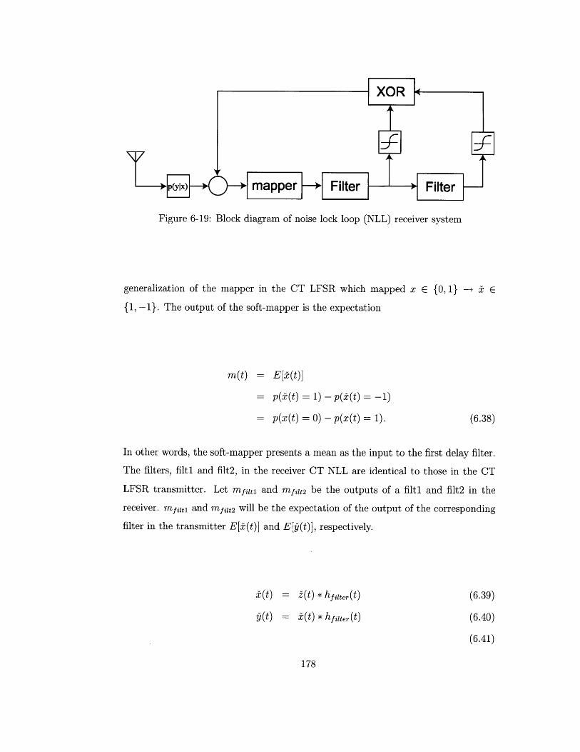
Figure 6-19: Block diagram of noise lock loop (NLL) receiver system
generalization of the mapper in the CT LFSR which mapped x E {o, 1} -+
{1, -1}. The output of the soft-mapper is the expectation
m (t) = E[it(t)]
= p(f (t) = 1) - p(f(t) = -1)
= p((t) = 0) - p((t) = 1). (6.38)
In other words, the soft-mapper presents a mean as the input to the first delay filter.
The filters, filt1 and filt2, in the receiver CT NLL are identical to those in the CT
LFSR transmitter. Let mfiltl and mfilt2 be the outputs of a filt1 and filt2 in the
receiver. mfilt and mfiu2 will be the expectation of the output of the corresponding
filter in the transmitter E[i(t)] and E[y(t)], respectively.
(t) = (t) * hfilter(t) (6.39)
(t) =i(t) * hfilter(t) (6.40)
(6.41)
178
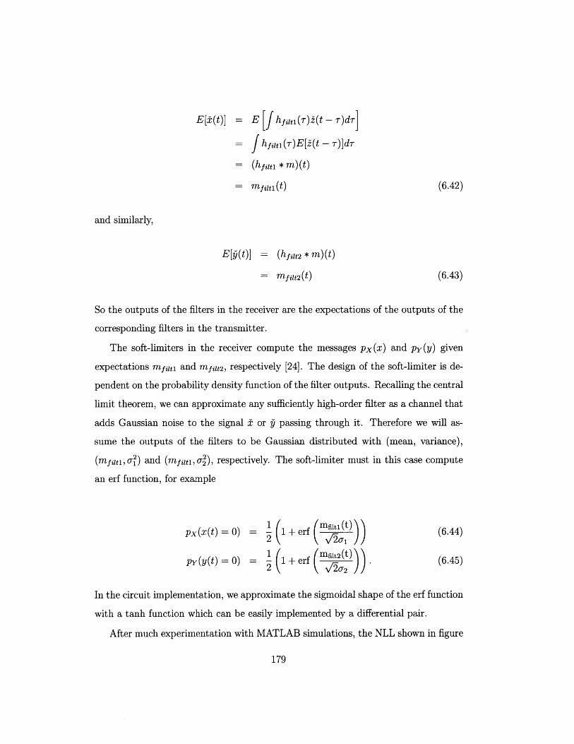
E[t(t)] = E J hfjti(T)2(t - T)d-r
J hf 1,nQ)E[z(t - 7)]dT
= (hfint, * m)(t)
mpiti(t) (6.42)
and similarly,
E[Q(t)] = (hfilt2 * m)(t)
= mffil2(t) (6.43)
So the outputs of the filters in the receiver are the expectations of the outputs of the
corresponding filters in the transmitter.
The soft-limiters in the receiver compute the messages px(x) and py(y) given
expectations mfilti and mfilu2, respectively [24]. The design of the soft-limiter is de-
pendent on the probability density function of the filter outputs. Recalling the central
limit theorem, we can approximate any sufficiently high-order filter as a channel that
adds Gaussian noise to the signal t or p passing through it. Therefore we will as-
sume the outputs of the filters to be Gaussian distributed with (mean, variance),
(mfiti, o ) and (mfiltl, U2), respectively. The soft-limiter must in this case compute
an erf function, for example
px(x(t) = 0) 1 + erf (6.44)
py(y(t) = 0) = 1 + erf (6.45)
In the circuit implementation, we approximate the sigmoidal shape of the erf function
with a tanh function which can be easily implemented by a differential pair.
After much experimentation with MATLAB simulations, the NLL shown in figure
179
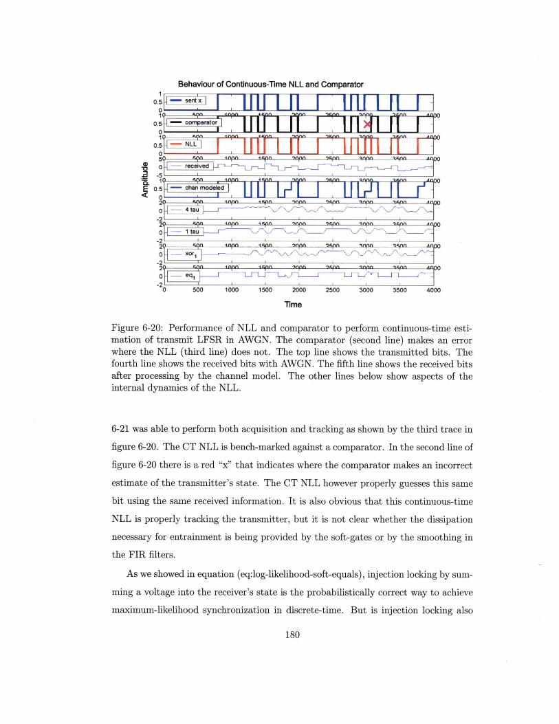
Behaviour of Continuous-Time NLL and Comparator
0.5 0 - LJ0.5 922 SOWT$JAT00r 2 1'1H 0 fF&A VTAn0
o , E E E . u H I_ -1u 1 I1E0.
. 5E 0. ;iZ ;ik-'d II .JI11
<I 0 LJ. L YU LLI'T0 4a
2 * 4AftA 4 iseo WPO~ mkfpoI 'A"lf taplj
0 1 tau
-2- L
o -eq LA L2 } L JL L-i I
-20 500 1000 1500 2000 2500 3000 3500 4000
Time
Figure 6-20: Performance of NLL and comparator to perform continuous-time esti-mation of transmit LFSR in AWGN. The comparator (second line) makes an errorwhere the NLL (third line) does not. The top line shows the transmitted bits. Thefourth line shows the received bits with AWGN. The fifth line shows the received bitsafter processing by the channel model. The other lines below show aspects of theinternal dynamics of the NLL.
6-21 was able to perform both acquisition and tracking as shown by the third trace in
figure 6-20. The CT NLL is bench-marked against a comparator. In the second line of
figure 6-20 there is a red "x" that indicates where the comparator makes an incorrect
estimate of the transmitter's state. The CT NLL however properly guesses this same
bit using the same received information. It is also obvious that this continuous-time
NLL is properly tracking the transmitter, but it is not clear whether the dissipation
necessary for entrainment is being provided by the soft-gates or by the smoothing in
the FIR filters.
As we showed in equation (eq:log-likelihood-soft-equals), injection locking by sum-
ming a voltage into the receiver's state is the probabilistically correct way to achieve
maximum-likelihood synchronization in discrete-time. But is injection locking also
180
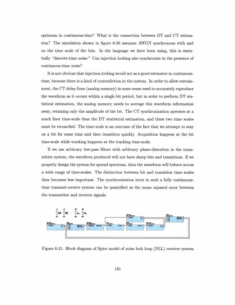
optimum in continuous-time? What is the connection between DT and CT estima-
tion? The simulation shown in figure 6-20 assumes AWGN synchronous with and
on the time scale of the bits. In the language we have been using, this is essen-
tially "discrete-time noise." Can injection locking also synchronize in the presence of
continuous-time noise?
It is not obvious that injection locking would act as a good estimator in continuous-
time, because there is a kind of contradiction in the system. In order to allow entrain-
ment, the CT delay-lines (analog memory) in some sense need to accurately reproduce
the waveform as it occurs within a single bit period, but in order to perform DT sta-
tistical estimation, the analog memory needs to average this waveform information
away, retaining only the amplitude of the bit. The CT synchronization operates at a
much finer time-scale than the DT statistical estimation, and these two time scales
must be reconciled. The time scale is an outcome of the fact that we attempt to stay
on a bit for some time and then transition quickly. Acquisition happens at the bit
time-scale while tracking happens at the tracking time-scale.
If we use arbitrary low-pass filters with arbitrary phase-distortion in the trans-
mitter system, the waveform produced will not have sharp bits and transitions. If we
properly design the system for spread spectrum, then the waveform will behave across
a wide range of time-scales. The distinction between bit and transition time scales
then becomes less important. The synchronization error in such a fully continuous-
time transmit-receive system can be quantified as the mean squared error between
the transmitter and receiver signals.
~.c~mc
Figure 6-21: Block diagram of Spice model of noise lock loop (NLL) receiver system
181

182
Chapter 7
Systems
"Most verification of VLSI designs, synchronous and asynchronous, as-
sumes discrete models discrete models for signal values and transition
times. These discrete models lend themselves well to event-driven simu-
lation, model checking, and theorem proving. However, many important
circuit phenomenon cannot be modelled with discrete time and values,
and failure to account for these phenomena can lead to faulty designs.
These problems are especially apparent in the design of asynchronous cir-
cuits where computation is driven by internal events and not regulated
by an external clock. This has led to many heuristic guidelines for de-
signing such circuits referring to such things as "monotonic transitions,"
"isochronic forks," and debates of "interleaving semantics" versus "true
concurrency." Underlying these issues is a more basic question, "can dis-
crete models of circuit behavior be based on a physically sound model of
circuit behavior?" [17]
7.1 Extending Digital Primitives with Soft-Gates
We have seen that we can abstract the truth table of any digital logic gate into
a probabilistic soft-gate. We might therefore be curious what would happen if we
attempt to combine these probabilistic logic primitives to create probabilistic versions
183
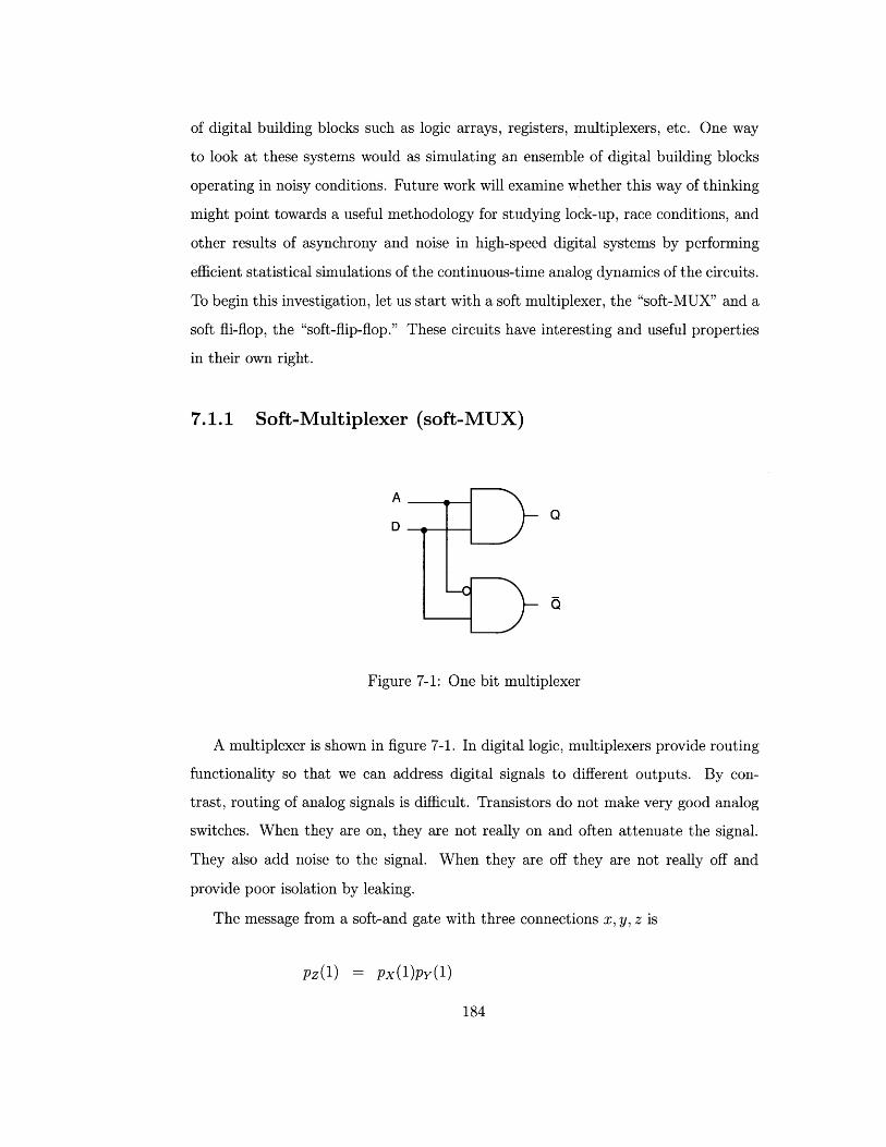
of digital building blocks such as logic arrays, registers, multiplexers, etc. One way
to look at these systems would as simulating an ensemble of digital building blocks
operating in noisy conditions. Future work will examine whether this way of thinking
might point towards a useful methodology for studying lock-up, race conditions, and
other results of asynchrony and noise in high-speed digital systems by performing
efficient statistical simulations of the continuous-time analog dynamics of the circuits.
To begin this investigation, let us start with a soft multiplexer, the "soft-MUX" and a
soft fli-flop, the "soft-flip-flop." These circuits have interesting and useful properties
in their own right.
7.1.1 Soft-Multiplexer (soft-MUX)
AQ
D .-
Figure 7-1: One bit multiplexer
A multiplexer is shown in figure 7-1. In digital logic, multiplexers provide routing
functionality so that we can address digital signals to different outputs. By con-
trast, routing of analog signals is difficult. Transistors do not make very good analog
switches. When they are on, they are not really on and often attenuate the signal.
They also add noise to the signal. When they are off they are not really off and
provide poor isolation by leaking.
The message from a soft-and gate with three connections x, y, z is
Pz(1) = Px(1)Py(l)
184
Pz(O) = px(O)py(O) +px(O)py(1) +px(1)py(O). (7.1)
We might wonder what would happen if we build a multiplexer with soft-and gates
instead of digital and gates. Could such a circuit be useful for routing analog signals?
If we naively pursue such a circuit, we do get a circuit which passes the analog currents
in an addressable manner. The addressed output produces a (normalized) copy of
the input signal.
We find that the output from the other soft-and gate, however, has an output of
(pz(O) = I, pz(1) = 0). This is not precisely what we want. We would like the gate
that is off to output nothing, i.e. (px(O) = .5,px(l) = .5). We can accomplish this
with a modified soft-and gate that obeys the equation,
pz(1) = px()py( 1)+ px(O)py(0) +px(O)py(1)
pz(O) = px(O)py(O)+px(0)py(1)+px(1)py(O), (7.2)
Let x be the address signal and y be the data signal. Let us examine only one modified
soft-and in the soft-multiplexer - say the one with the Q output in figure 7-1. If x = 1,
then px(0) = 0, px(1) = 1 which means that the output of the soft-and gate mirrors
the y input,
Pz(1) = py(1)
Pz(0) = py(0). (7.3)
But if x = 0, then px(0) = 1, px(1) = 0. This means that the other modified soft-and
should be mirroring the data signal. The Q modified soft-and does the right thing.
pz(1) = py (0) + py (1) = 1
pz(0) = pY(0)+ p(1)= 1. (7.4)
185
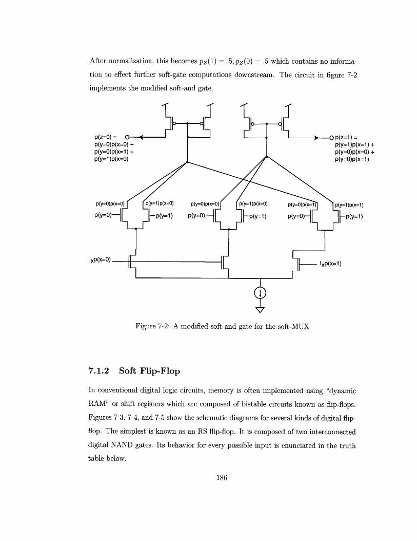
After normalization, this becomes pz(1) = .5, pz(0) = .5 which contains no informa-
tion to effect further soft-gate computations downstream. The circuit in figure 7-2
implements the modified soft-and gate.
p(z=O) = C O p(z=1) =
p(y=O)p(x=O) + p(y=1)p(x=1) +p(y=O)p(x=1) + p(y=O)p(x=O) +p(y=1)p(x=O) p(y=O)p(x=1)
p(y=O)p(x=O) p(y=1)p(x=O) p(y=O)p(x=O) p(y=1)p(x=O) p(y=O)p(x=1) p(y=1)p(x=1)
p(y=0) p(y=1) p(y=0) - p(y=1) p(y=0) kp(y=1)
Figure 7-2: A modified soft-and gate for the soft-MUX
7.1.2 Soft Flip-Flop
In conventional digital logic circuits, memory is often implemented using "dynamic
RAM" or shift registers which are composed of bistable circuits known as flip-flops.
Figures 7-3, 7-4, and 7-5 show the schematic diagrams for several kinds of digital flip-
flop. The simplest is known as an RS flip-flop. It is composed of two interconnected
digital NAND gates. Its behavior for every possible input is enunciated in the truth
table below.
186
. I~ -_ - 1V.NjV*j1* - .- - - . .1 1 1 -
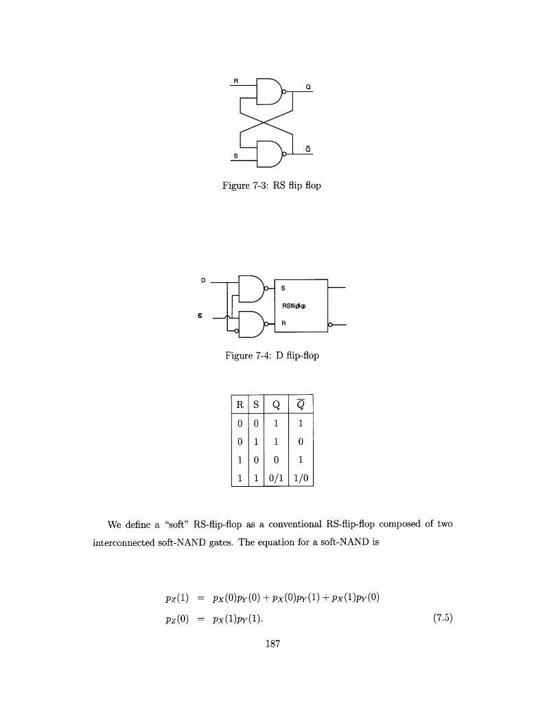
Figure 7-3: RS flip flop
Figure 7-4: D flip-flop
0 0 1 1
1 1 0/1
0
1
1/0
We define a "soft" RS-flip-flop as a conventional RS-flip-flop composed of two
interconnected soft-NAND gates. The equation for a soft-NAND is
Pz(1) = Px (O)PY (0) + px(O)py(1) + px (1)py(0)
pz(0) = px(1)pY (1).
187
(7.5)
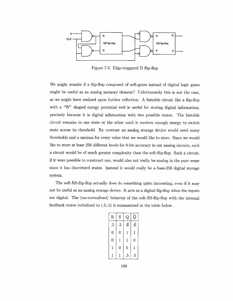
D
CLK
Figure 7-5: Edge-triggered D flip-flop
We might wonder if a flip-flop composed of soft-gates instead of digital logic gates
might be useful as an analog memory element? Unfortunately this is not the case,
as we might have realized upon further reflection. A bistable circuit like a flip-flop
with a "W" shaped energy potential well is useful for storing digital information,
precisely because it is digital information with two possible states. The bistable
circuit remains in one state or the other until it receives enough energy to switch
state across its threshold. By contrast an analog storage device would need many
thresholds and a minima for every value that we would like to store. Since we would
like to store at least 256 different levels for 8-bit accuracy in our analog circuits, such
a circuit would be of much greater complexity than the soft-flip-flop. Such a circuit,
if it were possible to construct one, would also not really be analog in the pure sense
since it has discretized states. Instead it would really be a base-256 digital storage
system.
The soft-RS-flip-flop actually does do something quite interesting, even if it may
not be useful as an analog storage device. It acts as a digital flip-flop when the inputs
are digital. The (un-normalized) behavior of the soft-RS-flip-flop with the internal
feedback states initialized to (.5,.5) is summarized in the table below.
R S Q Q
.5 .5 .6 .6
0 0 1 1
0 1 1 0
1 0 0 1
1 1 .5 .5
188
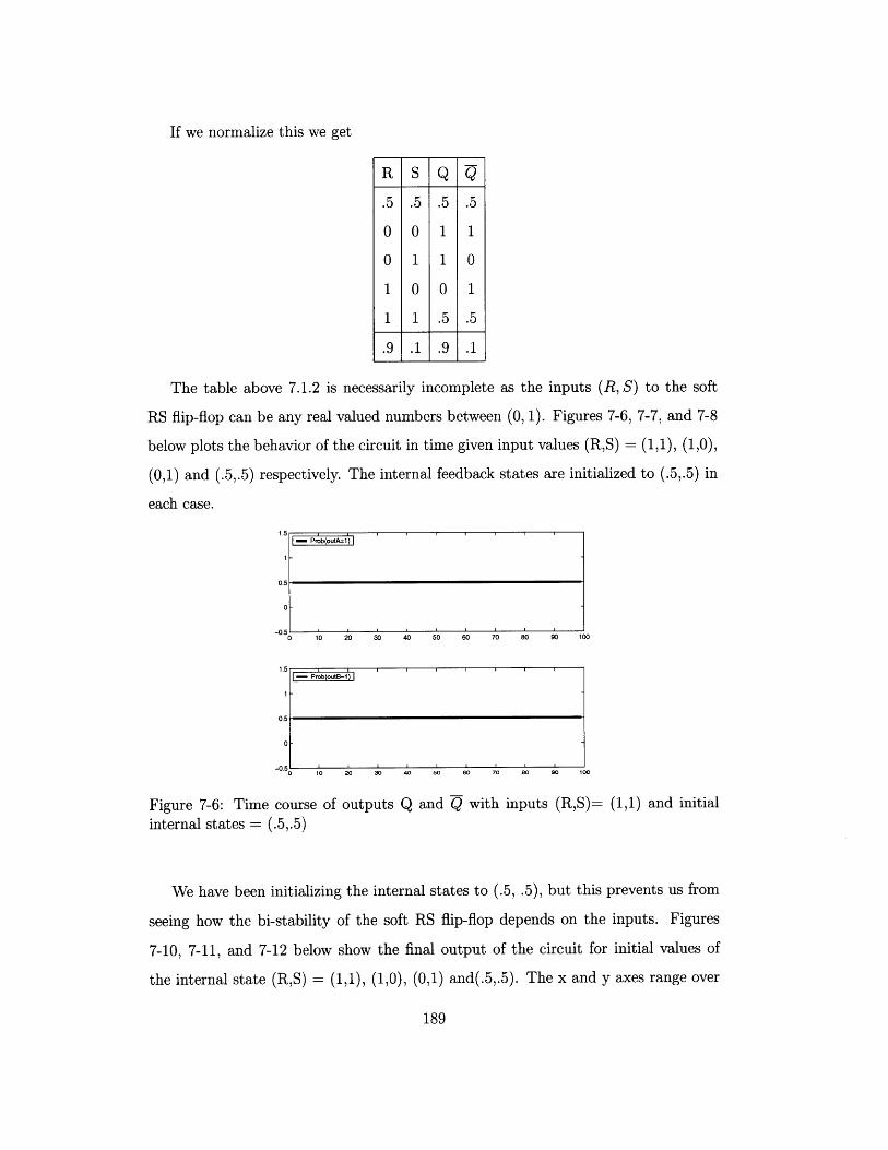
If we normalize this we get
R S Q Q
.5 .5 .5 .5
0 0 1 1
0 1 1 0
1 0 0 1
1 1 .5 .5
.9 .1 .9 .1
The table above 7.1.2 is necessarily incomplete as the inputs (R, S) to the soft
RS flip-flop can be any real valued numbers between (0, 1). Figures 7-6, 7-7, and 7-8
below plots the behavior of the circuit in time given input values (R,S) = (1,1), (1,0),
(0,1) and (.5,.5) respectively. The internal feedback states are initialized to (.5,.5) in
each case.
1.5Prob(outA=1)
0.5
0-
0 io 40 50 70 90 100
Prob(otB=-1)
1 -
0.5-
0-
-0. -I
o05 io 20 50 60 70 80 90 100
Figure 7-6: Time course of outputs Q and Q with inputs (R,S)= (1,1) and initialinternal states = (.5,.5)
We have been initializing the internal states to (.5, .5), but this prevents us from
seeing how the bi-stability of the soft RS flip-flop depends on the inputs. Figures
7-10, 7-11, and 7-12 below show the final output of the circuit for initial values of
the internal state (R,S) = (1,1), (1,0), (0,1) and(.5,.5). The x and y axes range over
189
I 11---__- -- _ - ,- - 4 - - I - 1 -1- - _-1-1-- . -__ -, - .1---l- -. , , , .1 1 1 -_ _ I
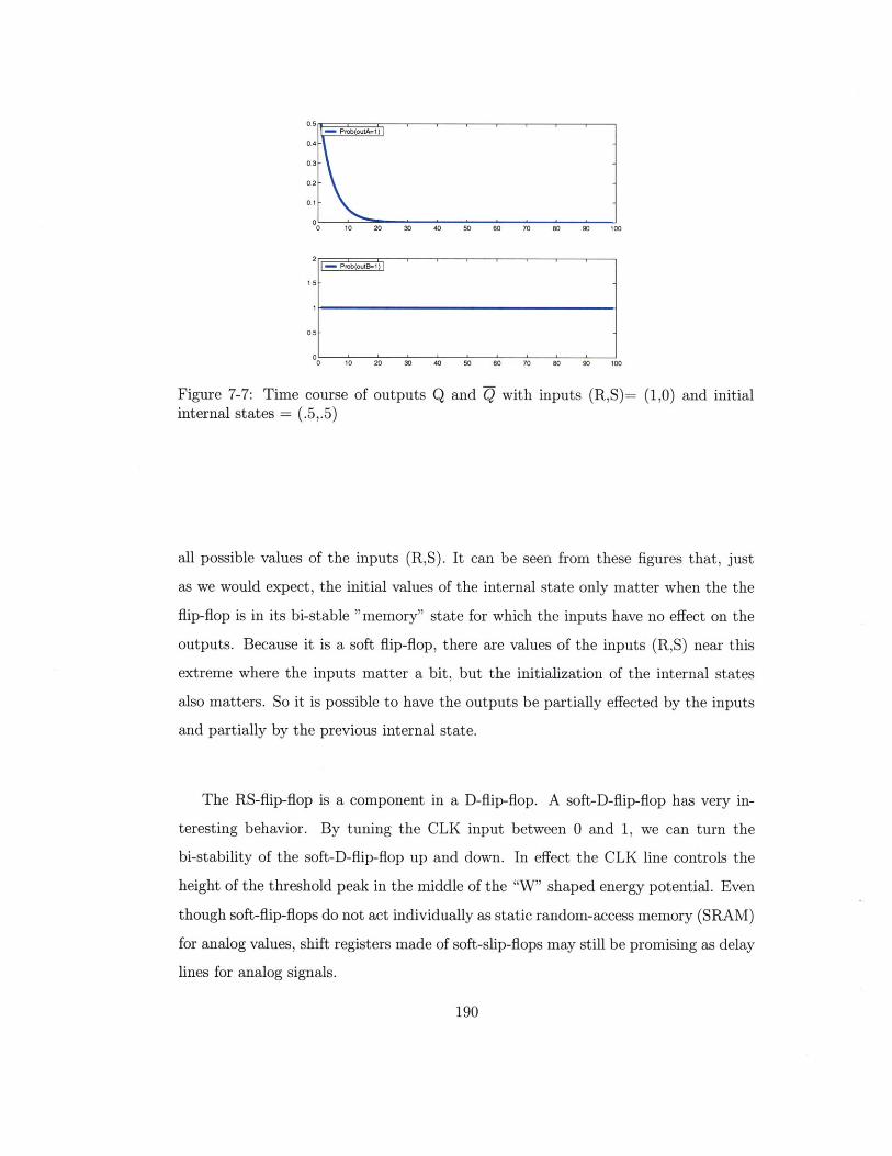
- Prg(outA=1)
0.4-
0.3-
0.2-
0 1-
0 10 20 30 40 50 60 70 80 90 100
2-== Pro(outB=1)
1.5-
0.5-
0 10 20 30 40 50 60 70 80 90 100
Figure 7-7: Time course of outputs Q and Q with inputs (R,S)= (1,0) and initialinternal states = (.5,.5)
all possible values of the inputs (R,S). It can be seen from these figures that, just
as we would expect, the initial values of the internal state only matter when the the
flip-flop is in its bi-stable "memory" state for which the inputs have no effect on the
outputs. Because it is a soft flip-flop, there are values of the inputs (R,S) near this
extreme where the inputs matter a bit, but the initialization of the internal states
also matters. So it is possible to have the outputs be partially effected by the inputs
and partially by the previous internal state.
The RS-flip-flop is a component in a D-flip-flop. A soft-D-flip-flop has very in-
teresting behavior. By tuning the CLK input between 0 and 1, we can turn the
bi-stability of the soft-D-flip-flop up and down. In effect the CLK line controls the
height of the threshold peak in the middle of the "W" shaped energy potential. Even
though soft-flip-flops do not act individually as static random-access memory (SRAM)
for analog values, shift registers made of soft-slip-flops may still be promising as delay
lines for analog signals.
190
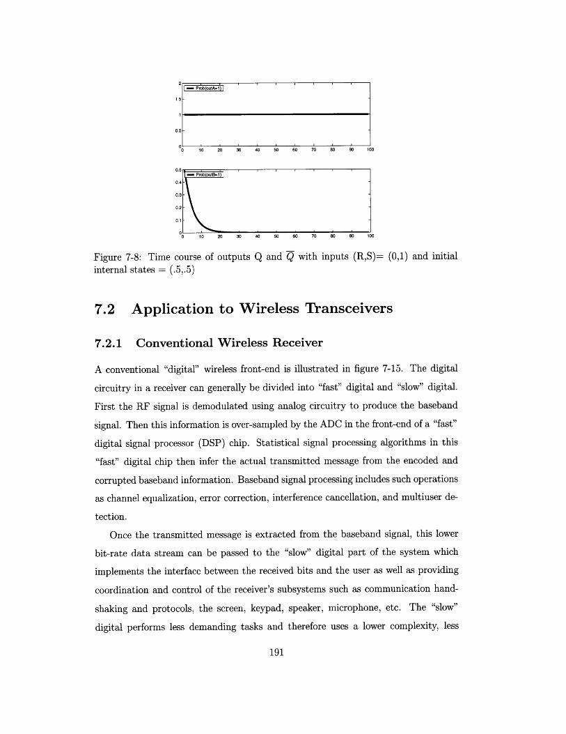
2-
1.5-
1*
0.5-
0 10 20 30 40 50 60 70 90 100
0.-= - Prob(outB=1)
04-
0.3-
0.2-
0.1-
0 10 20 30 40 50 60 70 80 90 100
Figure 7-8: Time course of outputs Q and Q with inputs (R,S)= (0,1) and initialinternal states = (.5,.5)
7.2 Application to Wireless Transceivers
7.2.1 Conventional Wireless Receiver
A conventional "digital" wireless front-end is illustrated in figure 7-15. The digital
circuitry in a receiver can generally be divided into "fast" digital and "slow" digital.
First the RF signal is demodulated using analog circuitry to produce the baseband
signal. Then this information is over-sampled by the ADC in the front-end of a "fast"
digital signal processor (DSP) chip. Statistical signal processing algorithms in this
"fast" digital chip then infer the actual transmitted message from the encoded and
corrupted baseband information. Baseband signal processing includes such operations
as channel equalization, error correction, interference cancellation, and multiuser de-
tection.
Once the transmitted message is extracted from the baseband signal, this lower
bit-rate data stream can be passed to the "slow" digital part of the system which
implements the interface between the received bits and the user as well as providing
coordination and control of the receiver's subsystems such as communication hand-
shaking and protocols, the screen, keypad, speaker, microphone, etc. The "slow"
digital performs less demanding tasks and therefore uses a lower complexity, less
191
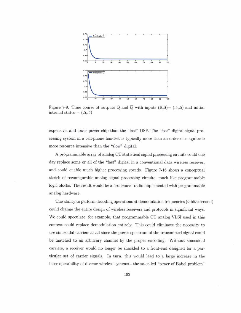
1- Prob(outA-1)
0,74
0.72-
0.7-
0.68 -
0.66 1 10 10 20 30 40 50 60 70 80 90 100
0.76j- Prob out8=1l
0.74
0.72-
0.7-
0.68-
0 >0 20 30 40 50 0 70 80 90 100
Figure 7-9: Time course of outputs Q and Q with inputs (R,S)= (.5,.5) and initialinternal states = (.5,.5)
expensive, and lower power chip than the "fast" DSP. The "fast" digital signal pro-
cessing system in a cell-phone handset is typically more than an order of magnitude
more resource intensive than the "slow" digital.
A programmable array of analog CT statistical signal processing circuits could one
day replace some or all of the "fast" digital in a conventional data wireless receiver,
and could enable much higher processing speeds. Figure 7-16 shows a conceptual
sketch of reconfigurable analog signal processing circuits, much like programmable
logic blocks. The result would be a "software" radio implemented with programmable
analog hardware.
The ability to perform decoding operations at demodulation frequencies (Gbits/second)
could change the entire design of wireless receivers and protocols in significant ways.
We could speculate, for example, that programmable CT analog VLSI used in this
context could replace demodulation entirely. This could eliminate the necessity to
use sinusoidal carriers at all since the power spectrum of the transmitted signal could
be matched to an arbitrary channel by the proper encoding. Without sinusoidal
carriers, a receiver would no longer be shackled to a front-end designed for a par-
ticular set of carrier signals. In turn, this would lead to a large increase in the
inter-operability of diverse wireless systems - the so-called "tower of Babel problem"
192
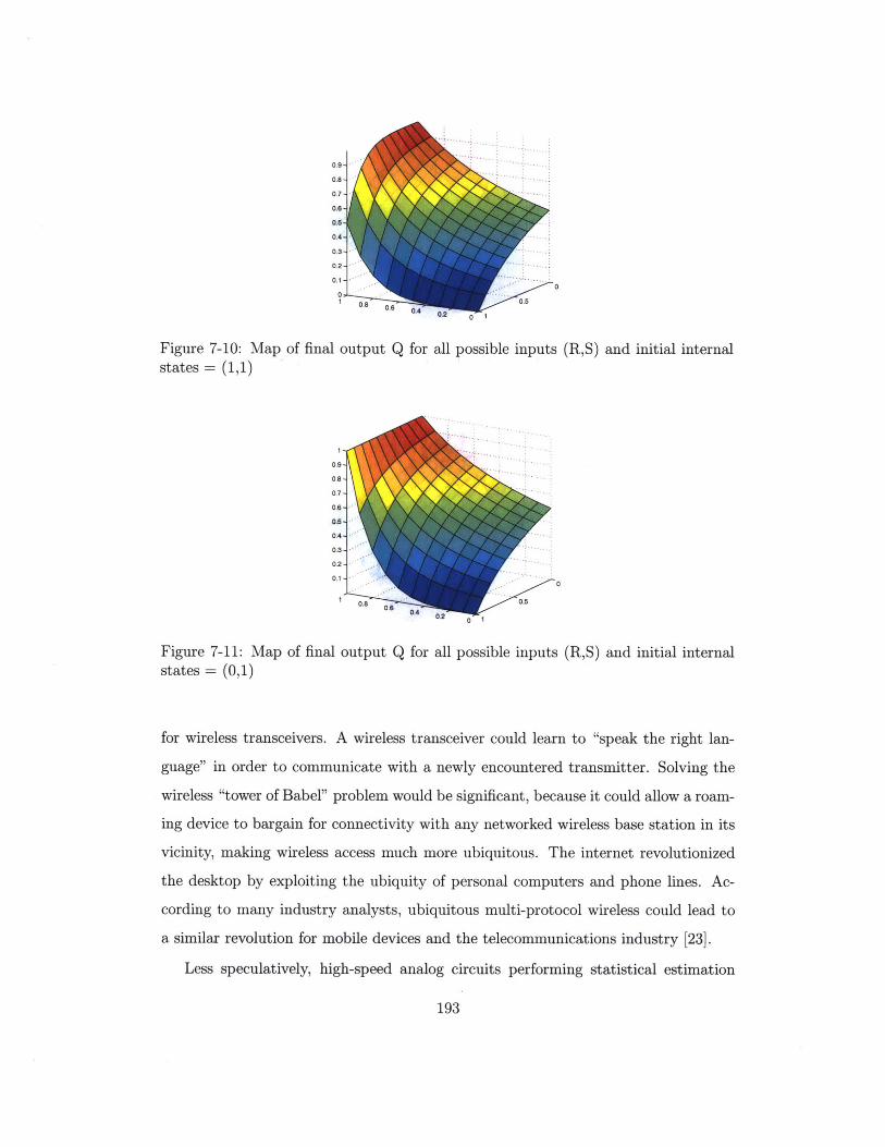
Figure 7-10: Map of final output Q for all possible inputs (R,S) and initial internalstates = (1,1)
Figure 7-11: Map of final output Qstates = (0,1)
for all possible inputs (R,S) and initial internal
for wireless transceivers. A wireless transceiver could learn to "speak the right lan-
guage" in order to communicate with a newly encountered transmitter. Solving the
wireless "tower of Babel" problem would be significant, because it could allow a roam-
ing device to bargain for connectivity with any networked wireless base station in its
vicinity, making wireless access much more ubiquitous. The internet revolutionized
the desktop by exploiting the ubiquity of personal computers and phone lines. Ac-
cording to many industry analysts, ubiquitous multi-protocol wireless could lead to
a similar revolution for mobile devices and the telecommunications industry [23].
Less speculatively, high-speed analog circuits performing statistical estimation
193
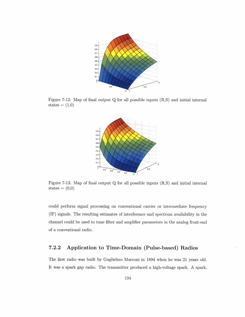
Figure 7-12: Map of final output Q for all possible inputsstates = (1,0)
(R,S) and initial internal
0
-. 2
01
Figure 7-13: Map ofstates = (0,0)
final output Q for all possible inputs (R,S) and initial internal
could perform signal processing on conventional carrier or intermediate frequency
(IF) signals. The resulting estimates of interference and spectrum availability in the
channel could be used to tune filter and amplifier parameters in the analog front-end
of a conventional radio.
7.2.2 Application to Time-Domain (Pulse-based) Radios
The first radio was built by Guglielmo Marconi in 1894 when he was 21 years old.
It was a spark gap radio. The transmitter produced a high-voltage spark. A spark,
194
.5 0.5
0 9
0.7
0.60.5
0.4
0.3
0.2
0.1
1
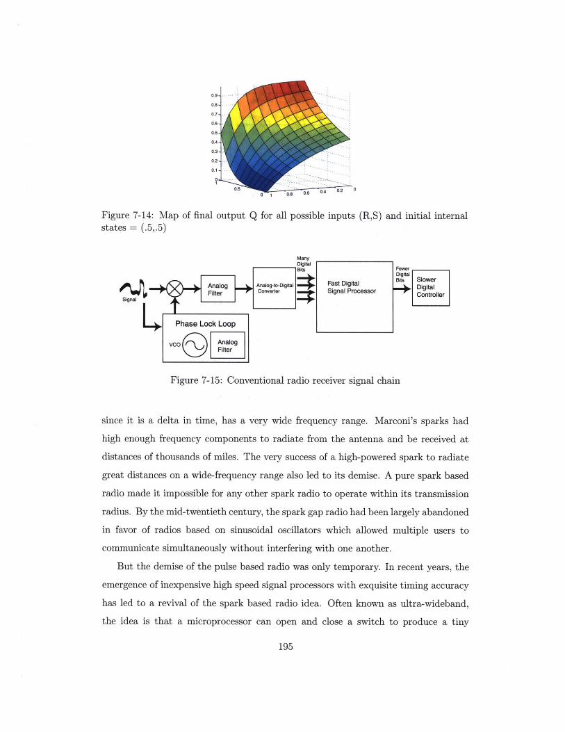
Figure 7-14: Map of final output Q for all possible inputs (R,S) and initial internalstates = (.5,.5)
Many
DigitalBits slow erFast Digital
Analog _ N.Anaog-to-Digitai as DigitalBis So eier Converter Signal Processor ntrller
Phase Lock Loop
Figure 7-15: Conventional radio receiver signal chain
since it is a delta in time, has a very wide frequency range. Marconi's sparks had
high enough frequency components to radiate from the antenna and be received at
distances of thousands of miles. The very success of a high-powered spark to radiate
great distances on a wide-frequency range also led to its demise. A pure spark based
radio made it impossible for any other spark radio to operate within its transmission
radius. By the mid-twentieth century, the spark gap radio had been largely abandoned
in favor of radios based on sinusoidal oscillators which allowed multiple users to
communicate simultaneously without interfering with one another.
But the demise of the pulse based radio was only temporary. In recent years, the
emergence of inexpensive high speed signal processors with exquisite timing accuracy
has led to a revival of the spark based radio idea. Often known as ultra-wideband,
the idea is that a microprocessor can open and close a switch to produce a tiny
195
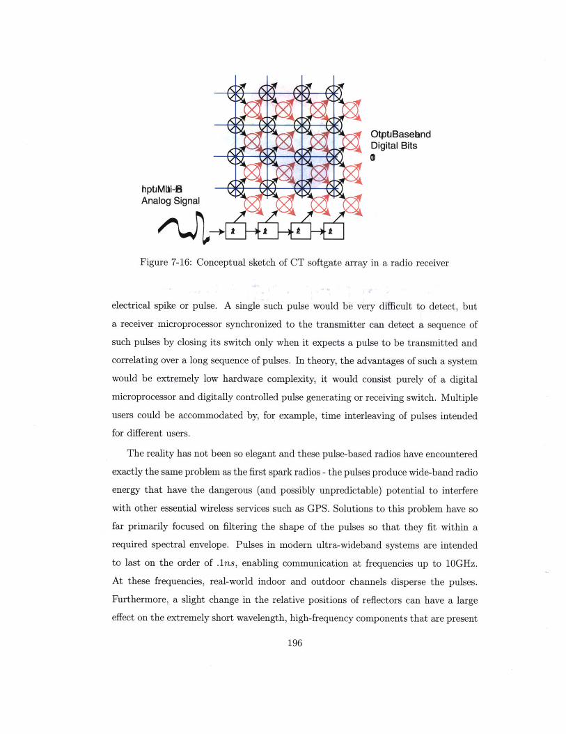
OtptbBaseandDigital Bits
hptiMLi-BAnalog Signal
Figure 7-16: Conceptual sketch of CT softgate array in a radio receiver
electrical spike or pulse. A single such pulse would be very difficult to detect, but
a receiver microprocessor synchronized to the transmitter can detect a sequence of
such pulses by closing its switch only when it expects a pulse to be transmitted and
correlating over a long sequence of pulses. In theory, the advantages of such a system
would be extremely low hardware complexity, it would consist purely of a digital
microprocessor and digitally controlled pulse generating or receiving switch. Multiple
users could be accommodated by, for example, time interleaving of pulses intended
for different users.
The reality has not been so elegant and these pulse-based radios have encountered
exactly the same problem as the first spark radios - the pulses produce wide-band radio
energy that have the dangerous (and possibly unpredictable) potential to interfere
with other essential wireless services such as GPS. Solutions to this problem have so
far primarily focused on filtering the shape of the pulses so that they fit within a
required spectral envelope. Pulses in modern ultra-wideband systems are intended
to last on the order of .1ns, enabling communication at frequencies up to 10GHz.
At these frequencies, real-world indoor and outdoor channels disperse the pulses.
Furthermore, a slight change in the relative positions of reflectors can have a large
effect on the extremely short wavelength, high-frequency components that are present
196
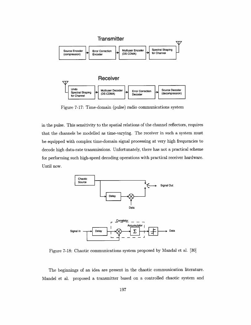
Transmitter
Source Encoder Error Correction Multiuser Encoder Spectral Shaping(compression) Encoder (DS CDMA) for Channel
Receiver
Undocra Sain Multiuser Decoder Error Correction Suc eoe-nd SetaShpn (DS CDMVA) Decoder (decompression)for Channel+(dcmrsin
Figure 7-17: Time-domain (pulse) radio communications system
in the pulse. This sensitivity to the spatial relations of the channel reflectors, requires
that the channels be modelled as time-varying. The receiver in such a system must
be equipped with complex time-domain signal processing at very high frequencies to
decode high data-rate transmissions. Unfortunately, there has not a practical scheme
for performing such high-speed decoding operations with practical receiver hardware.
Until now.
ChaoticSource
Signal Out
-+Delay
Data
Correlator
Accumulator
Signal In o Delay Data
Figure 7-18: Chaotic communications system proposed by Mandal et al. [30]
The beginnings of an idea are present in the chaotic communication literature.
Mandel et al. proposed a transmitter based on a controlled chaotic system and
197
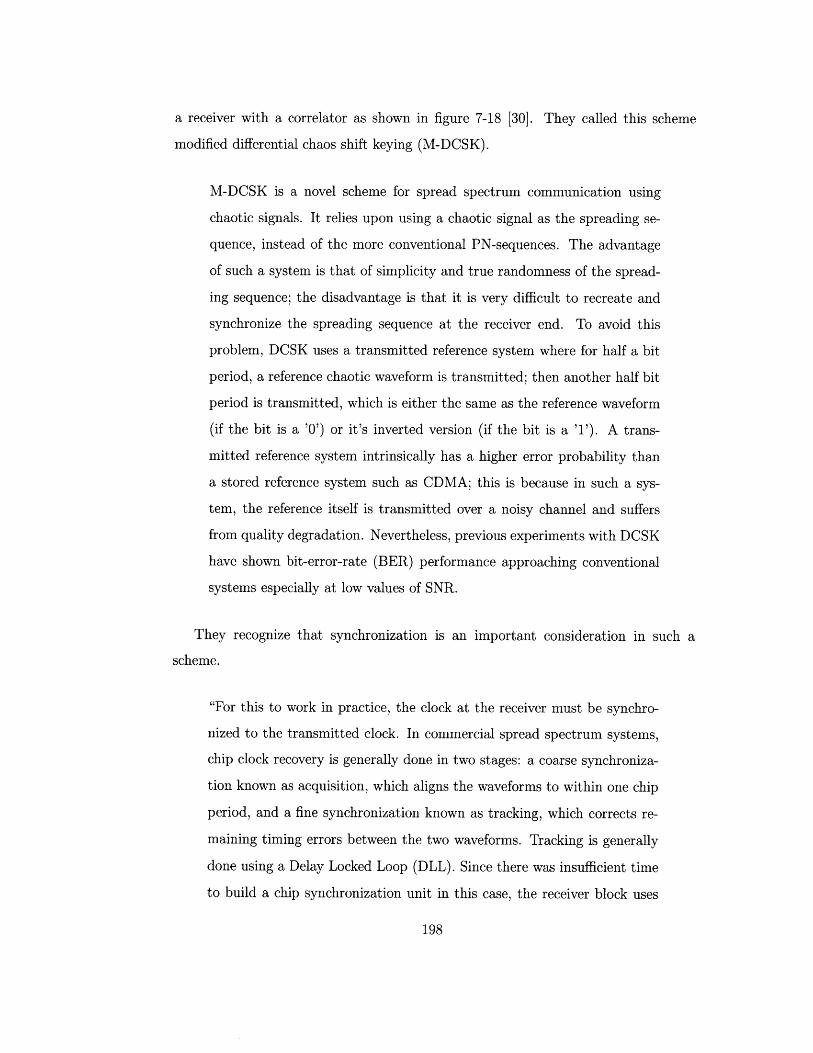
a receiver with a correlator as shown in figure 7-18 [30]. They called this scheme
modified differential chaos shift keying (M-DCSK).
M-DCSK is a novel scheme for spread spectrum communication using
chaotic signals. It relies upon using a chaotic signal as the spreading se-
quence, instead of the more conventional PN-sequences. The advantage
of such a system is that of simplicity and true randomness of the spread-
ing sequence; the disadvantage is that it is very difficult to recreate and
synchronize the spreading sequence at the receiver end. To avoid this
problem, DCSK uses a transmitted reference system where for half a bit
period, a reference chaotic waveform is transmitted; then another half bit
period is transmitted, which is either the same as the reference waveform
(if the bit is a '0') or it's inverted version (if the bit is a '1'). A trans-
mitted reference system intrinsically has a higher error probability than
a stored reference system such as CDMA; this is because in such a sys-
tem, the reference itself is transmitted over a noisy channel and suffers
from quality degradation. Nevertheless, previous experiments with DCSK
have shown bit-error-rate (BER) performance approaching conventional
systems especially at low values of SNR.
They recognize that synchronization is an important consideration in such a
scheme.
"For this to work in practice, the clock at the receiver must be synchro-
nized to the transmitted clock. In commercial spread spectrum systems,
chip clock recovery is generally done in two stages: a coarse synchroniza-
tion known as acquisition, which aligns the waveforms to within one chip
period, and a fine synchronization known as tracking, which corrects re-
maining timing errors between the two waveforms. Tracking is generally
done using a Delay Locked Loop (DLL). Since there was insufficient time
to build a chip synchronization unit in this case, the receiver block uses
198
the same base clock as the transmitter. This is, however, not a major lim-
itation, since the system being built is an experimental/ proof-of-concept
one."
There is actually a deep reason why synchronization and pulse shaping are salient
issues in pulse-based radios. Pulse radios are essentially the Fourier transform of
conventional sinusoidal radios. Therefore the purposes of this discussion, I call pulse-
based radios, time-domain radios, and I call conventional sinusoidal-based radios,
frequency-domain radios. Frequency-domain radios employ a delta in frequency, while
pulse-based time-domain radios employ delta's in time. (DS/CDMA should also be
properly considered time-domain radio, but it uses a pseudo-random bit stream to
produce a wideband frequency spectrum instead of short pulses.) The frequency-time
translation carries over to issues in hardware design. Every difficulty in controlling
frequency in a frequency-domain radio rears its head as a difficulty with control-
ling timing in a time-domain radio. For example, local high-frequency oscillators
with good phase-stability are difficult to build in frequency-domain radios. In time-
domain radios, delay-lines with stable delay-times are challenging to build. Making
good receiver filters to detect particular frequencies translates into requiring good
receiver synchronization to pick out particular instants in time. Making good filters
and designing modulation schemes using oscillators to shape the transmitted spectral
envelope translates into controlling timing and designing sequences which accomplish
this same end in the time domain. Since time-domain signal processing has tradition-
ally been the domain of digital signal processors, time-domain radios have not been
able to overcome these hurdles cost-effectively at high-frequencies. In fact, in the
commercialization of ultra-wideband wireless systems, sinusoidal based radios seem
poised to win yet again. The technology presented in this dissertation, however, seems
uniquely suited to solve precisely the problem of high-speed low-power analog circuits
for time-domain statistical signal processing.
199

200
Chapter 8
Biographies
8.1 Anantha P. Chandrakasan, MIT EECS, Cam-bridge, MA
Anantha P. Chandrakasan received B.S, M.S. and Ph.D. degrees in Electrical Engi-neering and Computer Sciences from the University of California, Berkeley, in 1989,1990, and 1994 respectively. Since September 1994, he has been at the MassachusettsInstitute of Technology, Cambridge, and is currently an Associate Professor of Elec-trical Engineering and Computer Science. He held the Analog Devices Career Devel-opment Chair from 1994 to 1997. He received the NSF Career Development award in1995, the IBM Faculty Development award in 1995 and the National SemiconductorFaculty Development award in 1996 and 1997. He is a Co-founder and Chief Scientistat Engim, a company focused on high-performance wireless communications.
He has received several best paper awards including the 1993 IEEE Communica-tions Society's Best Tutorial Paper Award, the IEEE Electron Devices Society's 1997Paul Rappaport Award for the Best Paper in an EDS publication during 1997 andthe 1999 Design Automation Conference Design Contest Award.
His research interests include the ultra low power implementation of custom andprogrammable digital signal processors, distributed wireless sensors, multimedia de-vices, emerging technologies, and CAD tools for VLSI. He is a co-author "Low PowerDigital CMOS Design" by Kluwer Academic Publishers and "Digital Integrated Cir-cuits" (second edition) by Prentice-Hall. He is also a co-editor of "Low Power CMOSDesign" and "Design of High-Performance Microprocessor Circuits" from IEEE press.
He has served on the technical program committee of various conferences includingISSCC, VLSI Circuits Symposium, DAC, and ISLPED. He has served as a technicalprogram co-chair for the 1997 International Symposium on Low-power Electronicsand Design (ISLPED), VLSI Design '98, and the 1998 IEEE Workshop on SignalProcessing Systems, and as a general co-chair of the 1998 ISLPED. He was an as-sociate editor for the IEEE Journal of Solid-State Circuits from 1998 to 2001. He
201
served as an elected member of the Design and Implementation of Signal ProcessingSystems (DISPS) Technical Committee of the Signal Processing Society and serveson the SSCS AdCOM. He was the Signal Processing Sub-committee chair for ISSCC1999 through 2001, the program vice-chair for ISSCC 2002, the technical programchair for ISSCC 2003.
8.2 Hans-Andrea Loeliger, ETH, Zurich, Switzer-land
Hans-Andrea Loeliger has been full Professor of Signal Processing at the Signal Pro-cessing Laboratory of ETH Zurich since June 2000. He studied Electrical Engineeringat ETH Zurich, and there he also received the Ph.D. degree in 1992. He then joinedLinkping University, Sweden, as assistant professor ("forskarassistent"). In 1995,he returned to Switzerland and (together with Felix Tarky) founded the consultingcompany Endora Tech AG, Basel, with which he remained until his return to ETH.
His research focuses on error correcting codes and coded modulation, modellingand analysis of signals and systems, and robust nonlinear analog computation net-works. His research interests include Information theory and its applications incommunications and signal processing Error correcting codes and coded modula-tion schemes Digital signal processing in communications, acoustics, and other fieldsGraphical models ("factor graphs") for coding and signal processing Signal processingwith robust nonlinear analog networks ("analog decoder").
8.3 Jonathan Yedidia, Mitsubishi Electronics Re-search Lab, Cambridge, MA
Jonathan Yedidia's graduate work at Princeton (1985-1990) and post-doctoral workat Harvard's Society of Fellows (1990-1993) focused on theoretical condensed-matterphysics, particularly the statistical mechanics of systems with quenched disorder.From 1993 to 1997, he was a professional chess player and teacher. He then workedat the internet startup company Viaweb, where he helped develop the shopping searchengine that has since become Yahoo's shopping service. In 1998, Dr. Yedidia joinedthe Mitsubishi Electric Research Laboratory (MERL)Cambridge Research Labora-tory. He is particularly interested in the development of new methods to analyzegraphical models. His work has applications in the fields of artificial intelligence,digital communications, and statistical physics.
Most of Yedidia's current research involves the application of statistical methodsto "inference" problems. Some important fields which are dominated by the issue ofinference are computer vision, speech recognition, natural language processing, error-correction, and diagnosis. Essentially, any time you are receiving a noisy signal, andneed to infer what is really out there, you are dealing with an inference problem. Aproductive way to deal with an inference problem is to formalize it as a problem of
202
computing probabilities in a graphical model. Graphical models, which are referred toin various guises as "Markov random fields," "Bayesian networks," or "factor graphs,"provide a statistical framework to encapsulate our knowledge of a system and to inferfrom incomplete information.
Physicists who use the techniques of statistical mechanics to study the behavior ofdisordered magnetic spin systems are actually studying a mathematically equivalentproblem to the inference problem studied by computer scientists, but with differentterminology, goals, and perspectives. Yedidia's own research has focused on the sur-prising relationships between methods that are used in the two communities, and onpowerful new techniques and algorithms that exploit those relationships. A majorcurrent project involves analyzing and designing error-correcting codes using gener-alized belief propagation algorithms.
8.4 Neil Gershenfeld, MIT Media Lab, Cambridge,MA
Professor Neil Gershenfeld is the Director of MIT's Center for Bits and Atoms, aninterdisciplinary initiative that is broally exploring how the content of informationrelates to its physical representation, from atomic nuclei to global networks. CBA'sintellectual community and research resources cut across traditional divisions of in-quiry by disciplines and length scales in order to bring together the best features of thebits of new digital worlds with the atoms of the physical world. Dr. Gershenfeld hasalso led the Media Lab's Things That Think industrial research consortium, whichpioneered moving computation out of conventional computers and into the rest of theworld, and works with the Media Lab Asia on coordinating the technical guidancefor this ambitious international effort based in India that is investigating technol-ogy for global development. His own laboratory studies fundamental mechanismsfor manipulating information (which led to the development of molecular logic usedto implement the first complete quantum computation and to analog circuits thatcan efficiently perform optimal digital operations), the integration of these ideas intoeveryday objects such as furniture (seen in the Museum of Modern Art and used inautomobile safety systems), and applications with partners ranging from developinga computerized cello for Yo-Yo Ma and stage for the Flying Karamazov Brothers toinstrumentation used by rural Indian villagers and nomadic reindeer herders. Beyondhis many technical publications and patents, he is the author of best-selling booksincluding "When Things Start To Think" and the texts "The Nature of Mathemat-ical Modelling" and "The Physics of Information Technology." His work has beenfeatured by the White House and Smithsonian Institution in their Millennium cele-brations, and been the subject of print, radio, and TV programs in media includingthe New York Times, The Economist CNN, and PBS.
Dr. Gershenfeld has a B.A. in Physics with High Honors from Swarthmore College,was a member of the research staff at Bell Labs where he studied laser interactionswith atomic and nuclear systems, received a Ph.D. in Applied Physics from Cornell
203
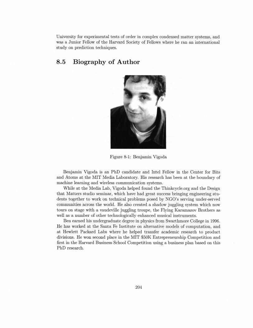
University for experimental tests of order in complex condensed matter systems, andwas a Junior Fellow of the Harvard Society of Fellows where he ran an internationalstudy on prediction techniques.
8.5 Biography of Author
Figure 8-1: Benjamin Vigoda
Benjamin Vigoda is an PhD candidate and Intel Fellow in the Center for Bitsand Atoms at the MIT Media Laboratory. His research has been at the boundary ofmachine learning and wireless communication systems.
While at the Media Lab, Vigoda helped found the Thinkcycle.org and the Designthat Matters studio seminar, which have had great success bringing engineering stu-dents together to work on technical problems posed by NGO's serving under-servedcommunities across the world. He also created a shadow juggling system which nowtours on stage with a vaudeville juggling troupe, the Flying Karamazov Brothers aswell as a number of other technologically enhanced musical instruments.
Ben earned his undergraduate degree in physics from Swarthmore College in 1996.He has worked at the Santa Fe Institute on alternative models of computation, andat Hewlett Packard Labs where he helped transfer academic research to productdivisions. He won second place in the MIT $50K Entrepreneurship Competition andfirst in the Harvard Business School Competition using a business plan based on thisPhD research.
204
Bibliography
[1] K. Abend and B. D. Fritchman (May 1970). Statistical Detection for Communi-cation channels with intersymbol interference. Proc. IEEE, vol. 58, pp. 779-785
[2] P. Bardell, W. McAnney, and S. Jacob (1987). Built-In Test for VLSI: Pseudo-random Techniques. New York, NY: John Wiley and Sons.
[3] S. E. Bensley and B. Aazhang (1998). Maximum Likelihood Synchronization ofa Single User for Code Division Multiple Access Communication Systems. IEEETransactions on Communications, COM-46, no. 3, pp. 392-399
[4] Rafael J. Betancourt-Zamora, Shwetabh Verma and Thomas H. Lee (2001). 1-GHzand 2.8-GHz CMOS Injection-locked Ring Oscillator Prescalers. 2001 Symposiumon VLSI Circuits, Kyoto, Japan, June 14, 2001, pp. 47-50
[5] G. Cauwenberghs (1995). Micropower CMOS Algorithmic A/D/A Converter.IEEE Transactions on Circuits and Systems I: Fundamental Theory and Applica-tions, Vol. 42, No. 11, pp. 913-919
[6] H. C. Casey, Jr. (May 1998). Supplemental Chapter to Introduction to Siliconand III-V Compound Semiconductor Devices for Integrated Circuits. Departmentof Electrical and Computer Engineering Duke University
[7] K. M. Cuomo and Alan V. Oppenheim (Jul. 1993). Circuit Implementation ofSynchronized Chaos with Applications to Communications. Physical Review Let-ters, 1993, Vol. 71, No. 1.
[8] Jie Dai (Aug. 2002). Doctoral Dissertation: Design Methodology for Analog VLSIImplementations of Error COntrol Decoders. Salt Lake City, Utah: University ofUtah.
[9] A. S. Dmitriev, A. I. Panas, S. 0. Starkov (Oct. 2001). Direct Chaotic Commu-nication in Microwave Band.
[10] Andreas Demosthenous and John Taylor (Feb. 2001). A 10OMb/s, 2.8V CMOSCurrent-Mode Analogue Viterbi Decoder. IEEE Trans. Inform. Theory, vol. 47,pp. 520-548
205
[11] Jose E. Franca and Yannis Tsividis (1994). Design of Analog-Digital VLSI CIr-cuits for Telecommunications and Signal Processing, second ed. Englewood Cliffs,NJ: Prentice Hall.
[12] M.A. Franklin and T. Pan (Nov. 1994). Performance Comparison of Asyn-chronous Adders. Proceedings of the International Symposium on Advanced Re-search in Asynchronous Circuits and Systems, 1994, pp. 117-125
[13] G. D. Forney (Feb. 2001). Codes on Graphs: Normal Realizations. IEEE Trans.Inform. Theory, vol. 47, pp. 520-548
[14] Neil Gershenfeld and Geoff Grinstein (1995). Entrainment and Communicationwith Dissipative Pseudorandom Dynamics. Physical Review Letters, 74, pp. 5024
[15] Neil Gershenfeld (1999). The Nature of Mathematical Modeling. Cambridge, UK:Cambridge University Press.
[16] T. R. Giallorenzi and S.G. Wilson (Sept. 1996). Suboptimum Multiuser Receiversfor Convolutionally Coded Asynchronous DS-CDMA Systems. IEEE Transactionson Communications, 44, pp. 1183-1196
[17] M.R. Greenstreet and P. Cahoon (Nov. 1994). How Fast Will the Flip Flop? Pro-ceedings of the International Symposium on Advanced Research in AsynchronousCircuits and Systems, 1994, pp. 77-86
[18] David J. Griffiths (1995). Introduction to Quantum Mechanics. Upper SaddleRiver, NJ: Prentice Hall.
[19] J. Hagenauer (Feb. 1998). Decoding of Binary Codes with Analog Networks.Proc. 1998 Information Theory Workshop, San Diego, CA, Feb. 811, pp. 1314.
[20] J. Hagenauer and M. Winklhofer (Feb. 1998). The Analog Decoder. Proc. 1998IEEE Int. Symp. on Information Theory, Cambridge, MA USA, Aug. 1621, p. 145.
[21] Gunhee Han and Edgar Sanchez-Sinencio (Dec. 1998). CMOS TransconductanceMultipliers: A Tutorial. IEEE Transactions on Circuits and Systems II: Analogand Digital signal Processing, VOL.45, NO.12
[22] Tom Heskes (2002). Stable fixed points of belief propagation are minima of theBethe free energy. Proceedings of Neural Information Processing, 2002
[23] Erika Jonietz (Dec. 2001). Community-Owned Wireless Networks Are GainingPopularity and Could Help Bridge the Digital Divide. Innovation: Unwiring theWeb Technology Review, December 2001
[24] Tobias Koch. Advisor: Justin Dauwels, Matthias Frey and Patrick Merkli incollaboration with Benjamin Vigoda (Feb. 2003). Continuous-Time Synchroniza-tion. Zurich, Switzerland. Semester Project at Institute for Signals and Information(ISI), ETH.
206
[25] Ed. H. S. Leff and A. F. Rex (Jan. 1990) Maxwell's Demon: Entropy, Informa-tion, Computing Washington State, USA: Institute of Physics Publishing.
[26] H. Li (Mar. 2001). Building a Dictionary for DNA: Decoding the RegulatoryRegions of a Genome. Institute for Theoretical Physics (ITP) Program on StatisticalPhysics and Biological Information
[27] Douglas Lind and Brian Marcus (Dec. 1995). An Introduction to Symbolic Dy-namics and Coding. New York, NY: Cambridge University Press
[28] Frank R. Kschischang, Brendan J. Frey and Hans-Andrea Loeliger (Feb. 2001).Factor Graphs and the Sum-Product Algorithm. IEEE Transactions on Informa-tion Theory, 47:2, pp. 498-519
[29] Felix Lustenberger (Nov. 2000) Doctoral Dissertation: On the Design of AnalogVLSI Iterative Decoders Zurich, Switzerland: Swiss Federal Institute of Technology(ETH).
[30] Soumyajit Mandal and Soumitro Banerjee (2003). Analysis and CMOS Im-plementation Of A Chaos-based Communication System. IEEE Transactions onCircuits and Systems I,
[31] G. J. Minty. (1957). A Comment on the Shortest-Route Problem. OperationalResearch, vol. 5, p. 724
[32] Andreas F. Molisch (2001). Wideband Wireless Digital Communications. UpperSaddle River, NJ: Prentice-Hall
[33] S.V. Morton, S.S. Appleton, and M.J. Liebelt (Nov. 1994). An Event ControlledReconfigurable Multi-Chip FFT. Proceedings of the International Symposium onAdvanced Research in Asynchronous Circuits and Systems, 1994, pp. 144-153
[34] Jan Mulder, Wouter Serdijn, Albert C. van der Woerd, Arthur H.M. van Roer-mund (1999). Dynamic Translinear and Log-Domain Circuits. Boston, Ma: KluwerPress
[35] Alison Payne,Apinunt Thanachayanont, and C.Papavassilliou (Sept. 1998). A150-MHz Translinear Phase-Locked Loop. IEEE Transactions on Circuits andSystems II:Analog and Digital signal Processing, Vol.45, No.9
[36] L. M. Pecora and T. L. Caroll (1990). Synchronization in Chaotic Systems.Physical Review Letters, vol. 64, pp. 821-824
[37] John G. Proakis (2001). Digital Communications. Boston, MA: McGraw-Hill
[38] L. R. Rabiner and B. H. Juang (Jan. 1986). An Introduction to Hidden MarkovModels. IEEE ASSP Magazine, pp. 4-15
207
[39] Mark C. Reed (Oct. 1999) Doctoral Dissertation: Iterative Receiver Techniquesfor Coded Multiple Access Communication Systems School of Physics and Elec-tronics Systems Engineering, University of South Australia.
[40] P. V. Rooyen, M. Lotter, D. v. Wyk. (2000). Space-Time Processing for CDMAMobile Communications. Norwell, MA: Kluwer Academic Publishers.
[41] Rahul Sarpeshkar. (Apr. 1997) Doctoral Dissertation: Efficient Precise Compu-tation with Noisy Components: Extrapolating From an Electronic Cochlea to theBrain Pasadena, CA: California Institute of Technology (CalTech).
[42] Evert Seevinck (1999). Analysis and Synthesis of Translinear Integrated Circuits.Amsterdam, Netherlands: Elsevier Press
[43] M.H. Shakiba, D.A. Johns and K.W. Martin. (Dec. 1998). BiCMOS Circuits forAnalog Viterbi Decoders. IEEE Trans. on Circuits and Systems - II: Analog andDigital Signal Processing, VOL.45, pp. 1527-1537.
[44] S. Sheng and R. Brodersen. (1998). Low-Power CMOS Wireless Communica-tions: A Wideband CDMA System Design. Boston, MA: Kluwer Academic Pub-lishers.
[45] Semiconductor Industry Association. (2002). International Technology Roadmapfor Semiconductors, 2001. SEMATECH http://public.itrs.net/Reports.htm
[46] A.C. Singer and A.V. Oppenheim. (1999). Circuit Implementations of SolitonSystems. International Journal of Bifurcation and Chaos, Vol. 9, No. 4, pp. 571-590.
[47] Robert H. Walden.(Feb. 1999). Performance Trends for Analog-to-Digital Con-verters. IEEE Communications Magazine, pp. 96-101
[48] Remco J. Wiegerink (1993). Analysis and Synthesis of MOS Translinear Circuits.Boston, Ma: Kluwer Press
[49] Sergio Verd. (Jan. 1986). Minimum Probability of Error for Asynchronous Gaus-sian Multiple Access Channels. IEEE Trans. on Info. Theory, pp. 85-96
[50] Sergio Verd. (Jan. 1989). Computational Complexity of Optimum MultiuserDetection. Algorithmica Vol. 4, No. 3, pp. 303-312
[51] Sergio Verd (1998). Multiuser Detection. New York, NY: Cambridge UniversityPress
[52] Benjamin Vigoda, Justin Dauwels, Neil Gershenfeld, and Hans-Andrea Loeliger.(In Press). Low-Complexity LFSR Synchronization by Forward-Only Message Pass-ing. Submitted to IEEE Transaction on Information Theory
[53] A.J. Viterbi (1995). CDMA, Principles of Spread Spectrum Communication.Reading, MA: Addison-Wesley Longman Inc.
208
[54] Glenn Watanabe, Henry Lau and Juergen Schoepf. (Aug. 2000). Integrated MixerDesign. Proceedings of the Second IEEE Asia-Pacific Conference on ASIC
[55] J. S. Yedidia, W. T.Freeman and Y. Weiss. (2001). Understanding Belief Prop-agation and Its Generalizations. published as chapter 8 of 'Exploring ArtificialIntelligence in the New Millennium eds. G. Lakemeyer and B. Nebel, pp. 239-269,Morgan Kaufmann 2003
[56] J. S. Yedidia, W. T.Freeman and Y. Weiss. (Apr. 2002). Constructing FreeEnergy Approximations and Generalized Belief Propagation Algorithms.
209
Related Documents