73 wileyonlinelibrary.com © 2012 Wiley-VCH Verlag GmbH & Co. KGaA, Weinheim small 2012, 8, No. 1, 73–79 Organic Transistors DOI: 10.1002/smll.201101677 Contact Resistance and Megahertz Operation of Aggressively Scaled Organic Transistors Frederik Ante, Daniel Kälblein, Tarek Zaki, Ute Zschieschang, Kazuo Takimiya, Masaaki Ikeda, Tsuyoshi Sekitani, Takao Someya, Joachim N. Burghartz, Klaus Kern, and Hagen Klauk* Organic thin-film transistors (TFTs) are of interest for large-area electronics applications, such as conformable sensor arrays and flexible active-matrix displays, in which the TFTs will typically operate at frequencies below about 100 kHz. [1–5] For more demanding applications, such as high-resolution video displays with integrated row and column drivers, TFTs capable of operating at frequencies up to about 10 MHz will be required. The cutoff frequency f T of a field-effect transistor is often calculated using Equation (1): [6] f T ≈ µ eff V V GS − th 2 π LL L + 2 C ( ( ) ) (1) with the effective charge-carrier mobility μ eff , the gate–source voltage V GS , the threshold voltage V th , the channel length L, and the contact length L C . The contact length L C is the distance by which the gate electrode overlaps the source and drain contacts (see Figure 1a). The reason why L C appears in Equation (1) is that this overlap creates a para- sitic capacitance that is charged and discharged during each switching event. Intuitively, the contact length L C should therefore be minimized to achieve the highest possible cutoff frequency. [7,8] Equation (1) suggests that for an effective mobility of 1 cm 2 (V s) −1 and lateral dimensions (L, L C ) of 1 μm, a cutoff frequency of 10 MHz can be achieved at a voltage of 3 V (or a frequency of 100 MHz at 30 V). Effective mobilities around 1 cm 2 (V s) −1 are indeed commonly measured in organic TFTs, but usually only if the channel length is much larger than 1 μm. [9–11] When the channel length is reduced to about 1 μm, the channel resistance R channel becomes smaller than the contact resistance R C , thus causing the effective mobility μ eff of the transistor to drop substantially below the intrinsic mobility μ 0 of the semiconductor: [12,13] µ eff ≈ µ 0 1 − µ 0 Ci WR C ( ( V GS − V th ) ) L + µ 0 CiWR C V GS −V th 2 (2) with the gate-dielectric capacitance per unit area C i and the channel width W. This is why the effective mobility μ eff in TFTs with aggressively reduced dimensions is usually below 1 cm 2 (V s) −1 , even if the semiconductor is known to have a much larger intrinsic mobility μ 0 . This is also why cutoff frequencies reported for organic TFTs rarely exceed 1 MHz. [7,8,14,15] A record cutoff frequency of 28 MHz meas- ured at a relatively high voltage of 25 V has been reported for TFTs based on the fullerene C 60 having a channel length of 2 μm. [16] TFTs based on C 60 as the semiconductor can have large effective mobilities (2.2 cm 2 (V s) −1 in Reference [16]), but they cannot be operated in air. The above-mentioned influence of the channel length on the effective mobility and on the cutoff frequency of organic TFTs has been studied in great detail. [12] Most of these studies employed TFTs with the coplanar structure, since in this architecture the source and drain contacts are fabricated prior to the deposition of the organic semicon- ductor layer and thus can be patterned with high resolution Dr. F. Ante, Dr. D. Kälblein, Dr. U. Zschieschang, Prof. K. Kern, Dr. H. Klauk Max Planck Institute for Solid State Research Heisenbergstr. 1, 70569 Stuttgart, Germany E-mail: [email protected] T. Zaki, Prof. J. N. Burghartz Institut für Mikroelektronik/IMS CHIPS Allmandring 30a, 70569 Stuttgart, Germany Prof. K. Takimiya Department of Applied Chemistry Graduate School of Engineering Institute for Advanced Materials Research Hiroshima University Higashi-Hiroshima, Japan Dr. M. Ikeda Functional Chemicals R&D Laboratories Nippon Kayaku Co., Ltd., Kita-ku, Tokyo, Japan Prof. T. Sekitani, Prof. T. Someya Department of Electrical Engineering University of Tokyo Tokyo, Japan Prof. K. Kern Institut de Physique de la Matière Condensée École Polytechnique Fédérale de Lausanne 1015 Lausanne, Switzerland

Welcome message from author
This document is posted to help you gain knowledge. Please leave a comment to let me know what you think about it! Share it to your friends and learn new things together.
Transcript
Organic Transistors
Contact Resistance and Megahertz Operation of Aggressively Scaled Organic Transistors
Frederik Ante, Daniel Kälblein, Tarek Zaki, Ute Zschieschang, Kazuo Takimiya, Masaaki Ikeda, Tsuyoshi Sekitani, Takao Someya, Joachim N. Burghartz, Klaus Kern, and Hagen Klauk*
Organic thin-film transistors (TFTs) are of interest for large-area electronics applications, such as conformable sensor arrays and flexible active-matrix displays, in which the TFTs will typically operate at frequencies below about 100 kHz.[1–5] For more demanding applications, such as high-resolution video displays with integrated row and column drivers, TFTs capable of operating at frequencies up to about 10 MHz will be required. The cutoff frequency fT of a field-effect transistor is often calculated using Equation (1):[6]
fT ≈µeff V VGS− th
2π L L L+ 2 C((
))
(1)
with the effective charge-carrier mobility μeff, the gate–source voltage VGS, the threshold voltage Vth, the channel length L, and the contact length LC. The contact length LC is the distance by which the gate electrode overlaps the source and drain contacts (see Figure 1a). The reason why LC appears in Equation (1) is that this overlap creates a para-sitic capacitance that is charged and discharged during each switching event. Intuitively, the contact length LC should therefore be minimized to achieve the highest possible cutoff frequency.[7,8]
Equation (1) suggests that for an effective mobility of 1 cm2 (V s)−1 and lateral dimensions (L, LC) of 1 μm, a cutoff frequency of 10 MHz can be achieved at a voltage of 3 V (or a frequency of 100 MHz at 30 V). Effective mobilities around 1 cm2 (V s)−1 are indeed commonly measured in organic
© 2012 Wiley-VCH Verlag Gmbsmall 2012, 8, No. 1, 73–79
DOI: 10.1002/smll.201101677
Dr. F. Ante, Dr. D. Kälblein, Dr. U. Zschieschang, Prof. K. Kern, Dr. H. KlaukMax Planck Institute for Solid State Research Heisenbergstr. 1, 70569 Stuttgart, Germany E-mail: [email protected]
T. Zaki, Prof. J. N. BurghartzInstitut für Mikroelektronik/IMS CHIPS Allmandring 30a, 70569 Stuttgart, Germany
Prof. K. TakimiyaDepartment of Applied Chemistry Graduate School of Engineering Institute for Advanced Materials Research Hiroshima University Higashi-Hiroshima, Japan
TFTs, but usually only if the channel length is much larger than 1 μm.[9–11] When the channel length is reduced to about 1 μm, the channel resistance Rchannel becomes smaller than the contact resistance RC, thus causing the effective mobility μeff of the transistor to drop substantially below the intrinsic mobility μ0 of the semiconductor:[12,13]
µeff ≈ µ0
1−
µ0CiWRC (
(VGS−Vth)
)L + µ0CiWRC VGS−Vth
2
(2)
with the gate-dielectric capacitance per unit area Ci and the channel width W. This is why the effective mobility μeff in TFTs with aggressively reduced dimensions is usually below 1 cm2 (V s)−1, even if the semiconductor is known to have a much larger intrinsic mobility μ0. This is also why cutoff frequencies reported for organic TFTs rarely exceed 1 MHz.[7,8,14,15] A record cutoff frequency of 28 MHz meas-ured at a relatively high voltage of 25 V has been reported for TFTs based on the fullerene C60 having a channel length of 2 μm.[16] TFTs based on C60 as the semiconductor can have large effective mobilities (2.2 cm2 (V s)−1 in Reference [16]), but they cannot be operated in air.
The above-mentioned influence of the channel length on the effective mobility and on the cutoff frequency of organic TFTs has been studied in great detail.[12] Most of these studies employed TFTs with the coplanar structure, since in this architecture the source and drain contacts are fabricated prior to the deposition of the organic semicon-ductor layer and thus can be patterned with high resolution
73wileyonlinelibrary.comH & Co. KGaA, Weinheim
Dr. M. IkedaFunctional Chemicals R&D Laboratories Nippon Kayaku Co., Ltd., Kita-ku, Tokyo, Japan
Prof. T. Sekitani, Prof. T. SomeyaDepartment of Electrical Engineering University of Tokyo Tokyo, Japan
Prof. K. KernInstitut de Physique de la Matière Condensée École Polytechnique Fédérale de Lausanne 1015 Lausanne, Switzerland
F. Ante et al.
74
communications
Figure 1. a) Schematic cross section illustrating the inverted staggered (bottom-gate, top-contact) organic TFT structure. The extent of the channel length L and of the contact length LC as well as the structure of the gate dielectric are indicated. b) Photograph showing a dinaphtho[2,3-b:2′,3′-f]thieno[3,2-b]thiophene (DNTT) TFT with a channel length of 1 μm and a contact length of 2 μm manufactured using silicon stencil masks. c) Scanning electron microscopy (SEM) image depicting the well-defined channel length of 1 μm and the smooth contact edges. SAM = self-assembled monolayer.
by photolithography or electron-beam lithography. How-ever, experiments[12] and simulations[17] show that coplanar organic TFTs often have a large contact resistance, since the gate field is partially shielded by the source and drain contacts and a channel is thus induced only in the region between the contacts. As a result, in coplanar organic TFTs the efficient charge transfer between the contacts and the semiconductor is limited to the narrow regions where the gate-induced channel touches the contact edges.[17] In stag-gered TFTs the source and drain contacts are located oppo-site the gate dielectric, so the channel extends beyond the contact edges along the entire contact length LC. As a result, in staggered TFTs the area available for charge transfer is much larger than in coplanar TFTs,[17] which explains why staggered organic TFTs often have a smaller contact resist-ance than coplanar organic TFTs.[12]
An important question arising from these considera-tions is to what extent the contact length LC affects the con-tact resistance RC in staggered organic TFTs. In all previous studies on the contact resistance of staggered organic TFTs the contact length LC was very large (tens of micrometers), so that the influence of LC on RC was insignificant.[12,18,19] The fact that the contact resistance and the effective mobility of staggered TFTs are indeed affected when the contact length LC is reduced is already known from transistors based on amorphous silicon,[20] microcrystalline silicon,[21] carbon nan-otubes,[22] silicon nanowires,[23] and graphene.[24]
Herein, we provide a rigorous analysis of the complex relationships between contact length, contact resistance, and effective mobility in aggressively scaled staggered organic TFTs. We also show that achieving a high cutoff frequency in staggered organic TFTs is not as simple as minimizing L and LC, as Equation (1) would suggest. For this study we fab-ricated staggered (bottom-gate, top-contact) TFTs based on the air-stable organic semiconductor dinaphtho[2,3-b:2′,3′-f]
www.small-journal.com © 2012 Wiley-VCH Verlag GmbH & Co. KGaA
thieno[3,2-b]thiophene (DNTT) with channel lengths L ranging from 60 to 1 μm and well-defined contact lengths LC of 200, 20, 5, and 2 μm. To realize top-contact organic TFTs with such small dimensions without exposing the semiconductor layer to potentially harmful organic solvents during photolithography or electron-beam lithography,[25] we took advantage of high-resolution silicon stencil masks (see Figure S1, Supporting Information).[26–30]
To fabricate fully patterned TFTs, a set of four stencil masks is required. The first mask is used to define the gate elec-trodes, which consist of 30-nm-thick alu-minum deposited by thermal evaporation in vacuum. With the second mask, small areas on the aluminum required for elec-trical probing are covered with 20-nm-thick gold to prevent the formation of an insulating layer in these areas. The gate dielectric is a combination of 3.6-nm-thick plasma-grown AIOx and a 1.7-nm-thick tetradecylphosphonic acid self-assembled
monolayer (SAM) and has a capacitance per unit area (Ci) of 800 nF cm−2.[31] Through the third stencil mask a 25-nm-thick layer of the organic semiconductor DNTT is deposited by sublimation in vacuum.[9,31,32] Finally, 25-nm-thick gold source and drain contacts are deposited by thermal evapo-ration through the fourth stencil mask. The schematic cross section and a photo graph of a completed transistor with a channel length of 1 μm and a contact length of 2 μm are shown in Figure 1b. The SEM image in Figure 1c depicts the sharp contact edges of a TFT with a channel length of 1 μm. The atomic force microscopy (AFM) image in Figure S2 highlights the well-defined overlaps between the gate elec-trode and the source and drain contacts that can be achieved by stencil-mask patterning. All electrical measurements were performed in ambient air at room temperature.
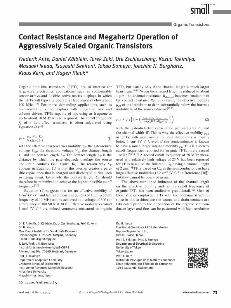
The electrical characteristics of a DNTT TFT with a large channel length (L = 60 μm) and large contact length (LC = 200 μm) are shown in Figure 2. From the transfer characteris-tics of this DNTT TFT, an effective mobility of 2.4 cm2 (V s)−1 is extracted in both the saturation and the linear region. This effective mobility is close to the intrinsic mobility of 3 cm2 (V s)−1 which we have calculated by applying the transmis-sion line method (TLM)[12,32] to a set of DNTT TFTs with channel lengths ranging from 60 to 1 μm and a contact length of 200 μm. The TLM analysis also indicates that these TFTs have a relatively small width-normalized contact resistance of 0.6 kΩ cm (see Figure S3).
When the channel length is reduced, the relative con-tribution of the contact resistance to the total device resist-ance increases and, thus, the effective mobility decreases. For example, the DNTT TFT in Figure S4, which has a small channel length (1 μm) and a large contact length (200 μm), has an effective mobility that is notably smaller than the intrinsic mobility (0.4 cm2 (V s)−1 in the saturation region, 0.2 cm2 (V s)−1 in the linear region). The effective mobilities
, Weinheim small 2012, 8, No. 1, 73–79
Contact Resistance and Megahertz Operation of Organic Transistors
Figure 2. Transfer and output characteristics of a DNTT TFT with relaxed dimensions. The transistor has a channel length of 60 μm and a contact length of 200 μm. From the transfer characteristics, effective mobilities of 2.4 cm2 (V s)−1 (both in the saturation region and in the linear region), an on/off current ratio of 106, a subthreshold swing of 100 mV decade−1, and a threshold voltage of –1.4 V are extracted.
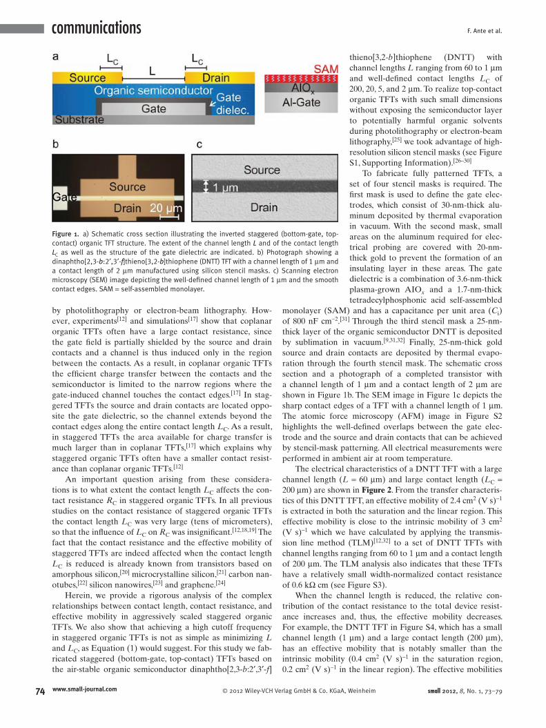
of a set of DNTT TFTs with channel lengths ranging from 60 to 1 μm and a contact length of 200 μm are summarized in Figure S5. As can be seen, both the saturation mobility and the linear mobility decrease significantly with decreasing channel length. This effect is somewhat less pronounced in the saturation region than in the linear region, presumably because the contribution of the contact resistance to the total device resistance is somewhat smaller when the channel near the drain contact is pinched off.[33] The excellent parameter uniformity of DNTT TFTs with channel lengths between 1 and 5 μm fabricated using high-resolution silicon stencil masks is demonstrated in Figure 3.
From the TLM analysis in Figure S3 we can also extract the transfer length LT, which is the characteristic length over which 63% of the charge-carrier exchange between the contacts and the semiconductor occurs.[34] For our DNTT TFTs this transfer length is 10 μm, which is in good agree-ment with previous reports on the transfer length in organic TFTs.[12,18,19,30,35] Figure 4 shows that the output characteris-tics of the DNTT TFTs change dramatically when the con-tact length LC is reduced from a value much larger than the transfer length LT (Figure 4a; LC = 200 μm) to a value similar to or smaller than the transfer length LT (Figure 4b–d; LC = 20, 5, 2 μm). As can be seen, the undesirable nonlinearity of the drain current at small drain–source voltages becomes
© 2012 Wiley-VCH Verlag Gmbsmall 2012, 8, No. 1, 73–79
Figure 3. Transfer characteristics of 47 DNTT TFTs with channel lengths of 1TFTs have a contact length of 20 μm.
more and more pronounced as the contact length LC is reduced below the transfer length LT. At the same time, the effective mobility (both in the saturation region and in the linear region) decreases with decreasing contact length (see Figure 4e). These observations indicate that reducing the con-tact length LC below the transfer length LT causes the contact resistance to increase considerably.
To analyze the relationship between the transfer length, the contact length, and the contact resistance, we applied the TLM method to sets of DNTT TFTs with contact lengths of 200, 20, 5, and 2 μm (see Figure S6). The extracted contact resistances are 0.6, 0.7, 1.4, and 2.2 kΩ cm, respectively (see Figure 4f). Also included in Figure 4f is the contact resistance of 9.8 kΩ cm which we have recently measured for a stag-gered DNTT TFT with a contact length of 0.2 μm fabricated by electron-beam lithography,[32] as well as the theoretically expected relation between the contact resistance RC and the contact length LC given by:[34]
RC · W = 2 · Rsheet LTcoth
LC
LT
(3)
where Rsheet is the sheet resistance of the semiconductor layer. The black curve in Figure 4f is calculated with Equation (3) using the sheet resistance and the transfer length extracted
75www.small-journal.comH & Co. KGaA, Weinheim
μm (left; 16 TFTs), 2 μm (center; 15 TFTs), and 5 μm (right; 16 TFTs). All

F. Ante et al.
7
communications
Figure 4. Electrical characteristics of DNTT TFTs for different contact lengths. a–d) Output characteristics of DNTT TFTs with a channel length of 2 μm and contact lengths of 200, 20, 5, and 2 μm. When the contact length is large (LC = 200 μm; (a)), the relation between the drain current and the drain–source voltage at small drain–source voltages is almost linear. When the contact length is reduced close to or below the value of the transfer length (b–d), the undesirable nonlinearity of the drain current becomes more pronounced. e) Effective mobilities of DNTT TFTs with a channel length of 2 μm as a function of the contact length in the saturation region (red curve) and in the linear region (blue curve). The effective mobilities in both the saturation and the linear region decrease with decreasing contact length, thereby indicating a systematic increase of the contact resistance. f) Width-normalized contact resistance as a function of the contact length. The data points indicate contact resistances of 0.6, 0.7, 1.4, and 2.2 kΩ cm measured for contact lengths of 200, 20, 5, and 2 μm, respectively. The black curve describes the theoretically expected relation between the contact resistance and the contact length given by Equation (3), while the red curve is a fit to Equation (4) that takes into account the contribution of the extended contact length Lext. Note that the contact resistance of 9.8 kΩ cm for a contact length of 0.2 μm was not included in the fitting procedure, since this transistor was fabricated with a different technology.[32] The inset illustrates the concept of the extended contact length that leads to a larger active contact region.
from the TLM analysis summarized in Figure S3 (Rsheet = 270 kΩ sq−1, LT = 10 μm). For long contact lengths (LC ≥ 20 μm) the agreement between the measurement data and the calculated curve is reasonably good. However, for short
6 www.small-journal.com © 2012 Wiley-VCH V
contact lengths (LC ≤ 5 μm) the measured contact resistance is notably smaller than predicted by Equation (3). The reason is that Equation (3) only takes into account the charge transfer between the contacts and the semiconductor channel in
erlag GmbH & Co. KGaA, Weinheim small 2012, 8, No. 1, 73–79
Contact Resistance and Megahertz Operation of Organic Transistors
the direction perpendicular to the surface of the gate elec-trode (black arrows in the inset of Figure 4f). However, two-dimensional numerical simulations[36] suggest that the electrostatic potential distribution in the organic semicon-ductor leads to an additional contribution to the charge transfer between the contacts and the channel in a nonper-pendicular direction (red arrows in the inset of Figure 4f) and thus to an additional contribution to the contact length LC. By taking into account this additional contribution, that is, the extended contact length Lext, Equation (3) can be rewritten as follows:
RC · W = 2 · Rsheet LTcoth
LC + L ext
LT
(4)
By fitting the measured contact resistances with Equation (4), we obtain Lext = 0.5 μm (see red curve in Figure 4f). Note that the contact resistance of 9.8 kΩ cm for a contact length of 0.2 μm was not included in the fitting pro-cedure, since this transistor was fabricated with a different technology (using electron-beam lithography, rather than stencil masks).
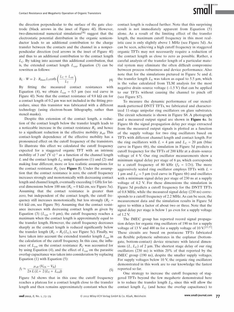
Despite this extension of the contact length, a reduc-tion of the contact length below the transfer length leads to a noticeable increase in the contact resistance RC and hence to a significant reduction in the effective mobility μeff. This contact-length dependence of the effective mobility has a pronounced effect on the cutoff frequency of the transistors. To illustrate this effect we calculated the cutoff frequency expected for a staggered organic TFT with an intrinsic mobility of 3 cm2 (V s)−1 as a function of the channel length L and the contact length LC using Equations (1) and (2) and making four different, more or less realistic assumptions for the contact resistance RC (see Figure 5). Under the assump-tion that the contact resistance is zero, the cutoff frequency increases strongly and monotonically with decreasing contact length and channel length, eventually exceeding 1 GHz for lat-eral dimensions below 100 nm (RC = 0 kΩ cm, see Figure 5a). Assuming that the contact resistance is greater than zero, but independent of the contact length, the cutoff fre-quency still increases monotonically, but less strongly (RC = 0.6 kΩ cm, see Figure 5b). Assuming that the contact resist-ance increases with decreasing contact length as given by Equation (3) (Lext = 0 μm), the cutoff frequency reaches a maximum when the contact length is approximately equal to the transfer length. However, the cutoff frequency decreases sharply as the contact length is reduced significantly below the transfer length (RC = RC(LC), see Figure 5c). Finally, we have taken into account the extended transfer length Lext in the calculation of the cutoff frequency. In this case, the influ-ence of Lext on the contact resistance RC was accounted for by using Equation (4), and the effect of Lext on the parasitic overlap capacitance was taken into consideration by replacing Equation (1) with Equation (5):
fT ≈µeff (VGS− Vth)
2π L(L + 2 (LC + Lext)) (5)
Figure 5d shows that in this case the cutoff frequency reaches a plateau for a contact length close to the transfer length and then remains approximately constant when the
© 2012 Wiley-VCH Verlag Gmsmall 2012, 8, No. 1, 73–79
contact length is reduced further. Note that this surprising result is not immediately apparent from Equation (5) alone. As a result of the limiting effect of the transfer length, the maximum cutoff frequency in this most real-istic case is only slightly above 1 MHz (see Figure 5d). As can be seen, achieving a high cutoff frequency in staggered organic TFTs may not necessarily require a reduction of the contact length as close to zero as possible. Rather, a careful analysis of the transfer length of a particular mate-rial system may eliminate the often difficult compromise between process robustness and device performance. Also note that for the simulations pictured in Figure 5c and d, the transfer length LT was taken as equal to 5.5 μm, which is the value calculated from TLM analysis for the most negative drain–source voltage (–1.5 V) that can be applied to our TFTs without causing the channel to pinch off (see Figure S7).
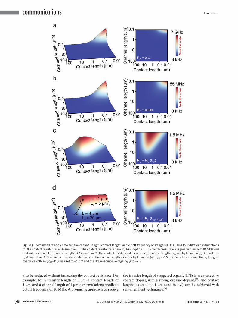
To measure the dynamic performance of our stencil-mask-patterned DNTT TFTs, we fabricated and character-ized 11-stage unipolar ring oscillators on glass substrates. The circuit schematic is shown in Figure S8. A photograph and a measured output signal are shown in Figure 6a. In Figure 6b the signal propagation delay per stage extracted from the measured output signals is plotted as a function of the supply voltage for two ring oscillators based on TFTs with different channel length and contact length. For the ring oscillators with L = 4 μm and LC = 20 μm (blue curve in Figure 6b), the simulation in Figure 5d predicts a cutoff frequency for the TFTs of 200 kHz at a drain–source voltage of 4 V. Our ring oscillator measurements show a minimum signal delay per stage of 6 μs, which corresponds to a cutoff frequency of 80 kHz (fT = 1/2τ). The more aggressively scaled ring oscillator employs TFTs with L = 1 μm and LC = 5 μm (red curve in Figure 6b) and oscillates with a minimum signal delay per stage of 230 ns at a supply voltage of 4.2 V. For these dimensions the simulation in Figure 5d predicts a cutoff frequency for the DNTT TFTs of 0.8 MHz, while the measured signal delay (230 ns) corre-sponds to a cutoff frequency of 2.2 MHz. As can be seen, the measurement data and the simulation results in Figure 5d agree to within a factor of about two or three. Note that the signal delay per stage is below 1 μs even for a supply voltage of 1.2 V.
The IMEC group has reported record signal propaga-tion delays for organic ring oscillators of 190 ns for a supply voltage of 13 V and 400 ns for a supply voltage of 10 V.[15,37] These circuits are based on pentacene TFTs fabricated on flexible polymeric substrates in the coplanar (bottom-gate, bottom-contact) device structure with lateral dimen-sions (L, LC) of 2 μm. The shortest stage delay of our ring oscillators (230 ns) is within 20% of that reported by the IMEC group (190 ns), despite the smaller supply voltages. For supply voltages below 10 V, the organic ring oscillators demonstrated in this work are to our knowledge the fastest reported so far.
One strategy to increase the cutoff frequency of stag-gered TFTs beyond the few megahertz demonstrated here is to reduce the transfer length LT, since this will allow the contact length LC (and hence the overlap capacitance) to
77www.small-journal.combH & Co. KGaA, Weinheim
F. Ante et al.
78
communications
Figure 5. Simulated relation between the channel length, contact length, and cutoff frequency of staggered TFTs using four different assumptions for the contact resistance. a) Assumption 1: The contact resistance is zero. b) Assumption 2: The contact resistance is greater than zero (0.6 kΩ cm) and independent of the contact length. c) Assumption 3: The contact resistance depends on the contact length as given by Equation (3): Lext = 0 μm. d) Assumption 4: The contact resistance depends on the contact length as given by Equation (4): Lext = 0.5 μm. For all four simulations, the gate overdrive voltage (VGS–Vth) was set to –1.6 V and the drain–source voltage (VDS) to –4 V.
also be reduced without increasing the contact resistance. For example, for a transfer length of 1 μm, a contact length of 1 μm, and a channel length of 1 μm our simulations predict a cutoff frequency of 10 MHz. A promising approach to reduce
www.small-journal.com © 2012 Wiley-VCH Ve
the transfer length of staggered organic TFTs is area-selective contact doping with a strong organic dopant,[32] and contact lengths as small as 1 μm (and below) can be achieved with self-alignment techniques.[8]
rlag GmbH & Co. KGaA, Weinheim small 2012, 8, No. 1, 73–79
Contact Resistance and Megahertz Operation of Organic Transistors
Figure 6. Unipolar ring oscillators based on DNTT TFTs. a) Output signal of a ring oscillator based on DNTT TFTs with a channel length of 1 μm and a contact length of 5 μm measured at a supply voltage of 3.5 V. The inset shows a photograph of the ring oscillator. b) Signal propagation delay per stage as a function of the supply voltage for 11-stage ring oscillators based on DNTT TFTs having a channel length of 4 μm and a contact length of 20 μm, and on TFTs having a channel length of 1 μm and a contact length of 5 μm. For the latter, a minimum signal delay of 230 ns per stage was measured at a supply voltage of 4.2 V.
[1] T. Someya, T. Sekitani, S. Iba, Y. Kato, H. Kawaguchi, T. Sakurai, Proc. Natl. Acad. Sci. USA 2004, 101, 9966.
[2] S. Mannsfeld, B. Tee, R. Stoltenberg, C. Chen, S. Barman, B. Muir, A. Sokolov, C. Reese, Z. Bao, Nat. Mater. 2010, 9, 859.
[3] I. Yagi, N. Hirai, Y. Miyamoto, M. Noda, A. Imaoka, N. Yoneya, K. Nomoto, J. Kasahara, A. Yumoto, T. Urabe, J. Soc. Inf. Display 2008, 16, 15.
[4] G. H. Gelinck, H. E. A. Huitema, E. van Veenendaal, E. Cantatore, L. Schrijnemakers, J. B. P. H. van der Putten, T. C. T. Geuns, M. Beenhakkers, J. B. Giesbers, B. H. Huisman, E. J. Meijer, E. M. Benito, F. J. Touwslager, A. W. Marsman, B. J. E. van Rens, D. M. de Leeuw, Nat. Mater. 2004, 3, 106.
[5] H. Kawaguchi, T. Someya, T. Sekitani, T. Sakurai, IEEE J. Solid-State Circuits 2005, 40, 177.
[6] H. Klauk, Chem. Soc. Rev. 2010, 39, 2643. [7] Y. Y. Noh, N. Zhao, M. Caironi, H. Sirringhaus, Nat. Nanotechnol.
2007, 2, 784. [8] U. Palfinger, C. Auner, H. Gold, A. Haase, J. Kraxner, T. Haber,
M. Sezen, W. Grogger, G. Domann, G. Jakopic, J. R. Krenn, B. Stadlober, Adv. Mater. 2010, 22, 5115.
[9] T. Yamamoto, K. Takimiya, J. Am. Chem. Soc. 2007, 129, 2224.[10] T. W. Kelley, L. D. Boardman, T. D. Dunbar, D. V. Muyres,
M. J. Pellerite, T. P. Smith, J. Phys. Chem. B 2003, 107, 5877.[11] S. Lee, B. Koo, J. Shin, E. Lee, H. Park, H. Kim, Appl. Phys. Lett.
2006, 88, 162109.[12] D. Gundlach, L. Zhou, J. Nichols, T. Jackson, P. Necliudov, M. Shur,
J. Appl. Phys. 2006, 100, 024509.[13] A. Benor, D. Knipp, Org. Electron. 2008, 9, 209.[14] V. Wagner, P. Wobkenberg, A. Hoppe, J. Seekamp, Appl. Phys.
Lett. 2006, 89, 243515.[15] K. Myny, S. Steudel, S. Smout, P. Vicca, F. Furthner, B. van der
Putten, A. Tripathi, G. Gelinck, J. Genoe, W. Dehaene, P. Heremans, Org. Electron. 2010, 11, 1176.
[16] M. Kitamura, Y. Arakawa, Jpn. J. Appl. Phys. 2011, 50, 01BC01.
Supporting Information
Supporting Information is available from the Wiley Online Library or from the author.
© 2012 Wiley-VCH Verlag Gmsmall 2012, 8, No. 1, 73–79
[17] C. Shim, F. Maruoka, R. Hattori, IEEE Trans. Electron Devices 2010, 57, 95.
[18] S. Wang, Y. Yan, K. Tsukagoshi, Appl. Phys. Lett. 2010, 97, 063307.
[19] Y. Yan, X. She, H. Zhu, S. Wang, Org. Electron. 2011, 12, 823.[20] S. Luan, G. Neudeck, J. Appl. Phys. 1992, 72, 766.[21] M. Marinkovic, E. Hashem, K. Chan, A. Gordijn, H. Stiebig,
D. Knipp, Appl. Phys. Lett. 2010, 97, 073502.[22] A. D. Franklin, Z. Chen, Nat. Nanotechnol. 2010, 5, 858.[23] J. Smith, Y. Zhao, C. Yang, J. Appenzeller, 68th Annual Device
Research Conference (DRC) Technical Digest 2010, 139. [24] F. Xia, V. Perebeinos, Y. Lin, Y. Wu, P. Avouris, Nat. Nanotechnol.
2011, 6, 179.[25] D. J. Gundlach, T. N. Jackson, D. G. Schlom, S. F. Nelson, Appl.
Phys. Lett. 1999, 74, 3302.[26] F. Letzkus, J. Butschke, B. Hoefflinger, M. Irmscher, C. Reuter,
R. Springer, A. Ehrmann, J. Mathuni, Microelectron. Eng. 2000, 53, 609.
[27] S. Jin, K. Jung, H. Shin, B. Park, J. Lee, Synth. Met. 2006, 156, 196.[28] K. Sidler, N. Cvetkovic, V. Savu, D. Tsamados, A. Ionescu,
J. Brugger, Procedia Chem. 2009, 1, 762.[29] F. Fleischli, K. Sidler, M. Schaer, V. Savu, J. Brugger, L. Zuppiroli,
Org. Electron. 2010, 12, 336.[30] F. Ante, F. Letzkus, J. Butschke, U. Zschieschang, K. Kern,
J. N. Burghartz, H. Klauk, IEEE International Electron Devices Meeting (IEDM) Technical Digest 2010.
[31] U. Zschieschang, F. Ante, D. Kälblein, T. Yamamoto, K. Takimiya, H. Kuwabara, M. Ikeda, T. Sekitani, T. Someya, J. Blochwitz-Nimoth, H. Klauk, Org. Electron. 2011, 12, 1370.
[32] F. Ante, D. Kälblein, U. Zschieschang, T. W. Canzler, A. Werner, K. Takimiya, M. Ikeda, T. Sekitani, T. Someya, H. Klauk, Small 2011, 7, 1186.
[33] J. Zaumseil, K. Baldwin, J. Rogers, J. Appl. Phys. 2003, 93, 6117.[34] D. K. Schroder, Semiconductor Material and Device Characteriza-
tion, 2nd ed., Wiley, New York 1998.[35] T. J. Richards, H. Sirringhaus, J. Appl. Phys. 2007, 102, 094510.[36] S. Scheinert, G. Paasch, J. Appl. Phys. 2009, 105, 014509.[37] P. Heremans, J. Genoe, S. Steudel, K. Myny, S. Smout,
P. Vicca, C. Grillberger, O. R. Hild, F. Furthner, B. van der Putten, A. K. Tripathi, G. H. Gelinck, IEEE International Electron Devices Meeting (IEDM) Technical Digest 2009.
Received: August 16, 2011Published online: November 17, 2011
79www.small-journal.combH & Co. KGaA, Weinheim

Supporting Information
Contact Resistance and Megahertz Operation of Aggressively Scaled Organic Transistors Frederik Ante, Ute Zschieschang, Kazuo Takimiya, Masaaki Ikeda, Tsuyoshi Sekitani, Takao Someya, Hagen Klauk
1. High-resolution silicon stencil masks 2. Transmission line method (TLM) 3. Contact resistance and intrinsic mobility of DNTT TFTs with large contact length 4. Electrical characteristics of DNTT TFTs with small channel length (L = 1 µm, LC = 200 µm) 5. Effective mobilities of DNTT TFTs with channel lengths ranging from 60 µm to 1 µm 6. Transmission line method on DNTT TFTs with various contact lengths 7. Bias-dependence of the transfer length 8. Ring oscillator circuit schematic 9. Additional references
1

1. High-resolution silicon stencil masks
Figure S1: Scanning electron microscopy (SEM) images of high-resolution silicon stencil masks. The SEM images show parts of a high-resolution silicon stencil mask. The apertures in the 20 µm thick silicon membrane were produced by electron-beam lithography and angle-controlled dry etching. The mask features seen in these images were designed to define the source/drain contacts of a staggered (bottom-gate, top-contact) organic TFT with a channel length of 1 µm.
Figure S2: Atomic force microscopy (AFM) image of stencil-mask-patterned metal structures. The AFM image shows gold source /drain contacts with a thickness of 25 nm deposited onto a 30 nm thick aluminum gate electrode, both patterned using silicon stencil masks to define a channel length of 2 µm and a contact length of 2 µm.
2

2. Transmission line method (TLM) For the transmission line method it is assumed that the total resistance (R) of a field-effect transistor is a series connection of the source resistance (Rsource), the channel resistance (Rchannel), and the drain resistance (Rdrain): drainchannelsource RRRR (S1) Since the transmission line method does not distinguish between source and drain resistance, the contact resistance (RC) is defined as the sum of Rsource and Rdrain (which are usually not the same; [ref. S1]): channelC RRR (S2) Both the contact resistance and the channel resistance are inversely proportional to the channel width (W), so that the following normalization is useful: WRWRWR channelC (S3) Unlike the contact resistance, the channel resistance is proportional to the channel length of the transistor (L): LRWR sheetchannel (S4) where Rsheet is the sheet resistance of the semiconductor layer in the channel region. (Note that the normalization to the channel width is already included in the channel sheet resistance Rsheet.) Thus, the following relation between the total resistance, the contact resistance, the semiconductor sheet resistance (which is assumed to be the same for all TFTs), and the channel length is obtained: LRWRWR sheetC (S5) To extract the contact resistance using the transmission line method, we have utilized TFTs with channel lengths ranging from 60 µm to 1 µm. For each TFT, the drain current (ID) was measured at a fixed gate overdrive voltage (VGS – Vth = -1.6 V) and a fixed drain-source voltage (VDS = -0.1 V), and the total resistance (R) was calculated and normalized to the channel width (W):
WI
VWR
D
DS (S6)
The width-normalized total resistance (RW) of each TFT was then plotted over the channel length (L), as shown in Figure 3a. From this plot, the width-normalized contact resistance (RCW) was extracted by extrapolating the width-normalized total resistance to the channel length at which the channel resistance disappears: 0LWRWRC (S7) The contact resistances we have extracted with this method for DNTT TFTs with different contact lengths are: 0.6 kcm (LC = 200 µm), 0.7 kcm (LC = 20 µm), 1.4 kcm (LC = 5 µm), and 2.2 kcm (LC = 2 µm), as shown in Figure S7a.
3

The relationship between the total resistance, the semiconductor sheet resistance, and the channel length can also be written in the following way: )L2(LRWR Tsheet (S8) where LT is the transfer length. From the RW vs. L plot, the transfer length can be extracted by extrapolating the channel length to a total resistance of zero (RW = 0):
2
0WRLLT
(S9)
The transfer length (LT) is the characteristic length over which 63% of the charge carriers exchange between the contacts and the semiconductor occurs [ref. 34]. The transfer length we have extracted with the TLM method at a drain-source voltage VDS = -0.1 V is LT = 10 µm (see Figure 3a). When the difference between the gate overdrive voltage (VGS – Vth) and the drain-source voltage (VDS) is reduced, the transfer length decreases [ref. S2], as seen in Figure S8. If the contact length is much larger than the transfer length (LC > LT), the area available for the charge exchange between the contact and the semiconductor channel will be relatively large, and hence the contact resistance (RCW) will be relatively small. In contrast, if the contact length is smaller than the transfer length (LC < LT), the area available for the exchange of charge carriers between the contact and the channel across the contact/semiconductor interface will be relatively small, and hence the contact resistance will be relatively large. With a number of assumptions and simplifications, the relationship between the contact length, the transfer length, and the contact resistance can be approximately described as follows [ref. 34]:
T
CTsheetC L
LcothLR2WR (S10)
By taking into account the additional contribution to the contact length from the charge transfer in a non-perpendicular direction [ref. 36], i.e., the extended contact length (Lext), Equation (S10) becomes:
T
extCTsheetC L
LLcothLR2WR (S11)
In addition to the contact resistance and the transfer length, the intrinsic mobility of the charge carriers in the semiconductor (µ0) can also be extracted from the RW vs. L plot. According to Equation (S5), the slope of the RW vs. L curve yields the semiconductor sheet resistance (Rsheet), and according to the charge-sheet model [ref. S3], Rsheet is related to the intrinsic carrier mobility (µ0) as follows:
)VV(CR
1thGSi0
sheet
(S12)
with the gate-dielectric capacitance per unit area Ci, the gate-source voltage VGS, and the threshold voltage Vth. The intrinsic carrier mobility we have extracted for the DNTT TFTs is µ0 = 3 cm2/Vs (see Figure 3b). Note that the influence of the contact resistance on the gate-source voltage was ignored in this analysis.
4

3. Contact resistance and intrinsic mobility of DNTT TFTs with large contact length
Figure S3: Contact resistance and intrinsic mobility of DNTT TFTs with large contact length. a) Width-normalized total resistance of DNTT TFTs with a contact length of 200 µm measured at a
drain-source voltage of -0.1 V as a function of the channel length. From the least-square linear fit of the measurement data, a contact resistance of 0.6 kcm, a semiconductor sheet resistance of 270 k/sq, and a transfer length of 10 µm are extracted. The transfer length describes the characteristic distance along the source and drain contacts over which 63% of the charge carriers are transferred into/out of the organic semiconductor.
b) Intrinsic carrier mobility extracted from the gate-bias dependence of the semiconductor sheet resistance.
5

4. Electrical characteristics of DNTT TFTs with small channel length (L = 1 µm, LC = 200 µm)
Figure S4: Transfer and output characteristics of a DNTT TFT with large contact length, but reduced channel length. The transistor has a channel length of 1 µm and a contact length of 200 µm. From the transfer characteristics, effective mobilities of 0.4 cm2/Vs (in the saturation region) and 0.2 cm2/Vs (in the linear region), an on/off current ratio of 107, a subthreshold swing of 100 mV/decade, and a threshold voltage of -1.4 V are extracted.
6

5. Effective mobilities of DNTT TFTs with channel lengths ranging from 60 µm to 1 µm
Figure S5: Effective mobilities of DNTT TFTs with a contact length of 200 µm as a function of the channel length in the saturation region (red curve) and in the linear region (blue curve). As the channel length is reduced from 60 µm to 1 µm, the relative influence of the contact resistance on the total device resistance increases, and as a result the effective mobilities in both the saturation and the linear region decrease.
7

6. Transmission line method on DNTT TFTs with various contact lengths
Figure S6: TLM analysis on DNTT TFTs with various contact lengths. a) Width-normalized total resistance as a function of the channel length for DNTT TFTs with
contact lengths of 200 µm, 20 µm, 5 µm and 2 µm. Extrapolation of the width-normalized resistance to a channel length of zero yields contact resistances of 0.6 kcm (LC = 200 µm), 0.7 kcm (LC = 20 µm), 1.4 kcm (LC = 5 µm), and 2.2 kcm (LC = 2 µm).
b) Width-normalized total resistance as a function of the channel length for DNTT TFTs with a contact length of 200 µm for different gate-source voltages. The slope of each curve indicates the semiconductor sheet resistance Rsheet. For the maximum gate-source voltage (VGS = -3.0 V), a sheet resistance of 270 k/sq is found. From the relation between the semiconductor sheet resistance and the applied gate-source voltage, the intrinsic carrier mobility in the transistor channel can be calculated, yielding µ0 = 3 cm2/Vs (see Figure 2a).
8

7. Bias-dependence of the transfer length
Figure S7: Bias-dependence of the transfer length. When the difference between the gate overdrive voltage (VGS-Vth) and the drain-source voltage (VDS) is reduced, the transfer length (LT) decreases approximately linearly. This bias-dependence of the transfer length is expected from simulations [ref. S2]. The graph shows experimental data calculated from TLM measurements performed with drain-source voltages ranging from -0.1 V to -1.5 V, showing that the transfer length decreases from 9.5 µm (at VDS = -0.1 V) to 5.5 µm (at VDS = -1.5 V). Ideally, these measurements would have been extended to a drain-source voltage of -4 V, which is the drain-source voltage assumed for the simulations that are summarized in Figure 5. However, if the drain-source voltage was reduced below -1.5 V, the carrier channel would become pinched off at the drain (onset of the saturation region) and thus the assumptions underlying the TLM method would no longer be valid. In principle, the transistor could be kept in the linear regime by making the gate-source voltage more negative as well (below -3 V), but this would eventually cause the gate dielectric to break down. For these reasons it was not possible to calculate the transfer length of our TFTs for drain-source voltages more negative than -1.5 V.
9

8. Ring oscillator circuit schematic
Figure S8: Ring oscillator circuit schematic. a) Circuit schematic of an individual unipolar inverter. b) Schematic of the 11-stage ring oscillator with output stage. The bias voltage VBias was set to -1 V. 9. Additional references S1. J. A. Nichols, D. J. Gundlach, T. N. Jackson, Appl. Phys. Lett. 2003, 83, 2366. S2. C. W. Sohn, T. U. Rim, G. B. Choi, Y.H. Jeong, IEEE Trans. Electron Devices 2010, 57, 986. S3. S. Sze, Physics of Semiconductor Devices, 3rd ed., John Wiley & Sons Inc., New York 2007.
10
Related Documents