CONFOCAL NEXIV VMZ-K Series Confocal NEXIV VMZ-K Series CNC Video Measuring System

Welcome message from author
This document is posted to help you gain knowledge. Please leave a comment to let me know what you think about it! Share it to your friends and learn new things together.
Transcript
En
CONFOCAL NEXIV VMZ-K Series
Confocal NEXIV VMZ-K Series
CNC Video Measuring System

2
Light passing through a pinhole on a spinning Nipkow disk is reflected by the workpiece at the focal point, back through the pinhole. This light is detected as a very narrow DOF confocal image by the camera. If there is no workpiece at the focal point, the light does not reflect back through the pinhole. By moving the focal plane in the vertical direction, the Confocal NEXIV VMZ-K series samples multiple confocal images and combines them to compose a confocal image with height information, provided by Nikon’s unique interpolation technology.
Bright Field Image (Bump) 3D Contour Image (Bonding Wire Loop)
■ Principle of Confocal Optics
3D FOV Measurements Generated with Confocal Images The Confocal NEXIV VMZ-K series, a ground-breaking multifunctional video measuring system, was developed on the strength of Nikon’s leading optomechatronics technology.
- Combines confocal optics and brightfield optics, for fast and accurate evaluation of fine three-
dimensional geometries
- Allows both 2D and height measurements in the same field of view
This series can be optimally used for inspecting precise 3D-shaped samples, including micro bumps,
circuit patterns, and bonding wires, as well as samples with countless points, such as probe cards. The
VMZ-K series can also measure both the shallow recesses and gentle ledges on PCBs.
Light passes through a pinhole
Focused Not focused
Camera
Light source
Pinholes on spinning Nipkow disk
ScanObjective lens
Workpiece
Nikon-Original Low Flare Confocal Optics
Confocal images captured by Z scan are reconstructed in real time into 3D contour maps and EDF (Extended Depth of Focus) images.
3D Contour Image (Bump) EDF Image (Bump)
5 6
1 25 63 4
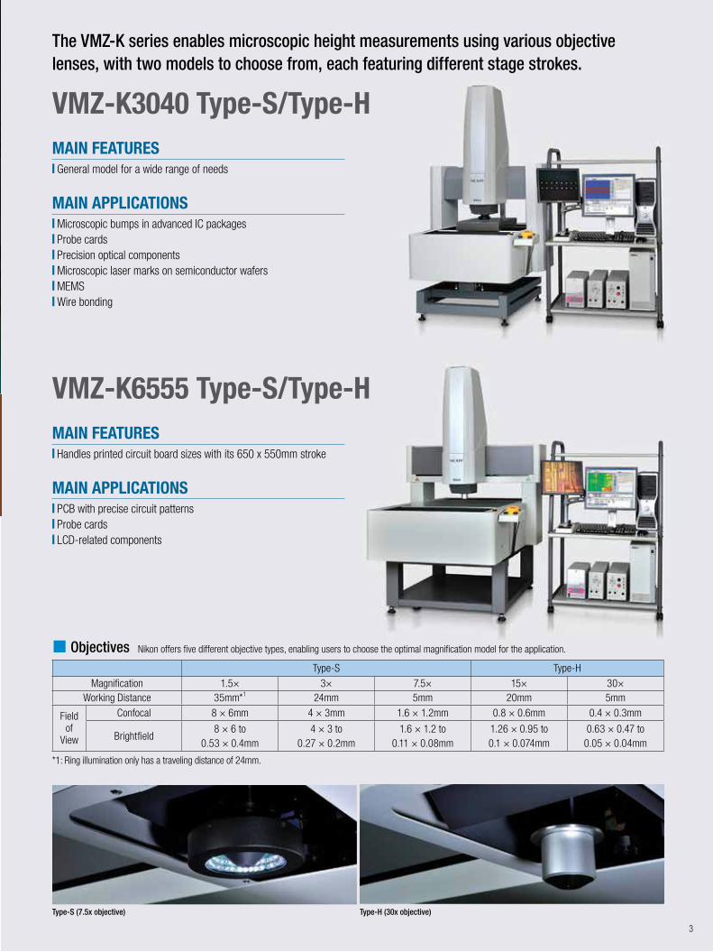
VMZ-K6555 Type-S/Type-H
Type-H (30x objective)
*1: Ring illumination only has a traveling distance of 24mm.
Type-S (7.5x objective)
VMZ-K3040 Type-S/Type-H
The VMZ-K series enables microscopic height measurements using various objective lenses, with two models to choose from, each featuring different stage strokes.
Type-S Type-HMagnification 1.5× 3× 7.5× 15× 30×
Working Distance 35mm*1 24mm 5mm 20mm 5mm
Field of
View
Confocal 8 × 6mm 4 × 3mm 1.6 × 1.2mm 0.8 × 0.6mm 0.4 × 0.3mm
Brightfield8 × 6 to
0.53 × 0.4mm4 × 3 to
0.27 × 0.2mm1.6 × 1.2 to
0.11 × 0.08mm1.26 × 0.95 to0.1 × 0.074mm
0.63 × 0.47 to0.05 × 0.04mm
■ Objectives Nikon offers five different objective types, enabling users to choose the optimal magnification model for the application.
MAIN FEATURES■ Handles printed circuit board sizes with its 650 x 550mm stroke
MAIN APPLICATIONS■ PCB with precise circuit patterns■ Probe cards■ LCD-related components
MAIN FEATURES■ General model for a wide range of needs
MAIN APPLICATIONS■ Microscopic bumps in advanced IC packages■ Probe cards■ Precision optical components ■ Microscopic laser marks on semiconductor wafers ■ MEMS■ Wire bonding
3
2 3 41
2
Light passing through a pinhole on a spinning Nipkow disk is reflected by the workpiece at the focal point, back through the pinhole. This light is detected as a very narrow DOF confocal image by the camera. If there is no workpiece at the focal point, the light does not reflect back through the pinhole. By moving the focal plane in the vertical direction, the Confocal NEXIV VMZ-K series samples multiple confocal images and combines them to compose a confocal image with height information, provided by Nikon’s unique interpolation technology.
Bright Field Image (Bump) 3D Contour Image (Bonding Wire Loop)
■ Principle of Confocal Optics
3D FOV Measurements Generated with Confocal Images The Confocal NEXIV VMZ-K series, a ground-breaking multifunctional video measuring system, was developed on the strength of Nikon’s leading optomechatronics technology.
- Combines confocal optics and brightfield optics, for fast and accurate evaluation of fine three-
dimensional geometries
- Allows both 2D and height measurements in the same field of view
This series can be optimally used for inspecting precise 3D-shaped samples, including micro bumps,
circuit patterns, and bonding wires, as well as samples with countless points, such as probe cards. The
VMZ-K series can also measure both the shallow recesses and gentle ledges on PCBs.
Light passes through a pinhole
Focused Not focused
Camera
Light source
Pinholes on spinning Nipkow disk
ScanObjective lens
Workpiece
Nikon-Original Low Flare Confocal Optics
Confocal images captured by Z scan are reconstructed in real time into 3D contour maps and EDF (Extended Depth of Focus) images.
3D Contour Image (Bump) EDF Image (Bump)
5 6
1 25 63 4
VMZ-K6555 Type-S/Type-H
Type-H (30x objective)
*1: Ring illumination only has a traveling distance of 24mm.
Type-S (7.5x objective)
VMZ-K3040 Type-S/Type-H
The VMZ-K series enables microscopic height measurements using various objective lenses, with two models to choose from, each featuring different stage strokes.
Type-S Type-HMagnification 1.5× 3× 7.5× 15× 30×
Working Distance 35mm*1 24mm 5mm 20mm 5mm
Field of
View
Confocal 8 × 6mm 4 × 3mm 1.6 × 1.2mm 0.8 × 0.6mm 0.4 × 0.3mm
Brightfield8 × 6 to
0.53 × 0.4mm4 × 3 to
0.27 × 0.2mm1.6 × 1.2 to
0.11 × 0.08mm1.26 × 0.95 to0.1 × 0.074mm
0.63 × 0.47 to0.05 × 0.04mm
■ Objectives Nikon offers five different objective types, enabling users to choose the optimal magnification model for the application.
MAIN FEATURES■ Handles printed circuit board sizes with its 650 x 550mm stroke
MAIN APPLICATIONS■ PCB with precise circuit patterns■ Probe cards■ LCD-related components
MAIN FEATURES■ General model for a wide range of needs
MAIN APPLICATIONS■ Microscopic bumps in advanced IC packages■ Probe cards■ Precision optical components ■ Microscopic laser marks on semiconductor wafers ■ MEMS■ Wire bonding
3
2 3 41
4 5
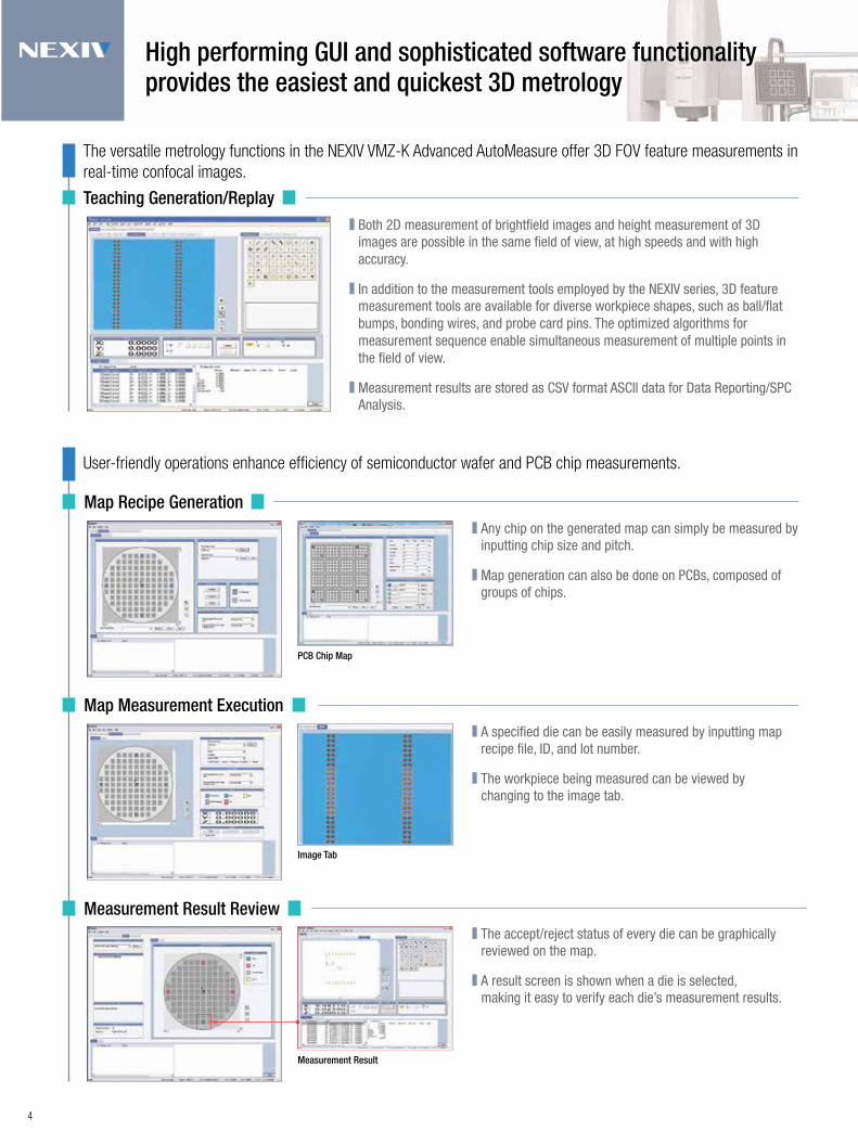
User-friendly operations enhance efficiency of semiconductor wafer and PCB chip measurements.
Measurement Result
High performing GUI and sophisticated software functionality provides the easiest and quickest 3D metrology
The versatile metrology functions in the NEXIV VMZ-K Advanced AutoMeasure offer 3D FOV feature measurements in real-time confocal images.
Teaching Generation/Replay ■ Both 2D measurement of brightfield images and height measurement of 3D
images are possible in the same field of view, at high speeds and with high accuracy.
■ In addition to the measurement tools employed by the NEXIV series, 3D feature measurement tools are available for diverse workpiece shapes, such as ball/flat bumps, bonding wires, and probe card pins. The optimized algorithms for measurement sequence enable simultaneous measurement of multiple points in the field of view.
■ Measurement results are stored as CSV format ASCII data for Data Reporting/SPC Analysis.
■ Any chip on the generated map can simply be measured by inputting chip size and pitch.
■ Map generation can also be done on PCBs, composed of groups of chips.
■ A specified die can be easily measured by inputting map recipe file, ID, and lot number.
■ The workpiece being measured can be viewed by changing to the image tab.
■ The accept/reject status of every die can be graphically reviewed on the map.
■ A result screen is shown when a die is selected, making it easy to verify each die’s measurement results.
Map Recipe Generation
PCB Chip Map
Map Measurement Execution
Image Tab
Measurement Result Review
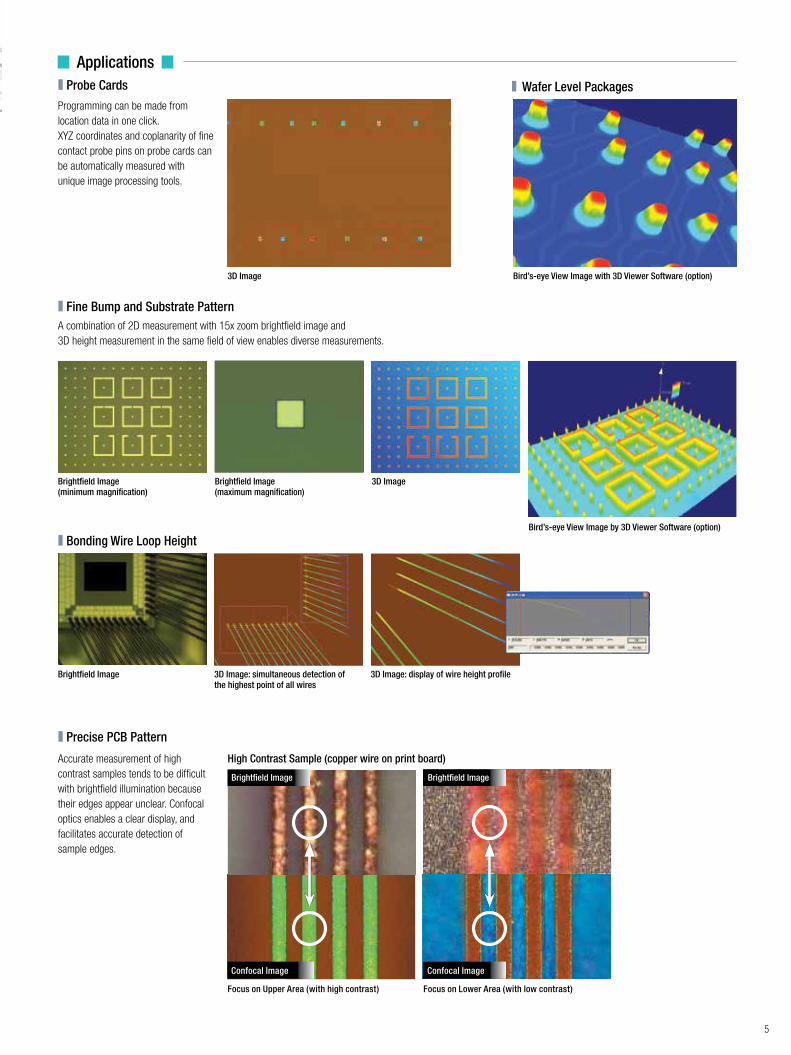
Applications ■ Probe Cards
Programming can be made from location data in one click. XYZ coordinates and coplanarity of fine contact probe pins on probe cards can be automatically measured with unique image processing tools.
Accurate measurement of high contrast samples tends to be difficult with brightfield illumination because their edges appear unclear. Confocal optics enables a clear display, and facilitates accurate detection of sample edges.
Brightfield Image (minimum magnification)
Brightfield Image (maximum magnification)
3D Image
Brightfield Image 3D Image: simultaneous detection of the highest point of all wires
High Contrast Sample (copper wire on print board)
3D Image: display of wire height profile
Bird’s-eye View Image by 3D Viewer Software (option)
■ Fine Bump and Substrate PatternA combination of 2D measurement with 15x zoom brightfield image and 3D height measurement in the same field of view enables diverse measurements.
3D Image Bird’s-eye View Image with 3D Viewer Software (option)
■ Bonding Wire Loop Height
■ Precise PCB Pattern
■ Wafer Level Packages
Brightfield Image
Confocal Image
Focus on Upper Area (with high contrast) Focus on Lower Area (with low contrast)
Brightfield Image
Confocal Image
4 5
User-friendly operations enhance efficiency of semiconductor wafer and PCB chip measurements.
Measurement Result
High performing GUI and sophisticated software functionality provides the easiest and quickest 3D metrology
The versatile metrology functions in the NEXIV VMZ-K Advanced AutoMeasure offer 3D FOV feature measurements in real-time confocal images.
Teaching Generation/Replay ■ Both 2D measurement of brightfield images and height measurement of 3D
images are possible in the same field of view, at high speeds and with high accuracy.
■ In addition to the measurement tools employed by the NEXIV series, 3D feature measurement tools are available for diverse workpiece shapes, such as ball/flat bumps, bonding wires, and probe card pins. The optimized algorithms for measurement sequence enable simultaneous measurement of multiple points in the field of view.
■ Measurement results are stored as CSV format ASCII data for Data Reporting/SPC Analysis.
■ Any chip on the generated map can simply be measured by inputting chip size and pitch.
■ Map generation can also be done on PCBs, composed of groups of chips.
■ A specified die can be easily measured by inputting map recipe file, ID, and lot number.
■ The workpiece being measured can be viewed by changing to the image tab.
■ The accept/reject status of every die can be graphically reviewed on the map.
■ A result screen is shown when a die is selected, making it easy to verify each die’s measurement results.
Map Recipe Generation
PCB Chip Map
Map Measurement Execution
Image Tab
Measurement Result Review
Applications ■ Probe Cards
Programming can be made from location data in one click. XYZ coordinates and coplanarity of fine contact probe pins on probe cards can be automatically measured with unique image processing tools.
Accurate measurement of high contrast samples tends to be difficult with brightfield illumination because their edges appear unclear. Confocal optics enables a clear display, and facilitates accurate detection of sample edges.
Brightfield Image (minimum magnification)
Brightfield Image (maximum magnification)
3D Image
Brightfield Image 3D Image: simultaneous detection of the highest point of all wires
High Contrast Sample (copper wire on print board)
3D Image: display of wire height profile
Bird’s-eye View Image by 3D Viewer Software (option)
■ Fine Bump and Substrate PatternA combination of 2D measurement with 15x zoom brightfield image and 3D height measurement in the same field of view enables diverse measurements.
3D Image Bird’s-eye View Image with 3D Viewer Software (option)
■ Bonding Wire Loop Height
■ Precise PCB Pattern
■ Wafer Level Packages
Brightfield Image
Confocal Image
Focus on Upper Area (with high contrast) Focus on Lower Area (with low contrast)
Brightfield Image
Confocal Image

6
Optional Software Optional Hardware
■ Image Archiving and Processing Software - EDF/Stitching Express
The EDF/Stitching Express software creates an image archiving library for confocal and brightfield images, and provides post-image processing functionalities, such as EDF and large-area image stitching.
■ Wide FOV Optics (for high-magnification optical heads)
Wide field of view optics aids in the selection of the area to be measured and the creation of programs with high-magnification optical heads.
Compatible optical head: 15x, 30x Field of view: 4.8mm x 3.6mmWorking distance: 40.6mmMain optical head offset: 64mmIllumination: Episcopic illumination only
Wide FOV optics effective ranges (mm)VMZ-K3040 236(X) x 400(Y)VMZ-K6555 586(X) x 550(Y)
■ 3D Surface Metrology Analysis Software - MountainsMap X
The MountainsMap X is a powerful software for surface metrology analysis. It provides the rich functionality of 3D visualization, cross-sectional view, 2D and 3D roughness, and other parameters based on the latest ISO standards.
FOV Comparison
Stitching
■ Wafer Holder (vacuum chuck)
Firmly secures wafers to be measured with a vacuum chuck system and is compatible with 125mm, 150mm, 200mm and 300mm wafer sizes.
Wide FOV optics
Main optics
Wide FOV Optics
Contour Image
Step Sample (contour)
Profile
Bird’s-eye View Image Partial Image Roughness Data
Bird’s-eye View Image
30x Objective 1x (0.4mm x 0.3mm)
■ Dimensional Diagram
880950
1150
456
850
1970
165
490
16001050 300
1150850
880
1350
115019
70
125077
1850
Unit: mm Unit: mm
7
VMZ-K6555VMZ-K3040

6
Optional Software Optional Hardware
■ Image Archiving and Processing Software - EDF/Stitching Express
The EDF/Stitching Express software creates an image archiving library for confocal and brightfield images, and provides post-image processing functionalities, such as EDF and large-area image stitching.
■ Wide FOV Optics (for high-magnification optical heads)
Wide field of view optics aids in the selection of the area to be measured and the creation of programs with high-magnification optical heads.
Compatible optical head: 15x, 30x Field of view: 4.8mm x 3.6mmWorking distance: 40.6mmMain optical head offset: 64mmIllumination: Episcopic illumination only
Wide FOV optics effective ranges (mm)VMZ-K3040 236(X) x 400(Y)VMZ-K6555 586(X) x 550(Y)
■ 3D Surface Metrology Analysis Software - MountainsMap X
The MountainsMap X is a powerful software for surface metrology analysis. It provides the rich functionality of 3D visualization, cross-sectional view, 2D and 3D roughness, and other parameters based on the latest ISO standards.
FOV Comparison
Stitching
■ Wafer Holder (vacuum chuck)
Firmly secures wafers to be measured with a vacuum chuck system and is compatible with 125mm, 150mm, 200mm and 300mm wafer sizes.
Wide FOV optics
Main optics
Wide FOV Optics
Contour Image
Step Sample (contour)
Profile
Bird’s-eye View Image Partial Image Roughness Data
Bird’s-eye View Image
30x Objective 1x (0.4mm x 0.3mm)
■ Dimensional Diagram
880950
1150
456
850
1970
165
490
16001050 300
1150850
880
1350
1150
1970
1250
771850
Unit: mm Unit: mm
7
VMZ-K6555VMZ-K3040
EnThis brochure is printed on recycled paper made from 40% used material.Printed in Japan (1603-02)T Code No.2CE-IDXH-1
Specifications and equipment are subject to change without any notice or obligation on the part of the manufacturer. March 2016©2016 NIKON CORPORATION
* Monitor images are simulated. Company names and product names appearing in this brochure are their registered trademarks or trademarks.
NIKON METROLOGY, INC.12701 Grand River Avenue, Brighton, MI 48116 U.S.A.phone: +1-810-220-4360 fax: +1-810-220-4300E-mail: [email protected]://us.nikonmetrology.com/http://www.nikoninstruments.com/
NIKON METROLOGY EUROPE NVGeldenaaksebaan 329, 3001 Leuven, Belgiumphone: +32-16-74-01-00 fax: +32-16-74-01-03E-mail: [email protected]://www.nikonmetrology.com/
NIKON INSTRUMENTS (SHANGHAI) CO., LTD.CHINA phone: +86-21-6841-2050 fax: +86-21-6841-2060(Beijing branch) phone: +86-10-5831-2028 fax: +86-10-5831-2026(Guangzhou branch) phone: +86-20-3882-0552 fax: +86-20-3882-0580
NIKON SINGAPORE PTE LTDSINGAPORE phone: +65-6559-3651 fax: +65-6559-3668
NIKON MALAYSIA SDN BHDMALAYSIA phone: +60-3-7809-3688 fax: +60-3-7809-3633
P.T. NIKON INDONESIAINDONESIA phone: +62-267 8643949 fax: +62-267 8643950
NIKON SALES (THAILAND) CO., LTD.THAILAND phone: +66-2633-5100 fax: 66-2633-5191
NIKON INSTRUMENTS KOREA CO., LTD.KOREA phone: +82-2-2186-8400 fax: +82-2-555-4415
NIKON INDIA PRIVATE LIMITEDINDIA phone: +91-124-4688500 fax: +91-124-4688527
NIKON INSTRUMENTS S.p.A.ITALY phone: +39-055-300-96-01 fax: +39-055-30-09-93
NIKON METROLOGY UK LTD.UNITED KINGDOM phone: +44-1332-811-349 fax: +44-1332-639-881E-mail: [email protected]
NIKON METROLOGY SARLFRANCE phone: +33-1-60-86-09-76 fax: +33-1-60-86-57-35E-mail: [email protected]
NIKON METROLOGY GMBHGERMANY phone: +49-6023-91733-0 fax: +49-6023-91733-229E-mail: [email protected]
NIKON CORPORATIONShinagawa Intercity Tower C, 2-15-3, Konan, Minato-ku, Tokyo 108-6290, Japanphone: +81-3-6433-3701 fax: +81-3-6433-3784 http://www.nikon.com/products/industrial-metrology/
WARNINGTO ENSURE CORRECT USAGE, READ THE CORRESPONDING MANUALS CAREFULLY BEFORE USING YOUR EQUIPMENT.
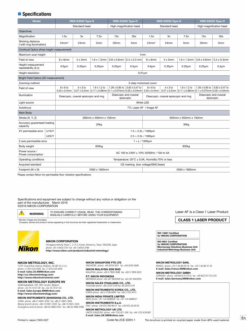
■ SpecificationsModel VMZ-K3040 Type-S VMZ-K3040 Type-H VMZ-K6555 Type-S VMZ-K6555 Type-H
Standard head High-magnification head Standard head High-magnification head
Objectives
Magnification 1.5x 3x 7.5x 15x 30x 1.5x 3x 7.5x 15x 30x
Working distance (*with ring illumination) 24mm* 24mm 5mm 20mm 5mm 24mm* 24mm 5mm 20mm 5mm
Confocal Optics (Area height measurement)
Maximum scan height 1mm
Field of view 8 x 6mm 4 x 3mm 1.6 x 1.2mm 0.8 x 0.6mm 0.4 x 0.3 mm 8 x 6mm 4 x 3mm 1.6 x 1.2mm 0.8 x 0.6mm 0.4 x 0.3mm
Height measurement repeatability (2σ) 0.6μm 0.35μm 0.25μm 0.25μm 0.2μm 0.6μm 0.35μm 0.25μm 0.25μm 0.2μm
Height resolution 0.01μm
Bright Field Optics (2D measurement)
Zooming method 5-step motorized zoom
Field of view 8 x 6 to0.53 x 0.4mm
4 x 3 to0.27 x 0.2mm
1.6 x 1.2 to0.11 x 0.08mm
1.26 x 0.95 to0.1 x 0.074mm
0.63 x 0.47 to0.05 x 0.04mm
8 x 6 to0.53 x 0.4mm
4 x 3 to0.27 x 0.2mm
1.6 x 1.2 to0.11 x 0.08mm
1.26 x 0.95 to0.1 x 0.074mm
0.63 x 0.47 to0.05 x 0.04mm
Illumination Diascopic, coaxial episcopic and ring Diascopic and coaxial episcopic Diascopic, coaxial episcopic and ring Diascopic and coaxial
episcopic
Light source White LED
Autofocus TTL Laser AF / Image AF
Main Body
Stroke (X, Y, Z) 300mm x 400mm x 150mm 650mm x 550mm x 150mm
Accuracy guaranteed loading capacity 20kg 30kg
XY permissible error
U1X/Y 1.5 + 2.5L / 1000μm
U2X/Y 2.5 + 2.5L / 1000μm
Z axis permissible error 1 + L / 1000μm
Body weight 830kg 830kg
Power source / Power consumption AC 100 to 240V ± 10% 50/60Hz / 10A to 5A
Operating conditions Temperature: 20°C ± 0.5K, Humidity:70% or less
Acquired standard CE marking (low voltage/EMC/laser)
Footprint (W x D) 2500 x 1600mm 2500 x 1900mm
Please contact Nikon for permissible floor vibration specifications.
Laser AF is a Class 1 Laser Product
CLASS 1 LASER PRODUCT
ISO 14001 Certifiedfor NIKON CORPORATION
ISO 9001 Certifiedfor NIKON CORPORATIONMicroscope Solutions Business UnitIndustrial Metrology Business Unit
Related Documents