14982 Phys. Chem. Chem. Phys., 2012, 14, 14982–14998 This journal is c the Owner Societies 2012 Cite this: Phys. Chem. Chem. Phys., 2012, 14, 14982–14998 Applications of light scattering in dye-sensitized solar cells Qifeng Zhang, a Daniel Myers, a Jolin Lan, a Samson A. Jenekhe bc and Guozhong Cao* ab Received 4th September 2012, Accepted 4th September 2012 DOI: 10.1039/c2cp43089d Light scattering is a method that has been employed in dye-sensitized solar cells for optical absorption enhancement. In conventional dye-sensitized solar cells, large TiO 2 particles with sizes comparable to the wavelength of visible light are used as scatterers by either being mixed into the nanocrystalline film to generate light scattering or forming a scattering layer on the top of the nanocrystalline film to reflect the incident light, with the aim to extend the traveling distance of incident light within the photoelectrode film. Recently, hierarchical nanostructures, for example nanocrystallite aggregates (among others), have been applied to dye-sensitized solar cells. When used to form a photoelectrode film, these hierarchical nanostructures have demonstrated a dual function: providing large specific surface area; and generating light scattering. Some other merits, such as the capability to enhance electron transport, have been also observed on the hierarchically structured photoelectrode films. Hierarchical nanostructures possessing an architecture that may provide sufficient internal surface area for dye adsorption and meanwhile may generate highly effective light scattering, make them able to create photoelectrode films with optical absorption significantly more efficient than the dispersed nanoparticles used in conventional dye-sensitized solar cells. This allows reduction of the thickness of the photoelectrode film and thus lowering of the charge recombination in dye-sensitized solar cells, making it possible to increase further the efficiency of existing dye-sensitized solar cells. 1. Introduction Solar cells are a type of device based on the photovoltaic effect to convert solar energy to electricity. 1 So far, the development of solar cells has undergone three generations. First generation solar cells are built on V or II–VI group single crystal a Department of Materials Science and Engineering, University of Washington, Seattle, WA 98195, USA b Department of Chemical Engineering, University of Washington, Seattle, WA 98195, USA c Department of Chemistry, University of Washington, Seattle, WA 98195, USA. E-mail: [email protected] Qifeng Zhang Qifeng Zhang earned his PhD degree from Peking Univer- sity. Currently he is Research Assistant Professor in the Department of Materials Science and Engineering at University of Washington. His research interests involve engineering nano-structured materials for applications to electrical devices, including solar cells, UV light-emitting diodes (LEDs), field-effect transistors (FETs), and gas sensors. His current research is focused on dye-sensitized solar cells (DSCs), Cu 2 ZnSnS 4 (CZTS)-based thin film solar cells, quantum dot solar cells, and organic/inorganic hybrid solar cells. Samson A. Jenekhe Samson A. Jenekhe received his BS degree from Michigan Technological University in 1977 and PhD degree from University of Minnesota in 1985. He is currently Boeing- Martin Professor of Chemical Engineering and Professor of Chemistry in the Department of Chemical Engineering at University of Washington. His research interests involve: (1) organic electronics and optoelectronics, including thin film transistors, solar cells, and LEDs; (2) self-assembly and nanotechnology, including block copolymers, nanowires, and multicomponent self-assembly; and (3) polymer science, including synthesis, processing, properties, and photonic applications. PCCP Dynamic Article Links www.rsc.org/pccp PERSPECTIVE Downloaded by University of Washington on 29 October 2012 Published on 05 September 2012 on http://pubs.rsc.org | doi:10.1039/C2CP43089D View Online / Journal Homepage / Table of Contents for this issue

Welcome message from author
This document is posted to help you gain knowledge. Please leave a comment to let me know what you think about it! Share it to your friends and learn new things together.
Transcript
14982 Phys. Chem. Chem. Phys., 2012, 14, 14982–14998 This journal is c the Owner Societies 2012
Cite this: Phys. Chem. Chem. Phys., 2012, 14, 14982–14998
Applications of light scattering in dye-sensitized solar cells
Qifeng Zhang,aDaniel Myers,
aJolin Lan,
aSamson A. Jenekhe
bcand
Guozhong Cao*ab
Received 4th September 2012, Accepted 4th September 2012
DOI: 10.1039/c2cp43089d
Light scattering is a method that has been employed in dye-sensitized solar cells for optical
absorption enhancement. In conventional dye-sensitized solar cells, large TiO2 particles with sizes
comparable to the wavelength of visible light are used as scatterers by either being mixed into the
nanocrystalline film to generate light scattering or forming a scattering layer on the top of the
nanocrystalline film to reflect the incident light, with the aim to extend the traveling distance of
incident light within the photoelectrode film. Recently, hierarchical nanostructures, for example
nanocrystallite aggregates (among others), have been applied to dye-sensitized solar cells. When
used to form a photoelectrode film, these hierarchical nanostructures have demonstrated a dual
function: providing large specific surface area; and generating light scattering. Some other merits,
such as the capability to enhance electron transport, have been also observed on the hierarchically
structured photoelectrode films. Hierarchical nanostructures possessing an architecture that may
provide sufficient internal surface area for dye adsorption and meanwhile may generate highly
effective light scattering, make them able to create photoelectrode films with optical absorption
significantly more efficient than the dispersed nanoparticles used in conventional dye-sensitized
solar cells. This allows reduction of the thickness of the photoelectrode film and thus lowering of
the charge recombination in dye-sensitized solar cells, making it possible to increase further the
efficiency of existing dye-sensitized solar cells.
1. Introduction
Solar cells are a type of device based on the photovoltaic effect
to convert solar energy to electricity.1 So far, the development
of solar cells has undergone three generations. First generation
solar cells are built on V or II–VI group single crystal
aDepartment of Materials Science and Engineering,University of Washington, Seattle, WA 98195, USA
bDepartment of Chemical Engineering, University of Washington,Seattle, WA 98195, USA
cDepartment of Chemistry, University of Washington, Seattle,WA 98195, USA. E-mail: [email protected]
Qifeng Zhang
Qifeng Zhang earned his PhDdegree from Peking Univer-sity. Currently he is ResearchAssistant Professor in theDepartment of MaterialsScience and Engineering atUniversity of Washington.His research interests involveengineering nano-structuredmaterials for applications toelectrical devices, includingsolar cells, UV light-emittingdiodes (LEDs), field-effecttransistors (FETs), and gassensors. His current researchis focused on dye-sensitized
solar cells (DSCs), Cu2ZnSnS4 (CZTS)-based thin film solarcells, quantum dot solar cells, and organic/inorganic hybridsolar cells.
Samson A. Jenekhe
Samson A. Jenekhe receivedhis BS degree from MichiganTechnological University in1977 and PhD degree fromUniversity of Minnesota in1985. He is currently Boeing-Martin Professor of ChemicalEngineering and Professor ofChemistry in the Departmentof Chemical Engineering atUniversity of Washington.His research interests involve:(1) organic electronics andoptoelectronics, including thinfilm transistors, solar cells,and LEDs; (2) self-assembly
and nanotechnology, including block copolymers, nanowires, andmulticomponent self-assembly; and (3) polymer science, includingsynthesis, processing, properties, and photonic applications.
PCCP Dynamic Article Links
www.rsc.org/pccp PERSPECTIVE
Dow
nloa
ded
by U
nive
rsity
of
Was
hing
ton
on 2
9 O
ctob
er 2
012
Publ
ishe
d on
05
Sept
embe
r 20
12 o
n ht
tp://
pubs
.rsc
.org
| do
i:10.
1039
/C2C
P430
89D
View Online / Journal Homepage / Table of Contents for this issue
This journal is c the Owner Societies 2012 Phys. Chem. Chem. Phys., 2012, 14, 14982–14998 14983
semiconductors, with which a bulk p–n junction is established
to separate photogenerated electron–hole pairs. The theoretical
limit to the efficiency of single junction solar cells based on these
materials is about 31%.2 Currently, the first generation solar
cells are most represented in commercial production, with
about 90% of the current market share. The second generation
is also derived mainly from the V or II–VI group semiconductor
materials, however, with the consideration of lowering costs.
Owing to the development of vacuum deposition technology,
the devices have been developed using thin films so as to reduce
the material mass and thus lowering the costs. The second
generation solar cells feature conversion efficiencies typically
in a range of 18–20%. Although such conversion efficiencies
have been able to meet the requirements for most uses in low
power electrical appliances, the costs of the materials and of
manufacturing are still somewhat too high and therefore limit
practical application of these cells.
The high cost of the first and second generation solar cells
has motivated the development of third generation solar cells
based on new materials, structures and concepts. The third
generation solar cells are represented by polymer-based organic
solar cells and Gratzel-type dye-sensitized solar cells (DSCs).
These solar cells feature relatively low production costs while
providing decent conversion efficiencies that may be satisfactory
for practical applications. Comparing these two kinds of solar
cells, the polymer-based organic solar cells are thought to have
great potential due to the diversity of polymers available
through molecular design, which potentially allows the creation
of a highly efficient p–n junction and thus deliver very high
efficiency solar cells. Recently, the record efficiencies of B6%
for single-layer polymer solar cells and 8.62% for tandem
polymer solar cells have been announced.3 However, the lack
of chemical stability of the polymer materials is still a problem
for the polymer solar cells, which must be exposed to long term
sunlight under ambient conditions. Being so far superior to
polymer solar cells, DSCs have been able to provide conversion
efficiencies as high as 11–12%,4,5 and the lifetime of DSCs has
been demonstrated as even longer than 20 years in operating
condition, with only a slight degradation of the dye materials.4
In addition, the very low cost in materials and ease of
manufacturing are also the reasons that make the DSCs still
attractive nowadays.
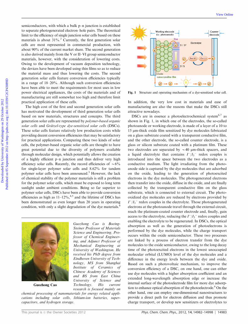
DSCs are in essence a photoelectrochemical system6,7 as
shown in Fig. 1, in which one of the electrodes, the so-called
photoanode or working electrode, is made of a layer of a 10 to
15 mm-thick oxide film sensitized by dye molecules fabricated
on a glass substrate coated with a transparent conductive film,
and the other electrode, the so-called counter electrode, is a
glass or silicon substrate coated with a platinum film. These
two electrodes are separated by B40 mm-thick spacers, and
a liquid electrolyte that contains I�/I3� redox couples is
introduced into the space between the two electrodes as a
conductive medium. The light irradiating from the photo-
anode side is captured by the dye molecules that are adsorbed
on the oxide, leading to the generation of photoexcited
electrons in the dye molecules. The photogenerated electrons
then transfer into the oxide, diffuse in the oxide, and are finally
collected by the transparent conductive film on the glass
substrate, which is connected to external circuit. The photo-
oxidized dye molecules are reduced by electrons provided by
I�/I3� redox couples in the electrolyte. Those photogenerated
electrons at the photoanode travel through the external circuit,
reach the platinum-coated counter electrode and, finally, gain
access to the electrolyte, reducing the I�/I3� redox couples and
enabling the electrolyte to be regenerated. In DSCs, the optical
absorption as well as the generation of photoelectrons is
performed by the dye molecules, while the charge transport
occurs within the oxide semiconductor. These two processes
are linked by a process of electron transfer from the dye
molecules to the oxide semiconductor, owing to the long decay
time of the photoexcited electrons in the lowest unoccupied
molecular orbital (LUMO) level of the dye molecules and a
difference in the energy levels between the dye and oxide.
Based on such a photovoltaic mechanism, to improve the
conversion efficiency of a DSC, on one hand, one can either
use dye molecules with a higher absorption coefficient and an
extended long-wavelength absorption edge or increase the
internal surface of the photoelectrode film for more dye adsorp-
tion to enhance optical absorption of the photoelectrode.8 On the
other hand, one can employ one-dimensional nanostructures to
provide a direct path for electron diffusion and thus promote
charge transport, or develop new sensitizers or electrolytes to
Fig. 1 Structure and operating mechanism of a dye-sensitized solar cell.
Guozhong Cao
Guozhong Cao is Boeing-Steiner Professor of MaterialsScience and Engineering, Pro-fessor of Chemical Engineer-ing, and Adjunct Professor ofMechanical Engineering atUniversity of Washington. Hereceived his PhD degree fromEindhoven University of Tech-nology, MS from ShanghaiInstitute of Ceramics ofChinese Academy of Sciencesand BS from East ChinaUniversity of Science andTechnology. His currentresearch is focused mainly on
chemical processing of nanomaterials for energy related appli-cations including solar cells, lithium-ion batteries, super-capacitors, and hydrogen storage.
Dow
nloa
ded
by U
nive
rsity
of
Was
hing
ton
on 2
9 O
ctob
er 2
012
Publ
ishe
d on
05
Sept
embe
r 20
12 o
n ht
tp://
pubs
.rsc
.org
| do
i:10.
1039
/C2C
P430
89D
View Online
14984 Phys. Chem. Chem. Phys., 2012, 14, 14982–14998 This journal is c the Owner Societies 2012
reduce the recombination in DSCs.9–11 In addition to the
aforementioned ways of improving DSC performance, light
scattering is another important method that has been adopted
to enhance the conversion efficiency of DSCs.12 The basic
idea of a light scattering method is to confine the light
propagation and extend the traveling distance of light
within the photoelectrode film so as to increase the opportu-
nity of the photons to be absorbed by the dye molecules, and
in this way, to enhance the light harvesting efficiency of the
photoelectrode as well as the conversion efficiency of the
solar cells.
This paper reviews the applications of light scattering in
DSCs over the past two decades and some recent progress in
this topic. It will show that, conventionally, the light scattering
can be generated by introducing submicron-sized large particles
into nanocrystalline films, which serve as the basic absorbing
layer in traditional DSCs. The large particles as light scatterers
may either be embedded into the nanocrystalline film to form a
mixed structure photoelectrode film, or be applied onto the
nanocrystalline film to form a light scattering layer and result
in a double-layer structure photoelectrode film. Besides the use
of large particles combined with nanocrystalline films, recently
a class of hierarchical nanostructure consisting of nano-sized
oxide crystallites assembled into spherical aggregates has been
developed for application in DSCs, with particular emphasis
on providing a large surface area and generating light scatter-
ing simultaneously so as to overcome the drawback of con-
ventional methods using large particles for light scattering, in
which the large particles unavoidably lead to a loss of internal
surface area of the photoelectrode film in the case of mixed
structures, or the incident light is only reflected once with the
double-layer structure.13,14 Through using a photoelectrode
film constructed with hierarchical nanostructure called nano-
crystallite aggregates, the Cao group has gained a more than
140% increase in the conversion efficiency of ZnO-based
DSCs.15,16 In the outlook section, hierarchical nanostructures
are emphasized as promising materials for achieving high
efficiency DSCs in view of their dual function in providing a
large surface area and generating effective light scattering,
which allows a reduction in the thickness of the photoelectrode
film and therefore a decrease in the rate of charge recombina-
tion. While the focus of this paper is on a review of technical
issues regarding the utilization of light scattering effects in
DSCs to enhance the optical absorption, it is expected that this
paper may also convey insight about how the materials can be
tailored to benefit solar cells in terms of light harvesting and
electron transport.
2. Light scattering theory
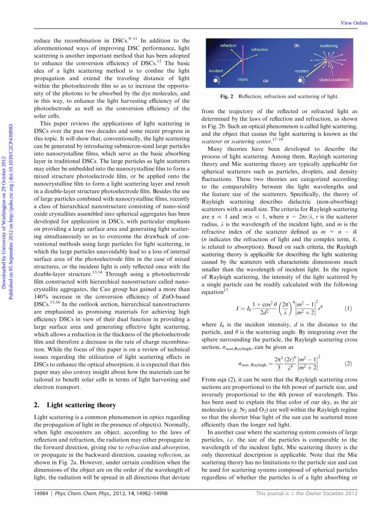
Light scattering is a common phenomenon in optics regarding
the propagation of light in the presence of object(s). Normally,
when light encounters an object, according to the laws of
reflection and refraction, the radiation may either propagate in
the forward direction, giving rise to refraction and absorption,
or propagate in the backward direction, causing reflection, as
shown in Fig. 2a. However, under certain condition when the
dimensions of the object are on the order of the wavelength of
light, the radiation will be spread in all directions that deviate
from the trajectory of the reflected or refracted light as
determined by the laws of reflection and refraction, as shown
in Fig. 2b. Such an optical phenomenon is called light scattering,
and the object that causes the light scattering is known as the
scatterer or scattering center.17–19
Many theories have been developed to describe the
process of light scattering. Among them, Rayleigh scattering
theory and Mie scattering theory are typically applicable for
spherical scatterers such as particles, droplets, and density
fluctuations. These two theories are categorized according
to the comparability between the light wavelengths and
the feature size of the scatterers. Specifically, the theory of
Rayleigh scattering describes dielectric (non-absorbing)
scatterers with a small size. The criteria for Rayleigh scattering
are a { 1 and |m|a { 1, where a = 2pr/l, r is the scatterer
radius, l is the wavelength of the incident light, and m is the
refractive index of the scatterer defined as m = n � ik
(n indicates the refraction of light and the complex term, k,
is related to absorption). Based on such criteria, the Rayleigh
scattering theory is applicable for describing the light scattering
caused by the scatterers with characteristic dimensions much
smaller than the wavelength of incident light. In the region
of Rayleigh scattering, the intensity of the light scattered by
a single particle can be readily calculated with the following
equation17
I ¼ I01þ cos2 y
2d2
2pl
� �4m2 � 1
m2 þ 2
��������2
r6 ð1Þ
where I0 is the incident intensity, d is the distance to the
particle, and y is the scattering angle. By integrating over the
sphere surrounding the particle, the Rayleigh scattering cross
section, sscat,Rayleigh, can be given as
sscat; Rayleigh ¼2p5
3
ð2rÞ6
l4m2 � 1
m2 þ 2
��������2
ð2Þ
From eqn (2), it can be seen that the Rayleigh scattering cross
sections are proportional to the 6th power of particle size, and
inversely proportional to the 4th power of wavelength. This
has been used to explain the blue color of our sky, as the air
molecules (e.g. N2 and O2) are well within the Rayleigh regime
so that the shorter blue light of the sun can be scattered more
efficiently than the longer red light.
In another case where the scattering system consists of large
particles, i.e. the size of the particles is comparable to the
wavelength of the incident light, Mie scattering theory is the
only theoretical description is applicable. Note that the Mie
scattering theory has no limitations to the particle size and can
be used for scattering systems composed of spherical particles
regardless of whether the particles is of a light absorbing or
Fig. 2 Reflection, refraction and scattering of light.
Dow
nloa
ded
by U
nive
rsity
of
Was
hing
ton
on 2
9 O
ctob
er 2
012
Publ
ishe
d on
05
Sept
embe
r 20
12 o
n ht
tp://
pubs
.rsc
.org
| do
i:10.
1039
/C2C
P430
89D
View Online
This journal is c the Owner Societies 2012 Phys. Chem. Chem. Phys., 2012, 14, 14982–14998 14985
non-absorbing material. The cross section of Mie scattering is
given by the expression
sscat;Mie ¼l2
2p
X1n¼0ð2nþ 1Þðjanj2 þ jbnj2Þ ð3Þ
where the parameters an and bn are defined by the Riccati–
Bessel functions C and x as
an ¼CnðaÞC0nðmaÞ �mCnðmaÞC0nðaÞxðaÞC0nðmaÞ �mCnðmaÞx0nðaÞ
ð4Þ
bn ¼mCnðaÞC0nðmaÞ �CnðmaÞC0nðaÞmxðaÞC0nðmaÞ �CnðmaÞx0nðaÞ
ð5Þ
Accordingly, the Mie scattering efficiency, Qscat,Mie, can be
calculated by
Qscat;Mie ¼sscat;Mie
pr2ð6Þ
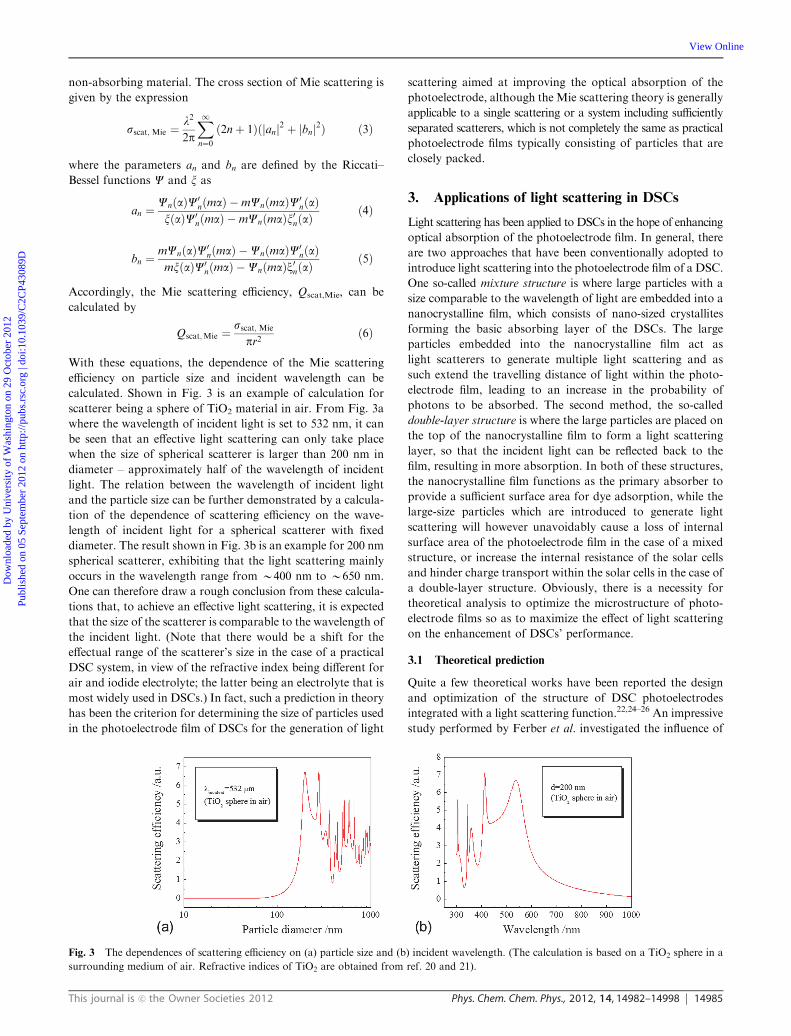
With these equations, the dependence of the Mie scattering
efficiency on particle size and incident wavelength can be
calculated. Shown in Fig. 3 is an example of calculation for
scatterer being a sphere of TiO2 material in air. From Fig. 3a
where the wavelength of incident light is set to 532 nm, it can
be seen that an effective light scattering can only take place
when the size of spherical scatterer is larger than 200 nm in
diameter – approximately half of the wavelength of incident
light. The relation between the wavelength of incident light
and the particle size can be further demonstrated by a calcula-
tion of the dependence of scattering efficiency on the wave-
length of incident light for a spherical scatterer with fixed
diameter. The result shown in Fig. 3b is an example for 200 nm
spherical scatterer, exhibiting that the light scattering mainly
occurs in the wavelength range from B400 nm to B650 nm.
One can therefore draw a rough conclusion from these calcula-
tions that, to achieve an effective light scattering, it is expected
that the size of the scatterer is comparable to the wavelength of
the incident light. (Note that there would be a shift for the
effectual range of the scatterer’s size in the case of a practical
DSC system, in view of the refractive index being different for
air and iodide electrolyte; the latter being an electrolyte that is
most widely used in DSCs.) In fact, such a prediction in theory
has been the criterion for determining the size of particles used
in the photoelectrode film of DSCs for the generation of light
scattering aimed at improving the optical absorption of the
photoelectrode, although the Mie scattering theory is generally
applicable to a single scattering or a system including sufficiently
separated scatterers, which is not completely the same as practical
photoelectrode films typically consisting of particles that are
closely packed.
3. Applications of light scattering in DSCs
Light scattering has been applied to DSCs in the hope of enhancing
optical absorption of the photoelectrode film. In general, there
are two approaches that have been conventionally adopted to
introduce light scattering into the photoelectrode film of a DSC.
One so-called mixture structure is where large particles with a
size comparable to the wavelength of light are embedded into a
nanocrystalline film, which consists of nano-sized crystallites
forming the basic absorbing layer of the DSCs. The large
particles embedded into the nanocrystalline film act as
light scatterers to generate multiple light scattering and as
such extend the travelling distance of light within the photo-
electrode film, leading to an increase in the probability of
photons to be absorbed. The second method, the so-called
double-layer structure is where the large particles are placed on
the top of the nanocrystalline film to form a light scattering
layer, so that the incident light can be reflected back to the
film, resulting in more absorption. In both of these structures,
the nanocrystalline film functions as the primary absorber to
provide a sufficient surface area for dye adsorption, while the
large-size particles which are introduced to generate light
scattering will however unavoidably cause a loss of internal
surface area of the photoelectrode film in the case of a mixed
structure, or increase the internal resistance of the solar cells
and hinder charge transport within the solar cells in the case of
a double-layer structure. Obviously, there is a necessity for
theoretical analysis to optimize the microstructure of photo-
electrode films so as to maximize the effect of light scattering
on the enhancement of DSCs’ performance.
3.1 Theoretical prediction
Quite a few theoretical works have been reported the design
and optimization of the structure of DSC photoelectrodes
integrated with a light scattering function.22,24–26 An impressive
study performed by Ferber et al. investigated the influence of
Fig. 3 The dependences of scattering efficiency on (a) particle size and (b) incident wavelength. (The calculation is based on a TiO2 sphere in a
surrounding medium of air. Refractive indices of TiO2 are obtained from ref. 20 and 21).
Dow
nloa
ded
by U
nive
rsity
of
Was
hing
ton
on 2
9 O
ctob
er 2
012
Publ
ishe
d on
05
Sept
embe
r 20
12 o
n ht
tp://
pubs
.rsc
.org
| do
i:10.
1039
/C2C
P430
89D
View Online
14986 Phys. Chem. Chem. Phys., 2012, 14, 14982–14998 This journal is c the Owner Societies 2012
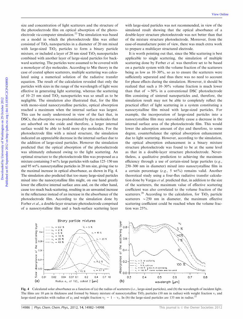
size and concentration of light scatterers and the structure of
the photoelectrode film on optical absorption of the photo-
electrode via computer simulation.22 The simulation was based
on a model in which the photoelectrode film was either
consisted of TiO2 nanoparticles in a diameter of 20 nm mixed
with large-sized TiO2 particles to form a binary particle
mixture, or included a layer of 20 nm sized TiO2 nanoparticles
combined with another layer of large-sized particles for back-
ward scattering. The particles were assumed to be covered with
a monolayer of dye molecules. According to Mie theory in the
case of coated sphere scatterers, multiple scattering was calcu-
lated using a numerical solution of the radiative transfer
equation. The result of the calculation revealed that only the
particles with sizes in the range of the wavelength of light were
effective in generating light scattering, whereas the scattering
of 10–25 nm sized TiO2 nanoparticles was so small as to be
negligible. The simulation also illustrated that, for the film
with mono-sized nanocrystalline particles, optical absorption
reached a maximum when the internal surface was largest.
This can be easily understood in view of the fact that, in
DSCs, the absorption was predominated by dye molecules that
are adsorbed on the oxide and therefore, a larger internal
surface would be able to hold more dye molecules. For the
photoelectrode film with a mixed structure, the simulation
indicated an appreciable decrease in the internal surface due to
the addition of large-sized particles. However the simulation
predicted that the optical absorption of the photoelectrode
was ultimately enhanced owing to the light scattering. An
optimal structure to the photoelectrode film was proposed as a
mixture containing 5 wt% large particles with radius 125–150 nm
and 95 wt% nanocrystalline particles in 20 nm size, giving rise to
the maximal increase in optical absorbance, as shown in Fig. 4.
The simulation also predicted that too many large-sized particles
mixed into the nanocrystalline film might, on one hand greatly
lower the effective internal surface area and, on the other hand,
cause too much back-scattering, resulting in an unwanted increase
in the reflectance instead of an increase in the absorbance of the
photoelectrode film. According to the simulation done by
Ferber et al., a double-layer structure photoelectrode comprised
of a nanocrystalline film and a back-surface scattering layer
with large-sized particles was not recommended, in view of the
simulated result showing that the optical absorbance of a
double-layer structure photoelectrode was not better than that
of the mixture structure photoelectrode. Moreover, from the
ease-of-manufacture point of view, there was much extra work
to prepare a multilayer structured electrode.
It is worth pointing out that, since the Mie scattering is best
applicable to single scattering, the simulation of multiple
scattering done by Ferber et al. was therefore set to be based
on a particle system with the volume fraction of the scatterers
being as low as 10–30%, so as to ensure the scatterers were
sufficiently separated and thus there was no need to account
for phase effects during the simulation. However, it should be
realized that such a 10–30% volume fraction is much lower
than that of B50% in a conventional DSC photoelectrode
film consisting of sintered nanoparticles and, therefore, the
simulation result may not be able to completely reflect the
practical effect of light scattering in a system constituting a
nanocrystalline film mixed with large-sized particles. For
example, the incorporation of large-sized particles into a
nanocrystalline film may unavoidably cause a decrease in the
internal surface area of the photoelectrode film. This would
lower the adsorption amount of dye and therefore, to some
degree, counterbalance the optical absorption enhancement
due to light scattering. However, according to the simulation,
the optical absorption enhancement in a binary mixture
structure photoelectrode was found to be at the same level
as that in a double-layer structure photoelectrode. Never-
theless, a qualitative prediction to achieving the maximum
efficiency through a use of certain-sized large particles (e.g.,
250–300 nm in diameter) mixed into nanocrystalline film in
a certain percentage (e.g., 5 wt%) remains valid. Another
theoretical study using a four-flux radiative transfer calcula-
tion done by Vargas et al. predicted that, in addition to the size
of the scatterers, the maximum value of effective scattering
coefficient was also correlated to the volume fraction of the
scatterers.28 According to the calculation, for TiO2 particle
scatterers B250 nm in diameter, the maximum effective
scattering coefficient could be reached when the volume frac-
tion was 25%.
Fig. 4 Calculated solar absorbance as a function of (a) the radius of scatterers (i.e., large-sized particles), and (b) the wavelength of incident light.
The films are 10 mm in thickness and formed by binary mixture of nanocrystalline TiO2 particles (10 nm in radius) with weight fraction v1 and
large-sized particles with radius of a2 and weight fraction v2 = 1 � v1. In (b) the large-sized particles are 135 nm in radius.22
Dow
nloa
ded
by U
nive
rsity
of
Was
hing
ton
on 2
9 O
ctob
er 2
012
Publ
ishe
d on
05
Sept
embe
r 20
12 o
n ht
tp://
pubs
.rsc
.org
| do
i:10.
1039
/C2C
P430
89D
View Online
This journal is c the Owner Societies 2012 Phys. Chem. Chem. Phys., 2012, 14, 14982–14998 14987
Using the theoretical model same as what was adopted by
Ferber et al., Usami also performed a systematic theoretical
study regarding the light scattering effect in DSC photoelec-
trode films with a multiple-layer structure, with the aim of
enhancing optical confinement by including an extra layer for
light reflection.23 Based on the computer simulation results, it
was proposed that an optimal DSC photoelectrode film should
be a three layer structure that consisted of a layer of conven-
tional TiO2 nanocrystalline film, a layer of large-sized TiO2
particles deposited on the top of the nanocrystalline film for
light scattering, and a thin layer of rutile TiO2 film inserted
between the nanocrystalline film and the glass substrate for
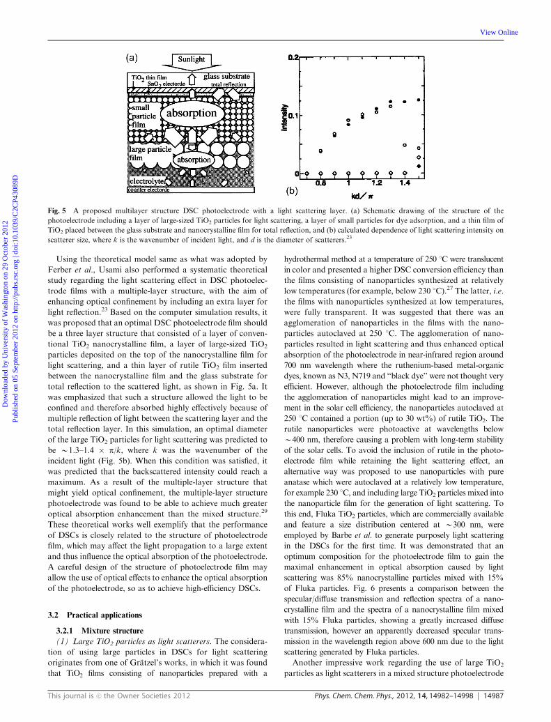
total reflection to the scattered light, as shown in Fig. 5a. It
was emphasized that such a structure allowed the light to be
confined and therefore absorbed highly effectively because of
multiple reflection of light between the scattering layer and the
total reflection layer. In this simulation, an optimal diameter
of the large TiO2 particles for light scattering was predicted to
be B1.3–1.4 � p/k, where k was the wavenumber of the
incident light (Fig. 5b). When this condition was satisfied, it
was predicted that the backscattered intensity could reach a
maximum. As a result of the multiple-layer structure that
might yield optical confinement, the multiple-layer structure
photoelectrode was found to be able to achieve much greater
optical absorption enhancement than the mixed structure.29
These theoretical works well exemplify that the performance
of DSCs is closely related to the structure of photoelectrode
film, which may affect the light propagation to a large extent
and thus influence the optical absorption of the photoelectrode.
A careful design of the structure of photoelectrode film may
allow the use of optical effects to enhance the optical absorption
of the photoelectrode, so as to achieve high-efficiency DSCs.
3.2 Practical applications
3.2.1 Mixture structure
(1) Large TiO2 particles as light scatterers. The considera-
tion of using large particles in DSCs for light scattering
originates from one of Gratzel’s works, in which it was found
that TiO2 films consisting of nanoparticles prepared with a
hydrothermal method at a temperature of 250 1C were translucent
in color and presented a higher DSC conversion efficiency than
the films consisting of nanoparticles synthesized at relatively
low temperatures (for example, below 230 1C).27 The latter, i.e.
the films with nanoparticles synthesized at low temperatures,
were fully transparent. It was suggested that there was an
agglomeration of nanoparticles in the films with the nano-
particles autoclaved at 250 1C. The agglomeration of nano-
particles resulted in light scattering and thus enhanced optical
absorption of the photoelectrode in near-infrared region around
700 nm wavelength where the ruthenium-based metal-organic
dyes, known as N3, N719 and ‘‘black dye’’ were not thought very
efficient. However, although the photoelectrode film including
the agglomeration of nanoparticles might lead to an improve-
ment in the solar cell efficiency, the nanoparticles autoclaved at
250 1C contained a portion (up to 30 wt%) of rutile TiO2. The
rutile nanoparticles were photoactive at wavelengths below
B400 nm, therefore causing a problem with long-term stability
of the solar cells. To avoid the inclusion of rutile in the photo-
electrode film while retaining the light scattering effect, an
alternative way was proposed to use nanoparticles with pure
anatase which were autoclaved at a relatively low temperature,
for example 230 1C, and including large TiO2 particles mixed into
the nanoparticle film for the generation of light scattering. To
this end, Fluka TiO2 particles, which are commercially available
and feature a size distribution centered at B300 nm, were
employed by Barbe et al. to generate purposely light scattering
in the DSCs for the first time. It was demonstrated that an
optimum composition for the photoelectrode film to gain the
maximal enhancement in optical absorption caused by light
scattering was 85% nanocrystalline particles mixed with 15%
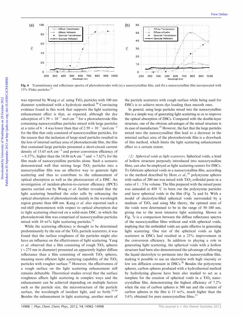
of Fluka particles. Fig. 6 presents a comparison between the
specular/diffuse transmission and reflection spectra of a nano-
crystalline film and the spectra of a nanocrystalline film mixed
with 15% Fluka particles, showing a greatly increased diffuse
transmission, however an apparently decreased specular trans-
mission in the wavelength region above 600 nm due to the light
scattering generated by Fluka particles.
Another impressive work regarding the use of large TiO2
particles as light scatterers in a mixed structure photoelectrode
Fig. 5 A proposed multilayer structure DSC photoelectrode with a light scattering layer. (a) Schematic drawing of the structure of the
photoelectrode including a layer of large-sized TiO2 particles for light scattering, a layer of small particles for dye adsorption, and a thin film of
TiO2 placed between the glass substrate and nanocrystalline film for total reflection, and (b) calculated dependence of light scattering intensity on
scatterer size, where k is the wavenumber of incident light, and d is the diameter of scatterers.23
Dow
nloa
ded
by U
nive
rsity
of
Was
hing
ton
on 2
9 O
ctob
er 2
012
Publ
ishe
d on
05
Sept
embe
r 20
12 o
n ht
tp://
pubs
.rsc
.org
| do
i:10.
1039
/C2C
P430
89D
View Online
14988 Phys. Chem. Chem. Phys., 2012, 14, 14982–14998 This journal is c the Owner Societies 2012
was reported by Wang et al. using TiO2 particles with 100 nm
diameter synthesized with a hydrolysis method.30 Convincing
evidence found in this work that supports the light scattering
enhancement effect is that, as expected, although the dye
adsorption of 1.59 � 10�7 mol cm�2 for a photoelectrode film
containing nanocrystalline particles mixed with large particles
at a ratio of 6 : 4 was lower than that of 2.59 � 10�7 mol cm�2
for the film that only consisted of nanocrystalline particles, for
the reason that the inclusion of large-sized particles resulted in
the loss of internal surface area of photoelectrode film, the film
that contained large particles presented a short-circuit current
density of 15.65 mA cm�2 and power conversion efficiency of
B8.37%, higher than the 14.86 mA cm�2 andB7.62% for the
film made of nanocrystalline particles alone. Such a scenario
demonstrated well that mixing large TiO2 particles into a
nanocrystalline film was an effective way to generate light
scattering and thus to contribute to the enhancement of
optical absorption as well as the photocurrent of a DSC. An
investigation of incident-photon-to-current efficiency (IPCE)
spectra carried out by Wang et al. further revealed that the
light scattering benefited the solar cells by enhancing the
optical absorption of photoelectrode mainly in the wavelength
region greater than 600 nm. Kang et al. also reported such a
red-shift phenomenon with respect to optical absorption due
to light scattering observed on a solid-state DSC, in which the
photoelectrode film was comprised of nanocrystalline particles
mixed with 10 wt% light scattering particles.31
While the scattering efficiency is thought to be determined
predominantly by the size of the TiO2 particle scatterers, it was
found that the surface roughness of the particles might also
have an influence on the effectiveness of light scattering. Yang
et al. observed that a film consisting of rough TiO2 spheres
(B275 nm in diameter) presented an apparently higher diffuse
reflectance than a film consisting of smooth TiO2 spheres,
meaning more efficient light scattering capability of the TiO2
particles with rougher surface.32 However, the effectiveness of
a rough surface on the light scattering enhancement still
remains debatable. Theoretical studies reveal that the surface
roughness affects light scattering in complex ways and the
enhancement can be achieved depending on multiple factors
such as the particle size, the microstructure of the particle
surface, the wavelength of incident light, and so forth.33,34
Besides the enhancement in light scattering, another merit of
the particle scatterers with rough surface while being used for
DSCs is to achieve more dye loading than smooth ones.
In general, using large particles mixed into the nanocrystalline
film is a simple way of generating light scattering so as to improve
the optical absorption of DSCs. Compared with the double-layer
structure, one of the obvious advantages of the mixed structure is
its ease of manufacture.35 However, the fact that the large particles
mixed into the nanocrystalline film lead to a decrease in the
internal surface area of the photoelectrode film is a drawback
of this method, which limits the light scattering enhancement
effect to a certain extent.
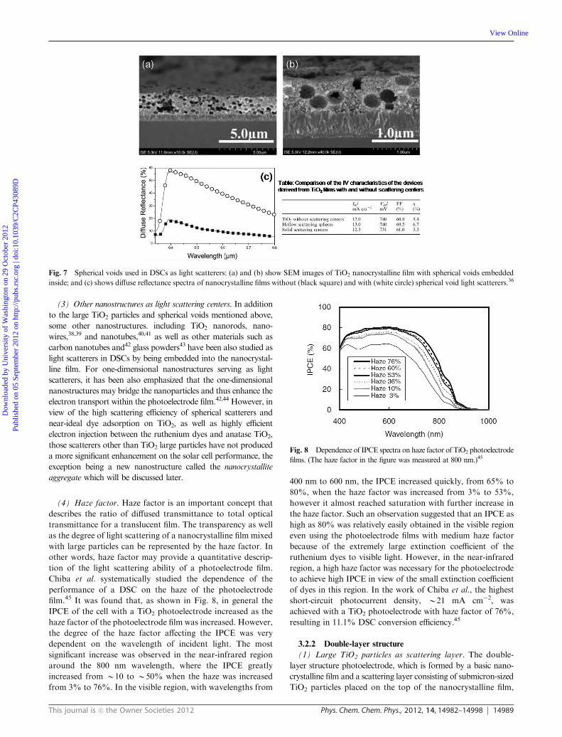
(2) Spherical voids as light scatterers. Spherical voids, a kind
of hollow structure purposely introduced into nanocrystalline
films, can also be employed as light scattering centers for DSCs.
To fabricate spherical voids in a nanocrystalline film, according
to the method described by Hore et al.,36 polystyrene spheres
with radius of 200 nm was mixed with TiO2 colloidal paste in a
ratio of 1 : 5 by volume. The film prepared with the mixed paste
was annealed at 450 1C to burn out the polystyrene particles
and leave spherical voids in the film (Fig. 7a and b). With a
model of electrolyte-filled spherical voids surrounded by a
medium of TiO2 and using Mie theory, the optimal sizes of
the voids were determined to be in the range of 50–100 nm,
giving rise to the most intensive light scattering. Shown in
Fig. 7c is a comparison between the diffuse reflectance spectra
of the nanocrystalline films without and with spherical voids,
implying that the embedded voids are quite effective in generating
light scattering. One test of the spherical voids as light
scatterers in DSCs had resulted in a 25% improvement in
the conversion efficiency. In addition to playing a role in
generating light scattering, the spherical voids with a hollow
structure had been also demonstrated the advantage of allowing
the liquid electrolyte to permeate into the nanocrystalline film,
making it possible to use an electrolyte with high viscosity or
low ion diffusion constant in DSCs.36 Besides the polystyrene
spheres, carbon spheres produced with a hydrothermal method
by hydrolyzing glucose have been also studied to act as a
template for the creation of spherical voids in a TiO2 nano-
crystalline film, demonstrating the highest efficiency of 7.2%
when the size of carbon spheres is 500 nm and the content of
carbon spheres in the film is 15 wt%, much higher than the
5.6% obtained for pure nanocrystalline films.37
Fig. 6 Transmittance and reflectance spectra of photoelectrodes with (a) a nanocrystalline film, and (b) a nanocrystalline film incorporated with
15% Fluka particles.27
Dow
nloa
ded
by U
nive
rsity
of
Was
hing
ton
on 2
9 O
ctob
er 2
012
Publ
ishe
d on
05
Sept
embe
r 20
12 o
n ht
tp://
pubs
.rsc
.org
| do
i:10.
1039
/C2C
P430
89D
View Online
This journal is c the Owner Societies 2012 Phys. Chem. Chem. Phys., 2012, 14, 14982–14998 14989
(3) Other nanostructures as light scattering centers. In addition
to the large TiO2 particles and spherical voids mentioned above,
some other nanostructures. including TiO2 nanorods, nano-
wires,38,39 and nanotubes,40,41 as well as other materials such as
carbon nanotubes and42 glass powders43 have been also studied as
light scatterers in DSCs by being embedded into the nanocrystal-
line film. For one-dimensional nanostructures serving as light
scatterers, it has been also emphasized that the one-dimensional
nanostructures may bridge the nanoparticles and thus enhance the
electron transport within the photoelectrode film.42,44 However, in
view of the high scattering efficiency of spherical scatterers and
near-ideal dye adsorption on TiO2, as well as highly efficient
electron injection between the ruthenium dyes and anatase TiO2,
those scatterers other than TiO2 large particles have not produced
a more significant enhancement on the solar cell performance, the
exception being a new nanostructure called the nanocrystallite
aggregate which will be discussed later.
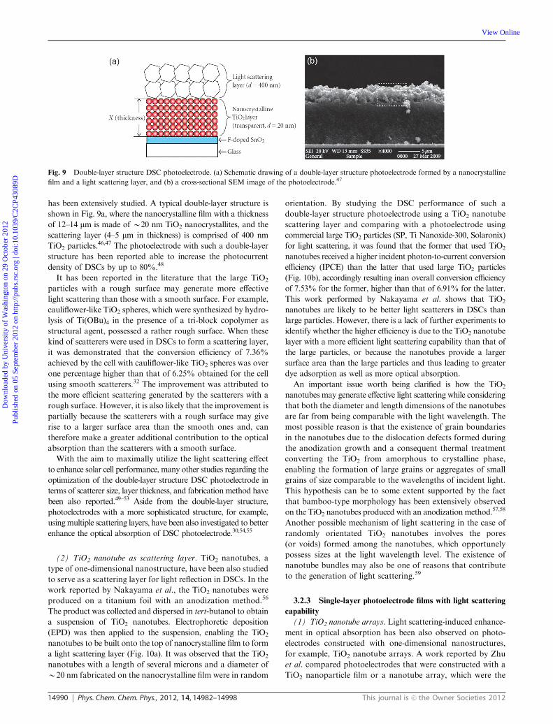
(4) Haze factor. Haze factor is an important concept that
describes the ratio of diffused transmittance to total optical
transmittance for a translucent film. The transparency as well
as the degree of light scattering of a nanocrystalline film mixed
with large particles can be represented by the haze factor. In
other words, haze factor may provide a quantitative descrip-
tion of the light scattering ability of a photoelectrode film.
Chiba et al. systematically studied the dependence of the
performance of a DSC on the haze of the photoelectrode
film.45 It was found that, as shown in Fig. 8, in general the
IPCE of the cell with a TiO2 photoelectrode increased as the
haze factor of the photoelectrode film was increased. However,
the degree of the haze factor affecting the IPCE was very
dependent on the wavelength of incident light. The most
significant increase was observed in the near-infrared region
around the 800 nm wavelength, where the IPCE greatly
increased from B10 to B50% when the haze was increased
from 3% to 76%. In the visible region, with wavelengths from
400 nm to 600 nm, the IPCE increased quickly, from 65% to
80%, when the haze factor was increased from 3% to 53%,
however it almost reached saturation with further increase in
the haze factor. Such an observation suggested that an IPCE as
high as 80% was relatively easily obtained in the visible region
even using the photoelectrode films with medium haze factor
because of the extremely large extinction coefficient of the
ruthenium dyes to visible light. However, in the near-infrared
region, a high haze factor was necessary for the photoelectrode
to achieve high IPCE in view of the small extinction coefficient
of dyes in this region. In the work of Chiba et al., the highest
short-circuit photocurrent density, B21 mA cm�2, was
achieved with a TiO2 photoelectrode with haze factor of 76%,
resulting in 11.1% DSC conversion efficiency.45
3.2.2 Double-layer structure
(1) Large TiO2 particles as scattering layer. The double-
layer structure photoelectrode, which is formed by a basic nano-
crystalline film and a scattering layer consisting of submicron-sized
TiO2 particles placed on the top of the nanocrystalline film,
Fig. 7 Spherical voids used in DSCs as light scatterers: (a) and (b) show SEM images of TiO2 nanocrystalline film with spherical voids embedded
inside; and (c) shows diffuse reflectance spectra of nanocrystalline films without (black square) and with (white circle) spherical void light scatterers.36
Fig. 8 Dependence of IPCE spectra on haze factor of TiO2 photoelectrode
films. (The haze factor in the figure was measured at 800 nm.)45
Dow
nloa
ded
by U
nive
rsity
of
Was
hing
ton
on 2
9 O
ctob
er 2
012
Publ
ishe
d on
05
Sept
embe
r 20
12 o
n ht
tp://
pubs
.rsc
.org
| do
i:10.
1039
/C2C
P430
89D
View Online
14990 Phys. Chem. Chem. Phys., 2012, 14, 14982–14998 This journal is c the Owner Societies 2012
has been extensively studied. A typical double-layer structure is
shown in Fig. 9a, where the nanocrystalline film with a thickness
of 12–14 mm is made of B20 nm TiO2 nanocrystallites, and the
scattering layer (4–5 mm in thickness) is comprised of 400 nm
TiO2 particles.46,47 The photoelectrode with such a double-layer
structure has been reported able to increase the photocurrent
density of DSCs by up to 80%.48
It has been reported in the literature that the large TiO2
particles with a rough surface may generate more effective
light scattering than those with a smooth surface. For example,
cauliflower-like TiO2 spheres, which were synthesized by hydro-
lysis of Ti(OBu)4 in the presence of a tri-block copolymer as
structural agent, possessed a rather rough surface. When these
kind of scatterers were used in DSCs to form a scattering layer,
it was demonstrated that the conversion efficiency of 7.36%
achieved by the cell with cauliflower-like TiO2 spheres was over
one percentage higher than that of 6.25% obtained for the cell
using smooth scatterers.32 The improvement was attributed to
the more efficient scattering generated by the scatterers with a
rough surface. However, it is also likely that the improvement is
partially because the scatterers with a rough surface may give
rise to a larger surface area than the smooth ones and, can
therefore make a greater additional contribution to the optical
absorption than the scatterers with a smooth surface.
With the aim to maximally utilize the light scattering effect
to enhance solar cell performance, many other studies regarding the
optimization of the double-layer structure DSC photoelectrode in
terms of scatterer size, layer thickness, and fabrication method have
been also reported.49–53 Aside from the double-layer structure,
photoelectrodes with a more sophisticated structure, for example,
usingmultiple scattering layers, have been also investigated to better
enhance the optical absorption of DSC photoelectrode.30,54,55
(2) TiO2 nanotube as scattering layer. TiO2 nanotubes, a
type of one-dimensional nanostructure, have been also studied
to serve as a scattering layer for light reflection in DSCs. In the
work reported by Nakayama et al., the TiO2 nanotubes were
produced on a titanium foil with an anodization method.56
The product was collected and dispersed in tert-butanol to obtain
a suspension of TiO2 nanotubes. Electrophoretic deposition
(EPD) was then applied to the suspension, enabling the TiO2
nanotubes to be built onto the top of nanocrystalline film to form
a light scattering layer (Fig. 10a). It was observed that the TiO2
nanotubes with a length of several microns and a diameter of
B20 nm fabricated on the nanocrystalline film were in random
orientation. By studying the DSC performance of such a
double-layer structure photoelectrode using a TiO2 nanotube
scattering layer and comparing with a photoelectrode using
commercial large TiO2 particles (SP, Ti Nanoxide-300, Solaronix)
for light scattering, it was found that the former that used TiO2
nanotubes received a higher incident photon-to-current conversion
efficiency (IPCE) than the latter that used large TiO2 particles
(Fig. 10b), accordingly resulting inan overall conversion efficiency
of 7.53% for the former, higher than that of 6.91% for the latter.
This work performed by Nakayama et al. shows that TiO2
nanotubes are likely to be better light scatterers in DSCs than
large particles. However, there is a lack of further experiments to
identify whether the higher efficiency is due to the TiO2 nanotube
layer with a more efficient light scattering capability than that of
the large particles, or because the nanotubes provide a larger
surface area than the large particles and thus leading to greater
dye adsorption as well as more optical absorption.
An important issue worth being clarified is how the TiO2
nanotubes may generate effective light scattering while considering
that both the diameter and length dimensions of the nanotubes
are far from being comparable with the light wavelength. The
most possible reason is that the existence of grain boundaries
in the nanotubes due to the dislocation defects formed during
the anodization growth and a consequent thermal treatment
converting the TiO2 from amorphous to crystalline phase,
enabling the formation of large grains or aggregates of small
grains of size comparable to the wavelengths of incident light.
This hypothesis can be to some extent supported by the fact
that bamboo-type morphology has been extensively observed
on the TiO2 nanotubes produced with an anodization method.57,58
Another possible mechanism of light scattering in the case of
randomly orientated TiO2 nanotubes involves the pores
(or voids) formed among the nanotubes, which opportunely
possess sizes at the light wavelength level. The existence of
nanotube bundles may also be one of reasons that contribute
to the generation of light scattering.59
3.2.3 Single-layer photoelectrode films with light scattering
capability
(1) TiO2 nanotube arrays. Light scattering-induced enhance-
ment in optical absorption has been also observed on photo-
electrodes constructed with one-dimensional nanostructures,
for example, TiO2 nanotube arrays. A work reported by Zhu
et al. compared photoelectrodes that were constructed with a
TiO2 nanoparticle film or a nanotube array, which were the
Fig. 9 Double-layer structure DSC photoelectrode. (a) Schematic drawing of a double-layer structure photoelectrode formed by a nanocrystalline
film and a light scattering layer, and (b) a cross-sectional SEM image of the photoelectrode.47
Dow
nloa
ded
by U
nive
rsity
of
Was
hing
ton
on 2
9 O
ctob
er 2
012
Publ
ishe
d on
05
Sept
embe
r 20
12 o
n ht
tp://
pubs
.rsc
.org
| do
i:10.
1039
/C2C
P430
89D
View Online
This journal is c the Owner Societies 2012 Phys. Chem. Chem. Phys., 2012, 14, 14982–14998 14991
same in thickness.60 Besides the advantage of nanotubes that
could provide direct pathways for electron transport, which
led to a charge recombination in the nanotube array 10 times
lower than that in the nanoparticle film, it was found that light
harvesting efficiency of the nanotube photoelectrode was at
least 20% higher than that of the nanoparticle photoelectrode
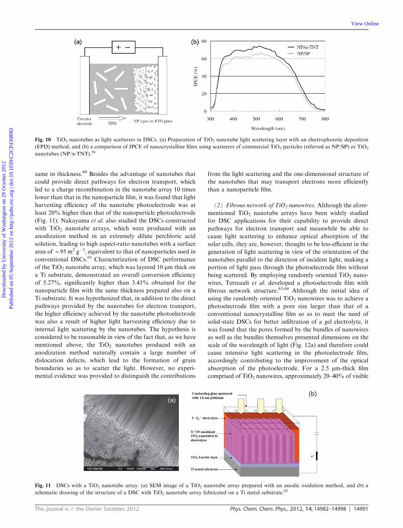
(Fig. 11). Nakayama et al. also studied the DSCs constructed
with TiO2 nanotube arrays, which were produced with an
anodization method in an extremely dilute perchloric acid
solution, leading to high aspect-ratio nanotubes with a surface
area ofB95 m2 g�1, equivalent to that of nanoparticles used in
conventional DSCs.61 Characterization of DSC performance
of the TiO2 nanotube array, which was layered 10 mm thick on
a Ti substrate, demonstrated an overall conversion efficiency
of 5.27%, significantly higher than 3.41% obtained for the
nanoparticle film with the same thickness prepared also on a
Ti substrate. It was hypothesized that, in addition to the direct
pathways provided by the nanotubes for electron transport,
the higher efficiency achieved by the nanotube photoelectrode
was also a result of higher light harvesting efficiency due to
internal light scattering by the nanotubes. The hypothesis is
considered to be reasonable in view of the fact that, as we have
mentioned above, the TiO2 nanotubes produced with an
anodization method naturally contain a large number of
dislocation defects, which lead to the formation of grain
boundaries so as to scatter the light. However, no experi-
mental evidence was provided to distinguish the contributions
from the light scattering and the one-dimensional structure of
the nanotubes that may transport electrons more efficiently
than a nanoparticle film.
(2) Fibrous network of TiO2 nanowires. Although the afore-
mentioned TiO2 nanotube arrays have been widely studied
for DSC applications for their capability to provide direct
pathways for electron transport and meanwhile be able to
cause light scattering to enhance optical absorption of the
solar cells, they are, however, thought to be less-efficient in the
generation of light scattering in view of the orientation of the
nanotubes parallel to the direction of incident light, making a
portion of light pass through the photoelectrode film without
being scattered. By employing randomly oriented TiO2 nano-
wires, Tetreault et al. developed a photoelectrode film with
fibrous network structure.63,64 Although the initial idea of
using the randomly oriented TiO2 nanowires was to achieve a
photoelectrode film with a pore size larger than that of a
conventional nanocrystalline film so as to meet the need of
solid-state DSCs for better infiltration of a gel electrolyte, it
was found that the pores formed by the bundles of nanowires
as well as the bundles themselves presented dimensions on the
scale of the wavelength of light (Fig. 12a) and therefore could
cause intensive light scattering in the photoelectrode film,
accordingly contributing to the improvement of the optical
absorption of the photoelectrode. For a 2.5 mm-thick film
comprised of TiO2 nanowires, approximately 20–40% of visible
Fig. 10 TiO2 nanotubes as light scatterers in DSCs. (a) Preparation of TiO2 nanotube light scattering layer with an electrophoretic deposition
(EPD) method, and (b) a comparison of IPCE of nanocrystalline films using scatterers of commercial TiO2 particles (referred as NP/SP) or TiO2
nanotubes (NP/a-TNT).56
Fig. 11 DSCs with a TiO2 nanotube array. (a) SEM image of a TiO2 nanotube array prepared with an anodic oxidation method, and (b) a
schematic drawing of the structure of a DSC with TiO2 nanotube array fabricated on a Ti metal substrate.62
Dow
nloa
ded
by U
nive
rsity
of
Was
hing
ton
on 2
9 O
ctob
er 2
012
Publ
ishe
d on
05
Sept
embe
r 20
12 o
n ht
tp://
pubs
.rsc
.org
| do
i:10.
1039
/C2C
P430
89D
View Online
14992 Phys. Chem. Chem. Phys., 2012, 14, 14982–14998 This journal is c the Owner Societies 2012
light was found to be scattered by transmission and reflection
(Fig. 12b). Besides the merit of being more efficient in light
scattering than a nanotube array, the randomly oriented
nanowires forming the photoelectrode film of a DSC may also
provide benefit in making easier the manufacture of photo-
electrodes for DSCs.
(3) Submicron sized TiO2 hollow spheres. Submicron sized
TiO2 hollow spheres are also a structure that can generate
highly effective light scattering and, when used in DSCs, they
have been reported able to achieve a conversion efficiency
comparable to those of conventional photoelectrodes made of
a nanocrystalline film.65 TiO2 hollow spheres can be prepared
with a template method using spherical polystyrene (PS), which is
removed in a sequential sintering treatment. The TiO2 spheres
synthesized with this method typically feature a hollow structure
with a diameter of 400–500 nm and a shell thickness of 30 nm
(Fig. 13). In the work performed by Park et al., the DSC
performance of a photoelectrode film consisting ofB12 mm-thick
TiO2 hollow spheres was studied.65 It was found that the amount
of dye adsorbed on the photoelectrode film of TiO2 hollow spheres
was only about one-third of that on a nanocrystalline film,
however the DSC conversion efficiency of 4.3% received by the
hollow sphere photoelectrode was almost 87% of the 4.95%
efficiency obtained for the nanocrystalline film. It was inferred
that light scattering generated by the hollow spheres had
contributed to the optical absorption and greatly improved
the light harvesting efficiency of the photoelectrode.
Multilayered hollow spheres have also been studied for
application to DSCs. Compared with single-shelled hollow
spheres, the multilayered hollow spheres have the apparent advan-
tage of providing larger specific surface area for dye adsorption.
Regarding optical behavior, Qian et al.66 andWu et al.67 suggested
that the multilayered hollow spheres might yield more effective
light scattering than the single-shelled hollow spheres due to the
existence of multiple layers which led to multiple light scattering
and, possibly, optical localization within the spheres. More
importantly, in view of the inner spheres having varying sizes,
the light scattering could happen in a broader wavelength range
than what single-shelled hollow spheres did (Fig. 14). In the work
carried out by Qian et al., the DSC with TiO2-coated multilayered
SnO2 hollow spheres demonstrated an efficiency of 5.65%, higher
than 5.14% obtained for TiO2 nanocrystalline film (P25) with the
same thickness,B10 mm.66 In another work reported byWu et al.,
multilayered TiO2 hollow spheres comprising a DSC photoelec-
trode film did not however show better efficiency than the TiO2
nanocrystalline film (P25), but their action as a light scattering
layer was shown to be able to significantly increase the optical
absorption, leading to an impressively high efficiency ofB9.1%.67
These results verify that the hollow spheres, especially the multi-
layered hollow spheres, are promisingmaterial with light scattering
capability for DSC application. However, the structure of them in
terms of the size of the spheres and inner cavities, the thickness of
each layer, and the number of layers is anticipated to be further
optimized to maximize the dye loading and the multiple
light scattering effect. A recently published review paper well
summarized the existing methods for the synthesis of hollow
structured spheres.68
(4) Multifunctional 3D nanostructures. While light scattering
is purposely introduced into DSCs to enhance light harvesting,
recently some three-dimensional (3D) nanostructures have been
developed to fulfil multiple functions. These 3D nanostructures
may not only bring about light scattering, but may also benefit
the solar cells by providing other functions, such as offering large
internal surface area for sufficient dye loading, or forming an
internally connected core–shell structure to reduce the charge
recombination in DSCs. Two typical multifunctional 3D nano
structures designed for enhancing the performance of DSCs in
these regards are (a) spherical aggregates of oxide nanocrystal-
lites, and (b) host–passivation–guest (H–P–G) structure.
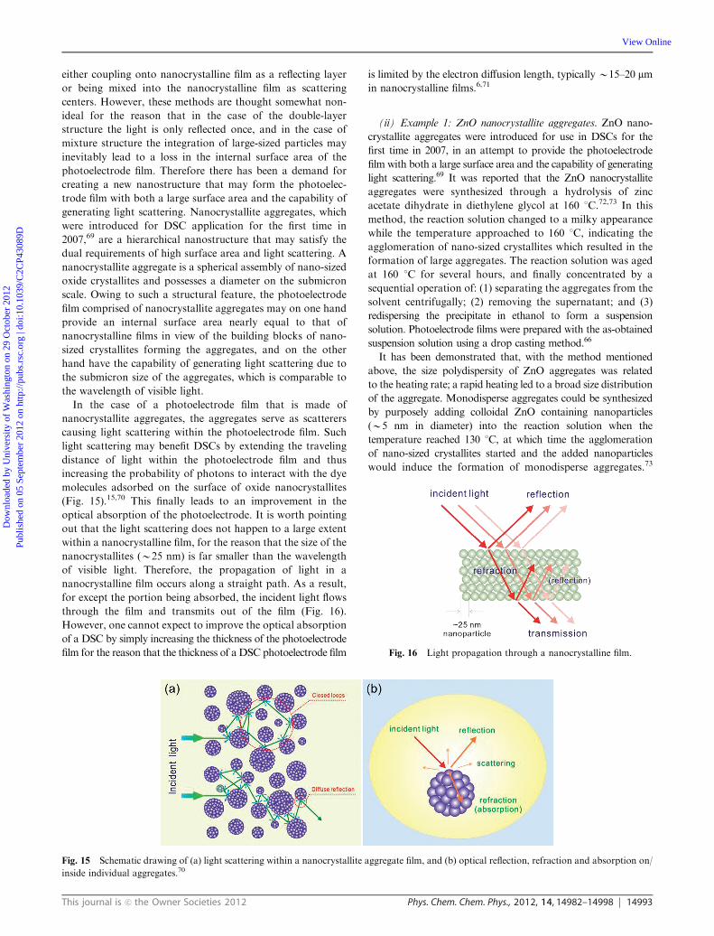
I. Spherical aggregates of oxide nanocrystallites
(i) Principle. As discussed above, large-sized oxide particles
have been widely used to generate light scattering in DSCs by
Fig. 12 Fibrous network structure photoelectrode consisting of TiO2
nanowires. (a) SEM image, and (b) transmittance and reflectance
spectra of the photoelectrode film.63
Fig. 13 TiO2 hollow spheres. (a) SEM image, and (b) TEM image.65
Fig. 14 TiO2-coated SnO2 multilayered hollow spheres (TiO2–SnO2
MHSs) demonstrating high DSC efficiency. The inset schematically
shows multiple light scattering within a multilayered hollow sphere.66
Dow
nloa
ded
by U
nive
rsity
of
Was
hing
ton
on 2
9 O
ctob
er 2
012
Publ
ishe
d on
05
Sept
embe
r 20
12 o
n ht
tp://
pubs
.rsc
.org
| do
i:10.
1039
/C2C
P430
89D
View Online
This journal is c the Owner Societies 2012 Phys. Chem. Chem. Phys., 2012, 14, 14982–14998 14993
either coupling onto nanocrystalline film as a reflecting layer
or being mixed into the nanocrystalline film as scattering
centers. However, these methods are thought somewhat non-
ideal for the reason that in the case of the double-layer
structure the light is only reflected once, and in the case of
mixture structure the integration of large-sized particles may
inevitably lead to a loss in the internal surface area of the
photoelectrode film. Therefore there has been a demand for
creating a new nanostructure that may form the photoelec-
trode film with both a large surface area and the capability of
generating light scattering. Nanocrystallite aggregates, which
were introduced for DSC application for the first time in
2007,69 are a hierarchical nanostructure that may satisfy the
dual requirements of high surface area and light scattering. A
nanocrystallite aggregate is a spherical assembly of nano-sized
oxide crystallites and possesses a diameter on the submicron
scale. Owing to such a structural feature, the photoelectrode
film comprised of nanocrystallite aggregates may on one hand
provide an internal surface area nearly equal to that of
nanocrystalline films in view of the building blocks of nano-
sized crystallites forming the aggregates, and on the other
hand have the capability of generating light scattering due to
the submicron size of the aggregates, which is comparable to
the wavelength of visible light.
In the case of a photoelectrode film that is made of
nanocrystallite aggregates, the aggregates serve as scatterers
causing light scattering within the photoelectrode film. Such
light scattering may benefit DSCs by extending the traveling
distance of light within the photoelectrode film and thus
increasing the probability of photons to interact with the dye
molecules adsorbed on the surface of oxide nanocrystallites
(Fig. 15).15,70 This finally leads to an improvement in the
optical absorption of the photoelectrode. It is worth pointing
out that the light scattering does not happen to a large extent
within a nanocrystalline film, for the reason that the size of the
nanocrystallites (B25 nm) is far smaller than the wavelength
of visible light. Therefore, the propagation of light in a
nanocrystalline film occurs along a straight path. As a result,
for except the portion being absorbed, the incident light flows
through the film and transmits out of the film (Fig. 16).
However, one cannot expect to improve the optical absorption
of a DSC by simply increasing the thickness of the photoelectrode
film for the reason that the thickness of a DSC photoelectrode film
is limited by the electron diffusion length, typicallyB15–20 mmin nanocrystalline films.6,71
(ii) Example 1: ZnO nanocrystallite aggregates. ZnO nano-
crystallite aggregates were introduced for use in DSCs for the
first time in 2007, in an attempt to provide the photoelectrode
film with both a large surface area and the capability of generating
light scattering.69 It was reported that the ZnO nanocrystallite
aggregates were synthesized through a hydrolysis of zinc
acetate dihydrate in diethylene glycol at 160 1C.72,73 In this
method, the reaction solution changed to a milky appearance
while the temperature approached to 160 1C, indicating the
agglomeration of nano-sized crystallites which resulted in the
formation of large aggregates. The reaction solution was aged
at 160 1C for several hours, and finally concentrated by a
sequential operation of: (1) separating the aggregates from the
solvent centrifugally; (2) removing the supernatant; and (3)
redispersing the precipitate in ethanol to form a suspension
solution. Photoelectrode films were prepared with the as-obtained
suspension solution using a drop casting method.66
It has been demonstrated that, with the method mentioned
above, the size polydispersity of ZnO aggregates was related
to the heating rate; a rapid heating led to a broad size distribution
of the aggregate. Monodisperse aggregates could be synthesized
by purposely adding colloidal ZnO containing nanoparticles
(B5 nm in diameter) into the reaction solution when the
temperature reached 130 1C, at which time the agglomeration
of nano-sized crystallites started and the added nanoparticles
would induce the formation of monodisperse aggregates.73
Fig. 15 Schematic drawing of (a) light scattering within a nanocrystallite aggregate film, and (b) optical reflection, refraction and absorption on/
inside individual aggregates.70
Fig. 16 Light propagation through a nanocrystalline film.
Dow
nloa
ded
by U
nive
rsity
of
Was
hing
ton
on 2
9 O
ctob
er 2
012
Publ
ishe
d on
05
Sept
embe
r 20
12 o
n ht
tp://
pubs
.rsc
.org
| do
i:10.
1039
/C2C
P430
89D
View Online
14994 Phys. Chem. Chem. Phys., 2012, 14, 14982–14998 This journal is c the Owner Societies 2012
The size of resultant aggregates could be adjusted by the amount
of colloidal ZnO that was added into the reaction solution.
Generally, more colloidal ZnO would lead to smaller aggregates.
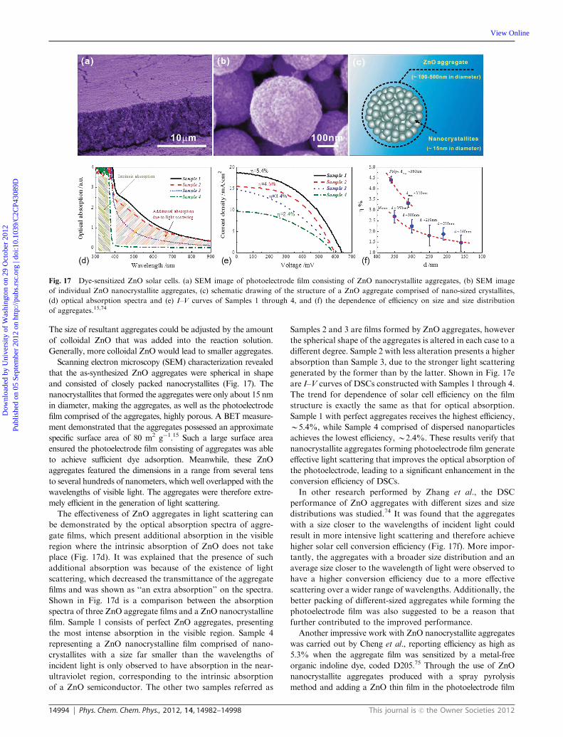
Scanning electron microscopy (SEM) characterization revealed
that the as-synthesized ZnO aggregates were spherical in shape
and consisted of closely packed nanocrystallites (Fig. 17). The
nanocrystallites that formed the aggregates were only about 15 nm
in diameter, making the aggregates, as well as the photoelectrode
film comprised of the aggregates, highly porous. A BET measure-
ment demonstrated that the aggregates possessed an approximate
specific surface area of 80 m2 g�1.15 Such a large surface area
ensured the photoelectrode film consisting of aggregates was able
to achieve sufficient dye adsorption. Meanwhile, these ZnO
aggregates featured the dimensions in a range from several tens
to several hundreds of nanometers, which well overlapped with the
wavelengths of visible light. The aggregates were therefore extre-
mely efficient in the generation of light scattering.
The effectiveness of ZnO aggregates in light scattering can
be demonstrated by the optical absorption spectra of aggre-
gate films, which present additional absorption in the visible
region where the intrinsic absorption of ZnO does not take
place (Fig. 17d). It was explained that the presence of such
additional absorption was because of the existence of light
scattering, which decreased the transmittance of the aggregate
films and was shown as ‘‘an extra absorption’’ on the spectra.
Shown in Fig. 17d is a comparison between the absorption
spectra of three ZnO aggregate films and a ZnO nanocrystalline
film. Sample 1 consists of perfect ZnO aggregates, presenting
the most intense absorption in the visible region. Sample 4
representing a ZnO nanocrystalline film comprised of nano-
crystallites with a size far smaller than the wavelengths of
incident light is only observed to have absorption in the near-
ultraviolet region, corresponding to the intrinsic absorption
of a ZnO semiconductor. The other two samples referred as
Samples 2 and 3 are films formed by ZnO aggregates, however
the spherical shape of the aggregates is altered in each case to a
different degree. Sample 2 with less alteration presents a higher
absorption than Sample 3, due to the stronger light scattering
generated by the former than by the latter. Shown in Fig. 17e
are I–V curves of DSCs constructed with Samples 1 through 4.
The trend for dependence of solar cell efficiency on the film
structure is exactly the same as that for optical absorption.
Sample 1 with perfect aggregates receives the highest efficiency,
B5.4%, while Sample 4 comprised of dispersed nanoparticles
achieves the lowest efficiency, B2.4%. These results verify that
nanocrystallite aggregates forming photoelectrode film generate
effective light scattering that improves the optical absorption of
the photoelectrode, leading to a significant enhancement in the
conversion efficiency of DSCs.
In other research performed by Zhang et al., the DSC
performance of ZnO aggregates with different sizes and size
distributions was studied.74 It was found that the aggregates
with a size closer to the wavelengths of incident light could
result in more intensive light scattering and therefore achieve
higher solar cell conversion efficiency (Fig. 17f). More impor-
tantly, the aggregates with a broader size distribution and an
average size closer to the wavelength of light were observed to
have a higher conversion efficiency due to a more effective
scattering over a wider range of wavelengths. Additionally, the
better packing of different-sized aggregates while forming the
photoelectrode film was also suggested to be a reason that
further contributed to the improved performance.
Another impressive work with ZnO nanocrystallite aggregates
was carried out by Cheng et al., reporting efficiency as high as
5.3% when the aggregate film was sensitized by a metal-free
organic indoline dye, coded D205.75 Through the use of ZnO
nanocrystallite aggregates produced with a spray pyrolysis
method and adding a ZnO thin film in the photoelectrode film
Fig. 17 Dye-sensitized ZnO solar cells. (a) SEM image of photoelectrode film consisting of ZnO nanocrystallite aggregates, (b) SEM image
of individual ZnO nanocrystallite aggregates, (c) schematic drawing of the structure of a ZnO aggregate comprised of nano-sized crystallites,
(d) optical absorption spectra and (e) I–V curves of Samples 1 through 4, and (f) the dependence of efficiency on size and size distribution
of aggregates.15,74
Dow
nloa
ded
by U
nive
rsity
of
Was
hing
ton
on 2
9 O
ctob
er 2
012
Publ
ishe
d on
05
Sept
embe
r 20
12 o
n ht
tp://
pubs
.rsc
.org
| do
i:10.
1039
/C2C
P430
89D
View Online
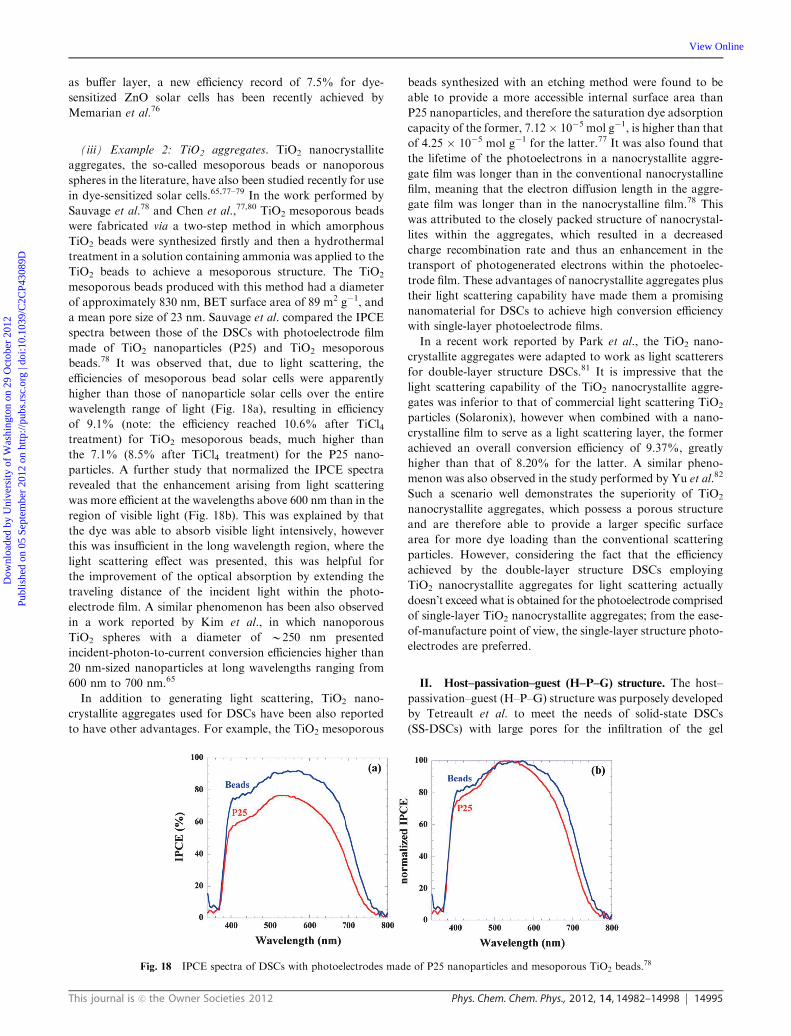
This journal is c the Owner Societies 2012 Phys. Chem. Chem. Phys., 2012, 14, 14982–14998 14995
as buffer layer, a new efficiency record of 7.5% for dye-
sensitized ZnO solar cells has been recently achieved by
Memarian et al.76
(iii) Example 2: TiO2 aggregates. TiO2 nanocrystallite
aggregates, the so-called mesoporous beads or nanoporous
spheres in the literature, have also been studied recently for use
in dye-sensitized solar cells.65,77–79 In the work performed by
Sauvage et al.78 and Chen et al.,77,80 TiO2 mesoporous beads
were fabricated via a two-step method in which amorphous
TiO2 beads were synthesized firstly and then a hydrothermal
treatment in a solution containing ammonia was applied to the
TiO2 beads to achieve a mesoporous structure. The TiO2
mesoporous beads produced with this method had a diameter
of approximately 830 nm, BET surface area of 89 m2 g�1, and
a mean pore size of 23 nm. Sauvage et al. compared the IPCE
spectra between those of the DSCs with photoelectrode film
made of TiO2 nanoparticles (P25) and TiO2 mesoporous
beads.78 It was observed that, due to light scattering, the
efficiencies of mesoporous bead solar cells were apparently
higher than those of nanoparticle solar cells over the entire
wavelength range of light (Fig. 18a), resulting in efficiency
of 9.1% (note: the efficiency reached 10.6% after TiCl4treatment) for TiO2 mesoporous beads, much higher than
the 7.1% (8.5% after TiCl4 treatment) for the P25 nano-
particles. A further study that normalized the IPCE spectra
revealed that the enhancement arising from light scattering
was more efficient at the wavelengths above 600 nm than in the
region of visible light (Fig. 18b). This was explained by that
the dye was able to absorb visible light intensively, however
this was insufficient in the long wavelength region, where the
light scattering effect was presented, this was helpful for
the improvement of the optical absorption by extending the
traveling distance of the incident light within the photo-
electrode film. A similar phenomenon has been also observed
in a work reported by Kim et al., in which nanoporous
TiO2 spheres with a diameter of B250 nm presented
incident-photon-to-current conversion efficiencies higher than
20 nm-sized nanoparticles at long wavelengths ranging from
600 nm to 700 nm.65
In addition to generating light scattering, TiO2 nano-
crystallite aggregates used for DSCs have been also reported
to have other advantages. For example, the TiO2 mesoporous
beads synthesized with an etching method were found to be
able to provide a more accessible internal surface area than
P25 nanoparticles, and therefore the saturation dye adsorption
capacity of the former, 7.12� 10�5 mol g�1, is higher than that
of 4.25 � 10�5 mol g�1 for the latter.77 It was also found that
the lifetime of the photoelectrons in a nanocrystallite aggre-
gate film was longer than in the conventional nanocrystalline
film, meaning that the electron diffusion length in the aggre-
gate film was longer than in the nanocrystalline film.78 This
was attributed to the closely packed structure of nanocrystal-
lites within the aggregates, which resulted in a decreased
charge recombination rate and thus an enhancement in the
transport of photogenerated electrons within the photoelec-
trode film. These advantages of nanocrystallite aggregates plus
their light scattering capability have made them a promising
nanomaterial for DSCs to achieve high conversion efficiency
with single-layer photoelectrode films.
In a recent work reported by Park et al., the TiO2 nano-
crystallite aggregates were adapted to work as light scatterers
for double-layer structure DSCs.81 It is impressive that the
light scattering capability of the TiO2 nanocrystallite aggre-
gates was inferior to that of commercial light scattering TiO2
particles (Solaronix), however when combined with a nano-
crystalline film to serve as a light scattering layer, the former
achieved an overall conversion efficiency of 9.37%, greatly
higher than that of 8.20% for the latter. A similar pheno-
menon was also observed in the study performed by Yu et al.82
Such a scenario well demonstrates the superiority of TiO2
nanocrystallite aggregates, which possess a porous structure
and are therefore able to provide a larger specific surface
area for more dye loading than the conventional scattering
particles. However, considering the fact that the efficiency
achieved by the double-layer structure DSCs employing
TiO2 nanocrystallite aggregates for light scattering actually
doesn’t exceed what is obtained for the photoelectrode comprised
of single-layer TiO2 nanocrystallite aggregates; from the ease-
of-manufacture point of view, the single-layer structure photo-
electrodes are preferred.
II. Host–passivation–guest (H–P–G) structure. The host–
passivation–guest (H–P–G) structure was purposely developed
by Tetreault et al. to meet the needs of solid-state DSCs
(SS-DSCs) with large pores for the infiltration of the gel
Fig. 18 IPCE spectra of DSCs with photoelectrodes made of P25 nanoparticles and mesoporous TiO2 beads.78
Dow
nloa
ded
by U
nive
rsity
of
Was
hing
ton
on 2
9 O
ctob
er 2
012
Publ
ishe
d on
05
Sept
embe
r 20
12 o
n ht
tp://
pubs
.rsc
.org
| do
i:10.
1039
/C2C
P430
89D
View Online
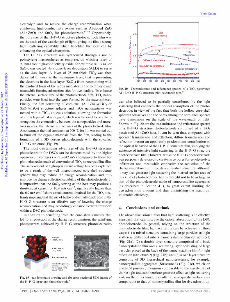
14996 Phys. Chem. Chem. Phys., 2012, 14, 14982–14998 This journal is c the Owner Societies 2012
electrolyte and to reduce the charge recombination when
employing high-conductivity oxides such as Al-doped ZnO
(Al : ZnO) and SnO2 for photoelectrode.64,83 Opportunely,
the pore size of the H–P–G structure photoelectrode film was
on the scale of the wavelength of light, giving the film a strong
light scattering capability which benefited the solar cell by
enhancing the optical absorption.
The H–P–G structure was synthesized through a use of
polystyrene macrospheres as template, on which a layer of
90 nm-thick high-conductivity oxide, for example Al : ZnO or
SnO2, was coated via atomic layer deposition (ALD) to serve
as the host layer. A layer of 25 nm-thick TiO2 was then
deposited to work as the passivation layer, that is preventing
the electrons in the host layer (SnO2) from recombining with
the oxidized form of the redox mediator in the electrolyte and
meanwhile forming adsorption sties for dye loading. To enhance
the internal surface area of the photoelectrode film, TiO2 nano-
particles were filled into the gaps formed by the macrospheres.
Finally, the film consisting of core–shell (Al : ZnO@TiO2 or
SnO2@TiO2) structure spheres and TiO2 nanoparticles was
treated with a TiCl4 aqueous solution, allowing the formation
of a thin layer of TiO2 as guest, which was believed to be able to
strengthen the connectivity between the nanoparticles and more-
over increase the internal surface area of the photoelectrode film.
A consequent thermal treatment at 500 1C for 1 h was carried out
to burn off the organic materials from the film, leading to the
formation of a 3D porous photoelectrode with the so-called
H–P–G structure (Fig. 19).
The most outstanding advantage of the H–P–G structure
photoelectrode for DSCs can be demonstrated by the higher
open-circuit voltages (B791–842 mV) compared to those for
photoelectrodes made of conventional TiO2 nanocrystalline film.
The achievement of high-open circuit voltage has been explained
to be a result of the well interconnected core–shell structure
spheres that may reduce the charge recombination and thus
improve the charge collection capability of the photoelectrode. It
is impressive that the SnO2 serving as the host may produce a
short-circuit current of 10.4 mA cm�2, significantly higher than
the 6.9 mA cm�2 short-circuit current obtained for the TiO2 host,
firmly implying that the use of high-conductivity oxide core in the
H–O–G structure is an effective way of lowering the charge
recombination and may accordingly enhance electron transport
within a DSC photoelectrode.
In addition to benefiting from the core–shell structure that
led to a reduction in the charge recombination, the satisfying
photocurrent achieved by H–P–G structure photoelectrodes
was also believed to be partially contributed by the light
scattering that enhances the optical absorption of the photo-
electrode; in view of the fact that both the hollow core–shell
spheres themselves and the pores among the core–shell spheres
have dimensions on the scale of the wavelength of light.
Shown in Fig. 20 are the transmittance and reflectance spectra
of a H–P–G structure photoelectrode comprised of a TiO2
passivated Al : ZnO host. It can be seen that, compared with
specular transmission and reflection, diffuse transmission and
reflection present an apparently predominant contribution to
the optical behavior of the H–P–G structure film, implying the
existence of intensive light scattering in the H–P–G structure
photoelectrode film. However, while the H–P–G photoelectrode
was purposely developed to create large pores for gel electrolyte
infiltration and meanwhile emphasize the reduction of the
charge recombination through a core–shell structure, although
it may also generate light scattering the internal surface area of
this kind of photoelectrode film is thought not to be as large as
that of the photoelectrode made of nanocrystallite aggregates
(as described in Section 4.1), to great extent limiting the
dye adsorption amount and thus diminishing the maximum
attainable efficiency.
4. Conclusions and outlook
The above discussion attests that light scattering is an effective
approach that can improve the optical absorption of the DSC
photoelectrode. In general, relying on the structure of the
photoelectrode film, light scattering can be achieved in three
ways: (1) a mixed structure containing large particles as light
scatterers embedded into a nanocrystalline film (Structure-1)
(Fig. 21a); (2) a double layer structure comprised of a basic
nanocrystalline film and a scattering layer consisting of large
particles placed at the back of the nanocrystalline film for light
reflection (Structure-2) (Fig. 21b); and (3) a one layer structure
consisting of 3D hierarchical nanostructures, for example,
nanocrystallite aggregates (Structure-3) (Fig. 21c), which on
one hand possess dimensions comparable to the wavelength of
visible light and can therefore generate effective light scattering
and, on the other hand, may offer a large specific surface area
comparable to that of nanocrystalline film for dye adsorption.Fig. 19 (a) Schematic drawing and (b) cross-sectional SEM image of
the H–P–G structure photoelectrode.83
Fig. 20 Transmittance and reflectance spectra of a TiO2-passivated
Al : ZnO H–P–G structure photoelectrode film.84
Dow
nloa
ded
by U
nive
rsity
of
Was
hing
ton
on 2
9 O
ctob
er 2
012
Publ
ishe
d on
05
Sept
embe
r 20
12 o
n ht
tp://
pubs
.rsc
.org
| do
i:10.
1039
/C2C
P430
89D
View Online
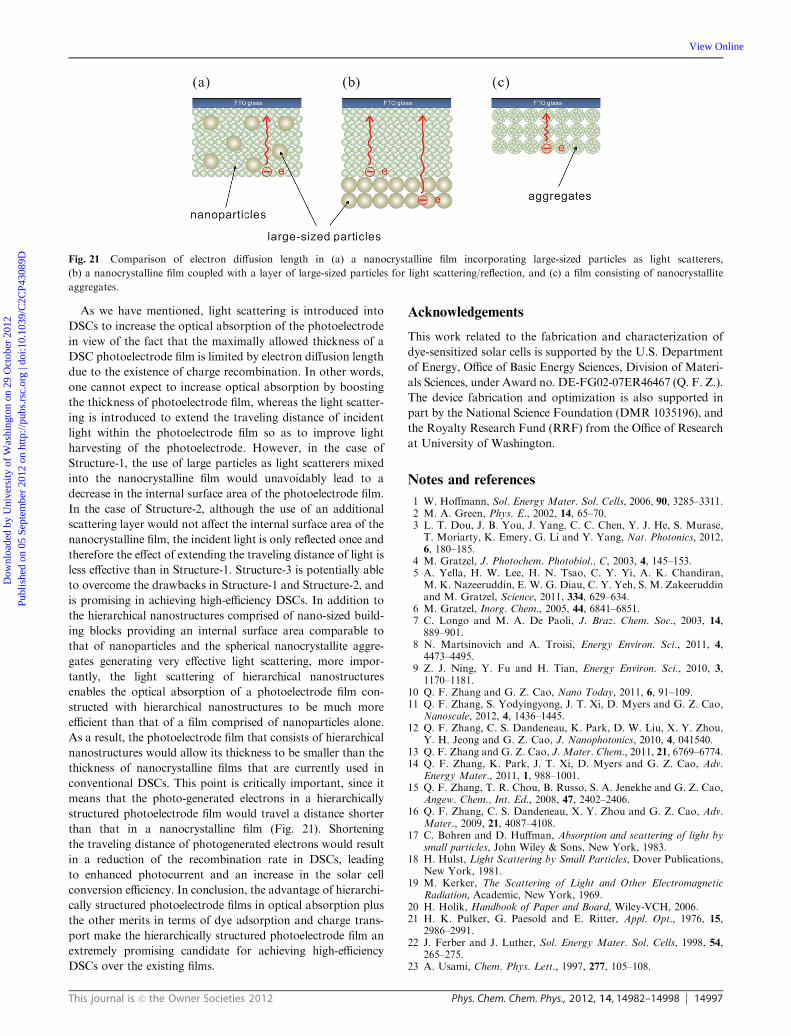
This journal is c the Owner Societies 2012 Phys. Chem. Chem. Phys., 2012, 14, 14982–14998 14997
As we have mentioned, light scattering is introduced into
DSCs to increase the optical absorption of the photoelectrode
in view of the fact that the maximally allowed thickness of a
DSC photoelectrode film is limited by electron diffusion length
due to the existence of charge recombination. In other words,
one cannot expect to increase optical absorption by boosting
the thickness of photoelectrode film, whereas the light scatter-
ing is introduced to extend the traveling distance of incident
light within the photoelectrode film so as to improve light
harvesting of the photoelectrode. However, in the case of
Structure-1, the use of large particles as light scatterers mixed
into the nanocrystalline film would unavoidably lead to a
decrease in the internal surface area of the photoelectrode film.
In the case of Structure-2, although the use of an additional
scattering layer would not affect the internal surface area of the
nanocrystalline film, the incident light is only reflected once and
therefore the effect of extending the traveling distance of light is
less effective than in Structure-1. Structure-3 is potentially able
to overcome the drawbacks in Structure-1 and Structure-2, and
is promising in achieving high-efficiency DSCs. In addition to
the hierarchical nanostructures comprised of nano-sized build-
ing blocks providing an internal surface area comparable to
that of nanoparticles and the spherical nanocrystallite aggre-
gates generating very effective light scattering, more impor-
tantly, the light scattering of hierarchical nanostructures
enables the optical absorption of a photoelectrode film con-
structed with hierarchical nanostructures to be much more
efficient than that of a film comprised of nanoparticles alone.
As a result, the photoelectrode film that consists of hierarchical
nanostructures would allow its thickness to be smaller than the
thickness of nanocrystalline films that are currently used in
conventional DSCs. This point is critically important, since it
means that the photo-generated electrons in a hierarchically
structured photoelectrode film would travel a distance shorter
than that in a nanocrystalline film (Fig. 21). Shortening
the traveling distance of photogenerated electrons would result
in a reduction of the recombination rate in DSCs, leading
to enhanced photocurrent and an increase in the solar cell
conversion efficiency. In conclusion, the advantage of hierarchi-
cally structured photoelectrode films in optical absorption plus
the other merits in terms of dye adsorption and charge trans-
port make the hierarchically structured photoelectrode film an
extremely promising candidate for achieving high-efficiency
DSCs over the existing films.
Acknowledgements
This work related to the fabrication and characterization of
dye-sensitized solar cells is supported by the U.S. Department
of Energy, Office of Basic Energy Sciences, Division of Materi-
als Sciences, under Award no. DE-FG02-07ER46467 (Q. F. Z.).
The device fabrication and optimization is also supported in
part by the National Science Foundation (DMR 1035196), and
the Royalty Research Fund (RRF) from the Office of Research
at University of Washington.
Notes and references
1 W. Hoffmann, Sol. Energy Mater. Sol. Cells, 2006, 90, 3285–3311.2 M. A. Green, Phys. E., 2002, 14, 65–70.3 L. T. Dou, J. B. You, J. Yang, C. C. Chen, Y. J. He, S. Murase,T. Moriarty, K. Emery, G. Li and Y. Yang, Nat. Photonics, 2012,6, 180–185.
4 M. Gratzel, J. Photochem. Photobiol., C, 2003, 4, 145–153.5 A. Yella, H. W. Lee, H. N. Tsao, C. Y. Yi, A. K. Chandiran,M. K. Nazeeruddin, E. W. G. Diau, C. Y. Yeh, S. M. Zakeeruddinand M. Gratzel, Science, 2011, 334, 629–634.
6 M. Gratzel, Inorg. Chem., 2005, 44, 6841–6851.7 C. Longo and M. A. De Paoli, J. Braz. Chem. Soc., 2003, 14,889–901.
8 N. Martsinovich and A. Troisi, Energy Environ. Sci., 2011, 4,4473–4495.
9 Z. J. Ning, Y. Fu and H. Tian, Energy Environ. Sci., 2010, 3,1170–1181.
10 Q. F. Zhang and G. Z. Cao, Nano Today, 2011, 6, 91–109.11 Q. F. Zhang, S. Yodyingyong, J. T. Xi, D. Myers and G. Z. Cao,
Nanoscale, 2012, 4, 1436–1445.12 Q. F. Zhang, C. S. Dandeneau, K. Park, D. W. Liu, X. Y. Zhou,
Y. H. Jeong and G. Z. Cao, J. Nanophotonics, 2010, 4, 041540.13 Q. F. Zhang and G. Z. Cao, J. Mater. Chem., 2011, 21, 6769–6774.14 Q. F. Zhang, K. Park, J. T. Xi, D. Myers and G. Z. Cao, Adv.
Energy Mater., 2011, 1, 988–1001.15 Q. F. Zhang, T. R. Chou, B. Russo, S. A. Jenekhe and G. Z. Cao,
Angew. Chem., Int. Ed., 2008, 47, 2402–2406.16 Q. F. Zhang, C. S. Dandeneau, X. Y. Zhou and G. Z. Cao, Adv.
Mater., 2009, 21, 4087–4108.17 C. Bohren and D. Huffman, Absorption and scattering of light by
small particles, John Wiley & Sons, New York, 1983.18 H. Hulst, Light Scattering by Small Particles, Dover Publications,
New York, 1981.19 M. Kerker, The Scattering of Light and Other Electromagnetic
Radiation, Academic, New York, 1969.20 H. Holik, Handbook of Paper and Board, Wiley-VCH, 2006.21 H. K. Pulker, G. Paesold and E. Ritter, Appl. Opt., 1976, 15,
2986–2991.22 J. Ferber and J. Luther, Sol. Energy Mater. Sol. Cells, 1998, 54,
265–275.23 A. Usami, Chem. Phys. Lett., 1997, 277, 105–108.
Fig. 21 Comparison of electron diffusion length in (a) a nanocrystalline film incorporating large-sized particles as light scatterers,
(b) a nanocrystalline film coupled with a layer of large-sized particles for light scattering/reflection, and (c) a film consisting of nanocrystallite
aggregates.
Dow
nloa
ded
by U
nive
rsity
of
Was
hing
ton
on 2
9 O
ctob
er 2
012
Publ
ishe
d on
05
Sept
embe
r 20
12 o
n ht
tp://
pubs
.rsc
.org
| do
i:10.
1039
/C2C
P430
89D
View Online
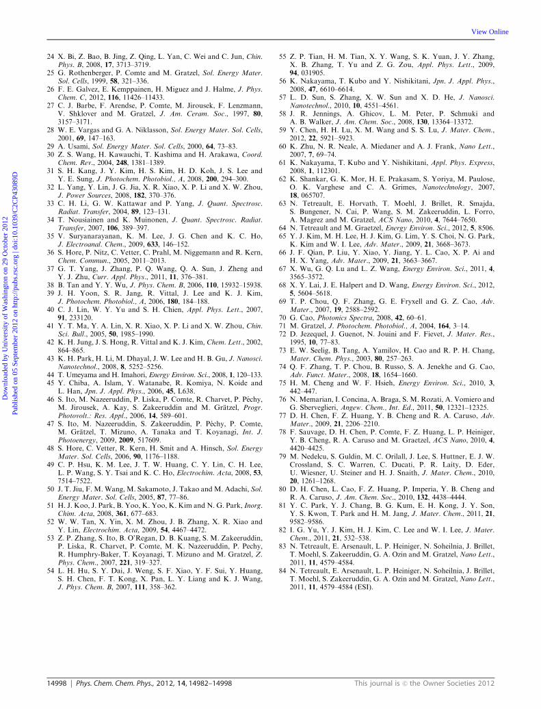
14998 Phys. Chem. Chem. Phys., 2012, 14, 14982–14998 This journal is c the Owner Societies 2012
24 X. Bi, Z. Bao, B. Jing, Z. Qing, L. Yan, C. Wei and C. Jun, Chin.Phys. B, 2008, 17, 3713–3719.
25 G. Rothenberger, P. Comte and M. Gratzel, Sol. Energy Mater.Sol. Cells, 1999, 58, 321–336.
26 F. E. Galvez, E. Kemppainen, H. Miguez and J. Halme, J. Phys.Chem. C, 2012, 116, 11426–11433.
27 C. J. Barbe, F. Arendse, P. Comte, M. Jirousek, F. Lenzmann,V. Shklover and M. Gratzel, J. Am. Ceram. Soc., 1997, 80,3157–3171.
28 W. E. Vargas and G. A. Niklasson, Sol. Energy Mater. Sol. Cells,2001, 69, 147–163.
29 A. Usami, Sol. Energy Mater. Sol. Cells, 2000, 64, 73–83.30 Z. S. Wang, H. Kawauchi, T. Kashima and H. Arakawa, Coord.
Chem. Rev., 2004, 248, 1381–1389.31 S. H. Kang, J. Y. Kim, H. S. Kim, H. D. Koh, J. S. Lee and
Y. E. Sung, J. Photochem. Photobiol., A, 2008, 200, 294–300.32 L. Yang, Y. Lin, J. G. Jia, X. R. Xiao, X. P. Li and X. W. Zhou,
J. Power Sources, 2008, 182, 370–376.33 C. H. Li, G. W. Kattawar and P. Yang, J. Quant. Spectrosc.
Radiat. Transfer, 2004, 89, 123–131.34 T. Nousiainen and K. Muinonen, J. Quant. Spectrosc. Radiat.
Transfer, 2007, 106, 389–397.35 V. Suryanarayanan, K. M. Lee, J. G. Chen and K. C. Ho,
J. Electroanal. Chem., 2009, 633, 146–152.36 S. Hore, P. Nitz, C. Vetter, C. Prahl, M. Niggemann and R. Kern,
Chem. Commun., 2005, 2011–2013.37 G. T. Yang, J. Zhang, P. Q. Wang, Q. A. Sun, J. Zheng and
Y. J. Zhu, Curr. Appl. Phys., 2011, 11, 376–381.38 B. Tan and Y. Y. Wu, J. Phys. Chem. B, 2006, 110, 15932–15938.39 J. H. Yoon, S. R. Jang, R. Vittal, J. Lee and K. J. Kim,
J. Photochem. Photobiol., A, 2006, 180, 184–188.40 C. J. Lin, W. Y. Yu and S. H. Chien, Appl. Phys. Lett., 2007,
91, 233120.41 Y. T. Ma, Y. A. Lin, X. R. Xiao, X. P. Li and X. W. Zhou, Chin.
Sci. Bull., 2005, 50, 1985–1990.42 K. H. Jung, J. S. Hong, R. Vittal and K. J. Kim, Chem. Lett., 2002,
864–865.43 K. H. Park, H. Li, M. Dhayal, J. W. Lee and H. B. Gu, J. Nanosci.
Nanotechnol., 2008, 8, 5252–5256.44 T. Umeyama and H. Imahori, Energy Environ. Sci., 2008, 1, 120–133.45 Y. Chiba, A. Islam, Y. Watanabe, R. Komiya, N. Koide and
L. Han, Jpn. J. Appl. Phys., 2006, 45, L638.46 S. Ito, M. Nazeeruddin, P. Liska, P. Comte, R. Charvet, P. Pechy,
M. Jirousek, A. Kay, S. Zakeeruddin and M. Gratzel, Progr.Photovolt.: Res. Appl., 2006, 14, 589–601.
47 S. Ito, M. Nazeeruddin, S. Zakeeruddin, P. Pechy, P. Comte,M. Gratzel, T. Mizuno, A. Tanaka and T. Koyanagi, Int. J.Photoenergy, 2009, 2009, 517609.
48 S. Hore, C. Vetter, R. Kern, H. Smit and A. Hinsch, Sol. EnergyMater. Sol. Cells, 2006, 90, 1176–1188.
49 C. P. Hsu, K. M. Lee, J. T. W. Huang, C. Y. Lin, C. H. Lee,L. P. Wang, S. Y. Tsai and K. C. Ho, Electrochim. Acta, 2008, 53,7514–7522.
50 J. T. Jiu, F. M. Wang, M. Sakamoto, J. Takao andM. Adachi, Sol.Energy Mater. Sol. Cells, 2005, 87, 77–86.
51 H. J. Koo, J. Park, B. Yoo, K. Yoo, K. Kim and N. G. Park, Inorg.Chim. Acta, 2008, 361, 677–683.
52 W. W. Tan, X. Yin, X. M. Zhou, J. B. Zhang, X. R. Xiao andY. Lin, Electrochim. Acta, 2009, 54, 4467–4472.
53 Z. P. Zhang, S. Ito, B. O’Regan, D. B. Kuang, S. M. Zakeeruddin,P. Liska, R. Charvet, P. Comte, M. K. Nazeeruddin, P. Pechy,R. Humphry-Baker, T. Koyanagi, T. Mizuno and M. Gratzel, Z.Phys. Chem., 2007, 221, 319–327.
54 L. H. Hu, S. Y. Dai, J. Weng, S. F. Xiao, Y. F. Sui, Y. Huang,S. H. Chen, F. T. Kong, X. Pan, L. Y. Liang and K. J. Wang,J. Phys. Chem. B, 2007, 111, 358–362.
55 Z. P. Tian, H. M. Tian, X. Y. Wang, S. K. Yuan, J. Y. Zhang,X. B. Zhang, T. Yu and Z. G. Zou, Appl. Phys. Lett., 2009,94, 031905.
56 K. Nakayama, T. Kubo and Y. Nishikitani, Jpn. J. Appl. Phys.,2008, 47, 6610–6614.
57 L. D. Sun, S. Zhang, X. W. Sun and X. D. He, J. Nanosci.Nanotechnol., 2010, 10, 4551–4561.
58 J. R. Jennings, A. Ghicov, L. M. Peter, P. Schmuki andA. B. Walker, J. Am. Chem. Soc., 2008, 130, 13364–13372.
59 Y. Chen, H. H. Lu, X. M. Wang and S. S. Lu, J. Mater. Chem.,2012, 22, 5921–5923.
60 K. Zhu, N. R. Neale, A. Miedaner and A. J. Frank, Nano Lett.,2007, 7, 69–74.
61 K. Nakayama, T. Kubo and Y. Nishikitani, Appl. Phys. Express,2008, 1, 112301.
62 K. Shankar, G. K. Mor, H. E. Prakasam, S. Yoriya, M. Paulose,O. K. Varghese and C. A. Grimes, Nanotechnology, 2007,18, 065707.
63 N. Tetreault, E. Horvath, T. Moehl, J. Brillet, R. Smajda,S. Bungener, N. Cai, P. Wang, S. M. Zakeeruddin, L. Forro,A. Magrez and M. Gratzel, ACS Nano, 2010, 4, 7644–7650.
64 N. Tetreault and M. Graetzel, Energy Environ. Sci., 2012, 5, 8506.65 Y. J. Kim, M. H. Lee, H. J. Kim, G. Lim, Y. S. Choi, N. G. Park,
K. Kim and W. I. Lee, Adv. Mater., 2009, 21, 3668–3673.66 J. F. Qian, P. Liu, Y. Xiao, Y. Jiang, Y. L. Cao, X. P. Ai and
H. X. Yang, Adv. Mater., 2009, 21, 3663–3667.67 X. Wu, G. Q. Lu and L. Z. Wang, Energy Environ. Sci., 2011, 4,
3565–3572.68 X. Y. Lai, J. E. Halpert and D. Wang, Energy Environ. Sci., 2012,
5, 5604–5618.69 T. P. Chou, Q. F. Zhang, G. E. Fryxell and G. Z. Cao, Adv.
Mater., 2007, 19, 2588–2592.70 G. Cao, Photonics Spectra, 2008, 42, 60–61.71 M. Gratzel, J. Photochem. Photobiol., A, 2004, 164, 3–14.72 D. Jezequel, J. Guenot, N. Jouini and F. Fievet, J. Mater. Res.,
1995, 10, 77–83.73 E. W. Seelig, B. Tang, A. Yamilov, H. Cao and R. P. H. Chang,
Mater. Chem. Phys., 2003, 80, 257–263.74 Q. F. Zhang, T. P. Chou, B. Russo, S. A. Jenekhe and G. Cao,
Adv. Funct. Mater., 2008, 18, 1654–1660.75 H. M. Cheng and W. F. Hsieh, Energy Environ. Sci., 2010, 3,
442–447.76 N. Memarian, I. Concina, A. Braga, S. M. Rozati, A. Vomiero and
G. Sberveglieri, Angew. Chem., Int. Ed., 2011, 50, 12321–12325.77 D. H. Chen, F. Z. Huang, Y. B. Cheng and R. A. Caruso, Adv.
Mater., 2009, 21, 2206–2210.78 F. Sauvage, D. H. Chen, P. Comte, F. Z. Huang, L. P. Heiniger,
Y. B. Cheng, R. A. Caruso and M. Graetzel, ACS Nano, 2010, 4,4420–4425.
79 M. Nedelcu, S. Guldin, M. C. Orilall, J. Lee, S. Huttner, E. J. W.Crossland, S. C. Warren, C. Ducati, P. R. Laity, D. Eder,U. Wiesner, U. Steiner and H. J. Snaith, J. Mater. Chem., 2010,20, 1261–1268.
80 D. H. Chen, L. Cao, F. Z. Huang, P. Imperia, Y. B. Cheng andR. A. Caruso, J. Am. Chem. Soc., 2010, 132, 4438–4444.
81 Y. C. Park, Y. J. Chang, B. G. Kum, E. H. Kong, J. Y. Son,Y. S. Kwon, T. Park and H. M. Jang, J. Mater. Chem., 2011, 21,9582–9586.
82 I. G. Yu, Y. J. Kim, H. J. Kim, C. Lee and W. I. Lee, J. Mater.Chem., 2011, 21, 532–538.
83 N. Tetreault, E. Arsenault, L. P. Heiniger, N. Soheilnia, J. Brillet,T. Moehl, S. Zakeeruddin, G. A. Ozin and M. Gratzel, Nano Lett.,2011, 11, 4579–4584.
84 N. Tetreault, E. Arsenault, L. P. Heiniger, N. Soheilnia, J. Brillet,T. Moehl, S. Zakeeruddin, G. A. Ozin and M. Gratzel, Nano Lett.,2011, 11, 4579–4584 (ESI).
Dow
nloa
ded
by U
nive
rsity
of
Was
hing
ton
on 2
9 O
ctob
er 2
012
Publ
ishe
d on
05
Sept
embe
r 20
12 o
n ht
tp://
pubs
.rsc
.org
| do
i:10.
1039
/C2C
P430
89D
View Online
Related Documents