Carbon nanotubes Chemically Functionalized Carbon Nanotubes Kannan Balasubramanian and Marko Burghard* Artist’s view of carbon nanotubes functionalized with fluorescing particles. From the Contents 1. Introduction............. 181 2. Thermally Activated Chemical Functionalization..... 184 3. Electrochemical Modification of Nanotubes............... 186 4. Photochemical Functionalization of Nanotubes........... 187 5. Applications............. 188 6. Conclusion and Outlook ................................ 191 Keywords: · carbon nanotubes · chemical functionalization · electrochemical modification · photochemistry · sensors 180 # 2005 Wiley-VCH Verlag GmbH & Co. KGaA, D-69451 Weinheim DOI: 10.1002/smll.200400118 small 2005, 1, No. 2, 180 –192 reviews M. Burghard and K. Balasubramanian

Welcome message from author
This document is posted to help you gain knowledge. Please leave a comment to let me know what you think about it! Share it to your friends and learn new things together.
Transcript

Carbon nanotubes
Chemically Functionalized Carbon NanotubesKannan Balasubramanian and Marko Burghard*
Artist’s view of carbon nanotubes functionalized with fluorescing particles.
From the Contents
1. Introduction.............181
2. Thermally ActivatedChemicalFunctionalization.....184
3. ElectrochemicalModification ofNanotubes...............186
4. PhotochemicalFunctionalizationof Nanotubes...........187
5. Applications.............188
6. Conclusion and Outlook................................191
Keywords:· carbon nanotubes· chemical
functionalization· electrochemical
modification· photochemistry· sensors
180 � 2005 Wiley-VCH Verlag GmbH & Co. KGaA, D-69451 Weinheim DOI: 10.1002/smll.200400118 small 2005, 1, No. 2, 180 –192
reviews M. Burghard and K. Balasubramanian
Since their discovery, carbon nanotubes have attracted the attention of manya scientist around the world. This extraordinary interest stems from theiroutstanding structural, mechanical, and electronic properties. In fact, apartfrom being the best and most easily available one-dimensional (1D) modelsystem, carbon nanotubes show strong application potential in electronics,scanning probe microscopy, chemical and biological sensing, reinforcedcomposite materials, and in many more areas. While some of the proposedapplications remain still a far-off dream, others are close to technicalrealization. Recent advances in the development of reliable methods for thechemical functionalization of the nanotubes provide an additional impetustowards extending the scope of their application spectrum. In particular,covalent modification schemes allow persistent alteration of the electronicproperties of the tubes, as well as to chemically tailor their surface properties,whereby new functions can be implemented that cannot otherwise beacquired by pristine nanotubes.
1. Introduction
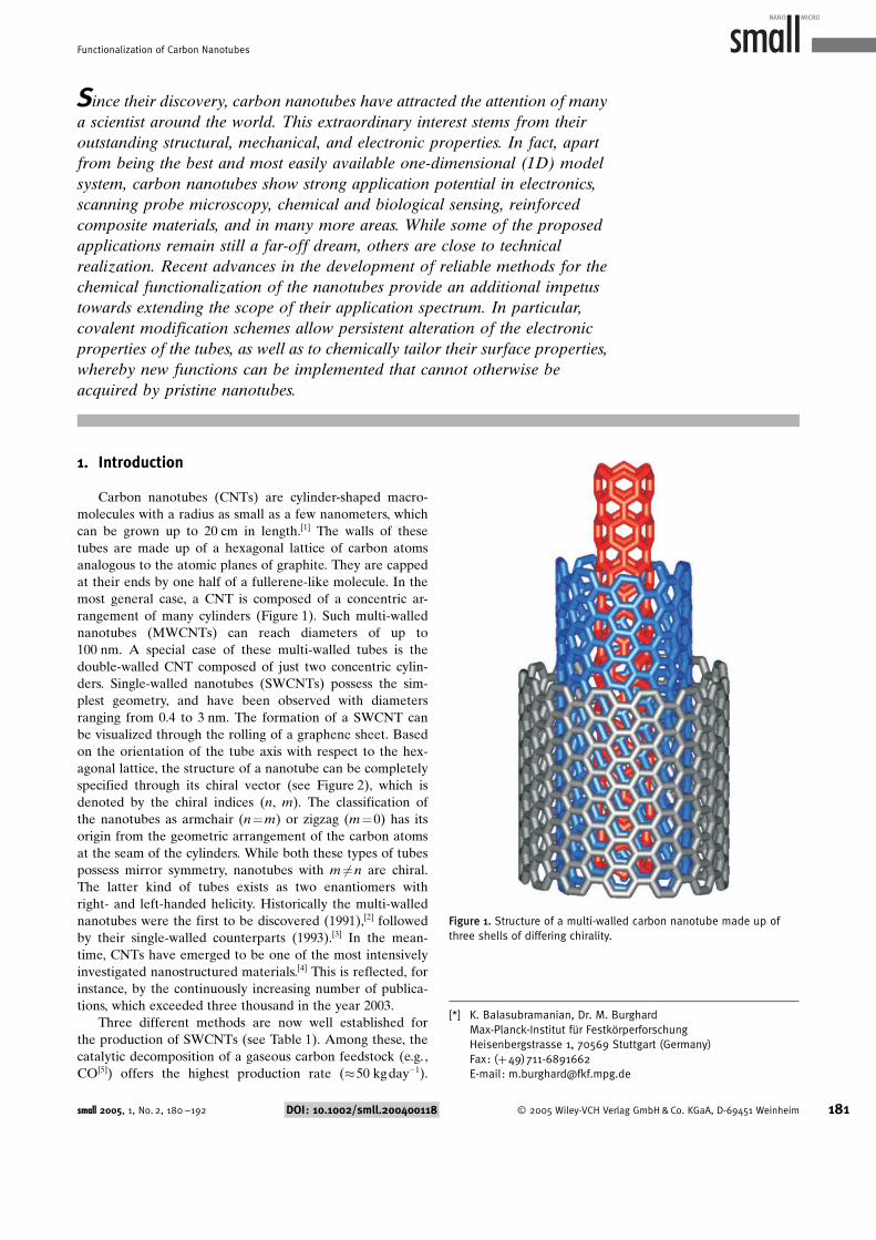
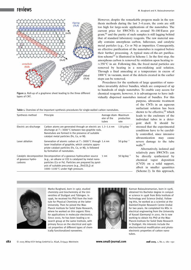
Carbon nanotubes (CNTs) are cylinder-shaped macro-molecules with a radius as small as a few nanometers, whichcan be grown up to 20 cm in length.[1] The walls of thesetubes are made up of a hexagonal lattice of carbon atomsanalogous to the atomic planes of graphite. They are cappedat their ends by one half of a fullerene-like molecule. In themost general case, a CNT is composed of a concentric ar-rangement of many cylinders (Figure 1). Such multi-wallednanotubes (MWCNTs) can reach diameters of up to100 nm. A special case of these multi-walled tubes is thedouble-walled CNT composed of just two concentric cylin-ders. Single-walled nanotubes (SWCNTs) possess the sim-plest geometry, and have been observed with diametersranging from 0.4 to 3 nm. The formation of a SWCNT canbe visualized through the rolling of a graphene sheet. Basedon the orientation of the tube axis with respect to the hex-agonal lattice, the structure of a nanotube can be completelyspecified through its chiral vector (see Figure 2), which isdenoted by the chiral indices (n, m). The classification ofthe nanotubes as armchair (n=m) or zigzag (m=0) has itsorigin from the geometric arrangement of the carbon atomsat the seam of the cylinders. While both these types of tubespossess mirror symmetry, nanotubes with m¼6 n are chiral.The latter kind of tubes exists as two enantiomers withright- and left-handed helicity. Historically the multi-wallednanotubes were the first to be discovered (1991),[2] followedby their single-walled counterparts (1993).[3] In the mean-time, CNTs have emerged to be one of the most intensivelyinvestigated nanostructured materials.[4] This is reflected, forinstance, by the continuously increasing number of publica-tions, which exceeded three thousand in the year 2003.
Three different methods are now well established forthe production of SWCNTs (see Table 1). Among these, thecatalytic decomposition of a gaseous carbon feedstock (e.g.,CO[5]) offers the highest production rate (�50 kgday�1).
[*] K. Balasubramanian, Dr. M. BurghardMax-Planck-Institut f�r FestkçrperforschungHeisenbergstrasse 1, 70569 Stuttgart (Germany)Fax: (+49) 711-6891662E-mail: [email protected]
Figure 1. Structure of a multi-walled carbon nanotube made up ofthree shells of differing chirality.
small 2005, 1, No. 2, 180 –192 DOI: 10.1002/smll.200400118 � 2005 Wiley-VCH Verlag GmbH & Co. KGaA, D-69451 Weinheim 181
Functionalization of Carbon Nanotubes
However, despite the remarkable progress made in the syn-thesis methods during the last 3–4 years, the costs are stilltoo high for large-scale applications of the nanotubes. Thecurrent price for SWCNTs is around 50–100 Euros pergram,[6] and the purity of such samples is still lagging behindthat of standard laboratory reagents. The raw material usu-ally contains amorphous carbon, fullerenes, and catalyticmetal particles (e.g., Co or Ni) as impurities. Consequently,an effective purification of the nanotubes is required beforetheir further processing. A typical state-of-the-art purifica-tion scheme[7] is illustrated in Scheme 1. In the first step, theamorphous carbon is removed by oxidation upon heating to�350 8C in air. Following this, the freed metal particles areremoved by heating in a non-oxidizing acid solution.Through a final annealing at a temperature in excess of1000 8C in vacuum, most of the defects created in the earliersteps can be removed.
Procedures for the synthesis of large quantities of nano-tubes invariably deliver bundles, which are composed of upto hundreds of single nanotubes. To enable easy access forchemical reagents, however, it is advantageous to have indi-vidually dispersed nanotubes instead of bundles. For this
purpose, ultrasonic treatmentof the CNTs in an aqueoussurfactant solution has beenshown to be effective,[8] whichleads to the enclosure of theindividual tubes in a deter-gent shell. It should bestressed that the experimentalconditions have to be careful-ly controlled, since intensiveultrasonication may causesevere damage to the tubewalls.[9]
Alternatively, isolated andrelatively pure SWCNTs canbe directly synthesized bychemical vapor deposition(CVD) on a solid support,albeit in smaller quantities(Scheme 2). In this approach,
Marko Burghard, born in 1967, studiedchemistry and biochemistry at the Uni-versities of Stuttgart and T�bingen. In1996, he received his PhD from the Insti-tute for Physical Chemistry at the latterUniversity. Then he joined the Max-Planck Institute for Solid State Research,where he worked on thin organic filmsfor applications in molecular electronics.Since 2000, he has been leading a re-search group at the same Institute, withprimary focus on the electrical and opti-cal properties of different types of chem-ically functionalized nanowires.
Kannan Balasubramanian, born in 1978,obtained his Bachelor degree in comput-er science in 1998 from Birla Institute ofTechnology and Science (India). Follow-ing this, he worked as a scientist at theDaimlerChrysler Research Centre (India)for two years. He completed his MSc inelectrical engineering from the Universityof Kassel (Germany) in 2001. He is nowworking to obtain his PhD at the Max-Planck-Institute for Solid State Researchin Stuttgart. His interests include theelectrochemical modification and photo-electronic properties of carbon nano-tubes.
Figure 2. Roll-up of a graphene sheet leading to the three differenttypes of CNT.
Table 1. Overview of the important synthesis procedures for single-walled carbon nanotubes.
Synthesis method Principle Average diam-eter of thetubes
Maximumproductionrate
Electric arc-discharge Carbon atoms are generated through an electric arcdischarge at T>3000 8C between two graphite rods.Nanotubes are formed in the presence of suitablecatalyst metal particles (Fe, Co, or Ni).
1.3–1.4 nm 120 g day�1
Laser ablation Generation of atomic carbon at T>3000 8C throughlaser irradiation of graphite, which contains appro-priate catalyst particles (Fe, Co, or Ni), is followedby formation of nanotubes.
1.4 nm 50 g day�1
Catalytic decompositionof gaseous hydro-carbons
Decomposition of a gaseous hydrocarbon source(e.g., an alkane or CO) is catalyzed by metal nano-particles (Co or Fe). Particles are prepared by pyrol-ysis of suitable precursors (e.g., [Fe(CO)5]) at1000–1100 8C under high pressure.
1 nm 50 kg day�1
182 � 2005 Wiley-VCH Verlag GmbH & Co. KGaA, D-69451 Weinheim www.small-journal.com small 2005, 1, No. 2, 180 –192
reviews M. Burghard and K. Balasubramanian
catalyst particles are deposited onto a substrate, and individ-ual SWCNTs with uniform diameters are grown at elevatedtemperatures (>600 8C) from the catalyst particles, using forinstance methane[10] or an alcohol vapor[11] as the carbonsource. An appealing feature of this method is the possibili-ty to control the diameter of the produced tubes throughthe size of the catalyst particles.[12] With the help of litho-graphic techniques, isolated SWCNTs grown in this mannercan then directly be contacted by electrodes, and their elec-trical properties investigated in detail.[13]
Since the emergence of carbon nanotubes, their electri-cal properties have attracted particular interest. Accordingto the zone-folding approach, which derives the electronicstructure of nanotubes directly from graphite, a nanotubebehaves either as a metal or as a semiconductor, dependingon its chiral vector.[14] Within a sample showing no prefer-ence for specific chiralities, one third of the tubes are ex-pected to be metallic, and the remaining two thirds to besemiconducting. Furthermore, the bandgap in semiconduct-ing tubes is predicted to scale inversely with their diameter.Both of these predictions have been verified through numer-ous experimental results.[15] Marked deviations from thezone-folding scheme are encountered only for SWCNTsthat have the smallest diameters (�0.5 nm).[16]
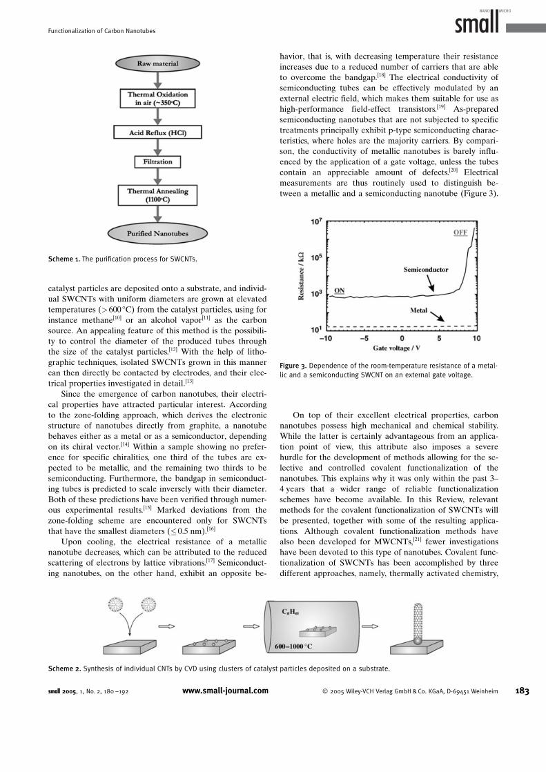
Upon cooling, the electrical resistance of a metallicnanotube decreases, which can be attributed to the reducedscattering of electrons by lattice vibrations.[17] Semiconduct-ing nanotubes, on the other hand, exhibit an opposite be-
havior, that is, with decreasing temperature their resistanceincreases due to a reduced number of carriers that are ableto overcome the bandgap.[18] The electrical conductivity ofsemiconducting tubes can be effectively modulated by anexternal electric field, which makes them suitable for use ashigh-performance field-effect transistors.[19] As-preparedsemiconducting nanotubes that are not subjected to specifictreatments principally exhibit p-type semiconducting charac-teristics, where holes are the majority carriers. By compari-son, the conductivity of metallic nanotubes is barely influ-enced by the application of a gate voltage, unless the tubescontain an appreciable amount of defects.[20] Electricalmeasurements are thus routinely used to distinguish be-tween a metallic and a semiconducting nanotube (Figure 3).
On top of their excellent electrical properties, carbonnanotubes possess high mechanical and chemical stability.While the latter is certainly advantageous from an applica-tion point of view, this attribute also imposes a severehurdle for the development of methods allowing for the se-lective and controlled covalent functionalization of thenanotubes. This explains why it was only within the past 3–4 years that a wider range of reliable functionalizationschemes have become available. In this Review, relevantmethods for the covalent functionalization of SWCNTs willbe presented, together with some of the resulting applica-tions. Although covalent functionalization methods havealso been developed for MWCNTs,[21] fewer investigationshave been devoted to this type of nanotubes. Covalent func-tionalization of SWCNTs has been accomplished by threedifferent approaches, namely, thermally activated chemistry,
Scheme 1. The purification process for SWCNTs.
Scheme 2. Synthesis of individual CNTs by CVD using clusters of catalyst particles deposited on a substrate.
Figure 3. Dependence of the room-temperature resistance of a metal-lic and a semiconducting SWCNT on an external gate voltage.
small 2005, 1, No. 2, 180 –192 www.small-journal.com � 2005 Wiley-VCH Verlag GmbH & Co. KGaA, D-69451 Weinheim 183
Functionalization of Carbon Nanotubes
electrochemical modification, and photochemical functional-ization.
Ideal SWCNTs possess two distinct regions of differingreactivity towards covalent chemical modification. The pres-ence of five-membered rings at the caps leads to a relativelyhigher reactivity at these points, comparable to the reactivi-ty of fullerenes.[22] By comparison, functionalization of thesidewall comprising the regular graphene framework ismore difficult to accomplish. In general, addition reactionsto the partial carbon–carbon double bonds cause the trans-formation of sp2- into sp3-hybridized carbon atoms, which isassociated with a change from a trigonal-planar local bond-ing geometry to a tetrahedral geometry. This process is ener-getically more favorable at the caps due to their pronouncedcurvature in two dimensions, in marked contrast to the side-wall with its comparatively low curvature in only one di-mension. On the other hand, the non-zero curvature makesthe sidewall more reactive than a planar graphene sheet.Correspondingly, the binding energy of atoms or functionalgroups on the sidewall should increase with decreasing tubediameter. This tendency is supported by theoretical studies,as has been reported, for instance, for the bonding of alkylradicals to the sidewall of a SWCNT.[23] On the contrary, theconcave curvature of the inner surface of the nanotube im-parts a very low reactivity towards addition reactions,[24] sothat carbon nanotubes have been proposed as nano-contain-ers for reactive gas atoms, analogous to fullerenes encapsu-lating nitrogen atoms (e.g., N@C60).
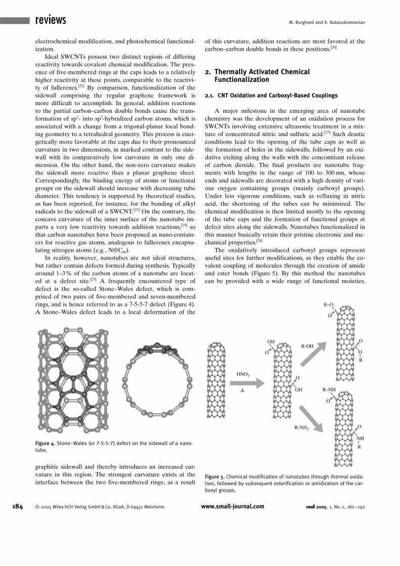
In reality, however, nanotubes are not ideal structures,but rather contain defects formed during synthesis. Typicallyaround 1–3% of the carbon atoms of a nanotube are locat-ed at a defect site.[25] A frequently encountered type ofdefect is the so-called Stone–Wales defect, which is com-prised of two pairs of five-membered and seven-memberedrings, and is hence referred to as a 7-5-5-7 defect (Figure 4).A Stone–Wales defect leads to a local deformation of the
graphitic sidewall and thereby introduces an increased cur-vature in this region. The strongest curvature exists at theinterface between the two five-membered rings; as a result
of this curvature, addition reactions are most favored at thecarbon–carbon double bonds in these positions.[26]
2. Thermally Activated ChemicalFunctionalization
2.1. CNT Oxidation and Carboxyl-Based Couplings
A major milestone in the emerging area of nanotubechemistry was the development of an oxidation process forSWCNTs involving extensive ultrasonic treatment in a mix-ture of concentrated nitric and sulfuric acid.[27] Such drasticconditions lead to the opening of the tube caps as well asthe formation of holes in the sidewalls, followed by an oxi-dative etching along the walls with the concomitant releaseof carbon dioxide. The final products are nanotube frag-ments with lengths in the range of 100 to 300 nm, whoseends and sidewalls are decorated with a high density of vari-ous oxygen containing groups (mainly carboxyl groups).Under less vigorous conditions, such as refluxing in nitricacid, the shortening of the tubes can be minimized. Thechemical modification is then limited mostly to the openingof the tube caps and the formation of functional groups atdefect sites along the sidewalls. Nanotubes functionalized inthis manner basically retain their pristine electronic and me-chanical properties.[28]
The oxidatively introduced carboxyl groups representuseful sites for further modifications, as they enable the co-valent coupling of molecules through the creation of amideand ester bonds (Figure 5). By this method the nanotubescan be provided with a wide range of functional moieties,
Figure 4. Stone–Wales (or 7-5-5-7) defect on the sidewall of a nano-tube.
Figure 5. Chemical modification of nanotubes through thermal oxida-tion, followed by subsequent esterification or amidization of the car-boxyl groups.
184 � 2005 Wiley-VCH Verlag GmbH & Co. KGaA, D-69451 Weinheim www.small-journal.com small 2005, 1, No. 2, 180 –192
reviews M. Burghard and K. Balasubramanian
for which purpose bifunctional molecules (e.g., diamines)are often utilized as linkers. Illustrative examples are nano-tubes equipped with dendrimers, nucleic acids, enzymes,metal complexes, or semiconductor and metal nanoparti-cles.[29] Another interesting application of the carboxylgroups is the formation of an anhydride at the tube ends,through which rings of nanotubes are accessible.[30]
The presence of (modified) carboxyl groups leads to areduction of van der Waals interactions between the CNTs,which strongly facilitates the separation of nanotube bun-dles into individual tubes. Additionally, the attachment ofsuitable groups renders the tubes soluble in aqueous or or-ganic solvents, opening the possibility of further modifica-tions through subsequent solution-based chemistry. A highwater solubility of a few tenths of a gram per milliliter hasrecently been achieved on the basis of the carboxyl-basedcoupling of hydrophilic polymers such as poly(ethyleneglycol) (PEG).[31] SWCNTs with a good solubility in organicsolvents can be obtained by covalent[32] or ionic[33] attach-ment of long-chain aliphatic amines onto the carboxylgroups.
2.2. Addition Reactions at the Sidewall
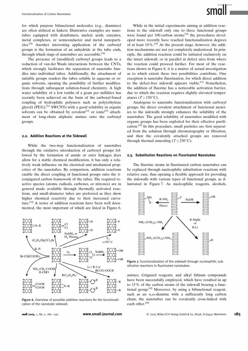
While the two-step functionalization of nanotubesthrough the oxidative introduction of carboxyl groups fol-lowed by the formation of amide or ester linkages doesallow for a stable chemical modification, it has only a rela-tively weak influence on the electrical and mechanical prop-erties of the nanotubes. By comparison, addition reactionsenable the direct coupling of functional groups onto the p-conjugated carbon framework of the tubes. The required re-active species (atoms, radicals, carbenes, or nitrenes) are ingeneral made available through thermally activated reac-tions, and small-diameter tubes are preferred as they showhigher chemical reactivity due to their increased curva-ture.[34] A series of addition reactions have been well docu-mented, the most important of which are listed in Figure 6.
While in the initial experiments aiming at addition reac-tions to the sidewall only one to three functional groupswere found per 100 carbon atoms,[35] the procedures devel-oped more recently have reached functionalization degreesof at least 10 %.[36] At the present stage, however, the addi-tion mechanisms are not yet completely understood. In prin-ciple, the addition reaction could be initiated exclusively onthe intact sidewall, or in parallel at defect sites from wherethe reaction could proceed further. For most of the reac-tions shown in Figure 8, it is a matter of actual investigationas to which extent these two possibilities contribute. Oneexception is nanotube fluorination, for which direct additionto the defect-free sidewall appears viable.[37] Nonetheless,the addition of fluorine has a noticeable activation barrier,due to which the reaction requires slightly elevated temper-atures (T>150 8C).
Analogous to nanotube functionalization with carboxylgroups, the direct covalent attachment of functional moiet-ies to the sidewalls strongly enhances the solubility of thenanotubes. The good solubility of nanotubes modified withorganic groups has been exploited for their effective purifi-cation.[38] In this procedure, small particles are first separat-ed from the solution through chromatography or filtration,and then the covalently attached groups are removedthrough thermal annealing (T>250 8C).
2.3. Substitution Reactions on Fluorinated Nanotubes
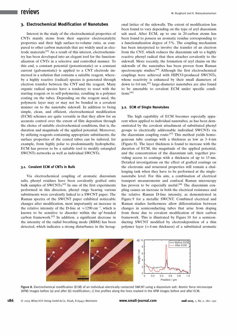
The fluorine atoms in fluorinated carbon nanotubes canbe replaced through nucleophilic substitution reactions withrelative ease, thus opening a flexible approach for providingthe sidewalls with various types of functional groups, as il-lustrated in Figure 7. As nucleophilic reagents, alcohols,
amines, Grignard reagents, and alkyl lithium compoundshave been successfully employed, which have resulted in upto 15% of the carbon atoms of the sidewall bearing a func-tional group.[39] Moreover, by using a bifunctional reagent,such as an a,w-diamine with a sufficiently long carbonchain, the nanotubes can be covalently cross-linked witheach other.[40]
Figure 6. Overview of possible addition reactions for the functionali-zation of the nanotube sidewall.
Figure 7. Functionalization of the sidewall through nucleophilic sub-stitution reactions in fluorinated nanotubes.
small 2005, 1, No. 2, 180 –192 www.small-journal.com � 2005 Wiley-VCH Verlag GmbH & Co. KGaA, D-69451 Weinheim 185
Functionalization of Carbon Nanotubes
3. Electrochemical Modification of Nanotubes
Interest in the study of the electrochemical properties ofCNTs mainly stems from their superior electrocatalyticproperties and their high surface-to-volume ratio, as com-pared to other carbon materials that are widely used as elec-trode materials.[41] As a result of this interest, electrochemis-try has been developed into an elegant tool for the function-alization of CNTs in a selective and controlled manner. Tothis end, a constant potential (potentiostatic) or a constantcurrent (galvanostatic) is applied to a CNT electrode im-mersed in a solution that contains a suitable reagent, where-by a highly reactive (radical) species is generated throughelectron transfer between the CNT and the reagent. Manyorganic radical species have a tendency to react with thestarting reagent or to self-polymerize, resulting in a polymercoating on the tubes. Depending on the reagent used, thepolymeric layer may or may not be bonded in a covalentmanner on to the nanotube sidewall. In addition to beingsimple, clean, and efficient, electrochemical modification(ECM) schemes are quite versatile in that they allow for anaccurate control over the extent of film deposition throughthe choice of suitable electrochemical conditions, that is, theduration and magnitude of the applied potential. Moreover,by utilizing reagents containing appropriate substituents, thesurface properties of the coated tubes can be tailored, forexample, from highly polar to predominantly hydrophobic.ECM has proven to be a suitable tool to modify entangledSWCNTs networks as well as individual SWCNTs.
3.1. Covalent ECM of CNTs in Bulk
Via electrochemical coupling of aromatic diazoniumsalts, phenyl residues have been covalently grafted ontobulk samples of SWCNTs.[42] In one of the first experimentsperformed in this direction, phenyl rings bearing varioussubstituents were covalently linked to a SWCNT paper. TheRaman spectra of the SWCNT paper exhibited noticeablechanges after modification, most importantly an increase inthe relative intensity of the D-line at �1290 cm�1, which isknown to be sensitive to disorder within the sp2-bondedcarbon framework.[43] In addition, a significant decrease inthe intensity of the radial breathing mode (RBM) has beendetected, which indicates a strong disturbance in the hexag-
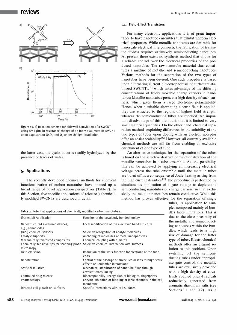
onal lattice of the sidewalls. The extent of modification hasbeen found to vary depending on the type of aryl diazoniumsalt used. After ECM, up to one in 20 carbon atoms hasbeen found to possess an aromatic residue corresponding toa functionalization degree of 5%. The coupling mechanismhas been interpreted to involve the transfer of an electronfrom the CNT, which reduces the diazonium salt to a highlyreactive phenyl radical that then attaches covalently to thesidewall. More recently, the formation of aryl chains on thesidewalls of the nanotubes has been proven from Ramanspectroscopic studies.[44] Although the first electrochemicalcouplings were achieved with HIPCO-produced SWCNTs,whose reactivity is enhanced by their small diameters ofdown to 0.6 nm,[45] large-diameter nanotubes are also foundto be amenable to covalent ECM under specific condi-tions.[46]
3.2. ECM of Single Nanotubes
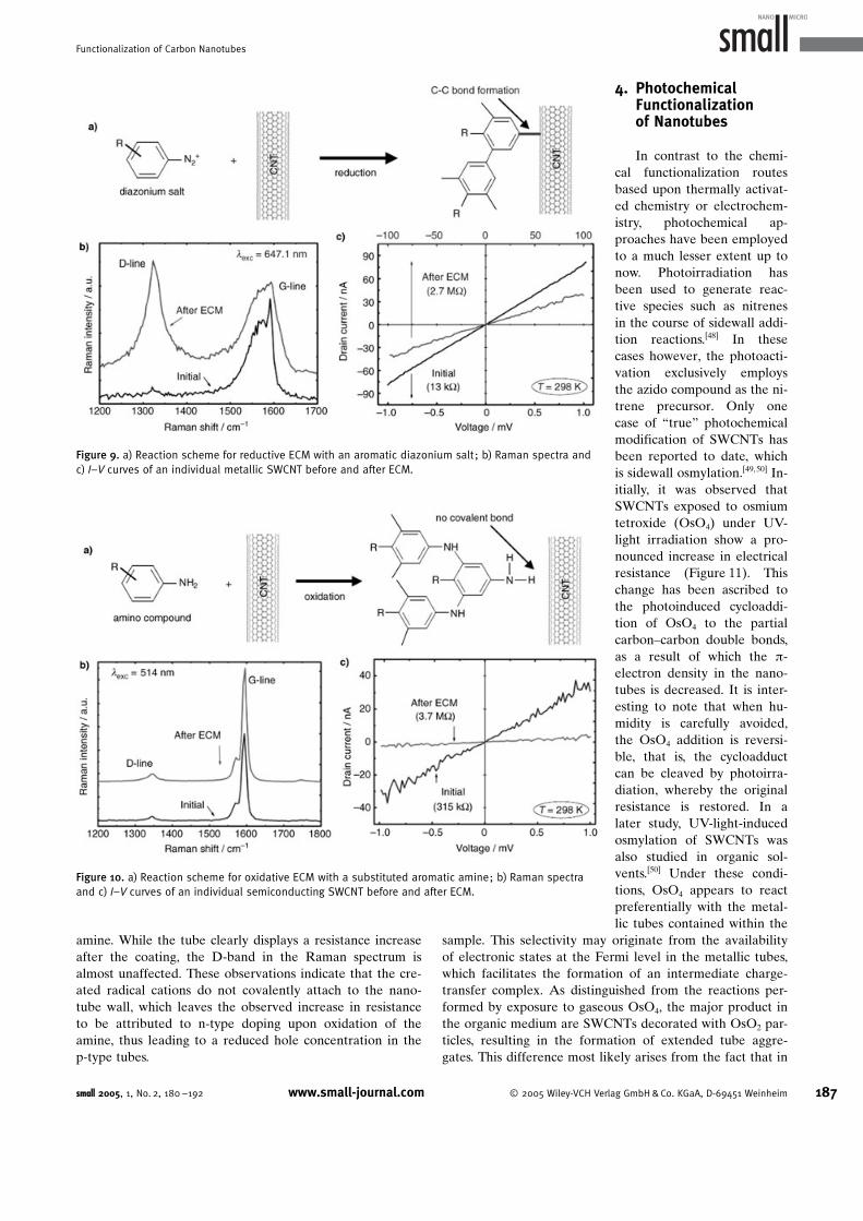
The high capability of ECM becomes especially appa-rent when applied to individual nanotubes, as has been dem-onstrated by the covalent attachment of substituted phenylgroups to electrically addressable individual SWCNTs viathe diazonium coupling route.[47] This method yields homo-geneous tube coatings with a thickness as low as 3–4 nm(Figure 8). The layer thickness is found to increase with theduration of ECM, the magnitude of the applied potential,and the concentration of the diazonium salt, together pro-viding access to coatings with a thickness of up to 15 nm.Detailed investigations on the effect of grafted coatings onthe electronic and structural properties still remain a chal-lenging task when they have to be performed at the single-nanotube level. For this aim, a combination of electricaltransport measurements and confocal Raman microscopyhas proven to be especially useful.[46] The diazonium cou-pling causes an increase in both the electrical resistance andthe relative Raman D-line intensity, as demonstrated inFigure 9 for a metallic SWCNT. Combined electrical andRaman studies furthermore allow differentiation betweenchanges in semiconducting tubes that arise from dopingfrom those due to covalent modification of their carbonframework. This is illustrated by Figure 10 for a semicon-ducting SWCNT modified by electrodeposition of a thinpolymer layer (�4 nm thickness) of a substituted aromatic
Figure 8. Electrochemical modification (ECM) of an individual electrically contacted SWCNT using a diazonium salt: Atomic force microscope(AFM) images before (a) and after (b) modification; c) line profiles along the lines marked in the AFM images before and after ECM.
186 � 2005 Wiley-VCH Verlag GmbH & Co. KGaA, D-69451 Weinheim www.small-journal.com small 2005, 1, No. 2, 180 –192
reviews M. Burghard and K. Balasubramanian
amine. While the tube clearly displays a resistance increaseafter the coating, the D-band in the Raman spectrum isalmost unaffected. These observations indicate that the cre-ated radical cations do not covalently attach to the nano-tube wall, which leaves the observed increase in resistanceto be attributed to n-type doping upon oxidation of theamine, thus leading to a reduced hole concentration in thep-type tubes.
4. PhotochemicalFunctionalizationof Nanotubes
In contrast to the chemi-cal functionalization routesbased upon thermally activat-ed chemistry or electrochem-istry, photochemical ap-proaches have been employedto a much lesser extent up tonow. Photoirradiation hasbeen used to generate reac-tive species such as nitrenesin the course of sidewall addi-tion reactions.[48] In thesecases however, the photoacti-vation exclusively employsthe azido compound as the ni-trene precursor. Only onecase of “true” photochemicalmodification of SWCNTs hasbeen reported to date, whichis sidewall osmylation.[49,50] In-itially, it was observed thatSWCNTs exposed to osmiumtetroxide (OsO4) under UV-light irradiation show a pro-nounced increase in electricalresistance (Figure 11). Thischange has been ascribed tothe photoinduced cycloaddi-tion of OsO4 to the partialcarbon–carbon double bonds,as a result of which the p-electron density in the nano-tubes is decreased. It is inter-esting to note that when hu-midity is carefully avoided,the OsO4 addition is reversi-ble, that is, the cycloadductcan be cleaved by photoirra-diation, whereby the originalresistance is restored. In alater study, UV-light-inducedosmylation of SWCNTs wasalso studied in organic sol-vents.[50] Under these condi-tions, OsO4 appears to reactpreferentially with the metal-lic tubes contained within the
sample. This selectivity may originate from the availabilityof electronic states at the Fermi level in the metallic tubes,which facilitates the formation of an intermediate charge-transfer complex. As distinguished from the reactions per-formed by exposure to gaseous OsO4, the major product inthe organic medium are SWCNTs decorated with OsO2 par-ticles, resulting in the formation of extended tube aggre-gates. This difference most likely arises from the fact that in
Figure 9. a) Reaction scheme for reductive ECM with an aromatic diazonium salt; b) Raman spectra andc) I–V curves of an individual metallic SWCNT before and after ECM.
Figure 10. a) Reaction scheme for oxidative ECM with a substituted aromatic amine; b) Raman spectraand c) I–V curves of an individual semiconducting SWCNT before and after ECM.
small 2005, 1, No. 2, 180 –192 www.small-journal.com � 2005 Wiley-VCH Verlag GmbH & Co. KGaA, D-69451 Weinheim 187
Functionalization of Carbon Nanotubes
the latter case, the cycloadduct is readily hydrolyzed by thepresence of traces of water.
5. Applications
The recently developed chemical methods for chemicalfunctionalization of carbon nanotubes have opened up abroad range of novel application perspectives (Table 2). Inthis Section, five specific applications of (electro-) chemical-ly modified SWCNTs are described in detail.
5.1. Field-Effect Transistors
For many electronic applications it is of great impor-tance to have nanotube ensembles that exhibit uniform elec-trical properties. While metallic nanotubes are desirable fornanoscale electrical interconnects, the fabrication of transis-tor devices requires exclusively semiconducting nanotubes.At present there exists no synthesis method that allows fora reliable control over the electrical properties of the pro-duced nanotubes. The raw nanotube material thus consti-tutes a mixture of metallic and semiconducting nanotubes.Various methods for the separation of the two types ofnanotubes have been devised. One such procedure is basedupon alternating current dielectrophoresis of surfactant-sta-bilized SWCNTs,[51] which takes advantage of the differingconcentrations of freely movable charge carriers in nano-tubes: Metallic nanotubes possess a high density of such car-riers, which gives them a large electronic polarizability.Hence, when a suitable alternating electric field is applied,they are attracted to the regions of highest field strength,whereas the semiconducting tubes are repelled. An impor-tant disadvantage of this method is that it is limited to verysmall material quantities. On the other hand, chemical sepa-ration methods exploiting differences in the solubility of thetwo types of tubes upon doping with an electron acceptoroffer an easier scalability.[52] However, all currently availablechemical methods are still far from enabling an exclusiveenrichment of one type of tube.
An alternative technique for the separation of the tubesis based on the selective destruction/functionalization of themetallic nanotubes in a tube ensemble. As one possibility,this can be achieved by applying an increasing electricalvoltage across the tube ensemble until the metallic tubesare burnt off as a consequence of Joule heating arising fromthe high current densities.[53] The procedure is performed bysimultaneous application of a gate voltage to deplete thesemiconducting nanotubes of charge carriers, so that exclu-sively the metallic nanotubes remain conductive. While thismethod has proven effective for the separation of single
tubes, its application to sam-ples composed mainly of bun-dles faces limitations. This isdue to the close proximity ofthe metallic and semiconduct-ing nanotubes within the bun-dles, which leads to a highrisk of damage for the lattertype of tubes. Electrochemicalmethods offer an elegant so-lution to this problem. Uponswitching off the semicon-ducting tubes under appropri-ate gate control, the metallictubes are exclusively providedwith a high density of cova-lently coupled phenyl radicalsreductively generated fromaromatic diazonium salts (seeSections 3.1 and 3.2). As a
Figure 11. a) Reaction scheme for sidewall osmylation of a SWCNTusing UV light; b) resistance change of an individual metallic SWCNTupon exposure to OsO4 and O2 under UV-light irradiation.
Table 2. Potential applications of chemically modified carbon nanotubes.
(Potential) Application Function of the covalently bonded moiety
Nanostructured electronic devices,e.g., nanodiodes
Local modification of the electronic band structure
(Bio-) chemical sensors Selective recognition of analyte moleculesCatalyst supports Anchoring of molecules or metal nanoparticlesMechanically reinforced composites Chemical coupling with a matrixChemically sensitive tips for scanning probemicroscopy
Selective chemical interaction with surfaces
Field emission Reduction of the work function for electrons at the tubeends
Nanofiltration Control of the passage of molecules or ions through stericeffects or Coulombic interactions
Artificial muscles Mechanical stabilization of nanotube films throughcovalent cross-linking
Controlled drug release Biocompatibility; recognition of biological fingerprintsPharmacology Enzyme inhibition or blocking of ionic channels in the cell
membraneDirected cell growth on surfaces Specific interactions with cell surfaces
188 � 2005 Wiley-VCH Verlag GmbH & Co. KGaA, D-69451 Weinheim www.small-journal.com small 2005, 1, No. 2, 180 –192
reviews M. Burghard and K. Balasubramanian
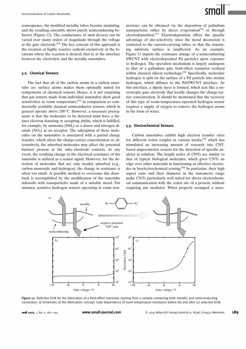
consequence, the modified metallic tubes become insulating,and the resulting ensemble shows purely semiconducting be-havior (Figure 12). The conductance of such devices can bevaried over many orders of magnitude through the voltageat the gate electrode.[54] The key concept of this approach isthe creation of highly reactive radicals exclusively at the lo-cations where the reaction is desired, that is, at the interfacebetween the electrolyte and the metallic nanotubes.
5.2. Chemical Sensors
The fact that all of the carbon atoms in a carbon nano-tube are surface atoms makes them optimally suited forcomponents of chemical sensors. Hence, it is not surprisingthat gas sensors made from individual nanotubes show goodsensitivities at room temperature,[55] in comparison to com-mercially available classical semiconductor sensors, which ingeneral operate above 200 8C. However, a necessary prereq-uisite is that the molecules to be detected must have a dis-tinct electron donating or accepting ability, which is fulfilled,for example, by ammonia (NH3) as a donor and nitrogen di-oxide (NO2) as an acceptor. The adsorption of these mole-cules on the nanotubes is associated with a partial chargetransfer, which alters the charge-carrier concentration or, al-ternatively, the adsorbed molecules may affect the potentialbarriers present at the tube–electrode contacts. In anyevent, the resulting change in the electrical resistance of thenanotube is utilized as a sensor signal. However, for the de-tection of molecules that are only weakly adsorbed (e.g.,carbon monoxide and hydrogen), the change in resistance isoften too small. A possible method to overcome this draw-back is accomplished by the modification of the nanotubesidewalls with nanoparticles made of a suitable metal. Forinstance, sensitive hydrogen sensors operating at room tem-
perature can be obtained via the deposition of palladiumnanoparticles either by direct evaporation[56] or throughelectrodeposition.[57] Electrodeposition offers the specificadvantage of site-selectivity, since the metal decoration isrestricted to the current-carrying tubes, so that the remain-ing substrate surface is unaffected. As an example,Figure 13 depicts the resistance change of a semiconductingSWCNT with electrodeposited Pd particles upon exposureto hydrogen. The operation mechanism is largely analogousto that of a palladium gate field-effect transistor realizedwithin classical silicon technology.[58] Specifically, molecularhydrogen is split on the surface of a Pd particle into atomichydrogen, which diffuses to the Pd/SWCNT interface. Atthis interface, a dipole layer is formed, which acts like a mi-croscopic gate electrode that locally changes the charge-car-rier concentration. It should be mentioned that the recoveryof this type of room-temperature-operated hydrogen sensorrequires a supply of oxygen to remove the hydrogen atomsin the form of water.
5.3. Electrochemical Sensors
Carbon nanotubes exhibit high electron transfer ratesfor different redox couples in various media,[59] which hasstimulated an increasing amount of research into CNT-based amperometric sensors for the detection of specific an-alytes in solution. The length scales of CNTs are similar tothat of typical biological molecules, which gives CNTs anedge over other materials in functioning as effective electro-des in bioelectrochemical sensing.[60] In particular, their highaspect ratio and their diameter in the nanometer rangemake CNTs particularly well suited for direct electrochemi-cal communication with the redox site of a protein, withoutrequiring any mediator. When properly arranged, a nano-
Figure 12. Selective ECM for the fabrication of a field-effect transistor starting from a sample containing both metallic and semiconductingnanotubes: a) Schematic of the fabrication concept. Gate dependence of room-temperature resistance before (b) and after (c) selective ECM.
small 2005, 1, No. 2, 180 –192 www.small-journal.com � 2005 Wiley-VCH Verlag GmbH & Co. KGaA, D-69451 Weinheim 189
Functionalization of Carbon Nanotubes
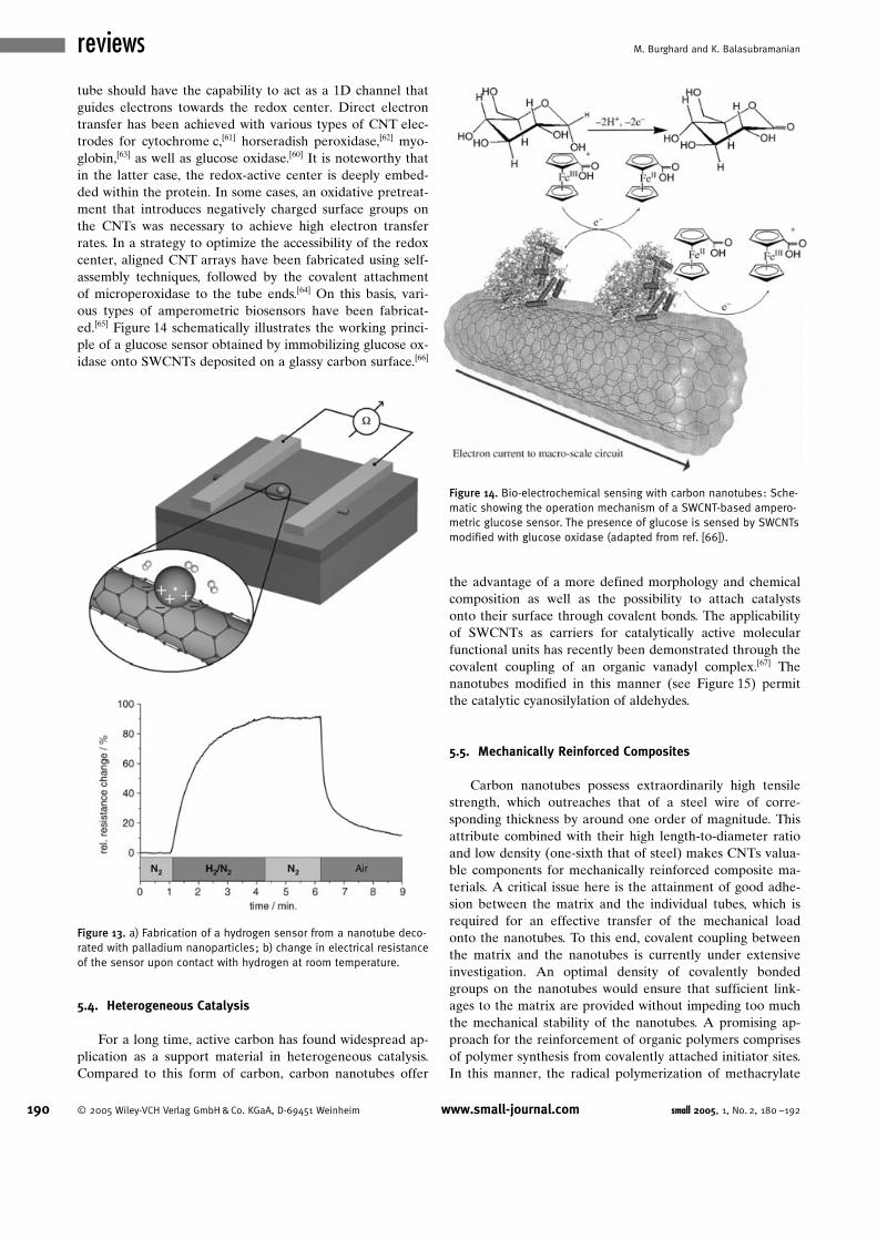
tube should have the capability to act as a 1D channel thatguides electrons towards the redox center. Direct electrontransfer has been achieved with various types of CNT elec-trodes for cytochrome c,[61] horseradish peroxidase,[62] myo-globin,[63] as well as glucose oxidase.[60] It is noteworthy thatin the latter case, the redox-active center is deeply embed-ded within the protein. In some cases, an oxidative pretreat-ment that introduces negatively charged surface groups onthe CNTs was necessary to achieve high electron transferrates. In a strategy to optimize the accessibility of the redoxcenter, aligned CNT arrays have been fabricated using self-assembly techniques, followed by the covalent attachmentof microperoxidase to the tube ends.[64] On this basis, vari-ous types of amperometric biosensors have been fabricat-ed.[65] Figure 14 schematically illustrates the working princi-ple of a glucose sensor obtained by immobilizing glucose ox-idase onto SWCNTs deposited on a glassy carbon surface.[66]
5.4. Heterogeneous Catalysis
For a long time, active carbon has found widespread ap-plication as a support material in heterogeneous catalysis.Compared to this form of carbon, carbon nanotubes offer
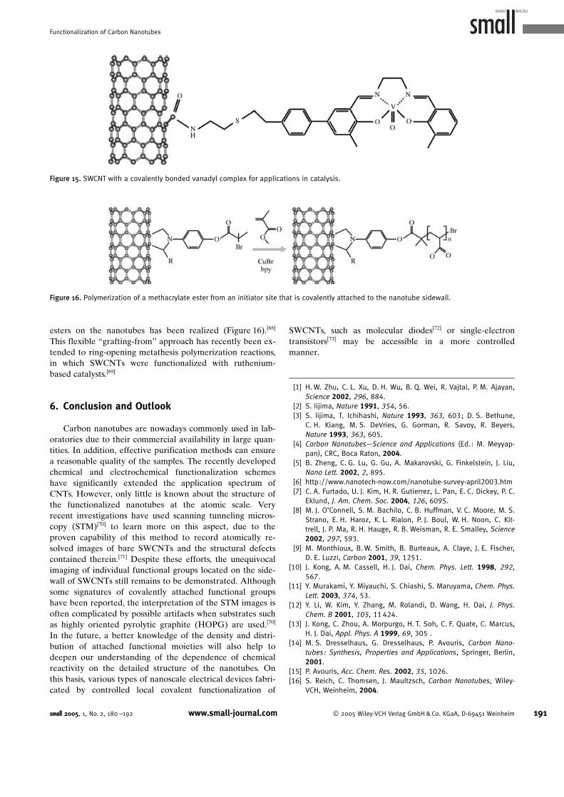
the advantage of a more defined morphology and chemicalcomposition as well as the possibility to attach catalystsonto their surface through covalent bonds. The applicabilityof SWCNTs as carriers for catalytically active molecularfunctional units has recently been demonstrated through thecovalent coupling of an organic vanadyl complex.[67] Thenanotubes modified in this manner (see Figure 15) permitthe catalytic cyanosilylation of aldehydes.
5.5. Mechanically Reinforced Composites
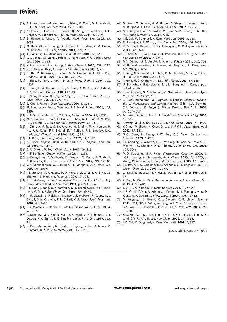
Carbon nanotubes possess extraordinarily high tensilestrength, which outreaches that of a steel wire of corre-sponding thickness by around one order of magnitude. Thisattribute combined with their high length-to-diameter ratioand low density (one-sixth that of steel) makes CNTs valua-ble components for mechanically reinforced composite ma-terials. A critical issue here is the attainment of good adhe-sion between the matrix and the individual tubes, which isrequired for an effective transfer of the mechanical loadonto the nanotubes. To this end, covalent coupling betweenthe matrix and the nanotubes is currently under extensiveinvestigation. An optimal density of covalently bondedgroups on the nanotubes would ensure that sufficient link-ages to the matrix are provided without impeding too muchthe mechanical stability of the nanotubes. A promising ap-proach for the reinforcement of organic polymers comprisesof polymer synthesis from covalently attached initiator sites.In this manner, the radical polymerization of methacrylate
Figure 13. a) Fabrication of a hydrogen sensor from a nanotube deco-rated with palladium nanoparticles; b) change in electrical resistanceof the sensor upon contact with hydrogen at room temperature.
Figure 14. Bio-electrochemical sensing with carbon nanotubes: Sche-matic showing the operation mechanism of a SWCNT-based ampero-metric glucose sensor. The presence of glucose is sensed by SWCNTsmodified with glucose oxidase (adapted from ref. [66]).
190 � 2005 Wiley-VCH Verlag GmbH & Co. KGaA, D-69451 Weinheim www.small-journal.com small 2005, 1, No. 2, 180 –192
reviews M. Burghard and K. Balasubramanian
esters on the nanotubes has been realized (Figure 16).[68]
This flexible “grafting-from” approach has recently been ex-tended to ring-opening metathesis polymerization reactions,in which SWCNTs were functionalized with ruthenium-based catalysts.[69]
6. Conclusion and Outlook
Carbon nanotubes are nowadays commonly used in lab-oratories due to their commercial availability in large quan-tities. In addition, effective purification methods can ensurea reasonable quality of the samples. The recently developedchemical and electrochemical functionalization schemeshave significantly extended the application spectrum ofCNTs. However, only little is known about the structure ofthe functionalized nanotubes at the atomic scale. Veryrecent investigations have used scanning tunneling micros-copy (STM)[70] to learn more on this aspect, due to theproven capability of this method to record atomically re-solved images of bare SWCNTs and the structural defectscontained therein.[71] Despite these efforts, the unequivocalimaging of individual functional groups located on the side-wall of SWCNTs still remains to be demonstrated. Althoughsome signatures of covalently attached functional groupshave been reported, the interpretation of the STM images isoften complicated by possible artifacts when substrates suchas highly oriented pyrolytic graphite (HOPG) are used.[70]
In the future, a better knowledge of the density and distri-bution of attached functional moieties will also help todeepen our understanding of the dependence of chemicalreactivity on the detailed structure of the nanotubes. Onthis basis, various types of nanoscale electrical devices fabri-cated by controlled local covalent functionalization of
SWCNTs, such as molecular diodes[72] or single-electrontransistors[73] may be accessible in a more controlledmanner.
[1] H. W. Zhu, C. L. Xu, D. H. Wu, B. Q. Wei, R. Vajtai, P. M. Ajayan,Science 2002, 296, 884.
[2] S. Iijima, Nature 1991, 354, 56.[3] S. Iijima, T. Ichihashi, Nature 1993, 363, 603; D. S. Bethune,
C. H. Kiang, M. S. DeVries, G. Gorman, R. Savoy, R. Beyers,Nature 1993, 363, 605.
[4] Carbon Nanotubes—Science and Applications (Ed.: M. Meyyap-pan), CRC, Boca Raton, 2004.
[5] B. Zheng, C. G. Lu, G. Gu, A. Makarovski, G. Finkelstein, J. Liu,Nano Lett. 2002, 2, 895.
[6] http://www.nanotech-now.com/nanotube-survey-april2003.htm[7] C. A. Furtado, U. J. Kim, H. R. Gutierrez, L. Pan, E. C. Dickey, P. C.
Eklund, J. Am. Chem. Soc. 2004, 126, 6095.[8] M. J. O’Connell, S. M. Bachilo, C. B. Huffman, V. C. Moore, M. S.
Strano, E. H. Haroz, K. L. Rialon, P. J. Boul, W. H. Noon, C. Kit-trell, J. P. Ma, R. H. Hauge, R. B. Weisman, R. E. Smalley, Science2002, 297, 593.
[9] M. Monthioux, B. W. Smith, B. Burteaux, A. Claye, J. E. Fischer,D. E. Luzzi, Carbon 2001, 39, 1251.
[10] J. Kong, A. M. Cassell, H. J. Dai, Chem. Phys. Lett. 1998, 292,567.
[11] Y. Murakami, Y. Miyauchi, S. Chiashi, S. Maruyama, Chem. Phys.Lett. 2003, 374, 53.
[12] Y. Li, W. Kim, Y. Zhang, M. Rolandi, D. Wang, H. Dai, J. Phys.Chem. B 2001, 105, 11 424.
[13] J. Kong, C. Zhou, A. Morpurgo, H. T. Soh, C. F. Quate, C. Marcus,H. J. Dai, Appl. Phys. A 1999, 69, 305 .
[14] M. S. Dresselhaus, G. Dresselhaus, P. Avouris, Carbon Nano-tubes: Synthesis, Properties and Applications, Springer, Berlin,2001.
[15] P. Avouris, Acc. Chem. Res. 2002, 35, 1026.[16] S. Reich, C. Thomsen, J. Maultzsch, Carbon Nanotubes, Wiley-
VCH, Weinheim, 2004.
Figure 15. SWCNT with a covalently bonded vanadyl complex for applications in catalysis.
Figure 16. Polymerization of a methacrylate ester from an initiator site that is covalently attached to the nanotube sidewall.
small 2005, 1, No. 2, 180 –192 www.small-journal.com � 2005 Wiley-VCH Verlag GmbH & Co. KGaA, D-69451 Weinheim 191
Functionalization of Carbon Nanotubes
[17] A. Javey, J. Guo, M. Paulsson, Q. Wang, D. Mann, M. Lundstrom,H. J. Dai, Phys. Rev. Lett. 2004, 92, 106 804.
[18] A. Javey, J. Guo, D. B. Farmer, Q. Wang, E. Yenilmez, R. G.Gordon, M. Lundstrom, H. J. Dai, Nano Lett. 2004, 4, 1319.
[19] S. Heinze, J. Tersoff, P. Avouris, Appl. Phys. Lett. 2003, 83,5038.
[20] M. Bockrath, W. J. Liang, D. Bozovic, J. H. Hafner, C. M. Lieber,M. Tinkham, H. K. Park, Science 2001, 291, 283.
[21] T. Sainsbury, D. Fitzmaurice, Chem. Mater. 2004, 16, 3780.[22] E. V. Basiuk, M. Monroy-Pelaez, I. Puente-Lee, V. A. Basiuk, Nano
Lett. 2004, 4, 863.[23] K. Mylvaganam, L. C. Zhang, J. Phys. Chem. B 2004, 108, 5217.[24] Z. F. Chen, W. Thiel, A. Hirsch, ChemPhysChem 2003, 4, 93.[25] H. Hu, P. Bhowmik, B. Zhao, M. A. Hamon, M. E. Itkis, R. C.
Haddon, Chem. Phys. Lett. 2001, 345, 25.[26] J. Zhao, H. Park, J. Han, J. P. Lu, J. Phys. Chem. B 2004, 108,
4227.[27] J. Chen, M. A. Hamon, H. Hu, Y. Chen, A. M. Rao, P. C. Eklund,
R. C. Haddon, Science 1998, 282, 95.[28] J. Zhang, H. Zou, Q. Qing, Y. Yang, Q. Li, Z. Liu, X. Guo, Z. Du, J.
Phys. Chem. B 2003, 107, 3712.[29] E. Katz, I. Willner, ChemPhysChem 2004, 5, 1085.[30] M. Sano, A. Kamino, J. Okamura, S. Shinkai, Science 2001, 293,
1299.[31] K. A. S. Fernando, Y. Lin, Y. P. Sun, Langmuir 2004, 20, 4777.[32] M. A. Hamon, J. Chen, H. Hu, Y. S. Chen, M. E. Itkis, A. M. Rao,
P. C. Eklund, R. C. Haddon, Adv. Mater. 1999, 11, 834.[33] J. Chen, A. M. Rao, S. Lyuksyutov, M. E. Itkis, M. A. Hamon, H.
Hu, R. W. Cohn, P. C. Eklund, D. T. Colbert, R. E. Smalley, R. C.Haddon, J. Phys. Chem. B 2001, 105, 2525.
[34] J. L. Bahr, J. M. Tour, J. Mater. Chem. 2002, 12, 1952.[35] A. Hirsch, Angew. Chem. 2002, 114, 1933; Angew. Chem. Int.
Ed. 2002, 41, 1853.[36] C. A. Dyke, J. M. Tour, Chem. Eur. J. 2004, 10, 813.[37] H. F. Bettinger, ChemPhysChem 2003, 4, 1283.[38] V. Georgakilas, D. Voulgaris, E. V�zquez, M. Prato, D. M. Guldi,
A. Kukovecz, H. Kuzmany, J. Am. Chem. Soc. 2002, 124, 14 318.[39] V. N. Khabashesku, W. E. Billups, J. L. Margrave, Acc. Chem. Res.
2002, 35, 1087.[40] J. L. Stevens, A. Y. Huang, H. Q. Peng, L. W. Chiang, V. N. Khaba-
shesku, J. L. Margrave, Nano Lett. 2003, 3, 331.[41] R. L. McCreery in Electroanalytical Chemistry, Vol. 17 (Ed.: A. J.
Bard), Marcel Dekker, New York, 1991, pp. 221 – 374.[42] J. L. Bahr, J. Yang, D. V. Kosynkin, M. J. Bronikowski, R. E. Small-
ey, J. M. Tour, J. Am. Chem. Soc. 2001, 123, 6536.[43] J. Maultzsch, S. Reich, C. Thomsen, S. Webster, R. Czerw, D. L.
Carroll, S. M. C. Vieira, P. R. Birkett, C. A. Rego, Appl. Phys. Lett.2002, 81, 2647.
[44] P. R. Marcoux, P. Hapiot, P. Batail, J. Pinson, New J. Chem. 2004,28, 302.
[45] P. Nikolaev, M. J. Bronikowski, R. K. Bradley, F. Rohmund, D. T.Colbert, K. A. Smith, R. E. Smalley, Chem. Phys. Lett. 1999, 313,91.
[46] K. Balasubramanian, M. Friedrich, C. Jiang, Y. Fan, A. Mews, M.Burghard, K. Kern, Adv. Mater. 2003, 15, 1515.
[47] M. Knez, M. Sumser, A. M. Bittner, C. Wege, H. Jeske, S. Kooi,M. Burghard, K. Kern, J. Electroanal. Chem. 2002, 522, 70.
[48] M. J. Moghaddam, S. Taylor, M. Gao, S. M. Huang, L. M. Dai,M. J. McCall, Nano Lett. 2004, 4, 89.
[49] J. B. Cui, M. Burghard, K. Kern, Nano Lett. 2003, 3, 613.[50] S. Banerjee, S. S. Wong, J. Am. Chem. Soc. 2004, 126, 2073.[51] R. Krupke, F. Hennrich, H. van Lçhneysen, M. M. Kappes, Science
2003, 301, 344.[52] Z. Chen, X. Du, M. H. Du, C. D. Rancken, H. P. Cheng, A. G. Rin-
zler, Nano Lett. 2003, 3, 1245.[53] P. G. Collins, M. S. Arnold, P. Avouris, Science 2001, 292, 706.[54] K. Balasubramanian, R. Sordan, M. Burghard, K. Kern, Nano
Lett. 2004, 4, 827.[55] J. Kong, N. R. Franklin, C. Zhou, M. G. Chapline, S. Peng, K. Cho,
H. Dai, Science 2000, 287, 622.[56] J. Kong, M. G. Chapline, H. Dai, Adv. Mater. 2001, 13, 1384.[57] U. Schlecht, K. Balasubramanian, M. Burghard, K. Kern, unpub-
lished results.[58] I. Lundstroem, S. Shivaraman, C. Svensson, L. Lundkvist, Appl.
Phys. Lett. 1975, 26, 55.[59] K. Balasubramanian, M. Burghard, K. Kern in Dekker Encyclope-
dia of Nanoscience and Nanotechnology (Eds.: J. A. Schwarz,C. I. Contescu, K. Putyera), Marcel Dekker, New York, 2004,pp. 507 – 517.
[60] A. Guiseppi-Elie, C. Lei, R. H. Baughman, Nanotechnology 2002,13, 559.
[61] J. Wang, M. Li, Z. Shi, N. Li, Z. Gu, Anal. Chem. 2002, 74, 1993.[62] Y. Zhao, W. Zhang, H. Chen, Q. Luo, S. F. Y. Li, Sens. Actuators B
2002, 87, 168.[63] G.-C. Zhao, L. Zhang, X.-W. Wei, Z. S. Yang, Electrochem.
Commun. 2003, 5, 825.[64] J. J. Gooding, R. Wibowo, J. Liu, W. Yang, D. Losic, S. Orbons, F. J.
Mearns, J. G. Shapter, D. B. Hibbert, J. Am. Chem. Soc. 2003,125, 9006.
[65] M. D. Rubianes, G. A. Rivas, Electrochem. Commun. 2003, 5,689; J. Wang, M. Musameh, Anal. Chem. 2003, 75, 2075; J.Wang, M. Musameh, Y. Lin, J. Am. Chem. Soc. 2003, 125, 2408.
[66] J. J. Davis, K. S. Coleman, B. R. Azamian, C. B. Bagshaw, M. L. H.Green, Chem. Eur. J. 2003, 9, 3732.
[67] C. Baleiz¼o, B. Gigante, H. Garcia, A. Corma, J. Catal. 2004, 221,77.
[68] Z. Yao, N. Braidy, G. A. Botton, A. Adronov, J. Am. Chem. Soc.2003, 125, 16 015.
[69] Y. Q. Liu, A. Adronov, Macromolecules 2004, 37, 4755.[70] L. S. Cahill, Z. Yao, A. Adronov, J. Penner, K. R. Moonoosawmy, P.
Kruse, G. R. Goward, J. Phys. Chem. B 2004, 108, 11 412.[71] M. Ouyang, J. L. Huang, C. L. Cheung, C. M. Lieber, Science
2001, 291, 97; L. Vitali, M. Burghard, M. A. Schneider, L. Liu,S. Y. Wu, C. S. Jayanthi, K. Kern, Phys. Rev. Lett. 2004, 93,136 103.
[72] K. S. Kim, D. J. Bae, J. R. Kim, K. A. Park, S. C. Lim, J. J. Kim, W. B.Choi, C. Y. Park, Y. H. Lee, Adv. Mater. 2002, 14, 1818.
[73] J. B. Cui, M. Burghard, K. Kern, Nano Lett. 2002, 2, 117.
Received: November 5, 2004
192 � 2005 Wiley-VCH Verlag GmbH & Co. KGaA, D-69451 Weinheim www.small-journal.com small 2005, 1, No. 2, 180 –192
reviews M. Burghard and K. Balasubramanian
Related Documents