1 Chapter1 Introduction 1.1 Background Due to a large amount of papers in the past 40 years before 1965. There are at least 5 methodologies for symbolic analysis [1]. It can be characterized as following. 1. The tree enumeration method 2. The signal flow graph method 3. The state variable eigenvalue method The state variable eigenvalue method discusses about how will you derive system of differential equation of KCL and Ohm’s law as a matrix form in time domain. After that use Laplace’s formula of differential equation to replace with the order of the system which transform the equation from time domain into frequency domain. Subsequently, the unknown of any order of the differential equation can be solve with inverse matrix. 4. The iterative method 5. The nodal analysis eigenvalue method. The methodologies present in this thesis may be different from nodal analysis eigenvalue method. It starting with the theory similar with Gaussian elimination but it is written in symbolic form. Subsequently, eliminate one nodal variable per equation until there no equation left in the matrix of the current matrix which can be written as nodal matrix multiplied by admittance matrix. Admittance matrix can be written in terms of small signal parameters such as drain to source conductance, parasitic capacitances, passive capacitance, passive inductance, etc. Nodal matrix is the listed of all node variables which are defined in the circuit. Usually, the left side of the equations which is current matrix which is zero, if someone do not want to derive input impedance. Then, from KCL, summation of the current flowing into the node is equal with current flowing out of the node. But it should be written with the same side so that someone can group node voltage with only one side of the equal sign, so the other side of the equal sign must be zero. Typical example can be written as following. 11 21 31 41 1 12 22 32 42 2 13 23 33 43 3 14 24 34 44 4 0 0 0 0 a a a a V a a a a V a a a a V a a a a V = (1) 11 12 13 14 21 22 23 24 44 , , , , , , , , ...., a a a a a a a a a are called coefficient of the nodal voltage. It can also be seen as admittance matrix which have 16 coefficients for four node problems.

Welcome message from author
This document is posted to help you gain knowledge. Please leave a comment to let me know what you think about it! Share it to your friends and learn new things together.
Transcript
1
Chapter1 Introduction
1.1 Background Due to a large amount of papers in the past 40 years before 1965. There
are at least 5 methodologies for symbolic analysis [1]. It can be characterized as following.
1. The tree enumeration method 2. The signal flow graph method 3. The state variable eigenvalue method
The state variable eigenvalue method discusses about how will you derive system of differential equation of KCL and Ohm’s law as a matrix form in time domain. After that use Laplace’s formula of differential equation to replace with the order of the system which transform the equation from time domain into frequency domain. Subsequently, the unknown of any order of the differential equation can be solve with inverse matrix.
4. The iterative method 5. The nodal analysis eigenvalue method.
The methodologies present in this thesis may be different from nodal
analysis eigenvalue method. It starting with the theory similar with Gaussian elimination but it is written in symbolic form. Subsequently, eliminate one nodal variable per equation until there no equation left in the matrix of the current matrix which can be written as nodal matrix multiplied by admittance matrix. Admittance matrix can be written in terms of small signal parameters such as drain to source conductance, parasitic capacitances, passive capacitance, passive inductance, etc.
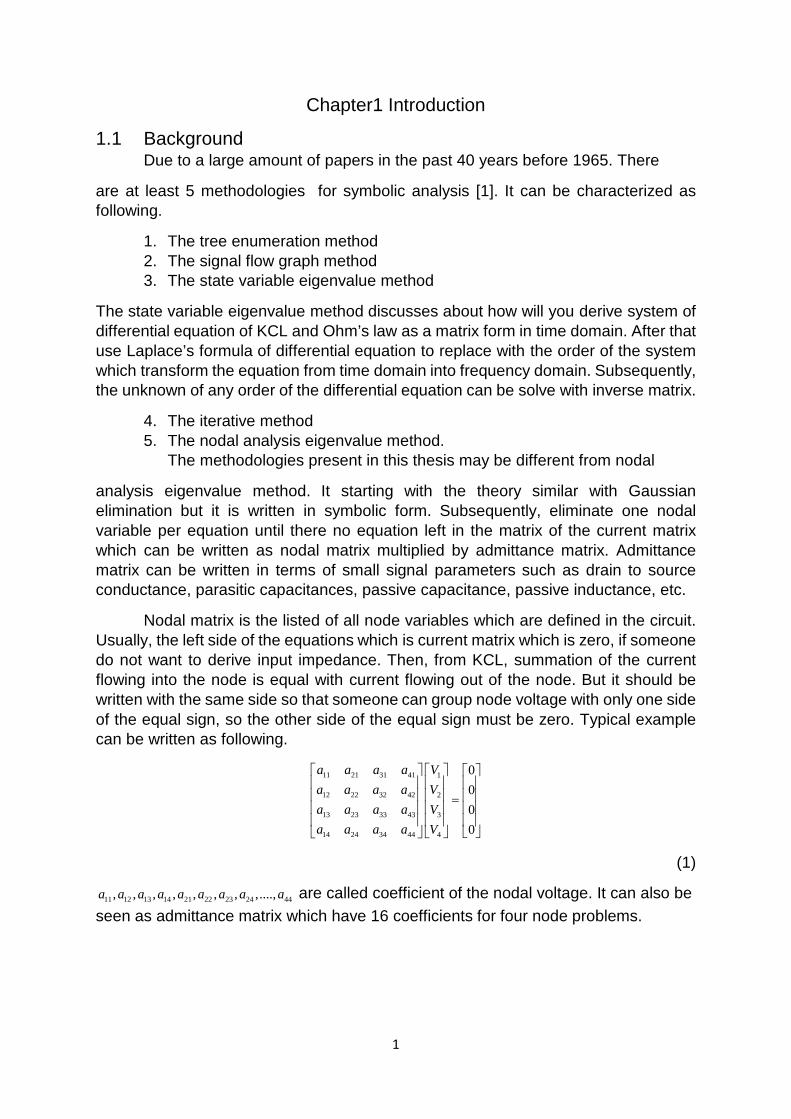
Nodal matrix is the listed of all node variables which are defined in the circuit. Usually, the left side of the equations which is current matrix which is zero, if someone do not want to derive input impedance. Then, from KCL, summation of the current flowing into the node is equal with current flowing out of the node. But it should be written with the same side so that someone can group node voltage with only one side of the equal sign, so the other side of the equal sign must be zero. Typical example can be written as following.
11 21 31 41 1
12 22 32 42 2
13 23 33 43 3
14 24 34 44 4
0000
a a a a Va a a a Va a a a Va a a a V
=
(1)
11 12 13 14 21 22 23 24 44, , , , , , , ,....,a a a a a a a a a are called coefficient of the nodal voltage. It can also be seen as admittance matrix which have 16 coefficients for four node problems.
2
1.2 Thesis Motivation Thesis motivation is created by reading recent advance of electronic circuit in
Journal of Solid state circuits and Transactions on Circuit and Systems, IET Circuit and Devices, electronic letters compared with the references papers therein. Subsequently, it try to determine something different in the methodology of analysis of transfer function of electronic circuit. Usually, novel problem of circuit design methodology start with circuit analysis. By substituting small signal high frequency equivalent circuit of MOSFET into transistor circuit schematic. One can determine closed form transfer function easily by back substitution of nodal voltage as a function of other nodal voltage to eliminate one nodal voltage per equation.
The first motivation is when problem is more and more difficult, because the problem have more than 3 nodes. It might be interesting to derive something called map or route of the solution of back substitution or symbolic Gaussian elimination. Why does it useful? Because it is more systematic, so that the circuit designer do not duplicate back substitute the nodal voltage into other equation iteratively. Some of the electronic circuit analysis problem might have some nodal voltage which have no column duplicate with the same column, so it might be useless to substitute without eliminate one nodal voltage per equation.
The second motivation is to create novel artwork by modification of the old electronic circuit artwork with the hope that the specifications of the circuit looks better that the old circuit such as distributed amplifier, wideband amplifier with the circuit technique called inductive coupling. The process of create novel artwork is to mixed something called passive circuit such as transmission line, passive capacitor, passive resistor, passive inductor with general type of amplifier schematic such as cascade amplifier, folded cascade amplifier, regulated cascade amplifier.
The last motivation is to discuss operation of the presented electronic circuit as detail as possible by imagination and comparative study with the old paper journal which have something related with the presentation such as class of the CMOS oscillator, phase noise analysis which is still in discussion today.
3
1.3 Thesis Contribution My thesis contribution usually originate from artwork. Usually, it is drawn in
Cadence design system. Subsequently, it is redrawn in Microsoft Visio which is the most popular software in drawing electronic circuit schematic.
My first contribution is a modified regulated cascade bandpass amplifier and oscillator which is described in chapter2. The analysis and design methodology and analysis step is described in details in chapter2.
My second contribution is modified simple cross coupled oscillator with current source which is described in chapter3. The analysis and design methodology and analysis step is described in details in chapter3.
My third contribution is two stage operational amplifier with inductive compensation circuit. Analysis of the macro model of the proposed two stage amplifier. Design algorithm of the two stage amplifier with inductive compensation circuit. Equivalent output noise voltage of the presents circuit is described in chapter4.
My fourth contribution is power spectrum of simple cross coupled oscillator by impedance parameter analysis which is described in chapter5.
My fifth contribution is analysis methodology of the circuit which has more than three nodes. Usually, it is difficult to solve circuit which have more than three nodes. But this thesis presents analysis algorithm which is based on symbolic Gaussian elimination which is ideal systematic step. It is not software but it is written derivation report. Currently, the author present how to solve nine node problems which has approximately 47 pages of solution. But without direct electronic circuit analysis method by Kirchhoff’s current law and Ohm’s law and by grouping of nodal voltages in the circuit. The report is useless except to solve for the ratio of the real number instead of complex number as a function of frequency after substitute small signal parameters into the matrix. Another report which should be solved in the future is 12 nodes problem which is the proposed two stage CMOS complementary distributed amplifier.
4
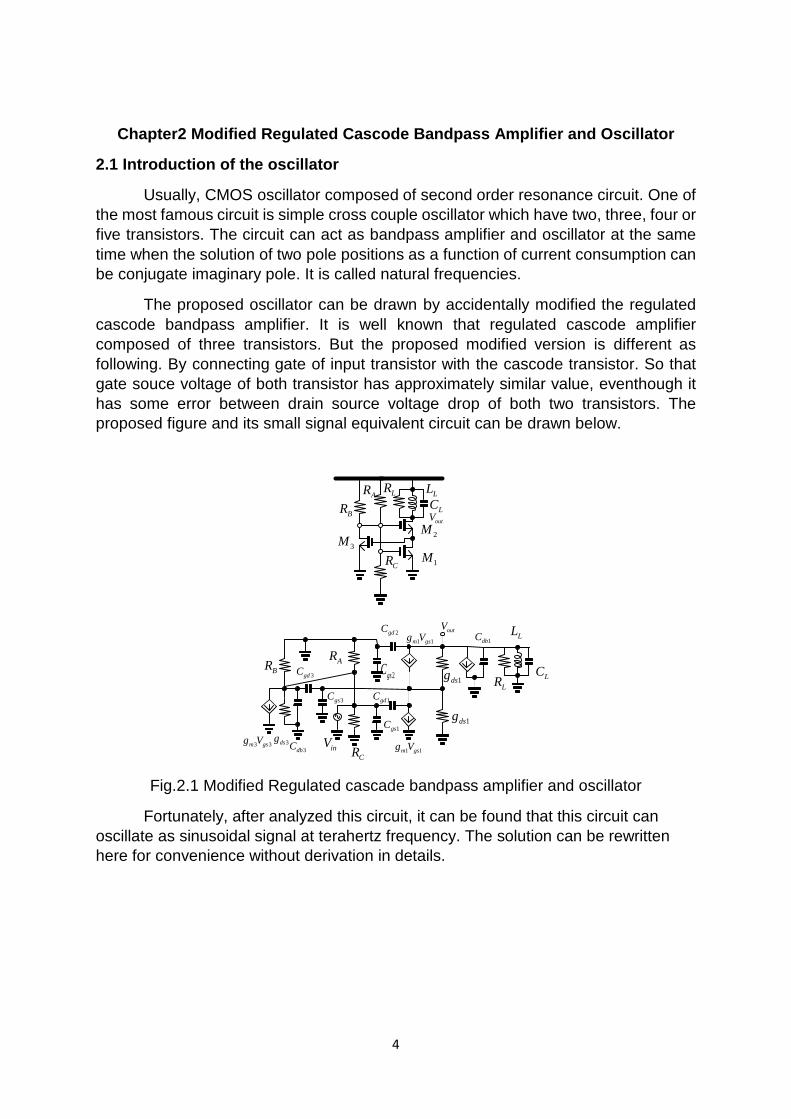
Chapter2 Modified Regulated Cascode Bandpass Amplifier and Oscillator
2.1 Introduction of the oscillator
Usually, CMOS oscillator composed of second order resonance circuit. One of the most famous circuit is simple cross couple oscillator which have two, three, four or five transistors. The circuit can act as bandpass amplifier and oscillator at the same time when the solution of two pole positions as a function of current consumption can be conjugate imaginary pole. It is called natural frequencies.
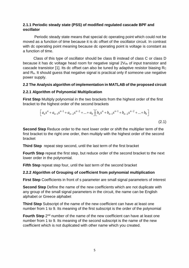
The proposed oscillator can be drawn by accidentally modified the regulated cascode bandpass amplifier. It is well known that regulated cascode amplifier composed of three transistors. But the proposed modified version is different as following. By connecting gate of input transistor with the cascode transistor. So that gate souce voltage of both transistor has approximately similar value, eventhough it has some error between drain source voltage drop of both two transistors. The proposed figure and its small signal equivalent circuit can be drawn below.
1M
2M3M
BRLR
AR
CR
LCLL
inVCR
ARBR
LR
LL
LC
1dsg
1dsg
1 1m gsg V
1 1m gsg V
3 3m gsg V
2gsC
2gdC1dbC
1gdC
1gsC
3gsC
3gdC
3dsg3dbC
outV
outV
Fig.2.1 Modified Regulated cascade bandpass amplifier and oscillator
Fortunately, after analyzed this circuit, it can be found that this circuit can oscillate as sinusoidal signal at terahertz frequency. The solution can be rewritten here for convenience without derivation in details.
5
2.1.1 Periodic steady state (PSS) of modified regulated cascade BPF and oscillator
Periodic steady state means that special dc operating point which could not be moved as a function of time because it is dc offset of the oscillator circuit. In contrast with dc operating point meaning because dc operating point is voltage is constant as a function of time.
Class of this type of oscillator should be class B instead of class C or class D because it has dc voltage head room for negative signal 2Vds of input transistor and cascade transistor [1]. Its dc offset can also be tuned by adaptive resistor biasing RC and Ra. It should guess that negative signal is practical only if someone use negative power supply.
2.2 The Analysis algorithm of implementation in MATLAB of the proposed circuit
2.2.1 Algorithm of Polynomial Multiplication
First Step Multiply polynomial in the two brackets from the highest order of the first bracket to the highest order of the second brackets
1 2 1 21 2 0 1 2 0... ...n n n n n n
n n n n n na s a s a s a b s b s b s b− − − −− − − − + + + + + + + +
(2.1)
Second Step Reduce order to the next lower order or shift the multiplier term of the first bracket to the right one order, then multiply with the highest order of the second bracket
Third Step repeat step second, until the last term of the first bracket
Fourth Step repeat the first step, but reduce order of the second bracket to the next lower order in the polynomial.
Fifth Step repeat step four, until the last term of the second bracket
2.2.2 Algorithm of Grouping of coefficient from polynomial multiplication
First Step Coefficients in front of s parameter are small signal parameters of interest
Second Step Define the name of the new coefficients which are not duplicate with any group of the small signal parameters in the circuit, the name can be English alphabet or Greece alphabet
Third Step Subscript of the name of the new coefficient can have at least one number from 1 to 9. Its meaning of the first subscript is the order of the polynomial
Fourth Step 2nd number of the name of the new coefficient can have at least one number from 1 to 9. Its meaning of the second subscript is the name of the new coefficient which is not duplicated with other name which you created.
6
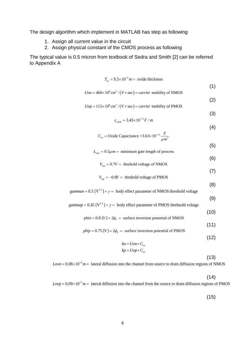
The design algorithm which implement in MATLAB has step as following
1. Assign all current value in the circuit 2. Assign physical constant of the CMOS process as following
The typical value is 0.5 micron from textbook of Sedra and Smith [2] can be referred to Appendix A
99.5 10 oxide thicknessoxT m−= × =
(1) ( )8 2460 10 / sec mobility of NMOSUon cm V carrier= × × =
(2) ( )8 2115 10 / sec mobility of PMOSUop cm V carrier= × × =
(3) 113.45 10 /oxide F mε −= ×
(4) 15
2Oxide Capacitance =3.63 10oxFCmµ
−= ×
(5) min 0.5 minimum gate length of processL mµ= =
(6) 0.7 threhold voltage of NMOStonV V= =
(7) 0.8 threhold voltage of PMOStopV V= − =
(8) 1/20.5 [V ] body effect parameter of NMOS threshold voltagegamman γ= = =
(9) 1/20.45 [V ] body effect parameter of PMOS threhsold voltagegammap γ= = =
(10) 0.8 [ ] 2 surface inversion potential of NMOSFphin V φ= = =
(11) 0.75 [ ] 2 surface inversion potential of PMOSFphip V φ= = =
(12) ox
ox
kn Uon Ckp Uop C
= ×= ×
(13) 60.08 10 lateral diffusion into the channel from source to drain diffusion regions of NMOSLovn m−= × =
(14)
60.09 10 lateral diffusion into the channel from the source to drain diffusion regions of PMOSLovp m−= × =
(15)
7
min
min
22
effN
effP
L L LovnL L Lovp
= − ×
= − ×
(16) 1 2 30, 1, 0sbn sb sbV V V= = =
(17) ( )( )( )( )( )( )
1 1
2 2
3 3
2 2
2 2
2 2
thn ton n f sbn f
thn ton n f sbn f
thn ton n f sbn f
V V V
V V V
V V V
γ φ φ
γ φ φ
γ φ φ
= + + −
= + + −
= + + −
(18)
11 / 1
MJdb
db aV
C CJ ADPB
= × +
(2.1)
( ) 11 / 1
MJSWdb
db bV
C CJSW PDPB
= × +
(2.2) 2
3 3gd gda C C=
(2.3)
( ) ( ) ( )22 2 2 2 2 3 2 3 2 3 2 3 2mb m ds gd db gs gd gd gd m gd ds ma g g g C C C C C C g C g g = − − − + + + + +
(2.4)
( ) ( )( )
2 2 2 2 3 2 3 21
2 3 2 2 2 2 2 3
mb m ds m db gd gd gd
gd m m mb m ds gd ds
g g g g C C C Ca
C g g g g g C g
− − + + + = + − − −
(2.5)
( )0 2 2 2 2 31
mb m ds m dsB
a g g g g gR
= − − +
(2.6)
( )( )3 2 2 3 2 3 2L gd db L db gs gd gdb L C C C C C C C= + + + + +
(2.7)
8
( )
( )
2 2 3
2
3 2 3 2 2 2 2
1
1
L gd db L dsB
L db gs gd gd ds L m gdL
L C C C gR
bL C C C C g L g C
R
+ + +
= + + + + + +
(2.8)
1 2 31 1
L ds dsL B
b L g gR R
= + +
(2.9)
( )0 3 3 2 3 21
ds db gs gd gdB
b g C C C CR
= + + + + +
(2.10)
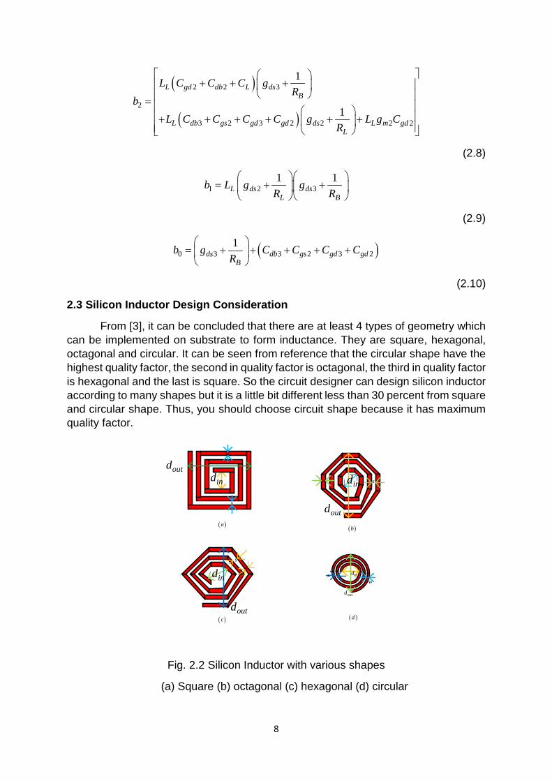
2.3 Silicon Inductor Design Consideration
From [3], it can be concluded that there are at least 4 types of geometry which can be implemented on substrate to form inductance. They are square, hexagonal, octagonal and circular. It can be seen from reference that the circular shape have the highest quality factor, the second in quality factor is octagonal, the third in quality factor is hexagonal and the last is square. So the circuit designer can design silicon inductor according to many shapes but it is a little bit different less than 30 percent from square and circular shape. Thus, you should choose circuit shape because it has maximum quality factor.
indoutd
w
s
( )a ( )b
( )c ( )d
ind
outd
sw
ind
outd
w s
ind
outd
sw
Fig. 2.2 Silicon Inductor with various shapes
(a) Square (b) octagonal (c) hexagonal (d) circular
9
Quality factor of silicon inductor can have at least two definition. From circuit theory point of view, it can be seen from equivalent circuit which can be extracted from experimental results. Quality factor of this view can be seen as imaginary part of input impedance of equivalent circuit divided by real part of equivalent circuit.
Second definition of quality factor can be described as a peak magnetic energy multiply by 2π divided by energy loss in one oscillation cycle.
It can discuss about three methodologies to design silicon inductor with equation. The first methodology is modified Wheeler formula
2
1 021
avgMW
n dL K
Kµ
ρ
= +
(2.3.1) 7
0 4 10 / permeability of free spaceH mµ π −= × =
1 2, layout dependent constantK K =
total turn of silicon inductorn =
( ) ( )1 fill factor= ; 0.1 0.9
nw n sl
ρ ρ+ −
= < <
2in out
avgd dd +
=
For square silicon inductor, if someone want to design 1 nanohenry with modified Wheeler how can he approximate , avgdρ
( )( ) ( )( )
( ) ( )
42 139 7
1 02
4 4
4
6
300 10 8821.59 101 10 2.34 4 101 1 2.75 1 2.75
1 2.75 8821.59 10 8821.59 10 1 2.75 0.9 2.475
3.475 3.938821.59 10
1 2.75 8821.59 10 8821.59 10
avgMW
nn d nL KK
n n
n
n n
µ πρ ρ ρ
ρ
ρ
− −− −
− −
−
−
× × = = × = × = + + +
+ = × → × − = =
= =×
+ = × → ×( ) ( )6
4
1 2.75 0.1 0.275
1.275 1.448821.59 10
n
−
−
− = =
= =×
(2.3.2)
10
( ) ( ) ( )( )
( )
6 6
5 55
3.93 14 10 2.93 4 101 0.9=
5.502 10 1.172 107.415 10
0.9
nw n sl l
l
ρ− −
− −−
× + ×+ −= =
× + ×= = ×
(2.3.3)
The second methodology is based on current sheet approximation, these method is based on many concepts such as geometric mean distance (GMD), arithmetic mean distance (AMD) and arithmetic mean square distance (AMSD). The closed formed formula can be written as following.
21 22
3 4ln2
avgGMD
n d c cL c cµ
ρ ρρ
= + +
(2.3.4)
For square silicon inductor, if someone want to design 1 nanohenry with GMD. It can be shown as a typical example below
( ) ( )( )
[ ]
7 2 62 9
13 2 9
42
4 10 300 10 1.27 2.07ln 0.18 0.13 1 102
if 0.9
2393.89 10 0.8329 0.162 0.1053 10
10 3.7968 1.9485 22633.7577
GMD
GMD
nL
L n
n n
πρ ρ
ρ
ρ
− −−
− −
× × = + + = × =
= × + + =
= = → = ≈
(2.3.5)
The third methodology is data fitted monomial expression, it has five physical variables in this model, and five fitting parameters, it can be rewritten here below
3 51 2 4mono out avgL d w d n sα αα α αβ=
(2.3.6)
For square silicon inductor, if someone want to design 1 nanohenry with this formula, it can be shown as a typical example below
11
( )( ) ( )0
00
tanhtanh
Lin
L
Z Z lZ Z
Z Z lγγ
+=
+
( ) ( )( ) ( )
( ) ( )0 0 0tanh tanhj l j l
in j l j le eZ Z l Z j l Ze e
α β α β
α β α βγ α β
+ − +
+ − +
−= = + =
+
( ) ( ) ( )( ) ( ) ( ) ( )( )( ) ( ) ( )( ) ( ) ( ) ( )( )0
cos sin cos sin
cos sin cos sin
l l
in l l
e l j l e l j lZ Z
e l j l e l j l
α α
α α
β β β β
β β β β
−
−
+ − − = + + −
( ) ( ) ( ) ( ) ( ) ( ) ( ) ( ) ( ) ( )
( ) ( ) ( ) ( ) ( ) ( ) ( ) ( ) ( ) ( )
2 3 4 5 2 3 4 5
0 2 3 4 5 2 3 4 5
1 12 3! 4! 5! 2 3! 4! 5!
1 12 3! 4! 5! 2 3! 4! 5!
in
l l l l l l l ll l
Z Zl l l l l l l l
l l
γ γ γ γ γ γ γ γγ γ
γ γ γ γ γ γ γ γγ γ
− − − − + + + + + − − + + + + = − − − − + + + + + + − + + + +
( ) ( ) ( ) ( ) ( ) ( ) ( ) ( ) ( ) ( )
( ) ( ) ( ) ( ) ( ) ( ) ( ) ( ) ( ) ( )
2 3 4 5 2 3 4 5
0 2 3 4 5 2 3 4 5
1 12 3! 4! 5! 2 3! 4! 5!
1 12 3! 4! 5! 2 3! 4! 5!
in
l l l l l l l ll l
Z Zl l l l l l l l
l l
γ γ γ γ γ γ γ γγ γ
γ γ γ γ γ γ γ γγ γ
+ + + + + − − + − + − = + + + + + + − + − + −
( )3 51 2 4 9 3 1.21 0.147 2.40 1.78 0.03010 1.62 10mono out avg out avgL d w d n s d w d n sα αα α αβ − − − − −= = = ×
(2.3.7)
( )( ) ( ) ( ) ( ) ( ) ( ) ( )
9 3 1.21 0.147 2.40 1.78 0.030log10 log 1.62 10 9
9 2.790 1.21 log 0.147 log 2.40log 1.78log 0.030log
out avg
out avg
d w d n s
d w d n s
− − − − − = × = −
− = − − − + + −
(2.3.8)
2.4 Transmission Line Inductor design based on continue fraction expansion
Transmission line inductor design can be design with well known lossy transmission line which is hyperbolic tangent function of characteristic impedance and length of the transmission line. This equation can be rewritten as following
(2.4.1)
For ideal short circuit termination, then 0LZ = , as a result equation (2.4.1) can be rewritten as following
(2.4.2)
(2.4.3)
(2.4.4)
(2.4.5)
12
( ) ( ) ( ) ( )
( ) ( ) ( )
( ) ( ) ( ) ( )
( ) ( ) ( )
3 5 3 5
0 02 4 2 4
2 ... ...3! 5! ! 3! 5! !
2 1 ... 1 ...2 4! ! 2! 4! !
n odd n odd
in n even n even
l l l l l ll l
n n R j LZ Z Zl l l l l l
n n
γ γ γ γ γ γγ γ
ω γγγ γ γ γ γ γ
= =
= =
+ + + + + + + +
+ = = = + + + + + + + +
( )( ) ( ) ( ) ( )
( ) ( ) ( )
2 4
2 4
1 ...3! 5! !
1 ...2! 4! !
n even
n even
l l ln
ll l l
n
γ γ γ
γ γ γ
=
=
+ + + + + + + +
(2.4.6)
(2.4.7)
( )( ) ( ) ( ) ( )
( ) ( ) ( )
2 4
2 4
1 ...3! 5! !
1 ...2! 4! !
n even
in n even
l l ln
Z Rl j Lll l l
n
γ γ γ
ωγ γ γ
=
=
+ + + + = + + + + +
13
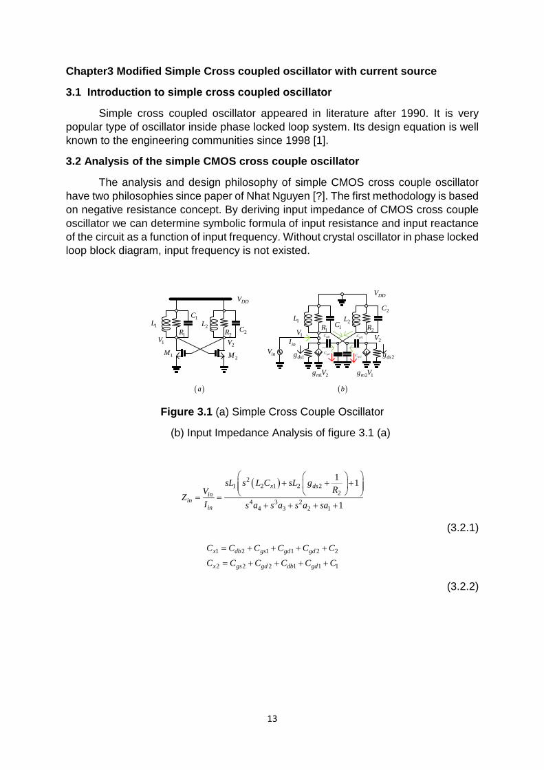
Chapter3 Modified Simple Cross coupled oscillator with current source
3.1 Introduction to simple cross coupled oscillator
Simple cross coupled oscillator appeared in literature after 1990. It is very popular type of oscillator inside phase locked loop system. Its design equation is well known to the engineering communities since 1998 [1].
3.2 Analysis of the simple CMOS cross couple oscillator
The analysis and design philosophy of simple CMOS cross couple oscillator have two philosophies since paper of Nhat Nguyen [?]. The first methodology is based on negative resistance concept. By deriving input impedance of CMOS cross couple oscillator we can determine symbolic formula of input resistance and input reactance of the circuit as a function of input frequency. Without crystal oscillator in phase locked loop block diagram, input frequency is not existed.
1L 2L1C
2C1R 2R
DDV
1M2M
1L 2L1C
2C
1R 2R
DDV
1 2mg V
1dsg
2 1mg V
1gsC2gsC
1gdC 2gdC
2dsg
1V2V
1V2V
inVinI
( )a ( )b Figure 3.1 (a) Simple Cross Couple Oscillator
(b) Input Impedance Analysis of figure 3.1 (a)
( )21 2 1 2 2
24 3 2
4 3 2 1
1 1
1
x dsin
inin
sL s L C sL gRV
ZI s a s a s a sa
+ + + = =
+ + + +
(3.2.1)
1 2 1 1 2 2
2 2 2 1 1 1
x db gs gd gd
x gs gd db gd
C C C C C C
C C C C C C
= + + + +
= + + + +
(3.2.2)
14
( )
( )
24 1 2 2 1 1 2 1 2
3 1 2 2 2 1 2 1 1 1 2 2 1 22 1
2 22 1 2 2 1 1 2 1 2 2 2
1 2
1 1 1 2 21 2
0
1 1 2
1 1
1 1
1
x x gd gd
x ds x ds m gd gd
x x ds ds m
ds ds
a L C L C L C C C
a L C L g L L C g L L g C CR R
a L C L C L L g g L gR R
a L g L gR R
a
= − +
= + + + + +
= + + + + −
= + + +
=
(3.2.3)
( )( )
( ) ( )
3 21 2 1 1 2 2
24 2 3
4 2 1 3
1 1
1
x dsin
inin
j L L C L L gRV
Z s jI a a j a a
ω ωω
ω ω ω ω
− − + + = = =
− + + −
(3.2.4)
Multiply both numerator and denominator with ( ) ( )4 2 34 2 1 31a a j a aω ω ω ω− + − − which is
complex conjugate of denominator so that we can separate symbolic real part and symbolic imaginary part of the input impedance
( )( )
( ) ( )( ) ( )( ) ( )
3 24 2 31 2 1 1 2 2
4 2 1 324 2 3 4 2 3
4 2 1 3 4 2 1 3
111
1 1
x ds
in
j L L C L L ga a j a aR
Z ja a j a a a a j a a
ω ωω ω ω ω
ωω ω ω ω ω ω ω ω
− + − + − + − − = ×
− + + − − + − −
(3.2.5)
( )( ) ( ) ( )( )
( ) ( )
3 2 4 2 31 2 1 1 2 2 4 2 1 3
22 24 2 3
4 2 1 3
11 1
1
x ds
in
j L L C L L g a a j a aR
Z ja a a a
ω ω ω ω ω ω
ωω ω ω ω
− + − + − + − − =
− + + −
(3.2.6)
( )
( )( ) ( )
( )( ) ( )
( ) ( )
3 3 2 4 21 2 1 1 3 1 2 2 4 2
2
3 4 2 2 31 2 1 4 2 1 2 2 1 3
22 24 2 3
4 2 1 3
11 1
11 1
1
x ds
x ds
in
L L C a a L L g a aR
j L L C a a L L g a aR
Z ja a a a
ω ω ω ω ω ω
ω ω ω ω ω ω
ωω ω ω ω
− − + − + − + − − + + − + − =
− + + −
(3.2.7)
From equation (3.2.7) we can separate symbolic resistance and symbolic reactance which are a function of frequency as following
15
( )( )( ) ( )
( ) ( )
3 3 2 4 21 2 1 1 3 1 2 2 4 2
22 24 2 3
4 2 1 3
11 1
1
x ds
in
L L C a a L L g a aR
Ra a a a
ω ω ω ω ω ω
ωω ω ω ω
− − + − + − + =
− + + −
(3.2.8)
( )( )( ) ( )
( ) ( )
3 4 2 2 31 2 1 4 2 1 2 2 1 3
22 24 2 3
4 2 1 3
11 1
1
x ds
in
j L L C a a L L g a aR
Xa a a a
ω ω ω ω ω ω
ωω ω ω ω
− − + + − + − =
− + + −
(3.2.9)
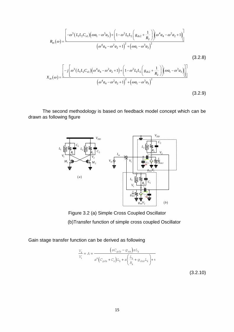
The second methodology is based on feedback model concept which can be drawn as following figure
1L 2L1C
2C1R 2R
DDV
1M2M
2L2C
2R
DDV
2 1mg V
2gsC
2gdC
2dsg
1V2V
2V
inV
inI
( )a1L
1C1R
1 2mg V
1dsg 1gsC
1gdC1V
1V
( )b Figure 3.2 (a) Simple Cross Coupled Oscillator
(b)Transfer function of simple cross coupled Oscillator
Gain stage transfer function can be derived as following
( )( )
gd m
gd ds
sC g sLVA
V Ls C C L s g L
R
−= =
+ + + +
2 2 22
1 2 22 2 2 2 2
2
1
(3.2.10)
16
Feedback stage transfer function can be derived as following
( )( )
gd m
gd ds
sC g sLV
V Ls C C L s g L
R
β−
= =
+ + + +
1 1 11
2 2 11 1 1 1 1
1
1
(3.2.11)
From feedback model concept, the ideal transfer function should be written as following
( )( )
( )( )
( )( )
gd m
gd ds
in
gd m gd m
gd ds gd ds
sC g sL
Ls C C L s g L
RV A
V A
sC g sL sC g sL
L Ls C C L s g L s C C L s g L
R R
β
−
+ + + +
= =+
− − + + + + + + + + +
2 2 2
2 22 2 2 2 2
22
1 1 1 2 2 2
2 21 21 1 1 1 1 2 2 2 2 2
1 2
1
1
1
1 1
(3.2.12)
17
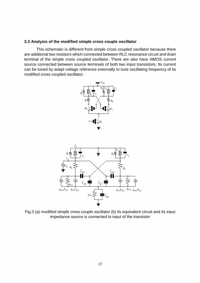
3.3 Analysis of the modified simple cross couple oscillator
This schematic is different from simple cross coupled oscillator because there are additional two resistors which connected between RLC resonance circuit and drain terminal of the simple cross coupled oscillator. There are also have NMOS current source connected between source terminals of both two input transistors. Its current can be tuned by adapt voltage reference externally to tune oscillating frequency of its modified cross coupled oscillator.
1L
2L
1R
2R
1C2C
1M
3M2M
DDV
3R4R
2L
1R
1L
1C 2R2C
3R4R
3gsC2gsC
2gdC
1gdC
3gdC
1dsg
2dsg
3dsg2 2m gsg V 3 3m gsg V
inV
inI
2 2mb bsg V 3 3mb bsg V
Fig.3 (a) modified simple cross couple oscillator (b) its equivalent circuit and its input
impedance source is connected to input of the transistor
18
3.3 Phase noise discussion of the CMOS oscillator
Phase noise can be understood by considering power spectrum. There should have no phase noise for oscillator when the frequency of oscillation is at center frequency. Phase noise usually defined by measure power spectral density of output mean square noise divided by power of carrier signal at phase offset from center frequency. Usually, it can be assume that it has amplitude distortion as a result of self modulation of amplitude due to signal feedback from drain terminal to gate terminal as a typical case of simple cross coupled oscillator. Another case can be seen in simulation results in chapter2 of modified regulated cascode oscillator.
Second reasonable prove is based on flicker noise up conversion due to amplification and modulation of low frequency flicker noise. Which should be prove with mathematics in the ref [1].
Third reasonable prove is based on percentage error of power supply which make current flow into the circuit as constant as possible otherwise the center frequency or frequency of oscillation is fluctuating up and down randomly. The conclusion here is phase noise can be written as a function of power supply fluctuation.
19
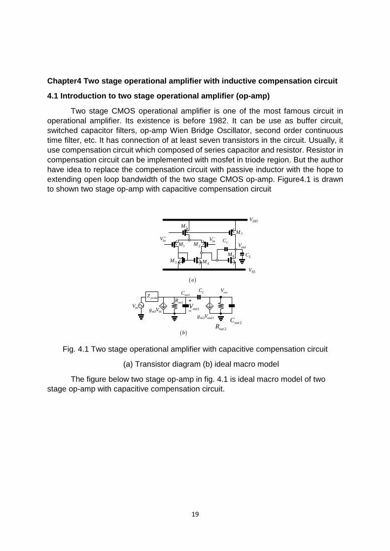
Chapter4 Two stage operational amplifier with inductive compensation circuit
4.1 Introduction to two stage operational amplifier (op-amp)
Two stage CMOS operational amplifier is one of the most famous circuit in operational amplifier. Its existence is before 1982. It can be use as buffer circuit, switched capacitor filters, op-amp Wien Bridge Oscillator, second order continuous time filter, etc. It has connection of at least seven transistors in the circuit. Usually, it use compensation circuit which composed of series capacitor and resistor. Resistor in compensation circuit can be implemented with mosfet in triode region. But the author have idea to replace the compensation circuit with passive inductor with the hope to extending open loop bandwidth of the two stage CMOS op-amp. Figure4.1 is drawn to shown two stage op-amp with capacitive compensation circuit
1M 2M
3M 4M
5M
6M
7M
LC
inV +inV −
outV
DDV
SSV
inV1m ing V
1outR
2outR2 1m outg V
1outC
2outC
1outVprobeZ
outV
CC
CC
( )a
( )b Fig. 4.1 Two stage operational amplifier with capacitive compensation circuit
(a) Transistor diagram (b) ideal macro model
The figure below two stage op-amp in fig. 4.1 is ideal macro model of two stage op-amp with capacitive compensation circuit.
20
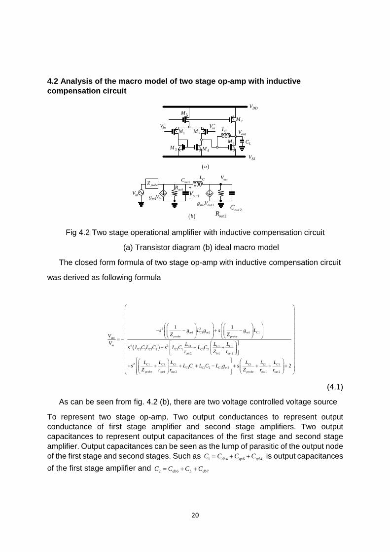
4.2 Analysis of the macro model of two stage op-amp with inductive compensation circuit
1M 2M
3M 4M
5M
6M
7M
LC
inV +inV −
CLoutV
DDV
SSV
inV1m ing V
1outR
2outR
CL
2 1m outg V
1outC
2outC
1outVprobeZ
outV
( )a
( )b Fig 4.2 Two stage operational amplifier with inductive compensation circuit
(a) Transistor diagram (b) ideal macro model
The closed form formula of two stage op-amp with inductive compensation circuit
was derived as following formula
( )
2 21 1 2 1 1
4 3 1 1 11 1 1 2 1 1 1 2
2 1 1
2 1 1 11 1 1 2 1 2
1 2
1 1m C m m C
probe probeout
in C C CC C C C
out in out
C C CC C C m
probe out out
s g L g s g LZ ZV
V L L Ls L C L C s L C L Cr Z r
L L Ls L C L C L gZ r r
− − + − = −
+ + +
+ + + + −
1 1 1
1 2
2C C C
probe out out
L L LsZ r r
+ + + +
(4.1)
As can be seen from fig. 4.2 (b), there are two voltage controlled voltage source
To represent two stage op-amp. Two output conductances to represent output conductance of first stage amplifier and second stage amplifiers. Two output capacitances to represent output capacitances of the first stage and second stage amplifier. Output capacitances can be seen as the lump of parasitic of the output node of the first stage and second stages. Such as 1 4 6 4db gs gdC C C C= + + is output capacitances of the first stage amplifier and 2 6 7db L dbC C C C= + +
21
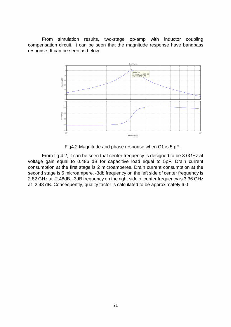
From simulation results, two-stage op-amp with inductor coupling compensation circuit. It can be seen that the magnitude response have bandpass response. It can be seen as below.
Fig4.2 Magnitude and phase response when C1 is 5 pF.
From fig.4.2, it can be seen that center frequency is designed to be 3.0GHz at voltage gain equal to 0.486 dB for capacitive load equal to 5pF. Drain current consumption at the first stage is 2 microamperes. Drain current consumption at the second stage is 5 microampere. -3db frequency on the left side of center frequency is 2.82 GHz at -2.48dB. -3dB frequency on the right side of center frequency is 3.36 GHz at -2.48 dB. Consequently, quality factor is calculated to be approximately 6.0
-30
-25
-20
-15
-10
-5
0
5
System: sysFrequency (Hz): 3.05e+09Magnitude (dB): 0.382
Mag
nitu
de (d
B)
109
1010
45
90
135
180
225
270
Phas
e (d
eg)
Bode Diagram
Frequency (Hz)
22
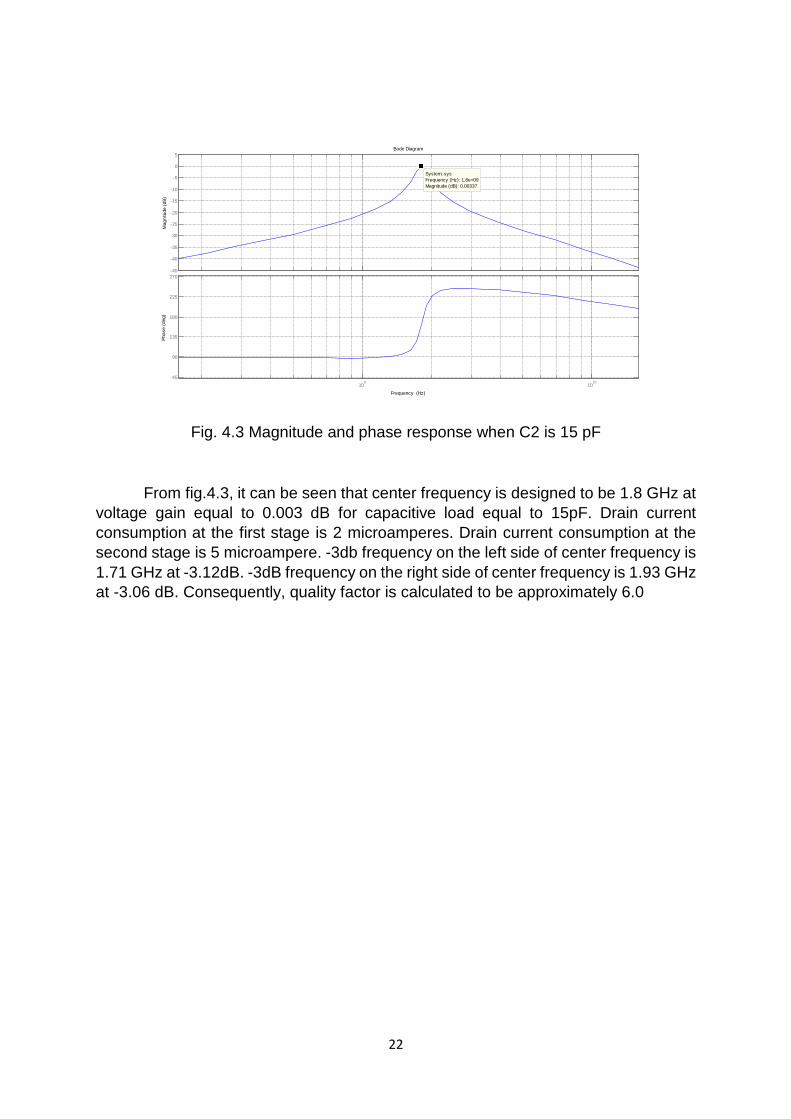
Fig. 4.3 Magnitude and phase response when C2 is 15 pF
From fig.4.3, it can be seen that center frequency is designed to be 1.8 GHz at voltage gain equal to 0.003 dB for capacitive load equal to 15pF. Drain current consumption at the first stage is 2 microamperes. Drain current consumption at the second stage is 5 microampere. -3db frequency on the left side of center frequency is 1.71 GHz at -3.12dB. -3dB frequency on the right side of center frequency is 1.93 GHz at -3.06 dB. Consequently, quality factor is calculated to be approximately 6.0
-45
-40
-35
-30
-25
-20
-15
-10
-5
0
5
System: sysFrequency (Hz): 1.8e+09Magnitude (dB): 0.00337
Mag
nitu
de (d
B)
109
1010
45
90
135
180
225
270
Phas
e (d
eg)
Bode Diagram
Frequency (Hz)
23
Chapter5 CMOS Distributed Amplifier Analysis and Design based on Complementary Regulated Cascode amplifier
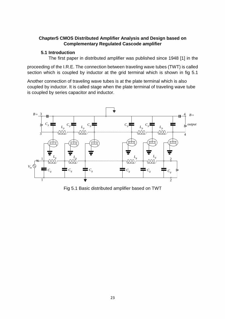
5.1 Introduction The first paper in distributed amplifier was published since 1948 [1] in the
proceeding of the I.R.E. The connection between traveling wave tubes (TWT) is called section which is coupled by inductor at the grid terminal which is shown in fig 5.1
Another connection of traveling wave tubes is at the plate terminal which is also coupled by inductor. It is called stage when the plate terminal of traveling wave tube is coupled by series capacitor and inductor.
inVgC gC gC gC gC
gC
gL gL gL gL
pLpLpL pLpCpC pC pC pC
B + B +4
4
output
3
3
1 2
21 Fig 5.1 Basic distributed amplifier based on TWT
24
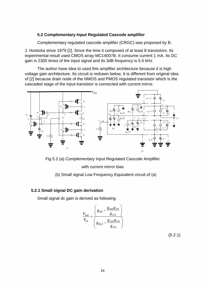
5.2 Complementary Input Regulated Cascode amplifier
Complementary regulated cascode amplifier (CRGC) was proposed by B.
J. Hosticka since 1979 [2]. Since the time it composed of at least 8 transistors. Its experimental result used CMOS array MC14007B. It consume current 1 mA. Its DC gain is 2300 times of the input signal and its 3dB frequency is 5.5 kHz.
The author have idea to used this amplifier architecture because it is high voltage gain architecture. Its circuit is redrawn below. It is different from original idea of [2] because drain node of the NMOS and PMOS regulated transistor which is the cascaded stage of the input transistor is connected with current mirror.
1M
2M
3M
4M
5M
6M
inV
outV
inV
1m ing V
( )2 2 1mg V V−
1dsg
( )4 4 3mg V V−
( )4 30mbg V−
4dsg
( )6 0m ing V −6dsg
outV
1V
3V
7M
8M
1BR
2BR
3, 2, 7D G D
1V
3V
2V2V2V
4V4V
4V8 4mg V
4V4V
2V
7 2mg V
inI2dsg
( )2 10mbg V−
DDV
1BR
2BR
8dsg
5 3mg V5dsg
3 1mg V3dsg
7dsg
2V
( )a
( )b Fig 5.2 (a) Complementary Input Regulated Cascode Amplifier
with current mirror bias
(b) Small signal Low Frequency Equivalent circuit of (a)
5.2.1 Small signal DC gain derivation
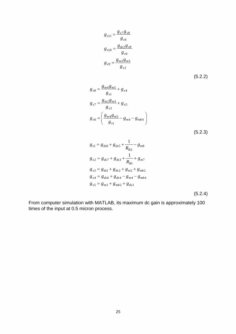
Small signal dc gain is derived as following
6 91
11
10 92
11
m xm
xout
in x xds
x
g gggV
V g ggg
−
=
−
(5.2.1)
25
7 811
6
2 810
6
2 39
2
x xx
x
ds xx
x
m mx
x
g ggg
g ggg
g ggg
=
=
=
(5.2.2)
4 58 4
1
2 37 5
2
4 56 4 4
1
m mx x
x
m mx x
x
m mx m mb
x
g gg gg
g gg gg
g gg g gg
= +
= +
= − −
(5.2.3)
1 8 5 82
2 7 3 71
3 1 2 2 2
4 6 4 4 4
5 2 2 2
1
1
x ds ds mB
x ds ds mB
x ds ds m mb
x ds ds m mb
x m mb ds
g g g gR
g g g gR
g g g g gg g g g gg g g g
= + + −
= + + +
= + + +
= + − −
= + +
(5.2.4)
From computer simulation with MATLAB, its maximum dc gain is approximately 100 times of the input at 0.5 micron process.
26
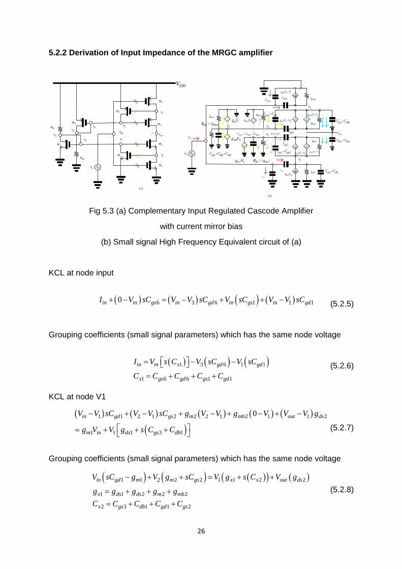
5.2.2 Derivation of Input Impedance of the MRGC amplifier
1M
2M
3M
4M
5M
6M
inV
outV
inV
1m ing V
( )2 2 1mg V V−
1dsg
( )4 4 3mg V V−
( )4 30mbg V−
4dsg
( )6 0m ing V −
6dsg
outV
1V
3V
( )a
( )b
7M
8M
1BR
2BR
5 6gs dbC C+
3 1gs dbC C+
2 4db dbC C+
3, 2, 7D G D
1V
3V
2V2V2V
4V4V
4V
8 4mg V
4V4V
2V
8 8 5gs db dbC C C+ +
7 2mg V
7 7 3gs db dbC C C+ +inI
2dsg
( )2 10mbg V−
DDV
1 7/ /B dsR g
2 8/ /B dsR g
4 5gs gdC C+
2 3gs gdC C+2gdC
4gdC
1gdC
1gsC
5 3mg V5dsg
3 1mg V3dsg
6gsC 6gdC
Fig 5.3 (a) Complementary Input Regulated Cascode Amplifier
with current mirror bias
(b) Small signal High Frequency Equivalent circuit of (a)
KCL at node input
(5.2.5)
Grouping coefficients (small signal parameters) which has the same node voltage
(5.2.6)
KCL at node V1
(5.2.7)
Grouping coefficients (small signal parameters) which has the same node voltage
(5.2.8)
( ) ( ) ( )( ) ( )1 1 2 2 2 1 1 2 2
1 1 2 2 2
2 3 1 1 2
in gd m m gs x x out ds
x ds ds m mb
x gs db gd gs
V sC g V g sC V g s C V g
g g g g gC C C C C
− + + = + +
= + + +
= + + +
( ) ( ) ( ) ( ) ( )
( )1 1 2 1 2 2 2 1 2 1 1 2
1 1 1 3 1
0in gd gs m mb out ds
m in ds gs db
V V sC V V sC g V V g V V V g
g V V g s C C
− + − + − + − + −
= + + +
( ) ( ) ( )1 3 6 1 1
1 6 6 1 1
in in x gd gd
x gs gd gs gd
I V s C V sC V sC
C C C C C
= − − = + + +
( ) ( ) ( ) ( )6 3 6 1 1 10in in gs in gd in gs in gdI V sC V V sC V sC V V sC+ − = − + + −
27
( ) ( )( )( ) ( )
6 6 3 4 5 5 6 6 6 4 4 4
4 4 4 5 4
in gd m gs gd gs db gd ds ds m mb
m gs gd out ds
V sC g V s C C C C C g g g g
V g s C C V g
+ = + + + + + + − −
+ − + −
( ) ( ) ( )( ) ( )6 6 3 4 5 4 4 4 5 4
4 4 5 5 6 6
5 6 4 4 4
in gd m x x m gs gd out ds
x gs gd gs db gd
x ds ds m mb
V sC g V sC g V g s C C V g
C C C C C C
g g g g g
+ = + + − + −
= + + + +
= + − −
( ) ( ) ( )
( )( ) ( )
4 5 5 3 8 4 3 4 4 5
4 8 4 8 8 5 4 42
0
1
ds m m gs gd
ds gs db db out gdB
V g g V g V V V s C C
V g V s C C C V V sCR
− + + + − +
= + + + + + −
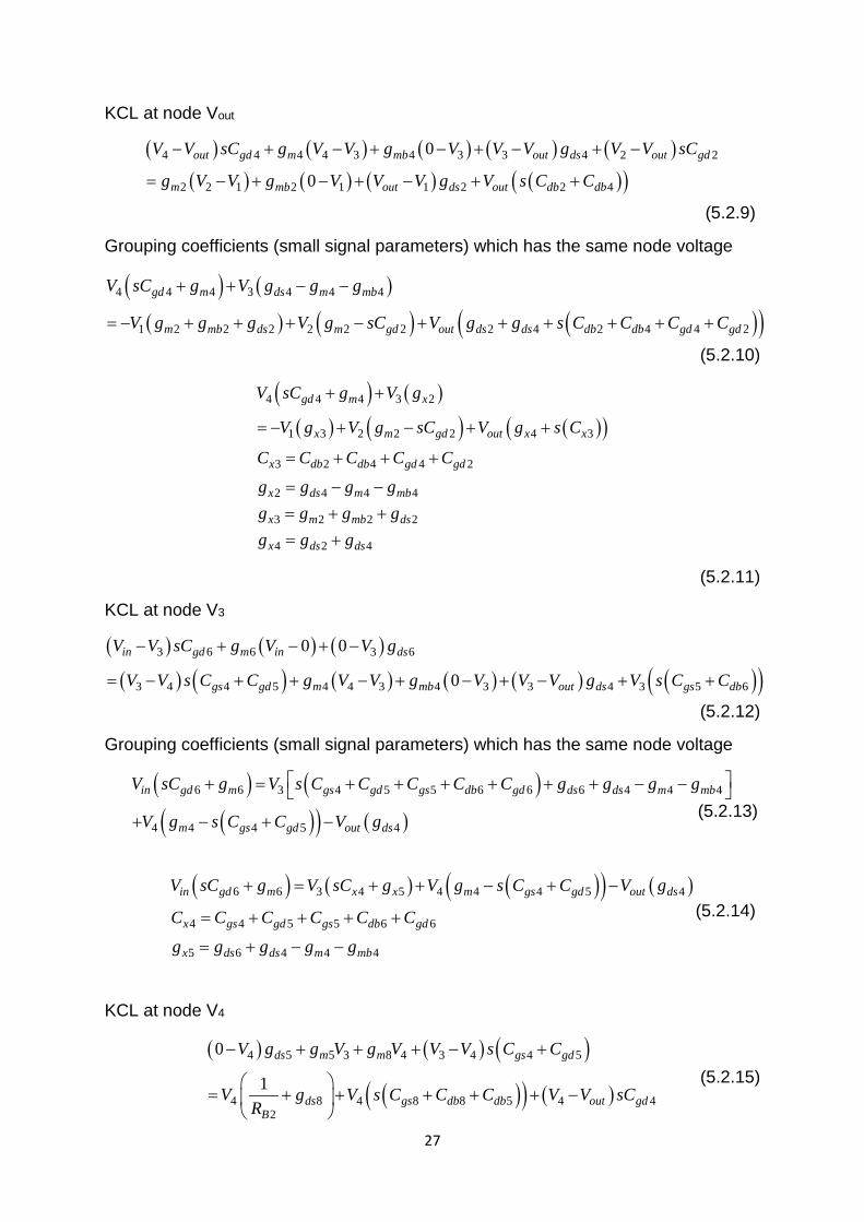
KCL at node Vout
(5.2.9)
Grouping coefficients (small signal parameters) which has the same node voltage
( ) ( )
( ) ( ) ( )( )4 4 4 3 4 4 4
1 2 2 2 2 2 2 2 4 2 4 4 2
gd m ds m mb
m mb ds m gd out ds ds db db gd gd
V sC g V g g g
V g g g V g sC V g g s C C C C
+ + − −
= − + + + − + + + + + +
(5.2.10)
( ) ( )( ) ( ) ( )( )
4 4 4 3 2
1 3 2 2 2 4 3
3 2 4 4 2
2 4 4 4
3 2 2 2
4 2 4
gd m x
x m gd out x x
x db db gd gd
x ds m mb
x m mb ds
x ds ds
V sC g V g
V g V g sC V g s C
C C C C C
g g g gg g g gg g g
+ +
= − + − + +
= + + +
= − −
= + +
= +
(5.2.11)
KCL at node V3
( ) ( ) ( )( ) ( ) ( ) ( ) ( ) ( )( )
3 6 6 3 6
3 4 4 5 4 4 3 4 3 3 4 3 5 6
0 0
0
in gd m in ds
gs gd m mb out ds gs db
V V sC g V V g
V V s C C g V V g V V V g V s C C
− + − + −
= − + + − + − + − + +
(5.2.12)
Grouping coefficients (small signal parameters) which has the same node voltage
(5.2.13)
(5.2.14)
KCL at node V4
(5.2.15)
( ) ( ) ( ) ( ) ( )( ) ( ) ( ) ( )( )
4 4 4 4 3 4 3 3 4 2 2
2 2 1 2 1 1 2 2 4
0
0out gd m mb out ds out gd
m mb out ds out db db
V V sC g V V g V V V g V V sC
g V V g V V V g V s C C
− + − + − + − + −
= − + − + − + +
28
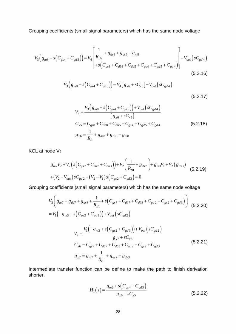
( )( ) ( )
( ) ( ) ( )
7 2 2 7 7 3 2 7 3 1 2 31
2 2 2 1 2 3
1
0
m gs db db ds m dsB
out gd gs gd
g V V s C C C V g g V V gR
V V sC V V s C C
+ + + + + + +
+ − + − + =
( )
( )( ) ( )
2 7 7 3 7 7 3 2 2 31
1 3 2 3 2
1m ds ds gs db db gd gs gd
B
m gs gd out gd
V g g g s C C C C C CR
V g s C C V sC
+ + + + + + + + +
= − + + +
( )( ) ( )1 3 2 3 22
7 6
6 7 7 3 2 2 3
7 7 7 31
1
m gs gd out gd
x x
x gs db db gd gs gd
x m ds dsB
V g s C C V sCV
g sCC C C C C C C
g g g gR
− + + +=
+
= + + + + +
= + + +
( )( ) ( )[ ]
3 8 4 5 44
6 5
5 8 8 5 4 5 4
6 8 5 81
m gs gd out gd
x x
x gs db db gs gd gd
x ds ds mB
V g s C C V sCV
g sCC C C C C C C
g g g gR
+ + +=
+
= + + + + +
= + + −
( )( )8 4 5
16 5
m gs gd
x x
g s C CH s
g sC
+ +=
+
Grouping coefficients (small signal parameters) which has the same node voltage
( )( )( )
( )8 5 823 8 4 5 4 4
8 8 5 4 5 4
1ds ds m
Bm gs gd out gd
gs db db gs gd gd
g g gRV g s C C V V sCs C C C C C C
+ + − + + = −
+ + + + + + (5.2.16)
( )( ) [ ] ( )3 8 4 5 4 6 5 4m gs gd x x out gdV g s C C V g sC V sC+ + = + −
(5.2.17)
(5.2.18)
KCL at node V2
(5.2.19)
Grouping coefficients (small signal parameters) which has the same node voltage
(5.2.20)
(5.2.21)
Intermediate transfer function can be define to make the path to finish derivation shorter.
(5.2.22)
29
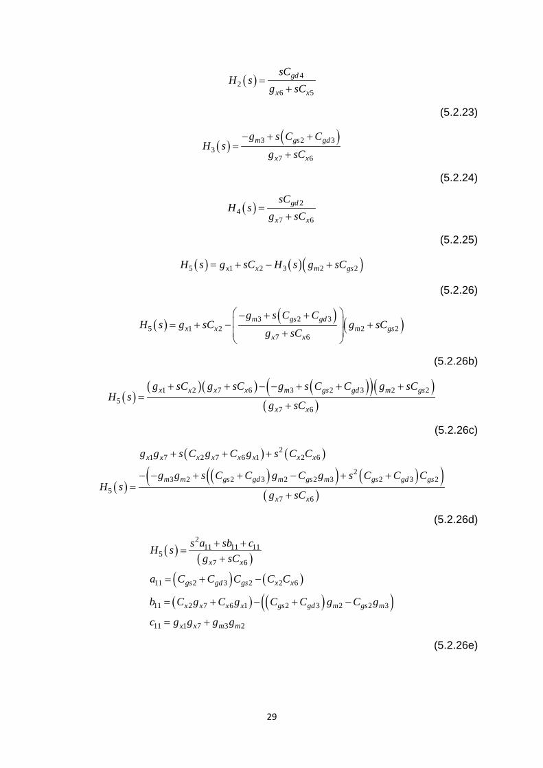
( ) 42
6 5
gd
x x
sCH s
g sC=
+
(5.2.23)
( )( )3 2 3
37 6
m gs gd
x x
g s C CH s
g sC
− + +=
+
(5.2.24)
( ) 24
7 6
gd
x x
sCH s
g sC=
+
(5.2.25)
( ) ( )( )5 1 2 3 2 2x x m gsH s g sC H s g sC= + − +
(5.2.26)
( )( ) ( )3 2 3
5 1 2 2 27 6
m gs gdx x m gs
x x
g s C CH s g sC g sC
g sC
− + + = + − + +
(5.2.26b)
( )( )( ) ( )( )( )
( )1 2 7 6 3 2 3 2 2
57 6
x x x x m gs gd m gs
x x
g sC g sC g s C C g sCH s
g sC
+ + − − + + +=
+
(5.2.26c)
( )
( ) ( )
( )( ) ( )( )( )
21 7 2 7 6 1 2 6
23 2 2 3 2 2 3 2 3 2
57 6
x x x x x x x x
m m gs gd m gs m gs gd gs
x x
g g s C g C g s C C
g g s C C g C g s C C CH s
g sC
+ + +
− − + + − + +=
+
(5.2.26d)
( ) ( )( ) ( )
( ) ( )( )
211 11 11
57 6
11 2 3 2 2 6
11 2 7 6 1 2 3 2 2 3
11 1 7 3 2
x x
gs gd gs x x
x x x x gs gd m gs m
x x m m
s a sb cH sg sC
a C C C C C
b C g C g C C g C g
c g g g g
+ +=
+
= + −
= + − + −
= +
(5.2.26e)
30
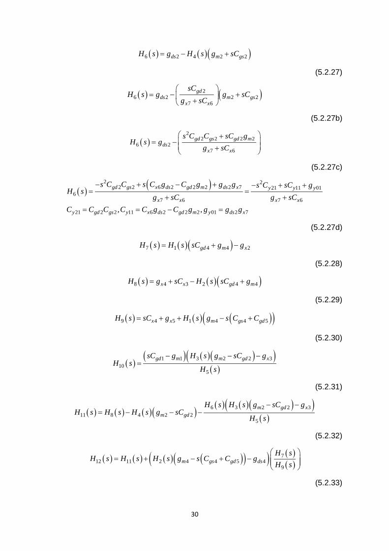
( ) ( )( )6 2 4 2 2ds m gsH s g H s g sC= − +
(5.2.27)
( ) ( )26 2 2 2
7 6
gdds m gs
x x
sCH s g g sC
g sC
= − + +
(5.2.27b)
( )2
2 2 2 26 2
7 6
gd gs gd mds
x x
s C C sC gH s g
g sC
+ = − +
(5.2.27c)
( )( )2 2
2 2 6 2 2 2 2 7 21 11 016
7 6 7 6
21 2 2 11 6 2 2 2 01 2 7, ,
gd gs x ds gd m ds x y y y
x x x x
y gd gs y x ds gd m y ds x
s C C s C g C g g g s C sC gH s
g sC g sCC C C C C g C g g g g
− + − + − + += =
+ +
= = − =
(5.2.27d)
( ) ( )( )7 1 4 4 2gd m xH s H s sC g g= + −
(5.2.28)
( ) ( )( )8 4 3 2 4 4x x gd mH s g sC H s sC g= + − +
(5.2.29)
( ) ( ) ( )( )9 4 5 1 4 4 5x x m gs gdH s sC g H s g s C C= + + − +
(5.2.30)
( )( ) ( )( )( )
( )1 1 3 2 2 3
105
gd m m gd xsC g H s g sC gH s
H s
− − −=
(5.2.31)
( ) ( ) ( )( )( ) ( )( )( )
( )6 3 2 2 3
11 8 4 2 25
m gd xm gd
H s H s g sC gH s H s H s g sC
H s
− −= − − −
(5.2.32)
( ) ( ) ( ) ( )( )( ) ( )( )
712 11 2 4 4 5 4
9m gs gd ds
H sH s H s H s g s C C g
H s
= + − + −
(5.2.33)
31
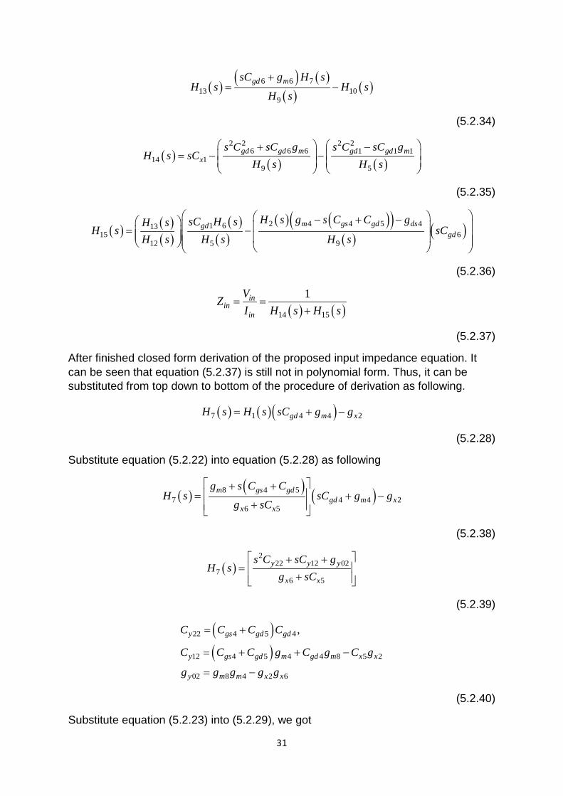
( )( ) ( )
( ) ( )6 6 713 10
9
gd msC g H sH s H s
H s
+= −
(5.2.34)
( ) ( ) ( )
2 2 2 26 6 6 1 1 1
14 19 5
gd gd m gd gd mx
s C sC g s C sC gH s sC
H s H s
+ − = − −
(5.2.35)
( ) ( )( )
( )( )
( ) ( )( )( ) ( )2 4 4 5 41 613
15 612 5 9
m gs gd dsgdgd
H s g s C C gsC H sH sH s sC
H s H s H s
− + − = −
(5.2.36)
( ) ( )14 15
1inin
in
VZI H s H s
= =+
(5.2.37)
After finished closed form derivation of the proposed input impedance equation. It can be seen that equation (5.2.37) is still not in polynomial form. Thus, it can be substituted from top down to bottom of the procedure of derivation as following.
( ) ( )( )7 1 4 4 2gd m xH s H s sC g g= + −
(5.2.28)
Substitute equation (5.2.22) into equation (5.2.28) as following
( )( ) ( )8 4 5
7 4 4 26 5
m gs gdgd m x
x x
g s C CH s sC g g
g sC
+ + = + −
+
(5.2.38)
( )2
22 12 027
6 5
y y y
x x
s C sC gH s
g sC
+ +=
+
(5.2.39)
( )( )
22 4 5 4
12 4 5 4 4 8 5 2
02 8 4 2 6
,y gs gd gd
y gs gd m gd m x x
y m m x x
C C C C
C C C g C g C g
g g g g g
= +
= + + −
= −
(5.2.40)
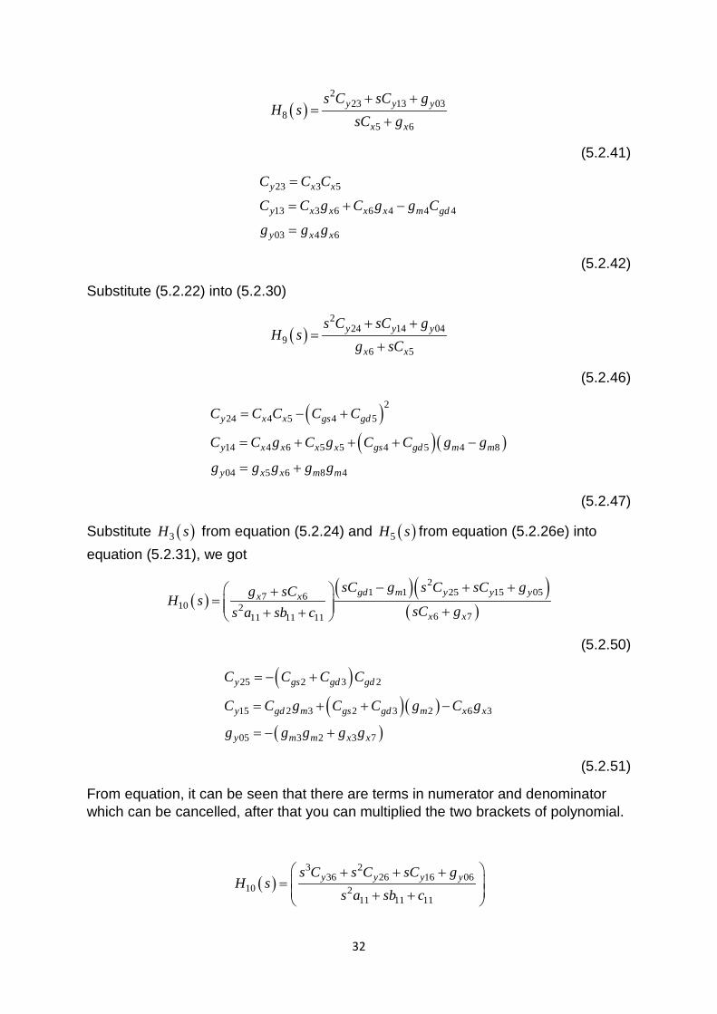
Substitute equation (5.2.23) into (5.2.29), we got
32
( )2
23 13 038
5 6
y y y
x x
s C sC gH s
sC g+ +
=+
(5.2.41)
23 3 5
13 3 6 6 4 4 4
03 4 6
y x x
y x x x x m gd
y x x
C C C
C C g C g g C
g g g
=
= + −
=
(5.2.42)
Substitute (5.2.22) into (5.2.30)
( )2
24 14 049
6 5
y y y
x x
s C sC gH s
g sC+ +
=+
(5.2.46)
( )( )( )
224 4 5 4 5
14 4 6 5 5 4 5 4 8
04 5 6 8 4
y x x gs gd
y x x x x gs gd m m
y x x m m
C C C C C
C C g C g C C g g
g g g g g
= − +
= + + + −
= +
(5.2.47)
Substitute ( )3H s from equation (5.2.24) and ( )5H s from equation (5.2.26e) into equation (5.2.31), we got
( )( )( )
( )
21 1 25 15 057 6
10 26 711 11 11
gd m y y yx x
x x
sC g s C sC gg sCH ssC gs a sb c
− + + += ++ +
(5.2.50)
( )( )( )
( )
25 2 3 2
15 2 3 2 3 2 6 3
05 3 2 3 7
y gs gd gd
y gd m gs gd m x x
y m m x x
C C C C
C C g C C g C g
g g g g g
= − +
= + + −
= − +
(5.2.51)
From equation, it can be seen that there are terms in numerator and denominator which can be cancelled, after that you can multiplied the two brackets of polynomial.
( )3 2
36 26 16 0610 2
11 11 11
y y y ys C s C sC gH s
s a sb c
+ + + = + +
33
(5.2.52)
36 1 25
26 1 15 1 25
16 1 05 1 15
06 1 05
y gd y
y gd y m y
y gd y m y
y m y
C C C
C C C g C
C C g g C
g g g
=
= −
= −
= −
(5.2.53)
From equation (5.2.32), it can be seen that there are five polynomials which are called intermediate transfer function. Manipulate groups of polynomial in the bracket so that it can be written in polynomial form before multiply with other brackets.
( ) ( ) ( )( )( ) ( )( )( )
( )6 3 2 2 3
11 8 4 2 25
m gd xm gd
H s H s g sC gH s H s H s g sC
H s
− −= − − −
(5.2.32)
( ) ( ) ( )( ) ( )( ) ( )6
11 8 4 2 2 165
m gdH s
H s H s H s g sC H sH s
= − − −
(5.2.54)
( ) ( )( )( )2
23 13 0316 3 2 2 3
7 6m gd x
x x
s d sd dH s H s g sC gg sC+ +
= = − −+
(5.2.55)
( )( )
23 2 3 2
13 2 3 2 2 3
03 3 2
gs gd gd
gs gd m gd m
m m
d C C C
d C C g C g
d g g
= − +
= + +
= −
(5.2.56)
Next step, ( )( )
6
5
H sH s
can be defined as following
( ) ( )( )
2 221 11 01 21 11 016 7 6
17 2 25 7 611 11 11 11 11 11
y y y y y yx x
x x
s C sC g s C sC gH s g sCH sH s g sCs a sb c s a sb c
− + + − + + + = = = ++ + + +
(5.2.57)
After that, ( ) ( )17 16H s H s can be defined as following
34
( ) ( ) ( )2 2
21 11 01 23 13 0318 17 16 2
7 611 11 11
y y y
x x
s C sC g s d sd dH s H s H sg sCs a sb c
− + + + + = = ++ +
(5.2.58)
( )4 3 2
44 34 24 14 0418 3 2
35 25 15 05
s d s d s d sd dH ss d s d sd d
+ + + += + + +
(5.2.59)
Coefficients of equation (5.2.59) can be defined as following
44 21 23
34 21 13 11 23
24 21 03 11 13 01 23
14 11 03 01 13
04 01 03
35 11 6
25 11 6 11 7
15 11 7 11 6
05 11 7
y
y y
y y y
y y
y
x
x x
x x
x
d C d
d C d C d
d C d C d g d
d C d g d
d g d
d a Cd b C a gd b g c Cd c g
= −
= − +
= − + +
= +
=
=
= +
= +
=
(5.2.60)
Equation (5.2.54) can be rewritten as following
( ) ( ) ( )( ) ( )11 8 4 2 2 18m gdH s H s H s g sC H s= − − −
(5.2.61)
( ) ( )( )2 2
2 219 4 2 2
6 7
gd gd mm gd
x x
s C sC gH s H s g sC
sC g− +
= − =+
(5.2.62)
Substitute equation (5.2.41), (5.2.62) and (5.2.59) respectively into equation (5.2.61)
( )
( )
( )( )( )
6 5 4 3 261 51 41 31 21 11 01
6 5 4 3 262 52 42 32 22 12
6 5 4 3 263 53 43 33 23 13 03
11 3 25 6 6 7 35 25 15 05x x x x
s f s f s f s f s f sf f
s f s f s f s f s f sf
s f s f s f s f s f sf fH s
sC g sC g s d s d sd d
+ + + + + +
− − + + + + + − + + + + + + =
+ + + + +
(5.2.63)
35
Coefficients of equation (5.2.63) can be defined as following
( )( ) ( ) ( )
( ) ( )( )
61 35 23 6
51 35 23 7 13 6 25 23 6
41 35 6 03 13 7 25 23 7 13 6 15 23 6
31 35 03 7 25 6 03 13 7 15 23 7 13 6 05 23 6
21 25 03 7 15 6 03 13 7 05
y x
y x y x y x
x y y x y x y x y x
y x x y y x y x y x y x
y x x y y x
f d C C
f d C g C C d C C
f d C g C g d C g C C d C C
f d g g d C g C g d C g C C d C C
f d g g d C g C g d C
=
= + +
= + + + +
= + + + + +
= + + + ( )( )
23 7 13 6
11 15 03 7 05 6 03 13 7
05 05 03 7
y x y x
y x x y y x
y x
g C C
f d g g d C g C g
f d g g
+
= + +
=
(5.2.64)
( )( )( )( )
262 5 35
2 252 35 2 2 5 6 25 5
2 242 35 2 2 6 25 2 2 5 6 15 5
2 232 25 2 2 6 15 2 2 5 6 05 5
222 15 2 2 6 05 2 2 5 6
12 05 2
gd x
gd m x gd x gd x
gd m x gd m x gd x gd x
gd m x gd m x gd x gd x
gd m x gd m x gd x
gd
f C C d
f d C g C C g d C C
f d C g g d C g C C g d C C
f d C g g d C g C C g d C C
f d C g g d C g C C g
f d C
=
= − −
= + − −
= + − −
= + −
= 2 6m xg g
(5.2.65)
( )( )( )( )( )
63 5 6 44
53 5 6 34 5 7 6 6 44
43 44 6 7 34 5 7 6 6 24 5 6
33 34 6 7 24 5 7 6 6 14 5 6
23 24 6 7 14 5 7 6 6 04 5 6
13 14 6 7 04 5 7 6 6
03 04
x x
x x x x x x
x x x x x x x x
x x x x x x x x
x x x x x x x x
x x x x x x
f C C df C C d C g C g d
f d g g d C g C g d C C
f d g g d C g C g d C C
f d g g d C g C g d C C
f d g g d C g C gf d
=
= + +
= + + +
= + + +
= + + +
= + +
= 6 7x xg g
(5.2.66)
From equation (5.2.63), Coefficients which have the same order can be grouped as folllowing
( )
( ) ( ) ( )( ) ( ) ( ) ( )
( )( )( )
6 5 461 62 63 51 52 53 41 42 43
3 231 32 33 21 22 23 11 12 13 01 03
11 3 25 6 6 7 35 25 15 05x x x x
s f f f s f f f s f f f
s f f f s f f f s f f f f fH s
sC g sC g s d s d sd d
+ − + − − + − − + − − + − − + − − + − =
+ + + + +
(5.2.67)
36
( )( )
( )( )( )6 5 4 3 2
64 54 44 34 24 14 0411 3 2
5 6 6 7 35 25 15 05x x x x
s f s f s f s f s f sf fH s
sC g sC g s d s d sd d
+ + + + + +=
+ + + + +
(5.2.68)
Coefficients of numerator of equation (5.2.68) can be defined as following
64 61 62 63
54 51 52 53
44 41 42 43
34 31 32 33
24 21 22 23
14 11 12 13
04 01 03
f f f ff f f ff f f ff f f ff f f ff f f ff f f
= + −
= − −
= − −
= − −
= − −
= − −
= −
(5.2.69)
Multiply three brackets of denominator polynomial in (5.2.68), we will get
( )( )
( )6 5 4 3 2
64 54 44 34 24 14 0411 5 4 3 2
55 45 35 25 15 05
s f s f s f s f s f sf fH s
s f s f s f s f sf f
+ + + + + +=
+ + + + +
(5.2.70)
Coefficients of denominator of equation (5.2.70) can be defined as following
( )( )( )( )
55 5 6 35
45 5 7 6 6 35 25 5 6
35 35 6 7 5 7 6 6 25 15 5 6
25 25 6 7 5 7 6 6 15 05 5 6
15 15 6 7 5 7 6 6 05
05 05 6 7
x x
x x x x x x
x x x x x x x x
x x x x x x x x
x x x x x x
x x
f C C df C g C g d d C C
f d g g C g C g d d C C
f d g g C g C g d d C C
f d g g C g C g df d g g
=
= + +
= + + +
= + + +
= + +
=
(5.2.71)
37
Equation (5.2.33) can be rewritten as following
( ) ( ) ( ) ( )( )( ) ( )( )
712 11 2 4 4 5 4
9m gs gd ds
H sH s H s H s g s C C g
H s
= + − + −
(5.2.33)
From equation (5.2.33), it can be seen that there are four polynomials which are called intermediate transfer function. Manipulate groups of polynomial in the bracket so that it can be written in polynomial form before multiply with other brackets
( ) ( )( )
222 12 027
19 29 24 14 04
y y y
y y y
s C sC gH sH s
H s s C sC g+ +
= =+ +
(5.2.72)
( )( ) ( )
( ) ( )( )2
4 4 5 4 420 2 4 4 5
5 6
gd gs gd gd mm gs gd
x x
s C C C s C gH s H s g s C C
sC g
− + += = − +
+
(5.2.73)
( )( ) ( )
( ) ( )( )( )4 42
4 4 5 4 64 5
21 2 4 4 5 45 6
gd mgd gs gd ds x
ds xm gs gd ds
x x
C gs C C C s g g
g CH s H s g s C C g
sC g
− + + −
− = = − + −+
(5.2.74)
( ) ( ) ( )4 3 2
41 31 21 11 0122 21 19 3 2
32 22 12 02
s g s g s g sg gH s H s H ss g s g sg g+ + + +
= =+ + +
(5.2.75)
( )( ) ( )
( ) ( )( )
41 22 4 4 5
31 22 4 4 4 5 12 4 4 5
21 22 4 6 12 4 4 4 5 02 4 4 5
11 12 4 6 02 4 4 4 5
01 4 6 02
y gd gs gd
y gd m ds x y gd gs gd
y ds x y gd m ds x y gd gs gd
y ds x y gd m ds x
ds x y
g C C C C
g C C g g C C C C C
g C g g C C g g C g C C C
g C g g g C g g C
g g g g
= − +
= − − + = − − − − + = − + −
= −
(5.2.76)
38
32 24 5
22 24 6 14 5
12 14 6 04 5
02 04 6
y x
y x y x
y x y x
y x
g C C
g C g C C
g C g g C
g g g
=
= +
= +
=
(5.2.77)
Equation (5.2.33) can be rewritten as following
( ) ( ) ( ) ( )
6 5 4 3 4 3 264 54 44 34 41 31 21
224 14 04 11 01
12 11 22 5 4 3 3 255 45 35 32 22 12 02
225 15 05
s f s f s f s f s g s g s gs f sf f sg g
H s H s H ss f s f s f s g s g sg g
s f sf f
+ + + + + + + + + + = + = + + + + + + + + +
(5.2.78)
( )
( )6 5 4 3
64 54 44 34 3 232 22 12 022
24 14 04
5 4 34 3 255 45 3541 31 21
211 01 25 15 05
12 5 4 355 45 35 3 2
32 22225 15 05
s f s f s f s fs g s g sg g
s f sf f
s f s f s fs g s g s gsg g s f sf f
H ss f s f s f
s g s g sgs f sf f
+ + + + + + + + +
+ ++ + + + + + + + =
+ + + + + + +
( )12 02g+
(5.2.79)
( )( )( )( )9 8 7 6 5 4 3 2
93 83 73 63 53 43 33 23 13 0312 5 4 3 2 3 2
55 45 35 25 15 05 32 22 12 02
s g s g s g s g s g s g s g s g sg gH s
s f s f s f s f sf f s g s g sg g
+ + + + + + + + +=
+ + + + + + + +
(5.2.80)
Coefficients of denominator of equation (5.2.80) can be defined as following
93 64 32 41 55
83 64 22 54 32 41 45 31 55
73 64 12 54 22 44 32 41 35 31 45 21 55
63 64 02 54 12 44 22 34 32 41 25 31 35 21 45 11 55
53 54 02 44 12 34 22 24 32 41 15 31 25 2
g f g g fg f g f g g f g fg f g f g f g g f g f g fg f g f g f g f g g f g f g f g fg f g f g f g f g g f g f g
= +
= + + +
= + + + + +
= + + + + + + +
= + + + + + + 1 35 11 45 01 55
43 44 02 34 12 24 22 14 32 41 05 31 15 21 25 11 35 01 45
33 34 02 24 12 14 22 04 32 31 05 21 15 11 25 01 35
23 24 02 14 12 04 22 21 05 11 15 01 25
13 14 02
f g f g fg f g f g f g f g g f g f g f g f g fg f g f g f g f g g f g f g f g fg f g f g f g g f g f g fg f g f
+ +
= + + + + + + + +
= + + + + + + +
= + + + + +
= + 04 12 11 05 01 15
03 04 02 01 05
g g f g fg f g g f
+ +
= +
(5.2.81)
39
Multiply two brackets of denominator polynomial in (5.2.80), we will get
( )( )
( )9 8 7 6 5 4 3 2
93 83 73 63 53 43 33 23 13 0312 8 7 6 5 4 3 2
84 74 64 54 44 34 24 14 04
s g s g s g s g s g s g s g s g sg gH s
s g s g s g s g s g s g s g sg g
+ + + + + + + + +=
+ + + + + + + +
(5.2.82)
Coefficients of denominator of equation (5.2.82) can be defined as following
84 55 32
74 55 22 45 32
64 55 12 45 22 35 32
54 55 02 45 12 35 22 25 32
44 45 02 35 12 25 22 15 32
34 35 02 25 12 15 22 05 32
24 25 02 15 12 05 22
14 15 02 05 12
04 05 02
g f gg f g f gg f g f g f gg f g f g f g f gg f g f g f g f gg f g f g f g f gg f g f g f gg f g f gg f g
=
= +
= + +
= + + +
= + + +
= + + +
= + +
= +
=
(5.2.83)
Equation (5.2.34) can be rewritten as following
( )( ) ( )
( ) ( ) ( ) ( )6 6 713 10 23 10
9
gd msC g H sH s H s H s H s
H s
+= − = −
(5.2.84)
( )( ) 2 3 26 6 22 12 02 35 25 15 05
23 2 224 14 04 24 14 04
gd m y y y
y y y y y y
sC g s C sC g s g s g sg gH ss C sC g s C sC g
+ + + + + + = = + + + +
(5.2.85)
Coefficients of numerator of equation (5.2.85) can be defined as following
35 6 22
25 6 12 6 22
15 6 02 6 12
05 6 02
gd y
gd y m y
gd y m y
m y
g C C
g C C g C
g C g g C
g g g
=
= +
= +
=
(5.2.86)
Substitute equation (5.2.85) and (5.2.52) into equation (5.2.84) as following
40
( ) ( ) ( )3 23 2
36 26 16 0635 25 15 0513 23 10 2 2
24 14 04 11 11 11
y y y y
y y y
s C s C sC gs g s g sg gH s H s H ss C sC g s a sb c
+ + ++ + + = − = − + + + +
(5.2.87)
Multiply both numerator and denominator with ( )( )2 224 14 04 11 11 11y y ys C sC g s a sb c+ + + +
( )
( )( )( )( )
( )( )
3 2 235 25 15 05 11 11 11
3 2 236 26 16 06 24 14 04
13 2 224 14 04 11 11 11
y y y y y y y
y y y
s g s g sg g s a sb c
s C s C sC g s C sC gH s
s C sC g s a sb c
+ + + + +
− + + + + +=
+ + + +
(5.2.88)
( )
( ) ( ) ( )( ) ( ) ( )
( ) ( ) ( )( )
5 4 335 11 35 11 25 11 35 11 25 11 15 11
225 11 15 11 05 11 15 11 05 11 05 11
5 4 336 24 36 14 26 24 36 04 26 14 16 24
226 04 16 14 06 04 16
13
y y y y y y y y y y y y
y y y y y y y
s g a s g b g a s g c g b g a
s g c g b g a s g c g b g c
s C C s C C C C s C g C C C C
s C g C C g g s CH s
+ + + + + + + + + + +
+ + + + +−
+ + + +=
( ) ( )( ) ( ) ( )( ) ( )
04 06 14 06 044 3 2
14 11 24 11 14 11 24 11 14 11 04 11
14 11 04 11 04 11
y y y y y
y y y y y y
y y y
g g C g g
s C a s C b C a s C c C b g a
s C c g b g c
+ +
+ + + + +
+ + +
(5.2.89)
Coefficient of numerator in the first bracket of equation (5.2.89) can be defined as following
56 35 11
46 35 11 25 11
36 35 11 25 11 15 11
26 25 11 15 11 05 11
16 15 11 05 11
06 05 11
g g ag g b g ag g c g b g ag g c g b g ag g c g bg g c
=
= +
= + +
= + +
= +
=
(5.2.90)
Coefficient of numerator in the second bracket of equation (5.2.89) can be defined as following
41
57 36 24
47 36 14 26 24
37 36 04 26 14 16 24
27 26 04 16 14 06 24
17 16 04 06 14
07 06 04
y y
y y y y
y y y y y y
y y y y y y
y y y y
y y
g C C
g C C C C
g C g C C C C
g C g C C g C
g C g g C
g g g
=
= +
= + +
= + +
= +
=
(5.2.91)
Coefficient of denominator in the bracket of equation (5.2.89) can be defined as following
48 14 11
38 24 11 14 11
28 24 11 14 11 04 11
18 14 11 04 11
08 04 11
y
y y
y y y
y y
y
g C a
g C b C a
g C c C b C a
g C c g b
g g c
=
= +
= + +
= +
=
(5.2.92)
Equation (5.2.35) can be rewritten as following
( ) ( ) ( )
2 2 2 26 6 6 1 1 1
14 19 5
gd gd m gd gd mx
s C sC g s C sC gH s sC
H s H s
+ − = − −
(5.2.93)
Substitute (5.2.26e) and (5.2.46) into (5.2.93), we will get
( ) ( ) ( )2 2 2 2
6 6 6 1 1 114 1 6 5 7 62 2
24 14 04 11 11 11
gd gd m gd gd mx x x x x
y y y
s C sC g s C sC gH s sC g sC g sC
s C sC g s a sb c
+ − = − + − + + + + +
(5.2.94)
Multiply both numerator and denominator of equation (5.2.94)
With ( )( )2 224 14 04 11 11 11y y ys C sC g s a sb c+ + + +
42
( ) ( )( )
( )( )( )
( )( )( )
2 214 1 24 14 04 11 11 11
2 26 6 6 2 2
6 5 24 14 04 11 11 11224 14 04
2 21 1 1 2 2
7 6 24 14 04 11 11 11211 11 11
x y y y
gd gd mx x y y y
y y y
gd gd mx x y y y
H s sC s C sC g s a sb c
s C sC gg sC s C sC g s a sb c
s C sC g
s C sC gg sC s C sC g s a sb c
s a sb c
= + + + +
+ − + + + + + + + − − + + + + + + +
(5.2.95)
( )
( )( )( )( )( )( )( )( )
( )( )
2 21 24 14 04 11 11 11
2 2 26 6 6 6 5 11 11 11
2 2 21 1 1 7 6 24 14 04
14 2 224 14 04 11 11 11
x y y y
gd gd m x x
gd gd m x x y y y
y y y
sC s C sC g s a sb c
s C sC g g sC s a sb c
s C sC g g sC s C sC gH s
s C sC g s a sb c
+ + + + − + + + + − − + + + =
+ + + +
(5.2.96)
( )
( ) ( )( )( ) ( )( ) ( )( )
5 41 24 11 1 24 11 1 14 11
31 24 11 1 14 11 1 04 11
21 14 11 1 04 11 1 04 11
5 2 4 2 26 6 11 6 6 11 11 6 6 6 6 5
3 2 26 6 11 6 6
14
x y x y x y
x y x y x y
x y x y x y
gd x gd x gd x gd m x
gd x gd x
s C C a s C C b C C a
s C C c C C b C g a
s C C c C g b s C g c
s C g a s C g b a C g C g C
s C g c C g C
H s
+ + + + + + + +
+ + +
+ + +−
=
( ) ( )( )( )
( )( ) ( )( )
( )
6 6 6 11 6 6 6 11
2 26 6 6 6 5 11 6 6 6 11
6 6 6 11
5 2 4 2 21 6 24 1 6 14 1 7 1 1 6 24
3 2 21 6 04 1 7 1 1 6 14 1
gd m x gd m x
gd x gd m x gd m x
gd m x
gd x y gd x y gd x gd m x y
gd x gd x gd m x y gd
g C b C g g a
s C g C g C c C g g b
s C g g c
s C C C s C C C C g C g C C
s C C g C g C g C C C g
+
+ + + +
+ + −
+ + − −−
( )( )( ) ( )( )
( )( )( )
1 7 24
2 21 7 1 1 6 04 1 1 7 14
1 1 7 04
2 224 14 04 11 11 11
m x y
gd x gd m x y gd m x y
gd m x y
y y y
g C
s C g C g C g C g g C
s C g g g
s C sC g s a sb c
+ − − + −
+ + + +
(5.2.97)
After this step, you can group and define new coefficients as a group of small signal parameters as following
43
( )
( )( )
( )
5 2 21 24 11 6 6 11 1 6 24
2 21 24 11 1 14 11 6 6 11 11 6 6 6 6 542 2
1 6 14 1 7 1 1 6 24
21 24 11 1 14 11 1 04 11 6 6 11
36
14
x y gd x gd x y
x y x y gd x gd x gd m x
gd x y gd x gd m x y
x y x y x y gd x
gd
s C C a C g a C C C
C C b C C a C g b a C g C g Cs
C C C C g C g C C
C C c C C b C g a C g c
s C
H s
− −
+ − − + + − − −
+ + −
+ −
=
( ) ( )( ) ( )( )
( )( ) ( )( )
26 6 6 6 11 6 6 6 11
2 21 6 04 1 7 1 1 6 14 1 1 7 24
21 14 11 1 04 11 6 6 6 6 5 11 6 6 6 112
21 7 1 1 6 04 1 1 7 14
x gd m x gd m x
gd x gd x gd m x y gd m x y
x y x y gd x gd m x gd m x
gd x gd m x y gd m x y
g C g C b C g g a
C C g C g C g C C C g g C
C C c C g b C g C g C c C g g bs
C g C g C g C g g C
+ − − + − − + − + −+− − −
( )( )( )
1 04 11 6 6 6 11 1 1 7 04
2 224 14 04 11 11 11
x y gd m x gd m x y
y y y
s C g c C g g c C g g g
s C sC g s a sb c
+ − +
+ + + +
(5.2.98)
Let us define new coefficients of the numerator polynomial as following
( )( )
( )
2 259 1 24 11 6 6 11 1 6 24
2 21 24 11 1 14 11 6 6 11 11 6 6 6 6 5
49 2 21 6 14 1 7 1 1 6 24
21 24 11 1 14 11 1 04 11 6 6 11
239 6
x y gd x gd x y
x y x y gd x gd x gd m x
gd x y gd x gd m x y
x y x y x y gd x
gd
g C C a C g a C C C
C C b C C a C g b a C g C g Cg
C C C C g C g C C
C C c C C b C g a C g c
g C
= − −
+ − − + = − − −
+ + −
= −( ) ( )( ) ( )( )
( )( ) ( )( )
6 6 6 6 11 6 6 6 11
2 21 6 04 1 7 1 1 6 14 1 1 7 24
21 14 11 1 04 11 6 6 6 6 5 11 6 6 6 11
29 21 7 1 1 6 04 1 1 7 14
x gd m x gd m x
gd x gd x gd m x y gd m x y
x y x y gd x gd m x gd m x
gd x gd m x y gd m x y
g C g C b C g g a
C C g C g C g C C C g g C
C C c C g b C g C g C c C g g bg
C g C g C g C g g C
+ − − + − − + − + −=− − −
( )19 1 04 11 6 6 6 11 1 1 7 04x y gd m x gd m x yg C g c C g g c C g g g
= − +
(5.2.99)
44
From equation (5.2.36) , it can be seen that there are additional two new variables
( ) ( )( )
( )( )
( ) ( )( )( ) ( )
( ) ( )( )
( ) ( ) ( )( ) ( ) ( )
2 4 4 5 41 61315 6
12 5 9
5 4 3 856 57 46 47 36 37 8
226 27 16 17 06 0713
24 4 3 212 48 38 28 18 08
m gs gd dsgdgd
H s g s C C gsC H sH sH s sC
H s H s H s
s g g s g g s g g s g
s g g s g g g gH sH s
H s s g s g s g sg g
− + − = − − + − + − + − + − + −
= = × + + + +
( )( )
( )( )
7 6 5 44 74 64 54 44
3 234 24 14 04
9 8 7 6 593 83 73 63 53
4 3 243 33 23 13 03
221 11 01
17 61 6
25 25 11 11 11
7 6
y y ygd
x xgd
x x
s g s g s g s g
s g s g sg gs g s g s g s g s g
s g s g s g sg g
s C sC gsC
g sCsC H sH s
H s s a sb cg sC
+ + + + + + + +
+ + + + + + + + +
− + + + = = + + +
3 21 21 1 11 1 01
211 11 11
gd y gd y gd ys C C s C C sC g
s a sb c
− + +=
+ +
(5.2.100)
The results of multiplication of numerator of ( )24H s can be seen as following
( )
13 12 11 10 9 8 7131 121 111 101 91 81 71
6 5 4 3 261 51 41 31 21 11 01
24 4 3 2 9 8 7 6 548 38 28 93 83 73 63 53
4 3 218 08 43 33 23 13 03
1
s h s h s h s h s h s h s h
s h s h s h s h s h sh hH s
s g s g s g s g s g s g s g s gsg g s g s g s g sg g
+ + + + + + + + + + + + + = × + + + + + +
+ + + + + + +
(5.2.101)
The coefficients in numerator polynomial of equation (5.2.101) can be defined as following
( )( ) ( )( ) ( ) ( )( ) ( ) ( ) ( )( ) ( ) ( ) ( ) ( )( )
131 56 57 84
121 56 57 74 46 47 84
111 56 57 64 46 47 74 36 37 84
101 56 57 54 46 47 64 36 37 74 26 27 84
91 56 57 44 46 47 54 36 37 64 26 27 74 16 17 84
81 56 57 34
h g g g
h g g g g g g
h g g g g g g g g g
h g g g g g g g g g g g g
h g g g g g g g g g g g g g g g
h g g g g
= −
= − + −
= − + − + −
= − + − + − + −
= − + − + − + − + −
= − + ( ) ( ) ( ) ( )( )
( ) ( ) ( ) ( ) ( )( )
( ) ( ) ( ) ( ) ( )( )
46 47 44 36 37 54 26 27 64 16 17 74
06 07 84
71 56 57 24 46 47 34 36 37 44 26 27 54 16 17 64
06 07 74
61 56 57 14 46 47 24 36 37 34 26 27 44 16 17 54
06 07 64
g g g g g g g g g g g
g g g
h g g g g g g g g g g g g g g g
g g g
h g g g g g g g g g g g g g g g
g g g
− + − + − + −
+ −
= − + − + − + − + −
+ −
= − + − + − + − + −
+ −
(5.2.102)
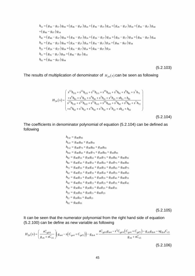
45
( ) ( ) ( ) ( ) ( )( )
( ) ( ) ( ) ( ) ( )( ) ( ) ( ) ( )( ) ( )
51 56 57 04 46 47 14 36 37 24 26 27 34 16 17 44
06 07 54
41 46 47 04 36 37 14 26 27 24 16 17 34 06 07 44
31 36 37 04 26 27 14 16 17 24 06 07 34
21 26 27 04 16 17 14
h g g g g g g g g g g g g g g g
g g g
h g g g g g g g g g g g g g g g
h g g g g g g g g g g g g
h g g g g g g
= − + − + − + − + −
+ −
= − + − + − + − + −
= − + − + − + −
= − + − + ( )( ) ( )( )
06 07 24
11 16 17 04 06 07 14
01 06 07 04
g g g
h g g g g g g
h g g g
−
= − + −
= −
(5.2.103)
The results of multiplication of denominator of ( )24H s can be seen as following
( )
13 12 11 10 9 8 7131 121 111 101 91 81 71
6 5 4 3 261 51 41 31 21 11 01
24 13 12 11 10 9 8 7132 122 112 102 92 82 72
6 5 4 3 262 52 42 32 22 12 02
s h s h s h s h s h s h s h
s h s h s h s h s h sh hH s
s h s h s h s h s h s h s h
s h s h s h s h s h sh h
+ + + + + + + + + + + + +
= + + + + + +
+ + + + + + +
(5.2.104)
The coefficients in denominator polynomial of equation (5.2.104) can be defined as following
132 48 93
122 48 83 38 93
112 48 73 38 83 28 93
102 48 63 38 73 28 83 18 93
92 48 53 38 63 28 73 18 83 08 93
82 48 43 38 53 28 63 18 73 08 83
72 48 33 38 43 28 53 18 63 08 73
h g gh g g g gh g g g g g gh g g g g g g g gh g g g g g g g g g gh g g g g g g g g g gh g g g g g g g g g g
=
= +
= + +
= + + +
= + + + +
= + + + +
= + + + +
62 48 23 38 33 28 43 18 53 08 63
52 48 13 38 23 28 33 18 43 08 53
42 48 03 38 13 28 23 18 33 08 43
32 38 03 28 13 18 23 08 33
22 28 03 18 13 08 23
12 18 03 08 13
02 08 03
h g g g g g g g g g gh g g g g g g g g g gh g g g g g g g g g gh g g g g g g g gh g g g g g gh g g g gh g g
= + + + +
= + + + +
= + + + +
= + + +
= + +
= +
=
(5.2.105)
It can be seen that the numerator polynomial from the right hand side of equation (5.2.100) can be define as new variable as following
( ) ( )( ) ( )24 4 4 4 5 6 4 4 54
26 4 4 5 46 5 6 5
gd m gd gs gd x ds ds xgdm gs gd ds
x x x x
sC g s C C C g g sg CsCH s g s C C g
g sC g sC
− + − − = − + − =
+ +
(5.2.106)
46
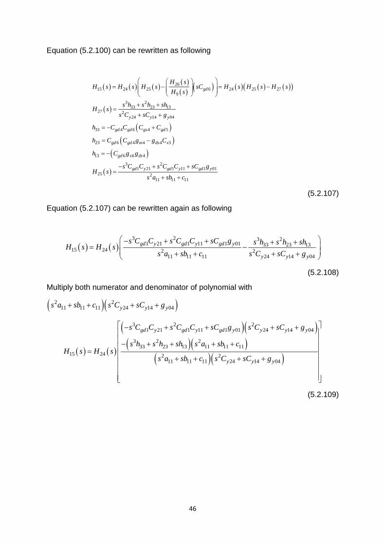
Equation (5.2.100) can be rewritten as following
( ) ( ) ( ) ( )( ) ( ) ( ) ( ) ( )( )
( )
( )( )
( )
( )
2615 24 25 6 24 25 27
9
3 233 23 13
27 224 14 04
33 4 6 4 5
23 6 4 4 4 5
13 6 6 4
3 21 21 1 11 1 01
25 211
gd
y y y
gd gd gs gd
gd gd m ds x
gd x ds
gd y gd y gd y
H sH s H s H s sC H s H s H s
H s
s h s h shH s
s C sC g
h C C C C
h C C g g C
h C g g
s C C s C C sC gH s
s a sb
= − = −
+ +=
+ +
= − +
= −
= −
− + +=
+ 11 11c+
(5.2.107)
Equation (5.2.107) can be rewritten again as following
( ) ( )3 2 3 2
1 21 1 11 1 01 33 23 1315 24 2 2
11 11 11 24 14 04
gd y gd y gd y
y y y
s C C s C C sC g s h s h shH s H ss a sb c s C sC g
− + + + + = − + + + +
(5.2.108)
Multiply both numerator and denominator of polynomial with
( )( )2 211 11 11 24 14 04y y ys a sb c s C sC g+ + + +
( ) ( )
( )( )( )( )
( )( )
3 2 21 21 1 11 1 01 24 14 04
3 2 233 23 13 11 11 11
15 24 2 211 11 11 24 14 04
gd y gd y gd y y y y
y y y
s C C s C C sC g s C sC g
s h s h sh s a sb cH s H s
s a sb c s C sC g
− + + + + − + + + + = + + + +
(5.2.109)
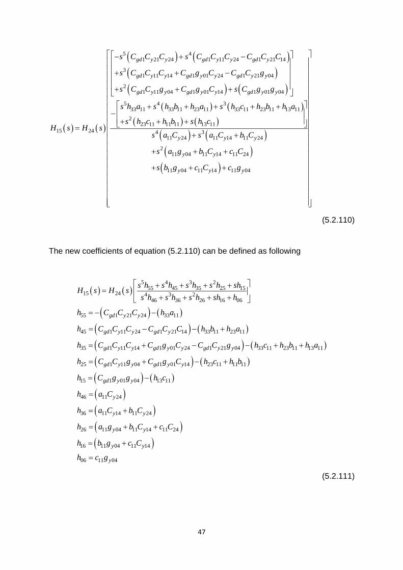
47
( ) ( )
( ) ( )( )( ) ( )
( ) ( )
5 41 21 24 1 11 24 1 21 14
31 11 14 1 01 24 1 21 04
21 11 04 1 01 14 1 01 04
5 4 333 11 33 11 23 11 33 11 23 11 13 11
223
15 24
gd y y gd y y gd y
gd y y gd y y gd y y
gd y y gd y y gd y y
s C C C s C C C C C C
s C C C C g C C C g
s C C g C g C s C g g
s h a s h b h a s h c h b h a
s hH s H s
− + − + + − + + +
+ + + + +−
+=
( ) ( )( ) ( )( )( )
11 11 11 13 114 3
11 24 11 14 11 24
211 04 11 14 11 24
11 04 11 14 11 04
y y y
y y
y y y
c h b s h c
s a C s a C b C
s a g b C c C
s b g c C c g
+ + + + + + + + + +
(5.2.110)
The new coefficients of equation (5.2.110) can be defined as following
( ) ( )
( ) ( )
( ) ( )
( ) ( )
5 4 3 255 45 35 25 15
15 24 4 3 246 36 26 16 06
55 1 21 24 33 11
45 1 11 24 1 21 14 33 11 23 11
35 1 11 14 1 01 24 1 21 04 33 11 23 11 13 11
2
gd y y
gd y y gd y
gd y y gd y y gd y y
s h s h s h s h shH s H ss h s h s h sh h
h C C C h a
h C C C C C C h b h a
h C C C C g C C C g h c h b h a
h
+ + + +=
+ + + +
= − −
= − − +
= + − − + +
( ) ( )
( ) ( )
( )( )( )( )
5 1 11 04 1 01 14 23 11 11 11
15 1 01 04 13 11
46 11 24
36 11 14 11 24
26 11 04 11 14 11 24
16 11 04 11 14
06 11 04
gd y y gd y y
gd y y
y
y y
y y
y y
y
C C g C g C h c h b
h C g g h c
h a C
h a C b C
h a g b C c C
h b g c C
h c g
= + − +
= −
=
= +
= + +
= +
=
(5.2.111)
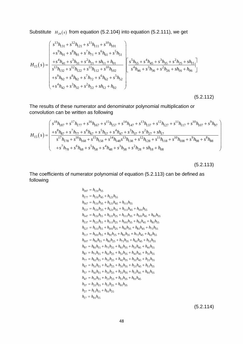
48
Substitute ( )24H s from equation (5.2.104) into equation (5.2.111), we get
( )
13 12 11 10131 121 111 101
9 8 7 6 591 81 71 61 51
4 3 241 31 21 11 01
15 13 12 11 10132 122 112 102
9 8 7 6 592 82 72 62 52
4 3 242 32 22 12 02
s h s h s h s h
s h s h s h s h s h
s h s h s h sh hH ss h s h s h s h
s h s h s h s h s h
s h s h s h sh h
+ + + + + + + + + + + + + = + + +
+ + + + + + + + + +
5 4 3 255 45 35 25 15
4 3 246 36 26 16 06
s h s h s h s h shs h s h s h sh h
+ + + +
+ + + +
(5.2.112)
The results of these numerator and denominator polynomial multiplication or convolution can be written as following
( )
18 17 16 15 14 13 12 11 10 9187 177 167 157 147 137 127 117 107 97
8 7 6 5 4 3 287 77 67 57 47 37 27 17
15 17 16 15 14 13 12 11 10 9 8178 168 158 148 138 128 118 108 98
s h s h s h s h s h s h s h s h s h s h
s h s h s h s h s h s h s h shH ss h s h s h s h s h s h s h s h s h s
+ + + + + + + + +
+ + + + + + + +=
+ + + + + + + + 887 6 5 4 3 2
78 68 58 48 38 28 18 08
h
s h s h s h s h s h s h sh h
+ + + + + + + +
(5.2.113)
The coefficients of numerator polynomial of equation (5.2.113) can be defined as following
187 131 55
177 131 45 121 55
167 131 35 121 45 111 55
157 131 25 121 35 111 45 101 55
147 131 15 121 25 111 35 101 45 91 55
137 121 15 111 25 101 35 91 45 81 55
127 111 15 101 2
h h hh h h h hh h h h h h hh h h h h h h h hh h h h h h h h h h hh h h h h h h h h h hh h h h h
=
= +
= + +
= + + +
= + + + +
= + + + +
= + 5 91 35 81 45 71 55
117 101 15 91 25 81 35 71 45 61 55
107 91 15 81 25 71 35 61 45 51 55
97 81 15 71 25 61 35 51 45 41 55
87 71 15 61 25 51 35 41 45 31 55
77 61 15 51 25 41 3
h h h h h hh h h h h h h h h h hh h h h h h h h h h hh h h h h h h h h h hh h h h h h h h h h hh h h h h h h
+ + +
= + + + +
= + + + +
= + + + +
= + + + +
= + + 5 31 45 21 55
67 51 15 41 25 31 35 21 45 11 55
57 41 15 31 25 21 35 11 45 01 55
47 31 15 21 25 11 35 01 45
37 21 15 11 25 01 35
27 11 15 01 25
17 01 15
h h h hh h h h h h h h h h hh h h h h h h h h h hh h h h h h h h hh h h h h h hh h h h hh h h
+ +
= + + + +
= + + + +
= + + +
= + +
= +
=
(5.2.114)
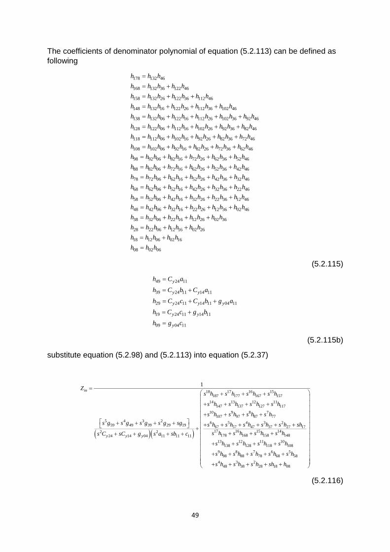
49
The coefficients of denominator polynomial of equation (5.2.113) can be defined as following
178 132 46
168 132 36 122 46
158 132 26 122 36 112 46
148 132 16 122 26 112 36 102 46
138 132 06 122 16 112 26 102 36 92 46
128 122 06 112 16 102 26 92 36 82 46
118 112 06 102 1
h h hh h h h hh h h h h h hh h h h h h h h hh h h h h h h h h h hh h h h h h h h h h hh h h h h
=
= +
= + +
= + + +
= + + + +
= + + + +
= + 6 92 26 82 36 72 46
108 102 06 92 16 82 26 72 36 62 46
98 92 06 82 16 72 26 62 36 52 46
88 82 06 72 16 62 26 52 36 42 46
78 72 06 62 16 52 26 42 36 32 46
68 62 06 52 16 42 26
h h h h h hh h h h h h h h h h hh h h h h h h h h h hh h h h h h h h h h hh h h h h h h h h h hh h h h h h h
+ + +
= + + + +
= + + + +
= + + + +
= + + + +
= + + 32 36 22 46
58 52 06 42 16 32 26 22 36 12 46
48 42 06 32 16 22 26 12 36 02 46
38 32 06 22 16 12 26 02 36
28 22 06 12 16 02 26
18 12 06 02 16
08 02 06
h h h hh h h h h h h h h h hh h h h h h h h h h hh h h h h h h h hh h h h h h hh h h h hh h h
+ +
= + + + +
= + + + +
= + + +
= + +
= +
=
(5.2.115)
49 24 11
39 24 11 14 11
29 24 11 14 11 04 11
19 24 11 14 11
09 04 11
y
y y
y y y
y y
y
h C a
h C b C a
h C c C b g a
h C c g b
h g c
=
= +
= + +
= +
=
(5.2.115b)
substitute equation (5.2.98) and (5.2.113) into equation (5.2.37)
( )( )
18 17 16 15187 177 167 157
14 13 12 11147 137 127 117
10 9 8 7107 97 87 77
5 4 3 2 6 5 4 3 259 49 39 29 19 67 57 47 37 27 17172 2
17824 14 04 11 11 11
1in
y y y
Zs h s h s h s h
s h s h s h s h
s h s h s h s hs g s g s g s g sg s h s h s h s h s h sh
s hs C sC g s a sb c
=+ + +
+ + + +
+ + + + + + + + + + + + + + +
+ + + + 16 15 14168 158 148
13 12 11 10138 128 118 108
9 8 7 6 598 88 78 68 58
4 3 248 38 28 18 08
s h s h s h
s h s h s h s h
s h s h s h s h s h
s h s h s h sh h
+ + + + + + + + + + + + + + + + +
(5.2.116)
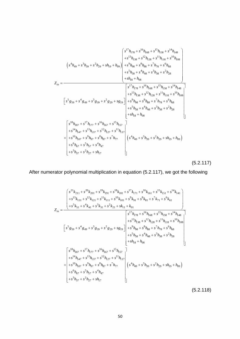
50
( )
17 16 15 14178 168 158 148
13 12 11 10138 128 118 108
4 3 2 9 8 7 649 39 29 19 09 98 88 78 68
5 4 3 258 48 38 28
18 08
5 4 3 259 49 39 29 19
in
s h s h s h s h
s h s h s h s h
s h s h s h sh h s h s h s h s h
s h s h s h s hsh h
Z
s g s g s g s g sg
+ + + + + + +
+ + + + + + + + + + + + + + =
+ + + +
17 16 15 14178 168 158 148
13 12 11 10138 128 118 108
9 8 7 698 88 78 68
5 4 3 258 48 38 28
18 08
18 17 16 15187 177 167 157
14 13 12147 137 127
s h s h s h s h
s h s h s h s h
s h s h s h s h
s h s h s h s hsh h
s h s h s h s h
s h s h s h s
+ + + + + + +
+ + + + + + + + + +
+ + +
+ + + +
+ ( )11
11710 9 8 7 4 3 2
107 97 87 77 49 39 29 19 096 5 4
67 57 473 2
37 27 17
h
s h s h s h s h s h s h s h sh h
s h s h s h
s h s h sh
+ + + + + + + + + + + + + +
(5.2.117)
After numerator polynomial multiplication in equation (5.2.117), we got the following
21 20 19 18 17 16 15 14211 201 191 181 171 161 151 141
13 12 11 10 9 8 7 6131 121 111 101 91 81 71 61
5 4 3 251 41 31 21 11 01
5 4 3 259 49 39 29 19
in
s k s k s k s k s k s k s k s k
s k s k s k s k s k s k s k s k
s k s k s k s k sk kZ
s g s g s g s g sg
+ + + + + + + + + + + + + + + + + + + + + =
+ + + +
17 16 15 14178 168 158 148
13 12 11 10138 128 118 108
9 8 7 698 88 78 68
5 4 3 258 48 38 28
18 08
18 17 16 15187 177 167 157
14 13 12 11147 137 127
s h s h s h s h
s h s h s h s h
s h s h s h s h
s h s h s h s hsh h
s h s h s h s h
s h s h s h s
+ + + + + + + + + + + + + + + + +
+ + +
+ + + +
+ ( )117
10 9 8 7 4 3 2107 97 87 77 49 39 29 19 09
6 5 467 57 47
3 237 27 17
h
s h s h s h s h s h s h s h sh h
s h s h s h
s h s h sh
+ + + + + + + + + + + + + +
(5.2.118)
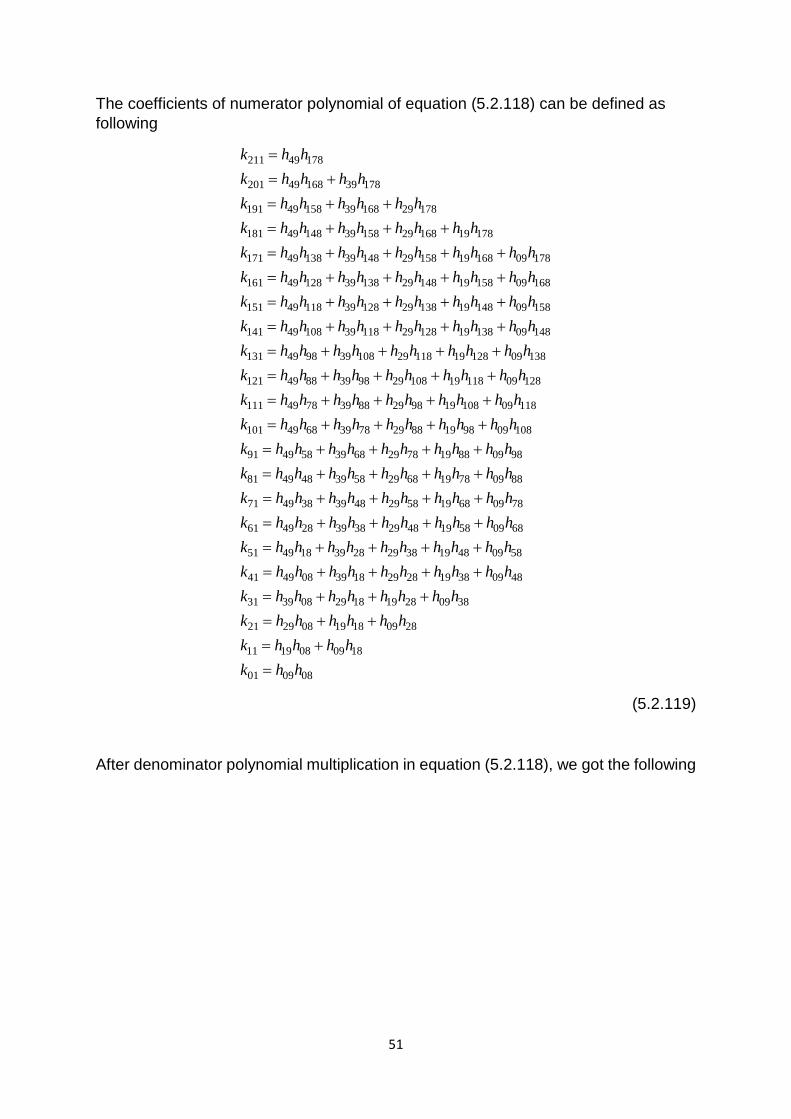
51
The coefficients of numerator polynomial of equation (5.2.118) can be defined as following
211 49 178
201 49 168 39 178
191 49 158 39 168 29 178
181 49 148 39 158 29 168 19 178
171 49 138 39 148 29 158 19 168 09 178
161 49 128 39 138 29 148 19 158 09 168
151 49 118 39
k h hk h h h hk h h h h h hk h h h h h h h hk h h h h h h h h h hk h h h h h h h h h hk h h h
=
= +
= + +
= + + +
= + + + +
= + + + +
= + 128 29 138 19 148 09 158
141 49 108 39 118 29 128 19 138 09 148
131 49 98 39 108 29 118 19 128 09 138
121 49 88 39 98 29 108 19 118 09 128
111 49 78 39 88 29 98 19 108 09 118
1
h h h h h h hk h h h h h h h h h hk h h h h h h h h h hk h h h h h h h h h hk h h h h h h h h h hk
+ + +
= + + + +
= + + + +
= + + + +
= + + + +
01 49 68 39 78 29 88 19 98 09 108
91 49 58 39 68 29 78 19 88 09 98
81 49 48 39 58 29 68 19 78 09 88
71 49 38 39 48 29 58 19 68 09 78
61 49 28 39 38 29 48 19 58 09 68
51 49 18
h h h h h h h h h hk h h h h h h h h h hk h h h h h h h h h hk h h h h h h h h h hk h h h h h h h h h hk h h
= + + + +
= + + + +
= + + + +
= + + + +
= + + + +
= 39 28 29 38 19 48 09 58
41 49 08 39 18 29 28 19 38 09 48
31 39 08 29 18 19 28 09 38
21 29 08 19 18 09 28
11 19 08 09 18
01 09 08
h h h h h h h hk h h h h h h h h h hk h h h h h h h hk h h h h h hk h h h hk h h
+ + + +
= + + + +
= + + +
= + +
= +
=
(5.2.119)
After denominator polynomial multiplication in equation (5.2.118), we got the following
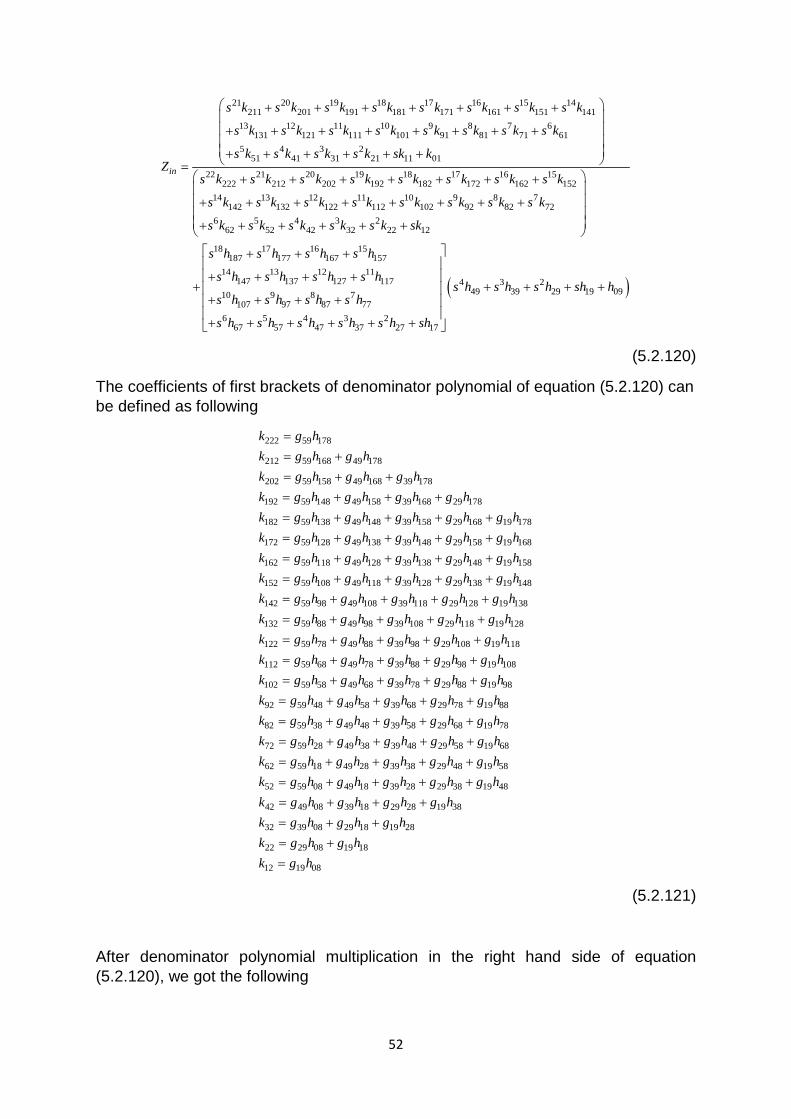
52
21 20 19 18 17 16 15 14211 201 191 181 171 161 151 141
13 12 11 10 9 8 7 6131 121 111 101 91 81 71 61
5 4 3 251 41 31 21 11 01
22 21 20 19222 212 202 192
in
s k s k s k s k s k s k s k s k
s k s k s k s k s k s k s k s k
s k s k s k s k sk kZ
s k s k s k s k
+ + + + + + + + + + + + + + + + + + + + + =
+ + + + 18 17 16 15182 172 162 152
14 13 12 11 10 9 8 7142 132 122 112 102 92 82 72
6 5 4 3 262 52 42 32 22 12
18 17 16 15187 177 167 157
14 13 12 11147 137 127 117
s k s k s k s k
s k s k s k s k s k s k s k s k
s k s k s k s k s k sk
s h s h s h s h
s h s h s h s h
+ + + + + + + + + + + + + + + + +
+ + +
+ + + ++ ( )4 3 2
49 39 29 19 0910 9 8 7107 97 87 77
6 5 4 3 267 57 47 37 27 17
s h s h s h sh hs h s h s h s h
s h s h s h s h s h sh
+ + + + + + + + + + + + + +
(5.2.120)
The coefficients of first brackets of denominator polynomial of equation (5.2.120) can be defined as following
222 59 178
212 59 168 49 178
202 59 158 49 168 39 178
192 59 148 49 158 39 168 29 178
182 59 138 49 148 39 158 29 168 19 178
172 59 128 49 138 39 148 29 158 19 168
162 59 118 49
k g hk g h g hk g h g h g hk g h g h g h g hk g h g h g h g h g hk g h g h g h g h g hk g h g
=
= +
= + +
= + + +
= + + + +
= + + + +
= + 128 39 138 29 148 19 158
152 59 108 49 118 39 128 29 138 19 148
142 59 98 49 108 39 118 29 128 19 138
132 59 88 49 98 39 108 29 118 19 128
122 59 78 49 88 39 98 29 108 19 118
1
h g h g h g hk g h g h g h g h g hk g h g h g h g h g hk g h g h g h g h g hk g h g h g h g h g hk
+ + +
= + + + +
= + + + +
= + + + +
= + + + +
12 59 68 49 78 39 88 29 98 19 108
102 59 58 49 68 39 78 29 88 19 98
92 59 48 49 58 39 68 29 78 19 88
82 59 38 49 48 39 58 29 68 19 78
72 59 28 49 38 39 48 29 58 19 68
62 59 1
g h g h g h g h g hk g h g h g h g h g hk g h g h g h g h g hk g h g h g h g h g hk g h g h g h g h g hk g h
= + + + +
= + + + +
= + + + +
= + + + +
= + + + +
= 8 49 28 39 38 29 48 19 58
52 59 08 49 18 39 28 29 38 19 48
42 49 08 39 18 29 28 19 38
32 39 08 29 18 19 28
22 29 08 19 18
12 19 08
g h g h g h g hk g h g h g h g h g hk g h g h g h g hk g h g h g hk g h g hk g h
+ + + +
= + + + +
= + + +
= + +
= +
=
(5.2.121)
After denominator polynomial multiplication in the right hand side of equation (5.2.120), we got the following
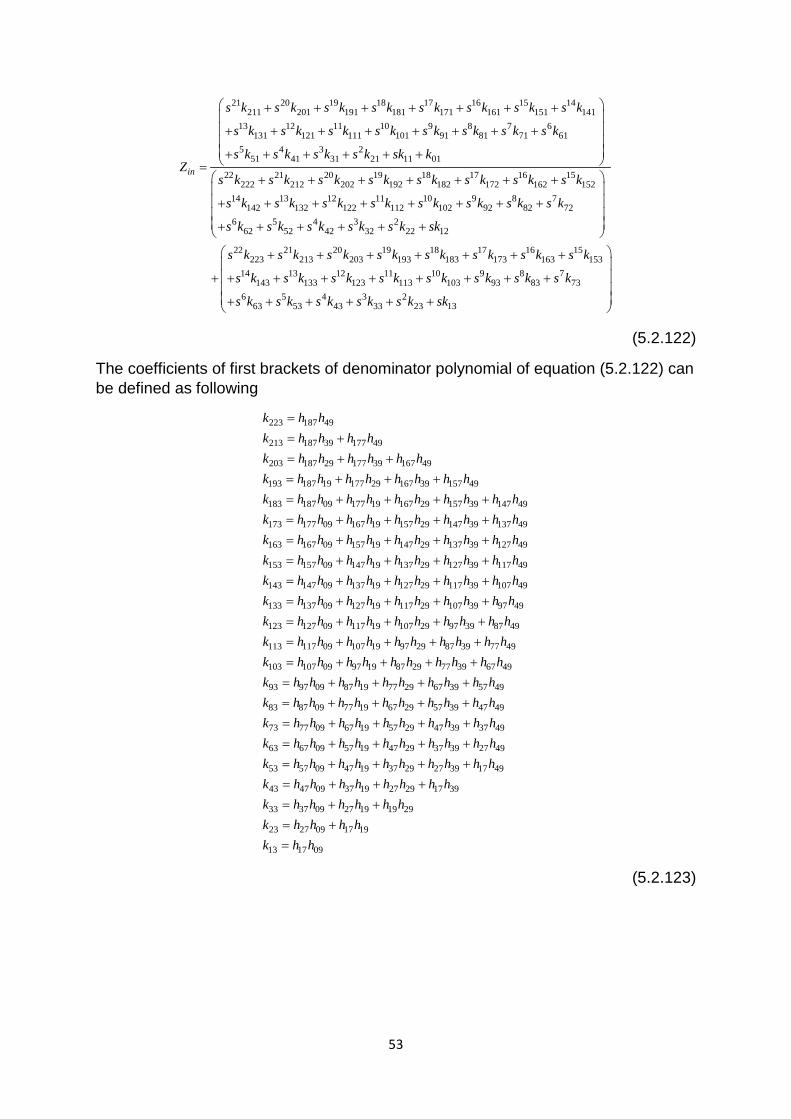
53
21 20 19 18 17 16 15 14211 201 191 181 171 161 151 141
13 12 11 10 9 8 7 6131 121 111 101 91 81 71 61
5 4 3 251 41 31 21 11 01
22 21 20 19222 212 202 192
in
s k s k s k s k s k s k s k s k
s k s k s k s k s k s k s k s k
s k s k s k s k sk kZ
s k s k s k s k
+ + + + + + + + + + + + + + + + + + + + + =
+ + + + 18 17 16 15182 172 162 152
14 13 12 11 10 9 8 7142 132 122 112 102 92 82 72
6 5 4 3 262 52 42 32 22 12
22 21 20 19 18 17 16 15223 213 203 193 183 173 163 153
s k s k s k s k
s k s k s k s k s k s k s k s k
s k s k s k s k s k sk
s k s k s k s k s k s k s k s k
+ + + + + + + + + + + + + + + + +
+ + + + + + +
+ 14 13 12 11 10 9 8 7143 133 123 113 103 93 83 73
6 5 4 3 263 53 43 33 23 13
s k s k s k s k s k s k s k s k
s k s k s k s k s k sk
+ + + + + + + + + + + + + +
(5.2.122)
The coefficients of first brackets of denominator polynomial of equation (5.2.122) can be defined as following
223 187 49
213 187 39 177 49
203 187 29 177 39 167 49
193 187 19 177 29 167 39 157 49
183 187 09 177 19 167 29 157 39 147 49
173 177 09 167 19 157 29 147 39 137 49
163 167 09 15
k h hk h h h hk h h h h h hk h h h h h h h hk h h h h h h h h h hk h h h h h h h h h hk h h h
=
= +
= + +
= + + +
= + + + +
= + + + +
= + 7 19 147 29 137 39 127 49
153 157 09 147 19 137 29 127 39 117 49
143 147 09 137 19 127 29 117 39 107 49
133 137 09 127 19 117 29 107 39 97 49
123 127 09 117 19 107 29 97 39 87 4
h h h h h h hk h h h h h h h h h hk h h h h h h h h h hk h h h h h h h h h hk h h h h h h h h h h
+ + +
= + + + +
= + + + +
= + + + +
= + + + + 9
113 117 09 107 19 97 29 87 39 77 49
103 107 09 97 19 87 29 77 39 67 49
93 97 09 87 19 77 29 67 39 57 49
83 87 09 77 19 67 29 57 39 47 49
73 77 09 67 19 57 29 47 39 37 49
63
k h h h h h h h h h hk h h h h h h h h h hk h h h h h h h h h hk h h h h h h h h h hk h h h h h h h h h hk
= + + + +
= + + + +
= + + + +
= + + + +
= + + + +
= 67 09 57 19 47 29 37 39 27 49
53 57 09 47 19 37 29 27 39 17 49
43 47 09 37 19 27 29 17 39
33 37 09 27 19 19 29
23 27 09 17 19
13 17 09
h h h h h h h h h hk h h h h h h h h h hk h h h h h h h hk h h h h h hk h h h hk h h
+ + + +
= + + + +
= + + +
= + +
= +
=
(5.2.123)
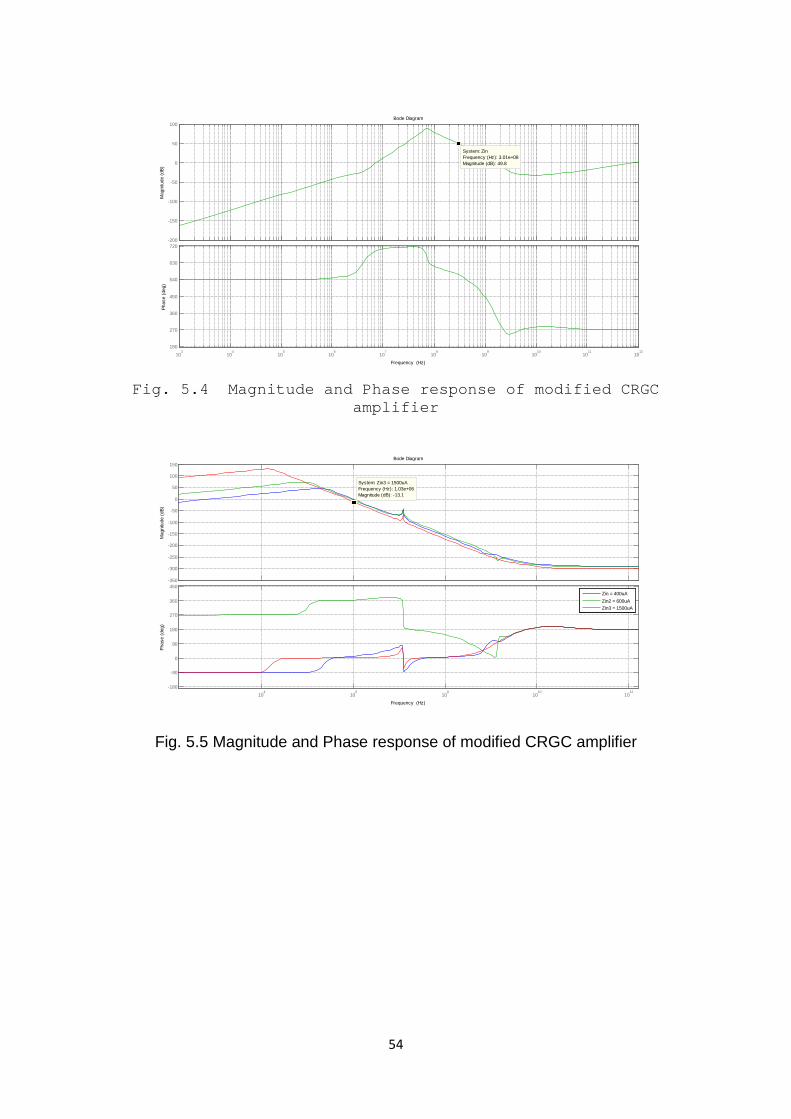
54
Fig. 5.4 Magnitude and Phase response of modified CRGC
amplifier
Fig. 5.5 Magnitude and Phase response of modified CRGC amplifier
-200
-150
-100
-50
0
50
100
System: ZinFrequency (Hz): 3.01e+08Magnitude (dB): 49.8
Mag
nitu
de (d
B)
103
104
105
106
107
108
109
1010
1011
1012
180
270
360
450
540
630
720
Phas
e (d
eg)
Bode Diagram
Frequency (Hz)
-350
-300
-250
-200
-150
-100
-50
0
50
100
150
System: Zin3 = 1500uAFrequency (Hz): 1.03e+06Magnitude (dB): -13.1
Mag
nitu
de (d
B)
104
106
108
1010
1012
-180
-90
0
90
180
270
360
450
Phas
e (d
eg)
Bode Diagram
Frequency (Hz)
Zin = 400uAZin2 = 600uAZin3 = 1500uA
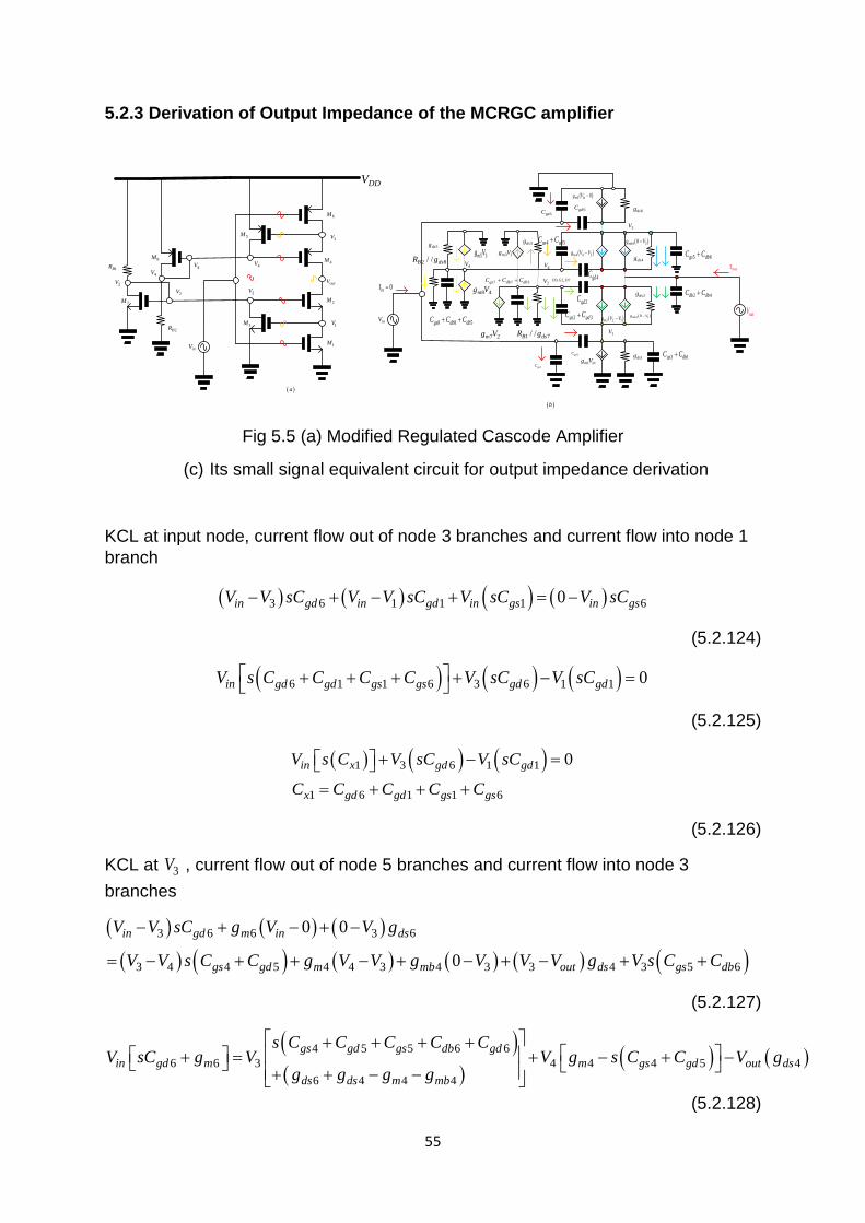
55
5.2.3 Derivation of Output Impedance of the MCRGC amplifier
1M
2M
3M
4M
5M
6M
inV
outV
inV
1m ing V
( )2 2 1mg V V−
1dsg
( )4 4 3mg V V−
( )4 30mbg V−
4dsg
( )6 0m ing V −
6dsg
outV
1V
3V
( )a
( )b
7M
8M
1BR
2BR
5 6gs dbC C+
3 1gs dbC C+
2 4db dbC C+
3, 2, 7D G D
1V
3V
2V2V2V
4V4V
4V
8 4mg V
4V4V
2V
8 8 5gs db dbC C C+ +
7 2mg V
7 7 3gs db dbC C C+ +0inI =
2dsg
( )2 10mbg V−
DDV
1 7/ /B dsR g
2 8/ /B dsR g
4 5gs gdC C+
2 3gs gdC C+2gdC
4gdC
1gdC
1gsC
5 3mg V5dsg
3 1mg V3dsg
6gsC 6gdC
outI
Fig 5.5 (a) Modified Regulated Cascode Amplifier
(c) Its small signal equivalent circuit for output impedance derivation
KCL at input node, current flow out of node 3 branches and current flow into node 1 branch
( ) ( ) ( ) ( )3 6 1 1 1 60in gd in gd in gs in gsV V sC V V sC V sC V sC− + − + = −
(5.2.124)
( ) ( ) ( )6 1 1 6 3 6 1 1 0in gd gd gs gs gd gdV s C C C C V sC V sC + + + + − =
(5.2.125)
( ) ( ) ( )1 3 6 1 1
1 6 1 1 6
0in x gd gd
x gd gd gs gs
V s C V sC V sC
C C C C C
+ − = = + + +
(5.2.126)
KCL at 3V , current flow out of node 5 branches and current flow into node 3 branches
( ) ( ) ( )( ) ( ) ( ) ( ) ( ) ( )
3 6 6 3 6
3 4 4 5 4 4 3 4 3 3 4 3 5 6
0 0
0in gd m in ds
gs gd m mb out ds gs db
V V sC g V V g
V V s C C g V V g V V V g V s C C
− + − + −
= − + + − + − + − + +
(5.2.127)
( )( )
( ) ( )4 5 5 6 66 6 3 4 4 4 5 4
6 4 4 4
gs gd gs db gdin gd m m gs gd out ds
ds ds m mb
s C C C C CV sC g V V g s C C V g
g g g g
+ + + + + = + − + − + + − −
(5.2.128)
56
[ ] ( ) ( )
( )
6 6 3 2 2 4 4 4 5 4
2 4 5 5 6 6
2 6 4 4 4
in gd m x x m gs gd out ds
x gs gd gs db gd
x ds ds m mb
V sC g V sC g V g s C C V g
C C C C C C
g g g g g
+ = + + − + − = + + + +
= + − −
(5.2.129)
KCL at node outV , current flow into node 6 branches and current flow out of node 4 branches
( ) ( ) ( ) ( ) ( )( ) ( ) ( ) ( )( )
4 4 4 4 3 4 3 3 4 2 2
2 2 1 2 1 1 2 2 4
0
0
out gd m mb out ds out gd out
m mb out ds out gd db
V V sC g V V g V V V g V V sC i
g V V g V V V g V s C C
− + − + − + − + − +
= − + − + − + +
(5.2.130)
[ ][ ] ( )
4 4 4 3 4 4 4 2 2 2
1 2 2 2 4 2 2 4 2 4
gd m ds m mb out m gd
m mb ds out gd gd db db ds ds
V sC g V g g g i V g sC
V g g g V s C C C C g g
+ + − − + = − − + + + + + + + +
(5.2.131)
[ ] [ ] [ ]4 4 4 3 4 4 4 2 2 2 1 2 2 2 3 3
3 4 2 2 4
3 2 4
gd m ds m mb out m gd m mb ds out x x
x gd gd db db
x ds ds
V sC g V g g g i V g sC V g g g V sC g
C C C C C
g g g
+ + − − + = − − + + + + = + + +
= +
(5.2.132)
KCL at node 1V , current flow into node 5 branches, current flow out of node 3 branches
( ) ( ) ( ) ( ) ( )
( ) ( )2 1 2 3 2 2 1 2 1 1 2
1 1 1 1 1 3 1
0gs gd m mb out ds
in gd m in ds gs db
V V s C C g V V g V V V g
V V sC g V V g s C C
− + + − + − + −
+ − = + + +
(5.2.133)
( ) ( )
( )
2 3 1 3 12 2 3 2 1
1 2 2 2
2 1 1
gs gd gd gs dbgs gd m
ds m mb ds
out ds in m gd
s C C C C CV s C C g V
g g g g
V g V g sC
+ + + + + + − − − − − + = −
(5.2.134)
( ) [ ] ( )2 2 3 2 1 4 4 2 1 1
4 2 3 1 3 1
4 1 2 2 2
gs gd m x x out ds in m gd
x gs gd gd gs db
x ds m mb ds
V s C C g V sC g V g V g sC
C C C C C C
g g g g g
+ + − + + = − = + + + +
= − − − −
(5.2.135)
57
KCL at node 2V , current flow out of node 7 branches
( )
( ) ( ) ( ) ( )
7 2 2 7 3 7 3 1 2 71
2 1 2 3 2 13 2 2
1
0
m gs db db m dsB
gs gd ds out gd
g V V s C C C g V V gR
V V s C C V g V V sC
+ + + + + + + − + + + − =
(5.2.136)
( ) ( )7 7 3
12 1 3 2 3 2
7 3 7
2 2 3
1
0m ds ds
Bm gs gd out gd
gs db db
gd gs gd
g g gR
V V g s C C V sCC C Cs
C C C
+ + + + − + − = + + + + + +
(5.2.137)
( ) ( ) ( )2 5 5 1 3 2 3 2
5 7 3 7 2 2 3
5 7 7 31
0
1
x x m gs gd out gd
x gs db db gd gs gd
x m ds dsB
V g s C V g s C C V sC
C C C C C C C
g g g gR
+ + − + − = = + + + + +
= + + +
(5.2.138)
KCL at node 4V , current flow into node 4 branches, current flow out of node 3 branches
( ) ( ) ( )
( ) ( )
8 4 5 3 4 5 3 4 4 5
4 8 4 8 5 8 4 42
0
1
m m ds gs gd
ds gs db db out gdB
g V g V V g V V s C C
V g V s C C C V V sCR
+ + − + − + = + + + + + −
(5.2.139)
( ) ( ) ( )3 5 4 5 4
8 5 84 8 5 8
4 5 42
1
m gs gd out gd
gs db dbds ds m
gs gd gdB
V g s C C V sC
C C CV g g g s
C C CR
+ + + + +
= + + − + + + +
(5.2.140)
( ) ( ) ( ) [ ]3 5 4 5 4 4 6 6
6 8 5 82
6 8 5 8 4 5 4
1m gs gd out gd x x
x ds ds mB
x gs db db gs gd gd
V g s C C V sC V g sC
g g g gR
C C C C C C C
+ + + = +
= + + −
= + + + + +
(5.2.141)
58
From equation (5.2.126)
1 61 3
1 1
gd gdin
x x
sC sCV V V
sC sC
= −
(5.2.126b)
From equation (5.2.129)
[ ] ( ) ( )4 4 4 53 2 2 4
6 6 6 6 6 6
m gs gdx x out dsin
gd m gd m gd m
V g s C CV sC g V gV
sC g sC g sC g
− ++ = + −+ + +
(5.2.129b)
Let us define intermediate transfer function to reduce the time to finished the closed form formula as following
( ) ( ) ( )
( ) [ ]
( )( )
( ) ( )
3 4 4 3 5
2 24
6 6
4 4 53
6 6
45
6 6
in out
x x
gd m
m gs gd
gd m
ds
gd m
V V H s V H s V H s
sC gH s
sC g
g s C CH s
sC g
gH s
sC g
= + −
+=
+
− + =+
=+
(5.2.129c)
From equation (5.2.135)
( ) ( ) [ ]2 2 3 2 1 4 4 2
1 1 1 1 1 1
gs gd m x x out dsin
m gd m gd m gd
V s C C g V s C g V gV
g sC g sC g sC
+ + + = − +− − −
(5.2.135b)
From equation (5.2.141)
( ) ( )3 5 4 5 44
6 6 6 6
m gs gd out gd
x x x x
V g s C C V sCV
sC g sC g
+ + = ++ +
(5.2.141b)
Let us define intermediate transfer function to reduce the time to finished the closed form formula as following
59
( ) ( )
( )( )
( )( )
4 3 1 2
5 4 51
6 6
42
6 6
out
m gs gd
x x
gd
x x
V V H s V H s
g s C CH s
sC g
sCH s
sC g
= +
+ + =+
=+
(5.2.141c)
Substitute equation (5.2.141c) into (5.2.129c)
( ) ( ) ( ) ( ) ( )3 4 3 1 2 3 5in out outV V H s V H s V H s H s V H s= + + −
(5.2.129c)
After grouping the coefficients which have the same node voltage, we get
( ) ( ) ( ) ( ) ( ) ( )3 4 1 3 2 3 5in outV V H s H s H s V H s H s H s= + + −
(5.2.129d)
From equation (5.2.132), it can be rewritten here
( ) ( ) ( ) ( ) ( )( )( ) [ ]( )( ) [ ]( ) [ ]
4 6 3 7 2 8 1 9 10
6 4 4
7 4 4 4
8 2 2
9 2 2 2
10 3 3
out out
gd m
ds m mb
m gd
m mb ds
x x
V H s V H s i V H s V H s V H s
H s sC g
H s g g g
H s g sC
H s g g g
H s sC g
+ + = − +
= + = − −
= − = + +
= +
(5.2.132b)
Substitute equation (5.2.141c) into equation (5.2.132c), we get
( ) ( ) ( ) ( ) ( ) ( ) ( )3 1 2 6 3 7 2 8 1 9 10out out outV H s V H s H s V H s i V H s V H s V H s+ + + = − +
(5.2.132c)
After grouping the coefficients which have the same node voltage, we get
( ) ( ) ( ) ( ) ( ) ( ) ( ) ( )3 7 1 6 2 8 1 9 10 2 6out outV H s H s H s i V H s V H s V H s H s H s+ + = − + −
(5.2.132d)
60
Substitute equation (5.2.129d) into (5.2.126b)
( ) ( ) ( ) ( ) ( ) ( ) 1 63 4 1 3 2 3 5 1 3
1 1
gd gdout
x x
sC sCV H s H s H s V H s H s H s V V
sC sC
+ + − = −
(5.2.126c)
( ) ( ) ( ) ( ) ( ) ( )6
4 1 32 3 51
1 31 1
1 1
gd
xout
gd gd
x x
CH s H s H s
H s H s H sCV V V
C CC C
+ + − = +
(5.2.126d)
( ) ( )
( )( ) ( ) ( )
( ) ( ) ( ) ( )
1 3 11 12
64 1 3
111
1
1
2 3 512
1
1
out
gd
x
gd
x
gd
x
V V H s V H s
CH s H s H s
CH s
CC
H s H s H sH s
CC
= +
+ +
=
− =
(5.2.126e)
Substitute equation (5.2.126e) into (5.2.132d), we get
( ) ( ) ( ) ( ) ( ) ( ) ( )( ) ( ) ( )
3 7 1 6 2 8 3 11 12 9
10 2 6
out out
out
V H s H s H s i V H s V H s V H s H s
V H s H s H s
+ + = − + + −
(5.2.132e)
After grouping the coefficients which have the same node voltage, we get
( ) ( ) ( ) ( ) ( ) ( ) ( ) ( ) ( ) ( ) ( )3 7 1 6 11 9 2 8 10 2 6 12 9out outV H s H s H s H s H s i V H s V H s H s H s H s H s+ + + = + − − (5.2.132f)
Let us define intermediate transfer function to reduce the time to finished the closed form formula as following
61
( ) ( ) ( )( ) ( ) ( ) ( ) ( ) ( )( ) ( ) ( ) ( ) ( ) ( )
3 13 2 8 14
13 7 1 6 11 9
14 10 2 6 12 9
out outV H s i V H s V H s
H s H s H s H s H s H s
H s H s H s H s H s H s
+ = + = + +
= − −
(5.2.132g)
From equation (5.2.135b),
( ) ( ) ( )
( )( )
( )( )
( ) [ ]
2 15 1 16 17
2 3 215
1 1
4 416
1 1
217
1 1
in out
gs gd m
m gd
x x
m gd
ds
m gd
V V H s V H s V H s
s C C gH s
g sC
s C gH s
g sC
gH s
g sC
= − +
+ + =−
+ =−
=−
(5.2.135c)
Substitute equation (5.2.126e), into equation (5.2.135c)
( ) ( ) ( ) ( ) ( )2 15 3 11 12 16 17in out outV V H s V H s V H s H s V H s= − + +
(5.2.135d)
After grouping the coefficients which have the same node voltage, we get
( ) ( ) ( ) ( ) ( ) ( )2 15 3 11 16 17 12 16in outV V H s V H s H s V H s H s H s= − + −
(5.2.135e)
From equation (5.2.129d), substitute it into (5.2.135e)
( ) ( ) ( ) ( ) ( ) ( )( ) ( ) ( ) ( ) ( ) ( )
3 4 1 3 2 3 5
2 15 3 11 16 17 12 16
out
out
V H s H s H s V H s H s H s
V H s V H s H s V H s H s H s
+ + − = − + −
(5.2.135f)
After grouping the coefficients which have the same node voltage, we get
( ) ( ) ( ) ( ) ( ) ( )( ) ( ) ( )( ) ( ) ( )
17 12 163 4 1 3 11 16 2 15
2 3 5out
H s H s H sV H s H s H s H s H s V H s V
H s H s H s
− + + = + − +
(5.2.135g)
62
Let us define intermediate transfer function to reduce the time to finished the closed form formula as following
( ) ( ) ( )( ) ( ) ( ) ( ) ( ) ( )( ) ( ) ( ) ( ) ( ) ( ) ( )
3 18 2 15 19
18 4 1 3 11 16
19 17 12 16 2 3 5
outV H s V H s V H s
H s H s H s H s H s H s
H s H s H s H s H s H s H s
= + = + +
= − − +
(5.2.135h)
From equation (5.2.135h), Let us write
( )( )
( )( )
15 193 2
18 18out
H s H sV V V
H s H s
= +
(5.2.135i)
Substitute equation (5.2.135i) into equation (5.2.132g)
( )( )
( )( ) ( ) ( ) ( )15 19
2 13 2 8 1418 18
out out outH s H s
V V H s i V H s V H sH s H s
+ + = +
(5.2.132h)
( ) ( )( ) ( ) ( ) ( )
( ) ( )15 13 19 132 8 14
18 180out out
H s H s H s H sV H s V H s i
H s H s
− + − + =
(5.2.132i)
Substitute equation (5.2.116e) into equation (5.2.138)
( ) ( ) ( ) ( ) ( )2 5 5 3 11 12 3 2 3 2 0x x out m gs gd out gdV g s C V H s V H s g s C C V sC + + + − + − =
(5.2.138b)
After grouping the coefficients which have the same node voltage, we get
( ) ( ) ( )( )( ) ( )( )
( )12 3 2 3
2 5 5 3 11 3 2 32
0m gs gd
x x m gs gd outgd
H s g s C CV g s C V H s g s C C V
sC
− + + + − + + = −
(5.2.138c)
Let us define intermediate transfer function to reduce the time to finished the closed form formula as following
( ) ( ) ( )( ) ( )
( ) ( ) ( )( ) ( )2 5 5 3 11 3 2 3 20
20 12 3 2 3 2
0x x m gs gd out
m gs gd gd
V g s C V H s g s C C V H s
H s H s g s C C sC
+ + − + + =
= − + −
(5.2.138d)
63
Substitute equation (5.2.135i) into equation (5.2.138d), we get
( ) ( )( )
( )( ) ( ) ( )( ) ( )15 19
2 5 5 2 11 3 2 3 2018 18
0x x out m gs gd outH s H s
V g s C V V H s g s C C V H sH s H s
+ + + − + + =
(5.2.138e)
Let us define intermediate transfer function to reduce the time to finished the closed form formula as following
( )( )( ) ( ) ( )( ) ( ) ( )
( ) ( ) ( )( )5 5
192 20 11 3 2 315
1811 3 2 318
0x x
out m gs gdm gs gd
g s CH s
V V H s H s g s C CH sH sH s g s C C
H s
+
+ + − + = + − +
(5.2.138f)
Let us define intermediate transfer function to reduce the time to finished the closed form formula as following
( ) ( )
( ) ( ) ( )( ) ( ) ( )( )
( ) ( ) ( )( ) ( ) ( )( )
2 21 22
1521 5 5 11 3 2 3
18
1922 20 11 3 2 3
18
0out
x x m gs gd
m gs gd
V H s V H s
H sH s g s C H s g s C C
H s
H sH s H s H s g s C C
H s
+ =
= + + − +
= + − +
(5.2.138g)
From equation (5.2.138g), we can write
( )( )
222
21out
H sV V
H s
= −
(5.2.138h)
Substitute equation (5.2.138h) into equation (5.2.132i)
( )( )
( ) ( )( ) ( ) ( ) ( )
( ) ( )22 15 13 19 138 14
21 18 180out out out
H s H s H s H s H sV H s V H s i
H s H s H s
− − + − + =
(5.2.138i)
64
After grouping the coefficients which have the same node voltage, we get
( )( )
( ) ( )( ) ( )
( ) ( )( ) ( )
22 15 138
21 18
19 1314
18
out out
H s H s H sH s
H s H sV i
H s H sH s
H s
− = − −
(5.2.138j)
( )( )
( ) ( )( ) ( ) ( ) ( )
( ) ( )22 15 13 19 138 14
21 18 18
1outout
out
VZi H s H s H s H s H s
H s H sH s H s H s
= =
− − −
(5.2.138k)
Substitute every function inside equation (5.2.126e)
( )
[ ] ( ) ( )
( )( )
( )( )
( ) [ ] ( )( )
5 4 5 4 4 5 62 2
6 6 6 6 6 6 1
111
1
5 4 5 41 2
6 6 6 6
4 4 52 24 3
6 6
,
,
m gs gd m gs gd gdx x
gd m x x gd m x
gd
x
m gs gd gd
x x x x
m gs gdx x
gd m g
g s C C g s C C CsC gsC g sC g sC g C
H sCC
g s C C sCH s H s
sC g sC g
g s C CsC gH s H s
sC g sC
+ + − ++ + + + + + =
+ + = =+ +
− ++ = =+
( ) ( )
( )
( ) ( ) ( )
45
6 6 6 6
4 4 54 4
6 6 6 6 6 6
121
1
, ds
d m gd m
m gs gdgd ds
x x gd m gd m
gd
x
gH s
g sC g
g s C CsC gsC g sC g sC g
H sCC
=+ +
− + − + + + =
(5.2.126f)
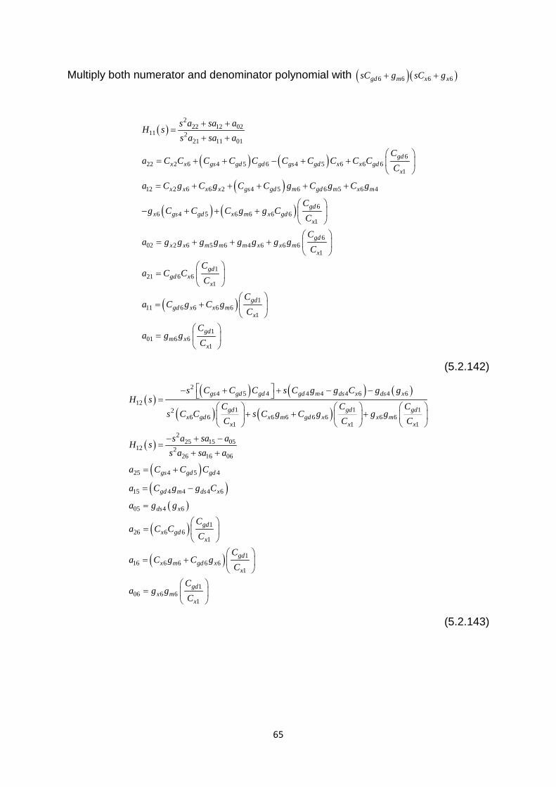
65
Multiply both numerator and denominator polynomial with ( )( )6 6 6 6gd m x xsC g sC g+ +
( )
( ) ( )
( )
( ) ( )
222 12 02
11 221 11 01
622 2 6 4 5 6 4 5 6 6 6
1
12 2 6 6 2 4 5 6 6 5 6 4
66 4 5 6 6 6 6
1
02 2 6 5 6 4
gdx x gs gd gd gs gd x x gd
x
x x x x gs gd m gd m x m
gdx gs gd x m x gd
x
x x m m m x
s a sa aH s
s a sa aC
a C C C C C C C C C CC
a C g C g C C g C g C g
Cg C C C g g C
C
a g g g g g g
+ +=
+ +
= + + − + +
= + + + + +
− + + +
= + +
( )
66 6 6
1
121 6 6
1
111 6 6 6 6
1
101 6 6
1
gdx m
x
gdgd x
x
gdgd x x m
x
gdm x
x
Cg g
C
Ca C C
C
Ca C g C g
C
Ca g g
C
+
=
= +
=
(5.2.142)
( )( ) ( ) ( )
( ) ( )
( )
( )( )
24 5 4 4 4 4 6 4 6
121 1 12
6 6 6 6 6 6 6 61 1 1
225 15 05
12 226 16 06
25 4 5 4
15 4 4 4 6
05 4
gs gd gd gd m ds x ds x
gd gd gdx gd x m gd x x m
x x x
gs gd gd
gd m ds x
ds
s C C C s C g g C g gH s
C C Cs C C s C g C g g g
C C C
s a sa aH s
s a sa a
a C C C
a C g g C
a g g
− + + − − =
+ + +
− + −=
+ +
= +
= −
= ( )
( )
( )
6
126 6 6
1
116 6 6 6 6
1
106 6 6
1
x
gdx gd
x
gdx m gd x
x
gdx m
x
Ca C C
C
Ca C g C g
C
Ca g g
C
=
= +
=
(5.2.143)
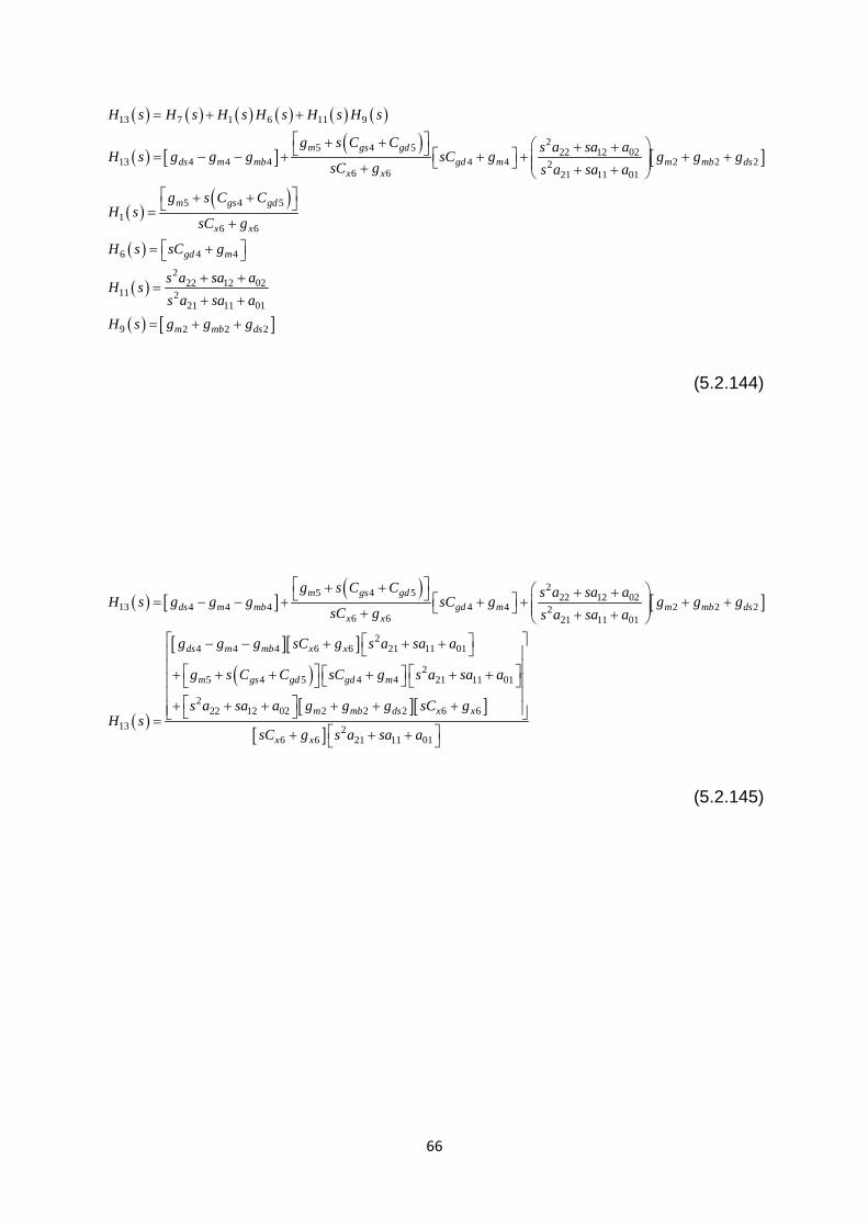
66
( ) ( ) ( ) ( ) ( ) ( )
( ) [ ]( )
[ ]
( )( )
( )
( )
13 7 1 6 11 9
25 4 5 22 12 0213 4 4 4 4 4 2 2 22
6 6 21 11 01
5 4 51
6 6
6 4 4
222 12 02
11 2
m gs gdds m mb gd m m mb ds
x x
m gs gd
x x
gd m
H s H s H s H s H s H s
g s C C s a sa aH s g g g sC g g g g
sC g s a sa a
g s C CH s
sC g
H s sC g
s a sa aH s
s a
= + +
+ + + + = − − + + + + + + + + + + =
+
= +
+ +=
( ) [ ]21 11 01
9 2 2 2m mb ds
sa aH s g g g
+ +
= + +
(5.2.144)
( ) [ ]( )
[ ]
( )
[ ][ ]
( )
25 4 5 22 12 0213 4 4 4 4 4 2 2 22
6 6 21 11 01
24 4 4 6 6 21 11 01
25 4 5 4 4 21 11 01
13
m gs gdds m mb gd m m mb ds
x x
ds m mb x x
m gs gd gd m
g s C C s a sa aH s g g g sC g g g g
sC g s a sa a
g g g sC g s a sa a
g s C C sC g s a sa a
H s
+ + + + = − − + + + + + + + +
− − + + + + + + + + +
=[ ][ ]
[ ]
222 12 02 2 2 2 6 6
26 6 21 11 01
m mb ds x x
x x
s a sa a g g g sC g
sC g s a sa a
+ + + + + +
+ + +
(5.2.145)
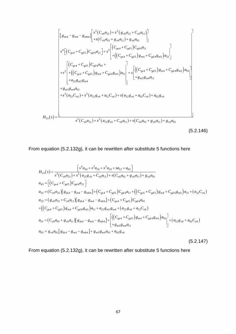
67
( )
[ ] ( ) ( )( )
( )( )
( )( )( )
( )( )
3 26 21 6 21 6 11
4 4 46 01 6 11 6 01
4 5 4 114 34 5 4 21
4 5 4 4 5 21
4 5 4 01
24 5 4 4 5 11
21 5 4
13
x x xds m mb
x x x
gs gd gdgs gd gd
gs gd m gd m
gs gd gd
gs gd m gd m
m m
s C a s g a C ag g g
s C a g a g a
C C C as C C C a s
C C g C g a
C C C a
s C C g C g a
a g g
H s
+ +− −
+ + + + + + + + +
+ +
+ + + +
+
=
( )( )
( ) ( ) ( )
( ) ( ) ( )
4 5 4 4 5 01
5 4 11
5 4 013 2
22 6 22 6 12 6 12 6 02 6 02 6
3 26 21 21 6 6 11 6 01 6 11
gs gd m gd m
m m
m m
x x x x x x
x x x x x
C C g C g as
g g a
g g a
s a C s a g a C s a g a C a g
s C a s a g C a s C a g a
+ + + + + + + + + + +
+ + + + 6 01xg a+
(5.2.146)
From equation (5.2.132g), it can be rewritten after substitute 5 functions here
( )( ) ( ) ( )
( )( )[ ] ( ) ( )( ) ( )
( )
4 3 243 33 23 13 03
13 3 26 21 21 6 6 11 6 01 6 11 6 01
43 4 5 4 21
33 6 21 4 4 4 4 5 4 11 4 5 4 4 5 21 22 6
23 6 21 6 11 4
x x x x x x
gs gd gd
x ds m mb gs gd gd gs gd m gd m x
x x ds m
s a s a s a sa aH s
s C a s a g C a s C a g a g a
a C C C a
a C a g g g C C C a C C g C g a a C
a g a C a g g
+ + + + =+ + + + +
= +
= − − + + + + + +
= + −[ ] ( )( )( ) ( )
( )[ ] ( )( ) ( )
[ ]
4 4 4 5 4 01
4 5 4 4 5 11 21 5 4 22 6 12 6
4 5 4 4 5 0113 6 01 6 11 4 4 4 12 6 02 6
5 4 11
03 6 01 4 4 4 5 4 01 02 6
mb gs gd gd
gs gd m gd m m m x x
gs gd m gd mx x ds m mb x x
m m
x ds m mb m m x
g C C C a
C C g C g a a g g a g a C
C C g C g aa C a g a g g g a g a C
g g a
a g a g g g g g a a g
− + +
+ + + + + +
+ + = + − − + + + +
= − − + +
(5.2.147)
From equation (5.2.132g), it can be rewritten after substitute 5 functions here

68
( ) ( ) ( ) ( ) ( ) ( )
( ) ( ) ( ) ( )
( )
( )( )( )( )( )( )( )
14 6 2 6 12 9
24 25 15 05
14 5 3 4 4 2 2 226 6 26 16 06
25 3 6 6 26 16 06
24 4 26 16 06
225 15 05 2
14
gdx x gd m m mb ds
x x
x x x x
gd gd m
m
H s H s H s H s H s H s
sC s a sa aH s sC g sC g g g g
sC g s a sa a
sC g sC g s a sa a
sC sC g s a sa a
s a sa a g gH s
= − −
− + += + − + − + + + + +
+ + + +
− + + +
− − + + +=
( )( )
( )( )2 2 6 6
26 6 26 16 06
mb ds x x
x x
g sC g
sC g s a sa a
+ + + + +
(5.2.148)
( )
( )( )( )
( ) ( )( )
( )
( )( )( )
25 3 6 6 26 16 06
5 6 065 6 164 3 2
5 6 26 26 3 63 6 26
5 6 3 6 16
5 6 3 6 16 3 6 16 3 6 06
24 4 4 26 16 06
24
14
x x x x
x xx x
x x x xx x
x x x x
x x x x x x x x
gd gd m
gd
sC g sC g s a sa a
C C aC C a
s C C a s s a g gg C a
C g g C a
s C g g C a g g a g g a
sC sC g s a sa a
s C
H s
+ + + +
+ + + + + + + + +
− + + +
−
=
( )( )
( )( )( )
( )( )( )
2 24 4 26 16 06
4 2 3 24 26 4 16 4 4 26
2 24 06 4 4 16 4 4 06
225 15 05 2 2 2 6 6
325 6 2 2 2
225 6 15 6 2 2
gd m
gd gd gd m
gd gd m gd m
m mb ds x x
x m mb ds
x x m mb
sC g s a sa a
s C a s C a C g a
s C a C g a s C g a
s a sa a g g g sC g
s a C g g g
s a g a C g g g
+ + +
+ + − + + +
− − + + + + +
− + +
+ − + + +−
( )( )( )
( )( )( )
2
15 6 05 6 2 2 2
05 6 2 2 2
26 6 26 16 06
ds
x x m mb ds
x m mb ds
x x
s a g a C g g g
a g g g g
sC g s a sa a
+ + + + + + +
+ + +
(5.2.149)
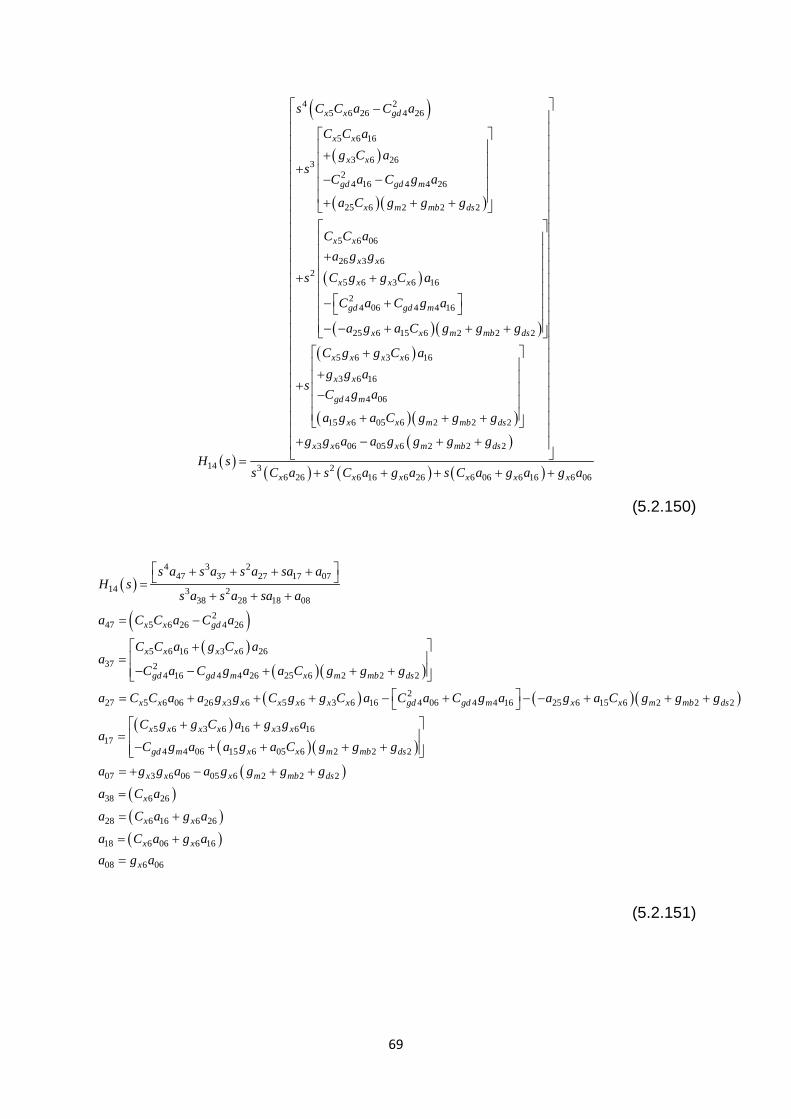
69
( )
( )
( )
( )( )
( )
( )( )
4 25 6 26 4 26
5 6 16
3 6 2632
4 16 4 4 26
25 6 2 2 2
5 6 06
26 3 62
5 6 3 6 16
24 06 4 4 16
25 6 15 6 2 2 2
14
x x gd
x x
x x
gd gd m
x m mb ds
x x
x x
x x x x
gd gd m
x x m mb ds
s C C a C a
C C ag C a
sC a C g a
a C g g g
C C aa g g
s C g g C a
C a C g a
a g a C g g g
H s
−
+
+ − − + + + ++ +
− + − − + + +
=
( )
( )( )( )
( )
5 6 3 6 16
3 6 16
4 4 06
15 6 05 6 2 2 2
3 6 06 05 6 2 2 2
3 26 26 6 16 6
x x x x
x x
gd m
x x m mb ds
x x x m mb ds
x x x
C g g C ag g a
sC g a
a g a C g g g
g g a a g g g g
s C a s C a g a
+ + + − + + +
+ − + +
+ +( ) ( )26 6 06 6 16 6 06x x xs C a g a g a+ + +
(5.2.150)
( )
( )( )
( )( )
( )
4 3 247 37 27 17 07
14 3 238 28 18 08
247 5 6 26 4 26
5 6 16 3 6 2637 2
4 16 4 4 26 25 6 2 2 2
227 5 6 06 26 3 6 5 6 3 6 16 4 06
x x gd
x x x x
gd gd m x m mb ds
x x x x x x x x gd g
s a s a s a sa aH s
s a s a sa a
a C C a C a
C C a g C aa
C a C g a a C g g g
a C C a a g g C g g C a C a C
+ + + + =+ + +
= −
+ =− − + + +
= + + + − + ( )( )( )
( )( )( )
( )( )( )
4 4 16 25 6 15 6 2 2 2
5 6 3 6 16 3 6 1617
4 4 06 15 6 05 6 2 2 2
07 3 6 06 05 6 2 2 2
38 6 26
28 6 16 6 26
18 6 06 6 16
08
d m x x m mb ds
x x x x x x
gd m x x m mb ds
x x x m mb ds
x
x x
x x
x
g a a g a C g g g
C g g C a g g aa
C g a a g a C g g g
a g g a a g g g g
a C a
a C a g a
a C a g aa g
− − + + + + +
= − + + + +
= + − + +
=
= +
= +
= 6 06a
(5.2.151)
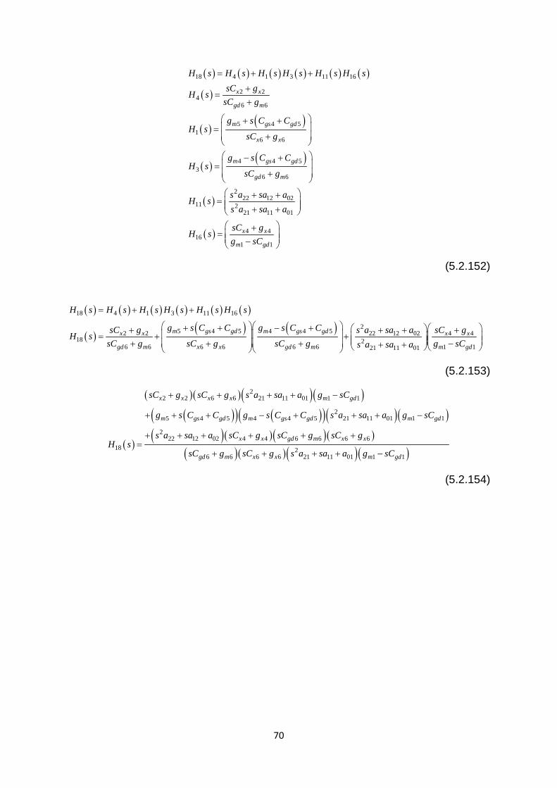
70
( ) ( ) ( ) ( ) ( ) ( )
( )
( )( )
( )( )
( )
( )
18 4 1 3 11 16
2 24
6 6
5 4 51
6 6
4 4 53
6 6
222 12 02
11 221 11 01
4 416
1 1
x x
gd m
m gs gd
x x
m gs gd
gd m
x x
m gd
H s H s H s H s H s H ssC g
H ssC g
g s C CH s
sC g
g s C CH s
sC g
s a sa aH s
s a sa a
sC gH s
g sC
= + +
+=
+
+ + = + − + = + + +
= + + +
= −
(5.2.152)
( ) ( ) ( ) ( ) ( ) ( )
( )( ) ( )
18 4 1 3 11 16
25 4 5 4 4 52 2 22 12 02 4 4
18 26 6 6 6 6 6 1 121 11 01
m gs gd m gs gdx x x x
gd m x x gd m m gd
H s H s H s H s H s H s
g s C C g s C CsC g s a sa a sC gH s
sC g sC g sC g g sCs a sa a
= + +
+ + − + + + + + = + + + + + −+ +
(5.2.153)
( )
( )( )( )( )( )( ) ( )( )( )( )
( )( )( )( )
( )( )( )( )
22 2 6 6 21 11 01 1 1
25 4 5 4 4 5 21 11 01 1 1
222 12 02 4 4 6 6 6 6
18 26 6 6 6 21 11 01 1 1
x x x x m gd
m gs gd m gs gd m gd
x x gd m x x
gd m x x m gd
sC g sC g s a sa a g sC
g s C C g s C C s a sa a g sC
s a sa a sC g sC g sC gH s
sC g sC g s a sa a g sC
+ + + + −
+ + + − + + + −
+ + + + + +=
+ + + + −
(5.2.154)
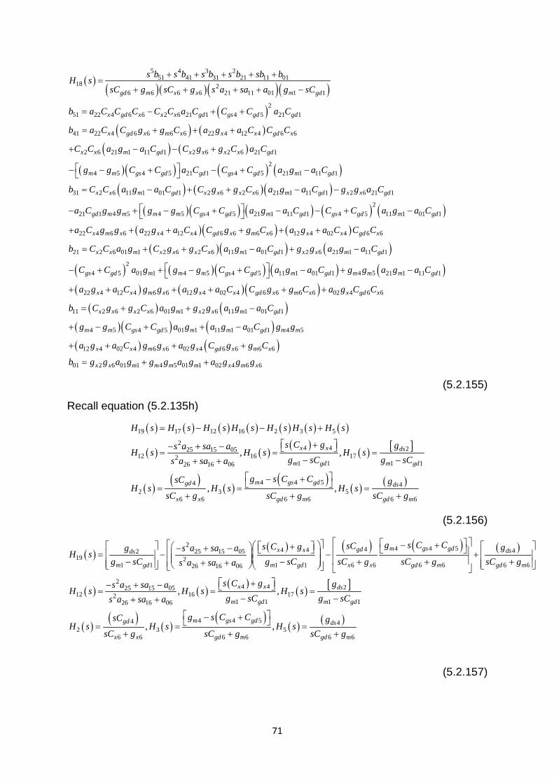
71
( )( )( )( )( )
( )( ) ( )
( )
5 4 3 251 41 31 21 11 01
18 26 6 6 6 21 11 01 1 1
251 22 4 6 6 2 6 21 1 4 5 21 1
41 22 4 6 6 6 6 22 4 12 4 6 6
2 6 21 1 11 1 2 6
gd m x x m gd
x gd x x x gd gs gd gd
x gd x m x x x gd x
x x m gd x x
s b s b s b s b sb bH s
sC g sC g s a sa a g sC
b a C C C C C a C C C a C
b a C C g g C a g a C C C
C C a g a C C g
+ + + + +=
+ + + + −
= − + +
= + + +
+ − − +( )
( )( ) ( ) ( )( ) ( )( )
( )( ) ( ) ( )
2 6 21 1
24 5 4 5 21 1 4 5 21 1 11 1
31 2 6 11 1 01 1 2 6 2 6 21 1 11 1 2 6 21 1
221 1 4 5 4 5 4 5 21 1 11 1 4 5 11 1
x x gd
m m gs gd gd gs gd m gd
x x m gd x x x x m gd x x gd
gd m m m m gs gd m gd gs gd m
g C a C
g g C C a C C C a g a C
b C C a g a C C g g C a g a C g g a C
a C g g g g C C a g a C C C a g a
− − + − + −
= − + + − −
− + − + − − + − ( )( )( ) ( )
( )( ) ( )( ) ( )( ) ( )
01 1
22 4 6 6 22 4 12 4 6 6 6 6 12 4 02 4 6 6
21 2 6 01 1 2 6 2 6 11 1 01 1 2 6 21 1 11 1
24 5 01 1 4 5 4 5 11 1 01 1 4 5 21 1
gd
x m x x x gd x m x x x gd x
x x m x x x x m gd x x m gd
gs gd m m m gs gd m gd m m m
C
a C g g a g a C C g g C a g a C C C
b C C a g C g g C a g a C g g a g a C
C C a g g g C C a g a C g g a g a
+ + + + + +
= + + − + −
− + + − + − + − ( )( ) ( )( )
( ) ( )( )( ) ( )( ) ( )
11 1
22 4 12 4 6 6 12 4 02 4 6 6 6 6 02 4 6 6
11 2 6 2 6 01 1 2 6 11 1 01 1
4 5 4 5 01 1 11 1 01 1 4 5
12 4 02 4 6 6 02 4 6 6 6 6
01
gd
x x m x x x gd x m x x gd x
x x x x m x x m gd
m m gs gd m m gd m m
x x m x x gd x m x
C
a g a C g g a g a C C g g C a g C C
b C g g C a g g g a g a C
g g C C a g a g a C g g
a g a C g g a g C g g C
b
+ + + + + +
= + + −
+ − + + −
+ + + +
2 6 01 1 4 5 01 1 02 4 6 6x x m m m m x m xg g a g g g a g a g g g= + +
(5.2.155)
Recall equation (5.2.135h)
( ) ( ) ( ) ( ) ( ) ( ) ( )
( ) ( )( )
( ) [ ]
( )( )
( )( )
( ) ( )
19 17 12 16 2 3 5
24 4 225 15 05
12 16 1721 1 1 126 16 06
4 4 54 42 3 5
6 6 6 6 6 6
, ,
, ,
x x ds
m gd m gd
m gs gdgd ds
x x gd m gd m
H s H s H s H s H s H s H s
s C g gs a sa aH s H s H s
g sC g sCs a sa a
g s C CsC gH s H s H s
sC g sC g sC g
= − − +
+− + − = = =− −+ +
− + = = =+ + +
(5.2.156)
( )( ) ( ) ( ) ( )
( )
2 4 4 544 4 42 25 15 0519 2
1 1 1 1 6 6 6 6 6 626 16 06
225 15 05
12 226
− + + − + − = − − + − − + + ++ +
− + −=
+
m gs gdgdx x dsds
m gd m gd x x gd m gd m
g s C CsCs C g gg s a sa aH s
g sC g sC sC g sC g sC gs a sa a
s a sa aH s
s a sa( )
( )( ) [ ]
( )( )
( )( )
( ) ( )
4 4 216 17
1 1 1 116 06
4 4 54 42 3 5
6 6 6 6 6 6
, ,
, ,
+ = =− −+
− + = = =+ + +
x x ds
m gd m gd
m gs gdgd ds
x x gd m gd m
s C g gH s H s
g sC g sCa
g s C CsC gH s H s H s
sC g sC g sC g
(5.2.157)
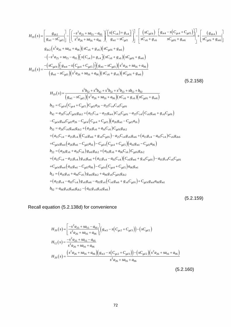
72
( ) ( )( ) ( )
( )
( )( ) ( )( ) ( )( )
225 15 05
20 3 2 3 2226 16 06
225 15 05
12 226 16 06
2 226 16 06 3 2 3 2 26 16 06
20 226 16 06
− + −= − + −
+ +
− + −=
+ +
+ + − + − + +=
+ +
m gs gd gd
m gs gd gd
s a sa aH s g s C C sC
s a sa a
s a sa aH s
s a sa a
s a sa a g s C C sC s a sa aH s
s a sa a
( )( ) ( ) ( ) ( )
( )
( )
2 4 4 544 4 42 25 15 0519 2
1 1 1 1 6 6 6 6 6 626 16 06
22 26 16 06 6
19
− + + − + − = − − + − − + + ++ +
+ + +
=
m gs gdgdx x dsds
m gd m gd x x gd m gd m
ds x
g s C CsCs C g gg s a sa aH s
g sC g sC sC g sC g sC gs a sa a
g s a sa a sC
H s
( )( )( ) ( ) ( )( )( ) ( ) ( )( )( )( )( )( )
6 6 6
225 15 05 4 4 6 6 6 6
24 4 4 5 1 1 26 16 06
21 1 26 16 06 6 6 6 6
+
− − + − + + +
− − + − + + − + + + +
x gd m
x x x x gd m
gd m gs gd m gd
m gd x x gd m
g sC g
s a sa a s C g sC g sC g
sC g s C C g sC s a sa a
g sC s a sa a sC g sC g
(5.2.158)
( )( )( )( )( )( )
( ) ( )
5 4 3 252 42 32 22 12 02
19 21 1 26 16 06 6 6 6 6
52 4 4 5 1 26 25 4 6 6
42 26 6 6 2 15 4 25 4 6 6 25 4 6 6 6 6
4 4 1 26 4 4
+ + + + +=
− + + + +
= + −
= + − − +
− − +
m gd x x gd m
gd gs gd gd x x gd
x gd ds x m x gd x x m x gd
gd m gd gd gs
s b s b s b s b sb bH s
g sC s a sa a sC g sC g
b C C C C a a C C C
b a C C g a C a g C C a C C g g C
C g C a C C( )( )( )
( )( ) ( )
( ) ( )( )( )
5 26 1 1 16
32 26 6 6 2 26 6 16 6 6 2
15 4 25 4 6 6 6 6 25 4 6 6 15 4 05 4 6 6
4 4 26 1 1 16 4 4 5 16 1 1 06
22 26 6 16 6 6 2 16 6
−
= + +
+ − + − + −
+ − − + −
= + +
gd m gd
x m ds x x gd ds
x x x m x gd x x m x x x ds
gd m m gd gd gs gd m gd
x x m ds x
C a g C a
b a C g g a g a C C g
a C a g C g g C a C g g a g a C C g
C g a g C a C C C a g C a
b a g a C g g a g( )( ) ( )( )
( ) ( )( )
( ) ( )
06 6 6 2
15 4 25 4 6 6 15 4 05 4 6 6 6 6 05 4 6 6
4 4 16 1 1 06 4 4 5 06 1
12 16 6 06 6 6 2 06 6 6 2
15 4 05 4 6 6 05 4 6 6 6 6
+
+ − + − + −
+ − − +
= + +
+ − − + +
x gd ds
x x x m x x x m x gd x x gd
gd m m gd gd gs gd m
x x m ds x gd ds
x x x m x x m x gd
a C C g
a C a g g g a g a C C g g C a g C C
C g a g C a C C C a g
b a g a C g g a g C g
a g a C g g a g C g g C
( )4 4 06 1
02 06 6 6 2 05 4 6 6= −
gd m m
x m ds x x m
C g a g
b a g g g a g g g
(5.2.159)
Recall equation (5.2.138d) for convenience
(5.2.160)
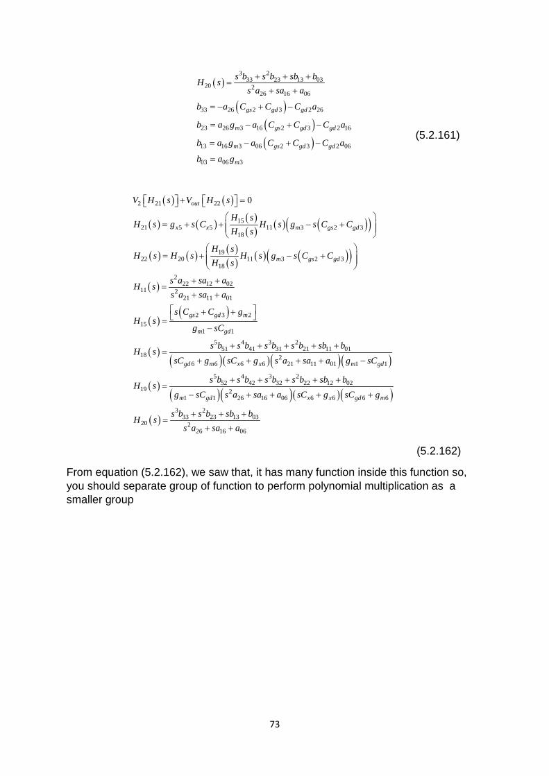
73
( )
( )( )( )
3 233 23 13 03
20 226 16 06
33 26 2 3 2 26
23 26 3 16 2 3 2 16
13 16 3 06 2 3 2 06
03 06 3
+ + +=
+ +
= − + −
= − + −
= − + −
=
gs gd gd
m gs gd gd
m gs gd gd
m
s b s b sb bH s
s a sa a
b a C C C a
b a g a C C C a
b a g a C C C a
b a g
(5.2.161)
( ) ( )
( ) ( ) ( )( ) ( ) ( )( )
( ) ( ) ( )( ) ( ) ( )( )
( )
( )( )
( )
2 21 22
1521 5 5 11 3 2 3
18
1922 20 11 3 2 3
18
222 12 02
11 221 11 01
2 3 215
1 1
5 451 41
18
0+ =
= + + − +
= + − +
+ +=
+ +
+ + =−
+ +=
out
x x m gs gd
m gs gd
gs gd m
m gd
V H s V H s
H sH s g s C H s g s C C
H s
H sH s H s H s g s C C
H s
s a sa aH s
s a sa a
s C C gH s
g sC
s b s b sH s
( )( )( )( )
( )( )( )( )( )
( )
3 231 21 11 01
26 6 6 6 21 11 01 1 1
5 4 3 252 42 32 22 12 02
19 21 1 26 16 06 6 6 6 6
3 233 23 13 03
20 226 16 06
+ + +
+ + + + −
+ + + + +=
− + + + +
+ + +=
+ +
gd m x x m gd
m gd x x gd m
b s b sb bsC g sC g s a sa a g sC
s b s b s b s b sb bH s
g sC s a sa a sC g sC g
s b s b sb bH s
s a sa a
(5.2.162)
From equation (5.2.162), we saw that, it has many function inside this function so, you should separate group of function to perform polynomial multiplication as a smaller group
74
( ) ( )( )
( ) ( )( )( )( )
( ) ( )( ) ( ) ( )
22 6 6 6 6 21 11 01 1 12 3 215 11 22 12 022 5 4 3 2
18 1 121 11 01 51 41 31 21 11 01
15 11 222 12 02 2 3
18
+ + + + −+ + + + = −+ + + + + + +
= + + + +
gd m x x m gdgs gd m
m gd
gs gd m
sC g sC g s a sa a g sCs C C gH s H s s a sa aH s g sCs a sa a s b s b s b s b sb b
H s H ss a sa a s C C g
H s ( ) ( )( )6 6 6 62 5 4 3 2
51 41 31 21 11 01
+ + + + + + +
gd m x xsC g sC g
s b s b s b s b sb b
(5.2.163)
( ) ( )( ) ( ) ( )( )
( )( )( )
6 6 6 615 11 3 234 24 14 04 5 4 3 2
18 51 41 31 21 11 01
34 22 2 3
24 22 2 12 2 3
14 12 2 02 2 3
04 02 2
+ + = + + + + + + + +
= +
= + +
= + +
=
gd m x x
gs gd
m gs gd
m gs gd
m
sC g sC gH s H ss b s b sb b
H s s b s b s b s b sb b
b a C C
b a g a C C
b a g a C C
b a g
(5.2.164)
( ) ( )( ) ( )( ) ( ) ( )( ) ( )( )
( ) ( )( ) ( )( ) ( )( )
6 6 6 615 11 3 23 2 3 34 24 14 04 3 2 35 4 3 2
18 51 41 31 21 11 01
3 2 3 234 24 14 04 35 25 15 0515 11
3 2 3 5 4 318 51 41
+ + − + = + + + − + + + + + +
+ + + + + +− + =
+ +
gd m x xm gs gd m gs gd
m gs gd
sC g sC gH s H sg s C C s b s b sb b g s C C
H s s b s b s b s b sb b
s b s b sb b s b s b sb bH s H sg s C C
H s s b s b s b
( )( )( )
( ) ( )
231 21 11 01
35 6 6 2 3
25 6 6 3 6 6 6 6 2 3
15 6 6 6 6 3 6 6 2 3
05 6 6 3
+ + +
= − +
= − + +
= + − +
=
gd x gs gd
gd x m gd x x m gs gd
gd x x m m m x gs gd
m x m
s b sb b
b C C C C
b C C g C g C g C C
b C g C g g g g C C
b g g g
(5.2.165)
( ) ( )( ) ( )( ) ( )( )3 2 3 2
34 24 14 04 35 25 15 0515 113 2 3 5 4 3 2
18 51 41 31 21 11 01
+ + + + + +− + =
+ + + + +m gs gd
s b s b sb b s b s b sb bH s H sg s C C
H s s b s b s b s b sb b
(5.2.166)
( )( )3 2 3 2 6 5 4 3 234 24 14 04 35 25 15 05 66 56 46 36 26 16 065 4 3 2 5 4 3 2
51 41 31 21 11 01 51 41 31 21 11 01
66 34 35
56 34 25 24 35
46 34 15 24 25 14 35
36 3
+ + + + + + + + + + + +=
+ + + + + + + + + +
=
= +
= + +
=
s b s b sb b s b s b sb b s b s b s b s b s b sb bs b s b s b s b sb b s b s b s b s b sb b
b b bb b b b bb b b b b b bb b 4 05 24 15 14 25 04 35
26 24 05 14 15 04 25
16 14 05 04 15
06 04 05
+ + +
= + +
= +
=
b b b b b b bb b b b b b bb b b b bb b b
(5.2.167)
75
( )
( ) ( ) ( )( ) ( )( ) ( )
6 5 45 51 66 51 5 41 5 56 41 5 31 5 46
3 231 5 21 5 36 21 5 11 5 26
11 5 01 5 16 01 5 0621 5 4 3 2
51 41 31 21 11 01
+ + + + + + +
+ + + + + +
+ + + + +=
+ + + + +
x x x x x
x x x x
x x x
s C b b s b g b C b s b g b C b
s b g b C b s b g b C b
s b g b C b b g bH s
s b s b s b s b sb b
(5.2.168)
( )
( )( )( )( )( )( )
6 5 4 3 267 57 47 37 27 17 07
21 5 4 3 251 41 31 21 11 01
67 5 51 66
57 51 5 41 5 56
47 41 5 31 5 46
37 31 5 21 5 36
27 21 5 11 5 26
17 11 5 01 5 16
07 0
+ + + + + +=
+ + + + +
= +
= + +
= + +
= + +
= + +
= + +
=
x
x x
x x
x x
x x
x x
s b s b s b s b s b sb bH s
s b s b s b s b sb bb C b b
b b g b C b
b b g b C b
b b g b C b
b b g b C b
b b g b C b
b b( )1 5 06+xg b
(5.2.169)
The last intermediate transfer function is recalled here
( ) ( ) ( )( ) ( ) ( )( )
( )
( )( )( )( )( )
( )( )
1922 20 11 3 2 3
18
222 12 02
11 221 11 01
5 4 3 251 41 31 21 11 01
18 26 6 6 6 21 11 01 1 1
5 4 3 252 42 32 22 12 02
191 1
= + − +
+ +=
+ +
+ + + + +=
+ + + + −
+ + + + +=
−
m gs gd
gd m x x m gd
m gd
H sH s H s H s g s C C
H s
s a sa aH s
s a sa a
s b s b s b s b sb bH s
sC g sC g s a sa a g sC
s b s b s b s b sb bH s
g sC ( )( )( )
( )
226 16 06 6 6 6 6
3 233 23 13 03
20 226 16 06
+ + + +
+ + +=
+ +
x x gd ms a sa a sC g sC g
s b s b sb bH s
s a sa a
(5.2.170)
( )( ) ( ) ( )( )
( )( )( )( )( )( )( )( )
1911 3 2 3
18
25 4 3 2 26 6 6 6 21 11 01 1 152 42 32 22 12 02 22 12 025 4 3 2 22
51 41 31 21 11 01 21 1 26 16 06 6 6 6 6
− + =
+ + + + −+ + + + + + += × ×
+ + + + +− + + + +
m gs gd
gd m x x m gd
m gd x x gd m
H sH s g s C C
H s
sC g sC g s a sa a g sCs b s b s b s b sb b s a sa as b s b s b s b sb b s ag sC s a sa a sC g sC g
( )( )
( ) ( )( )
3 2 31 11 01
5 4 3 2 252 42 32 22 12 02 22 12 02
3 2 35 4 3 2251 41 31 21 11 0126 16 06
11
× − ++ +
+ + + + + + += × × × − +
+ + + + ++ +
m gs gd
m gs gd
g s C Csa a
s b s b s b s b sb b s a sa a g s C Cs b s b s b s b sb bs a sa a
(5.2.171)
76
( )( ) ( ) ( )( )
( ) ( )( )
( )
1911 3 2 3
18
5 4 3 2 252 42 32 22 12 02 22 12 02
3 2 35 4 3 2251 41 31 21 11 0126 16 06
7 6 5 4 3 278 68 58 48 38 28 18 08 3 2
− + =
+ + + + + + += × × − +
+ + + + ++ +
+ + + + + + + × − +=
m gs gd
m gs gd
m gs
H sH s g s C C
H s
s b s b s b s b sb b s a sa ag s C C
s b s b s b s b sb bs a sa a
s b s b s b s b s b s b sb b g s C( )( )( )( )
3
2 5 4 3 226 16 06 51 41 31 21 11 01
78 52 22
68 52 12 42 22
58 52 02 42 12 32 22
48 42 02 32 12 22 22
38 32 02 22 12 12 22
28 22 02 12 12 02 22
18 12 02 02 12
08 02 02
+ + + + + + +
=
= +
= + +
= + +
= + +
= + +
= +
=
gdC
s a sa a s b s b s b s b sb b
b b ab b a b ab b a b a b ab b a b a b ab b a b a b ab b a b a b ab b a b ab b a
(5.2.172)
Numerator polynomial have another bracket for multiplication. Its result can be written below
( )( ) ( ) ( )( )
( )( )( )
( )( )( )
1911 3 2 3
18
8 7 6 5 4 3 289 79 69 59 49 39 29 19 09
2 5 4 3 226 16 06 51 41 31 21 11 01
89 78 2 3
79 78 3 68 2 3
69 68 3 58 2 3
59
− + =
+ + + + + + + +=
+ + + + + + +
= − +
= − +
= − +
=
m gs gd
gs gd
m gs gd
m gs gd
H sH s g s C C
H s
s b s b s b s b s b s b s b sb b
s a sa a s b s b s b s b sb b
b b C C
b b g b C C
b b g b C C
b b ( )( )( )( )( )
58 3 48 2 3
49 48 3 38 2 3
39 38 3 28 2 3
29 28 3 18 2 3
19 18 3 08 2 3
09 08 3
− +
= − +
= − +
= − +
= − +
=
m gs gd
m gs gd
m gs gd
m gs gd
m gs gd
m
g b C C
b b g b C C
b b g b C C
b b g b C C
b b g b C C
b b g
(5.2.173)
77
( )( )( )( )8 7 6 5 4 3 23 2 89 79 69 59 49 39 29 19 0933 23 13 03
22 2 2 5 4 3 226 16 06 26 16 06 51 41 31 21 11 01
+ + + + + + + + + + += + + + + + + + + + +
s b s b s b s b s b s b s b sb bs b s b sb bH s
s a sa a s a sa a s b s b s b s b sb b
(5.2.174)
( )( )( )( )
8 7 6 5 4 3 281 71 61 51 41 31 21 11 01
22 2 5 4 3 226 16 06 51 41 31 21 11 01
81 33 51 89
71 33 41 23 51 79
61 33 31 23 41 13 51 69
51 33 21 23 31 13 41 03 51 59
+ + + + + + + +=
+ + + + + + +
= +
= + +
= + + +
= + + + +
s c s c s c s c s c s c s c sc cH s
s a sa a s b s b s b s b sb b
c b b bc b b b b bc b b b b b b bc b b b b b b b b bc41 33 11 23 21 13 31 03 41 49
31 33 01 23 11 13 21 03 31 39
21 23 01 13 11 03 21 29
11 13 01 03 11 19
01 03 01 09
= + + + +
= + + + +
= + + +
= + +
= +
b b b b b b b b bc b b b b b b b b bc b b b b b b bc b b b b bc b b b
(5.2.175)
Denominator polynomial have another bracket for multiplication. Its result can be written below.
( )( )
( )8 7 6 5 4 3 2
81 71 61 51 41 31 21 11 0122 7 6 5 4 3 2
72 62 52 42 33 22 12 02
72 26 51
62 26 41 16 51
52 26 31 16 41 06 51
42 26 21 16 31 06 41
32 26 11 16 21 06 31
2
+ + + + + + + +=
+ + + + + + +
=
= +
= + +
= + +
= + +
s c s c s c s c s c s c s c sc cH s
s c s c s c s c s c s c sc b
c a bc a b a bc a b a b a bc b b b b b bc b b b b b bc 2 26 01 16 11 06 21
12 16 01 06 11
02 06 01
= + +
= +
=
b b b b b bc b b b bc b b
(5.2.176)
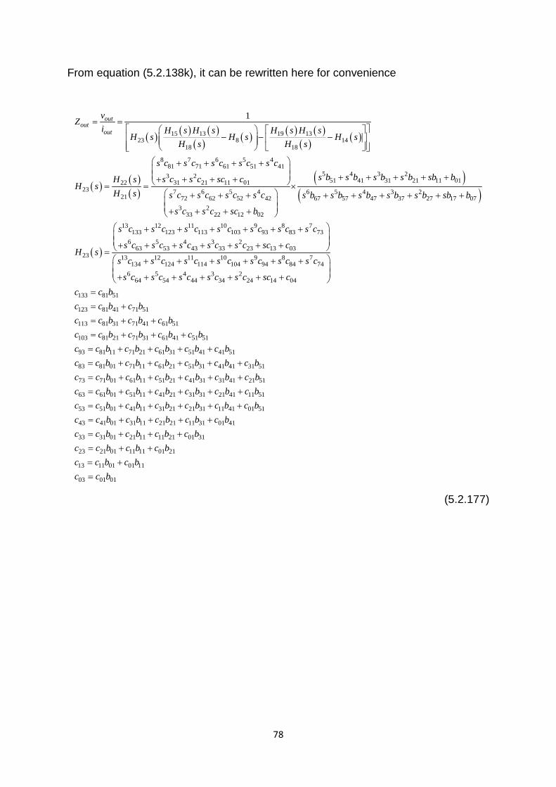
78
From equation (5.2.138k), it can be rewritten here for convenience
( ) ( ) ( )( ) ( ) ( ) ( )
( ) ( )
( ) ( )( )
15 13 19 1323 8 14
18 18
8 7 6 5 481 71 61 51 41
3 231 21 11 0122
23 7 6 5 421 72 62 52 42
3 233 22 12 02
1= =
− − −
+ + + + + + + + = = ×
+ + + + + + +
outout
out
vZ
i H s H s H s H sH s H s H s
H s H s
s c s c s c s c s c
s c s c sc cH sH s
H s s c s c s c s c
s c s c sc b
( )( )
( )
5 4 3 251 41 31 21 11 01
6 5 4 3 267 57 47 37 27 17 07
13 12 11 10 9 8 7133 123 113 103 93 83 73
6 5 4 3 263 53 43 33 23 13 03
23 13 12 11 10134 124 114 1
+ + + + +
+ + + + + +
+ + + + + + + + + + + + + =
+ + +
s b s b s b s b sb b
s b s b s b s b s b sb b
s c s c s c s c s c s c s c
s c s c s c s c s c sc cH s
s c s c s c s c 9 8 704 94 84 74
6 5 4 3 264 54 44 34 24 14 04
133 81 51
123 81 41 71 51
113 81 31 71 41 61 51
103 81 21 71 31 61 41 51 51
93 81 11 71 21 61 31 51 41 41 51
83 81 0
+ + + + + + + + + +
=
= +
= + +
= + + +
= + + + +
=
s c s c s c
s c s c s c s c s c sc cc c bc c b c bc c b c b c bc c b c b c b c bc c b c b c b c b c bc c b 1 71 11 61 21 51 31 41 41 31 51
73 71 01 61 11 51 21 41 31 31 41 21 51
63 61 01 51 11 41 21 31 31 21 41 11 51
53 51 01 41 11 31 21 21 31 11 41 01 51
43 41 01 31 11 21 21 11
+ + + + +
= + + + + +
= + + + + +
= + + + + +
= + + +
c b c b c b c b c bc c b c b c b c b c b c bc c b c b c b c b c b c bc c b c b c b c b c b c bc c b c b c b c b31 01 41
33 31 01 21 11 11 21 01 31
23 21 01 11 11 01 21
13 11 01 01 11
03 01 01
+
= + + +
= + +
= +
=
c bc c b c b c b c bc c b c b c bc c b c bc c b
(5.2.177)
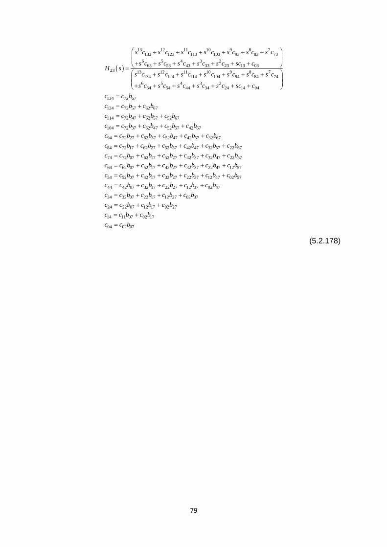
79
( )
13 12 11 10 9 8 7133 123 113 103 93 83 73
6 5 4 3 263 53 43 33 23 13 03
23 13 12 11 10 9 8 7134 124 114 104 94 84 74
6 5 4 3 264 54 44 34 24 14 04
13
+ + + + + + + + + + + + + = + + + + + + + + + + + + +
s c s c s c s c s c s c s c
s c s c s c s c s c sc cH s
s c s c s c s c s c s c s c
s c s c s c s c s c sc cc 4 72 67
124 72 57 62 67
114 72 47 62 57 52 67
104 72 37 62 47 52 57 42 67
94 72 27 62 37 52 47 42 57 32 67
84 72 17 62 27 52 37 42 47 32 57 22 67
74 72 07 62 17 52 27 42 37 3
=
= +
= + +
= + + +
= + + + +
= + + + + +
= + + + +
c bc c b c bc c b c b c bc c b c b c b c bc c b c b c b c b c bc c b c b c b c b c b c bc c b c b c b c b c 2 47 22 57
64 62 07 52 17 42 27 32 37 22 47 12 57
54 52 07 42 17 32 27 22 37 12 47 02 57
44 42 07 32 17 22 27 12 37 02 47
34 32 07 22 17 12 27 02 37
24 22 07 12 17 02 27
14 1
+
= + + + + +
= + + + + +
= + + + +
= + + +
= + +
=
b c bc c b c b c b c b c b c bc c b c b c b c b c b c bc c b c b c b c b c bc c b c b c b c bc c b c b c bc c 1 07 02 17
04 02 07
+
=
b c bc c b
(5.2.178)
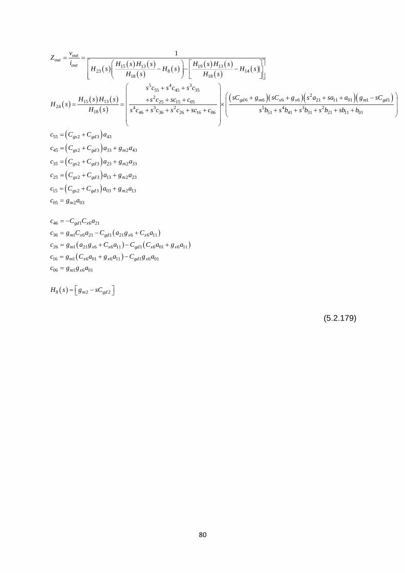
80
( ) ( ) ( )( ) ( ) ( ) ( )
( ) ( )
( ) ( ) ( )( )
( )( )( )
15 13 19 1323 8 14
18 18
5 4 355 45 35
22 6 6 6 6 21 11 01 115 13 25 15 0524 4 3 2
18 46 36 26 16 06
1= =
− − −
+ +
+ + + + + + += = ×
+ + + +
outout
out
gd m x x m
vZ
i H s H s H s H sH s H s H s
H s H s
s c s c s csC g sC g s a sa a gH s H s s c sc c
H sH s s c s c s c sc c
( )
( )( )( )( )( )
15 4 3 2
51 41 31 21 11 01
55 2 3 43
45 2 3 33 2 43
35 2 3 23 2 33
25 2 3 13 2 23
15 2 3 03 2 13
05 2 03
46 1 6 21
36 1 6 21 1 21
− + + + + +
= +
= + +
= + +
= + +
= + +
=
= −
= −
gd
gs gd
gs gd m
gs gd m
gs gd m
gs gd m
m
gd x
m x gd
sC
s b s b s b s b sb b
c C C a
c C C a g a
c C C a g a
c C C a g a
c C C a g a
c g a
c C C a
c g C a C a( )( ) ( )( )
( )
6 6 11
26 1 21 6 6 11 1 6 01 6 11
16 1 6 01 6 11 1 6 01
06 1 6 01
8 2 2
+
= + − +
= + −
=
= −
x x
m x x gd x x
m x x gd x
m x
m gd
g C a
c g a g C a C C a g a
c g C a g a C g a
c g g a
H s g sC
(5.2.179)
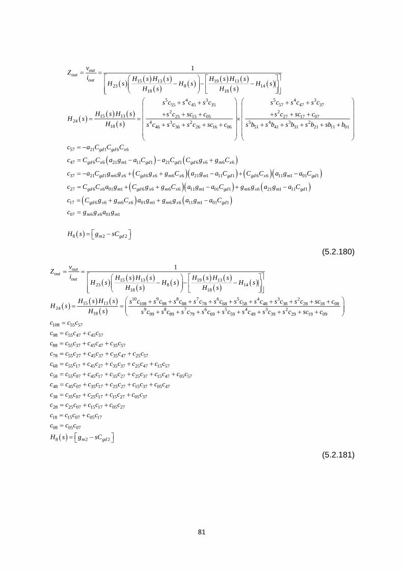
81
( ) ( ) ( )( ) ( ) ( ) ( )
( ) ( )
( ) ( ) ( )( )
15 13 19 1323 8 14
18 18
5 4 3 5 4 355 45 35 57 47 37
2 215 13 25 15 05 27 17 07
24 4 3 2 518 46 36 26 16 06
1= =
− − −
+ + + + + + + + + +
= = × + + + +
outout
out
vZ
i H s H s H s H sH s H s H s
H s H s
s c s c s c s c s c s c
H s H s s c sc c s c sc cH s
H s s c s c s c sc c s
( ) ( )( )( ) ( )( )
4 3 251 41 31 21 11 01
57 21 1 6 6
47 6 6 21 1 11 1 21 1 6 6 6 6
37 21 1 6 6 6 6 6 6 21 1 11 1 6 6 11 1 01 1
27 6 6 01 1
+ + + + +
= −
= − − +
= − + + − + −
= +
gd gd x
gd x m gd gd gd x m x
gd m x gd x m x m gd gd x m gd
gd x m gd
b s b s b s b sb b
c a C C C
c C C a g a C a C C g g C
c a C g g C g g C a g a C C C a g a C
c C C a g C( )( ) ( )( ) ( )
( )
6 6 6 6 11 1 01 1 6 6 21 1 11 1
17 6 6 6 6 01 1 6 6 11 1 01 1
07 6 6 01 1
8 2 2
+ − + −
= + + −
=
= −
x m x m gd m x m gd
gd x m x m m x m gd
m x m
m gd
g g C a g a C g g a g a C
c C g g C a g g g a g a C
c g g a g
H s g sC
(5.2.180)
( ) ( ) ( )( ) ( ) ( ) ( )
( ) ( )
( ) ( ) ( )( )
15 13 19 1323 8 14
18 18
10 9 8 7 6 5 4 3 215 13 108 98 88 78 68 58 48 38 28 18 08
24 9 8 7 6 5 4 318 99 89 79 69 59 49 39
1= =
− − −
+ + + + + + + + + += =
+ + + + + + +
outout
out
vZ
i H s H s H s H sH s H s H s
H s H s
H s H s s c s c s c s c s c s c s c s c s c sc cH s
H s s c s c s c s c s c s c s c s229 19 09
108 55 57
98 55 47 45 57
88 55 37 45 47 35 57
78 55 27 45 37 35 47 25 57
68 55 17 45 27 35 37 25 47 15 57
58 55 07 45 17 35 27 25 37 15 47 05 57
48 45 07 3
+ +
=
= +
= + +
= + + +
= + + + +
= + + + + +
= +
c sc cc c cc c c c cc c c c c c cc c c c c c c c cc c c c c c c c c c cc c c c c c c c c c c c cc c c c
( )
5 17 25 27 15 37 05 47
38 35 07 25 17 15 27 05 37
28 25 07 15 17 05 27
18 15 07 05 17
08 05 07
8 2 2
+ + +
= + + +
= + +
= +
=
= − m gd
c c c c c c cc c c c c c c c cc c c c c c cc c c c cc c c
H s g sC
(5.2.181)
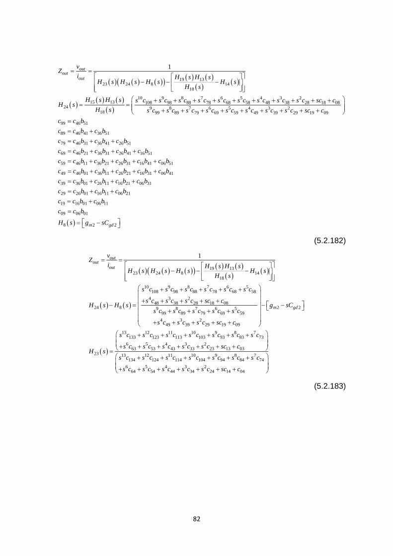
82
( ) ( ) ( )( ) ( ) ( )( ) ( )
( ) ( ) ( )( )
19 1323 24 8 14
18
10 9 8 7 6 5 4 3 215 13 108 98 88 78 68 58 48 38 28 18 08
24 9 8 7 6 5 4 3 218 99 89 79 69 59 49 39 29 19 09
1= =
− − −
+ + + + + + + + + +
= = + + + + + + + + +
outout
out
vZ
i H s H sH s H s H s H s
H s
H s H s s c s c s c s c s c s c s c s c s c sc cH s
H s s c s c s c s c s c s c s c s c sc c
99 46 51
89 46 41 36 51
79 46 31 36 41 26 51
69 46 21 36 31 26 41 16 51
59 46 11 36 21 26 31 16 41 06 51
49 46 01 36 11 26 21 16 31 06 41
39 36 01 26 11 16 21 06 31
29 2
=
= +
= + +
= + + +
= + + + +
= + + + +
= + + +
=
c c bc c b c bc c b c b c bc c b c b c b c bc c b c b c b c b c bc c b c b c b c b c bc c b c b c b c bc c
( )
6 01 16 11 06 21
19 16 01 06 11
09 06 01
8 2 2
+ +
= +
=
= − m gd
b c b c bc c b c bc c b
H s g sC
(5.2.182)
( ) ( ) ( )( ) ( ) ( )( ) ( )
( ) ( )
19 1323 24 8 14
18
10 9 8 7 6 5108 98 88 78 68 58
4 3 248 38 28 18 08
24 8 9 8 7 6 599 89 79 69 59
4 3 249 39 29 19 09
1= =
− − −
+ + + + + + + + + +
− = + + + +
+ + + + +
outout
out
vZ
i H s H sH s H s H s H s
H s
s c s c s c s c s c s c
s c s c s c sc cH s H s
s c s c s c s c s c
s c s c s c sc c
( )
2 2
13 12 11 10 9 8 7133 123 113 103 93 83 73
6 5 4 3 263 53 43 33 23 13 03
23 13 12 11 10 9 8 7134 124 114 104 94 84 74
6 5 4 3 264 54 44 34 24 1
− −
+ + + + + + + + + + + + + =
+ + + + + +
+ + + + + +
m gdg sC
s c s c s c s c s c s c s c
s c s c s c s c s c sc cH s
s c s c s c s c s c s c s c
s c s c s c s c s c sc 4 04
+ c
(5.2.183)
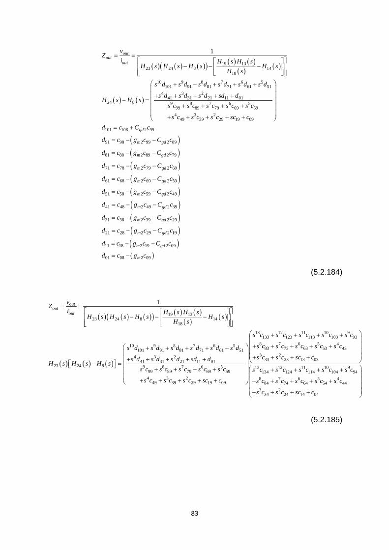
83
( ) ( ) ( )( ) ( ) ( )( ) ( )
( ) ( )
19 1323 24 8 14
18
10 9 8 7 6 5101 91 81 71 61 51
4 3 241 31 21 11 01
24 8 9 8 7 6 599 89 79 69 59
4 3 249 39 29 19 09
1= =
− − −
+ + + + + + + + + +
− = + + + +
+ + + + +
outout
out
vZ
i H s H sH s H s H s H s
H s
s d s d s d s d s d s d
s d s d s d sd dH s H s
s c s c s c s c s c
s c s c s c sc c
( )( )( )( )( )( )( )( )
101 108 2 99
91 98 2 99 2 89
81 88 2 89 2 79
71 78 2 79 2 69
61 68 2 69 2 59
51 58 2 59 2 49
41 48 2 49 2 39
31 38 2 39 2 29
21 28 2 29 2 19
11
= +
= − −
= − −
= − −
= − −
= − −
= − −
= − −
= − −
=
gd
m gd
m gd
m gd
m gd
m gd
m gd
m gd
m gd
d c C c
d c g c C c
d c g c C c
d c g c C c
d c g c C c
d c g c C c
d c g c C c
d c g c C c
d c g c C c
d c ( )( )
18 2 19 2 09
01 08 2 09
− −
= −
m gd
m
g c C c
d c g c
(5.2.184)
( ) ( ) ( )( ) ( ) ( )( ) ( )
( ) ( ) ( )
19 1323 24 8 14
18
10 9 8 7 6 5101 91 81 71 61 51
4 3 241 31 21 11 01
23 24 8 9 8 7 6 599 89 79 69 59
4 3 249 39 29 19 09
1= =
− − −
+ + + + + + + + + +
− = + + + +
+ + + + +
outout
out
vZ
i H s H sH s H s H s H s
H s
s d s d s d s d s d s d
s d s d s d sd dH s H s H s
s c s c s c s c s c
s c s c s c sc c
13 12 11 10 9133 123 113 103 93
8 7 6 5 483 73 63 53 43
3 233 23 13 03
13 12 11 10 9134 124 114 104 94
8 7 6 5 484 74 64 54 44
3 234 24 14 04
+ + + + + + + + + + + + +
+ + + + + + + + +
+ + + +
s c s c s c s c s c
s c s c s c s c s c
s c s c sc c
s c s c s c s c s c
s c s c s c s c s c
s c s c sc c
(5.2.185)
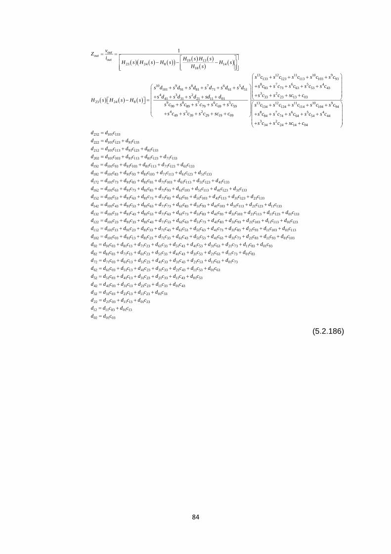
84
( ) ( ) ( )( ) ( ) ( )( ) ( )
( ) ( ) ( )
19 1323 24 8 14
18
10 9 8 7 6 5101 91 81 71 61 51
4 3 241 31 21 11 01
23 24 8 9 8 7 6 599 89 79 69 59
4 3 249 39 29 19 09
1= =
− − −
+ + + + +
+ + + + +− = + + + +
+ + + + +
outout
out
vZi H s H s
H s H s H s H sH s
s d s d s d s d s d s d
s d s d s d sd dH s H s H ss c s c s c s c s c
s c s c s c sc c
13 12 11 10 9133 123 113 103 93
8 7 6 5 483 73 63 53 43
3 233 23 13 03
13 12 11 10 9134 124 114 104 94
8 7 6 5 484 74 64 54 44
3 234 24 14 04
+ + + + + + + + + + + + +
+ + + +
+ + + + +
+ + + +
s c s c s c s c s c
s c s c s c s c s c
s c s c sc c
s c s c s c s c s c
s c s c s c s c s c
s c s c sc c
232 101 133
222 101 123 91 133
212 101 113 91 123 81 133
202 101 103 91 113 81 123 71 133
192 101 93 91 103 81 113 71 123 61 133
182 101 83 91 93 81 103 71 113 61 123
=
= +
= + +
= + + +
= + + + +
= + + + + +
d d cd d c d cd d c d c d cd d c d c d c d cd d c d c d c d c d cd d c d c d c d c d c 51 133
172 101 73 91 83 81 93 71 103 61 113 51 123 41 133
162 101 63 91 73 81 83 71 93 61 103 51 113 41 123 31 133
152 101 53 91 63 81 73 71 83 61 93 51 103 41 113 31 123 21 1
= + + + + + +
= + + + + + + +
= + + + + + + + +
d cd d c d c d c d c d c d c d cd d c d c d c d c d c d c d c d cd d c d c d c d c d c d c d c d c d c 33
142 101 43 91 53 81 63 71 73 61 83 51 93 41 103 31 113 21 123 11 133
132 101 33 91 43 81 53 71 63 61 73 51 83 41 93 31 103 21 113 11 123 01 133
122 101 23 91 33 81 43 71 53
= + + + + + + + + +
= + + + + + + + + + +
= + + +
d d c d c d c d c d c d c d c d c d c d cd d c d c d c d c d c d c d c d c d c d c d cd d c d c d c d c 61 63 51 73 41 83 31 93 21 103 11 113 01 123
112 101 13 91 23 81 33 71 43 61 53 51 63 41 73 31 83 21 93 11 103 01 113
102 101 03 91 13 81 23 71 33 61 43 51 53 41 63 31 73 2
+ + + + + + +
= + + + + + + + + + +
= + + + + + + + +
d c d c d c d c d c d c d cd d c d c d c d c d c d c d c d c d c d c d cd d c d c d c d c d c d c d c d c d 1 83 11 93 01 103
92 91 03 81 13 71 23 61 33 51 43 41 53 31 63 21 73 11 83 01 93
82 81 03 71 13 61 23 51 33 41 43 31 53 21 63 11 73 01 83
72 71 03 61 13 51 23 41 33 31 43 21
+ +
= + + + + + + + + +
= + + + + + + + +
= + + + + +
c d c d cd d c d c d c d c d c d c d c d c d c d cd d c d c d c d c d c d c d c d c d cd d c d c d c d c d c d 53 11 63 01 73
62 61 03 51 13 41 23 31 33 21 43 11 53 01 63
52 51 03 41 13 31 23 21 33 11 43 01 53
42 41 03 31 13 21 23 11 33 01 43
32 31 03 21 13 11 23 01 33
22 21 03 11 13
+ +
= + + + + + +
= + + + + +
= + + + +
= + + +
= +
c d c d cd d c d c d c d c d c d c d cd d c d c d c d c d c d cd d c d c d c d c d cd d c d c d c d cd d c d c 01 23
12 11 03 01 13
02 01 03
+
= +
=
d cd d c d cd d c
(5.2.186)
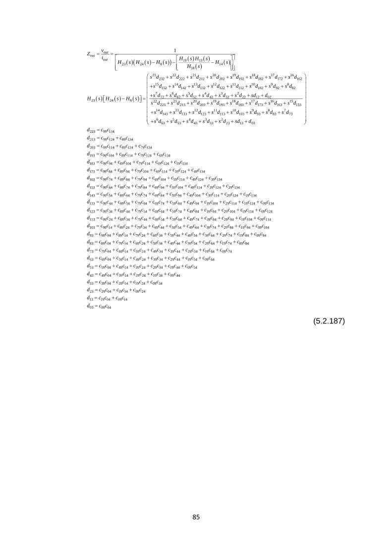
85
( ) ( ) ( )( ) ( ) ( )( ) ( )
( ) ( ) ( )
19 1323 24 8 14
18
23 22 21 20 19 18 17 16232 222 212 202 192 182 172 162
15 14 13 12 11 10 9 8152 142 132 122 112 102 92 8
23 24 8
1= =
− − −
+ + + + + + +
+ + + + + + + +
− =
outout
out
vZi H s H s
H s H s H s H sH s
s d s d s d s d s d s d s d s d
s d s d s d s d s d s d s d s d
H s H s H s
27 6 5 4 3 2
72 62 52 42 32 22 12 0222 21 20 19 18 17 16 15
223 213 203 193 183 173 163 15314 13 12 11 10 9 8 7
143 133 123 113 103 93 83 736 5 4 3 2
63 53 43 33 23
+ + + + + + + ++ + + + + + +
+ + + + + + + +
+ + + + + +
s d s d s d s d s d s d sd ds d s d s d s d s d s d s d s d
s d s d s d s d s d s d s d s d
s d s d s d s d s d sd13 03
223 99 134
213 99 124 89 134
203 99 114 89 124 79 134
193 99 104 89 114 79 124 69 134
183 99 94 89 104 79 114 69 124 59 134
173 99 84 89 94 79 104 69 11
+
=
= +
= + +
= + + +
= + + + +
= + + +
dd c cd c c c cd c c c c c cd c c c c c c c cd c c c c c c c c c cd c c c c c c c c 4 59 124 49 134
163 99 74 89 84 79 94 69 104 59 114 49 124 39 134
153 99 64 89 74 79 84 69 94 59 104 49 114 39 124 29 134
143 99 54 89 64 79 74 69 84 59 94 49 104 39 114 29 12
+ +
= + + + + + +
= + + + + + + +
= + + + + + + +
c c c cd c c c c c c c c c c c c c cd c c c c c c c c c c c c c c c cd c c c c c c c c c c c c c c c c 4 19 134
133 99 44 89 54 79 64 69 74 59 84 49 94 39 104 29 114 19 124 09 134
123 99 34 89 44 79 54 69 64 59 74 49 84 39 94 29 104 19 114 09 124
113 99 24 89 34 79 44 69 54 59
+
= + + + + + + + + +
= + + + + + + + + +
= + + + +
c cd c c c c c c c c c c c c c c c c c c c cd c c c c c c c c c c c c c c c c c c c cd c c c c c c c c c 64 49 74 39 84 29 94 19 104 09 114
103 99 14 89 24 79 34 69 44 59 54 49 64 39 74 29 84 19 94 09 104
93 99 04 89 14 79 24 69 34 59 44 49 54 39 64 29 74 19 84 09 94
83 89 04
+ + + + +
= + + + + + + + + +
= + + + + + + + + +
= +
c c c c c c c c c c cd c c c c c c c c c c c c c c c c c c c cd c c c c c c c c c c c c c c c c c c c cd c c c79 14 69 24 59 34 49 44 39 54 29 64 19 74 09 84
73 79 04 69 14 59 24 49 34 39 44 29 54 19 64 09 74
63 69 04 59 14 49 24 39 34 29 44 19 54 09 64
53 59 04 49 14 39 24 29 34 19
+ + + + + + +
= + + + + + + +
= + + + + + +
= + + + +
c c c c c c c c c c c c c c cd c c c c c c c c c c c c c c c cd c c c c c c c c c c c c c cd c c c c c c c c c 44 09 54
43 49 04 39 14 29 24 19 34 09 44
33 39 04 29 14 19 24 09 34
23 29 04 19 14 09 24
13 19 04 09 14
03 09 04
+
= + + + +
= + + +
= + +
= +
=
c c cd c c c c c c c c c cd c c c c c c c cd c c c c c cd c c c cd c c
(5.2.187)
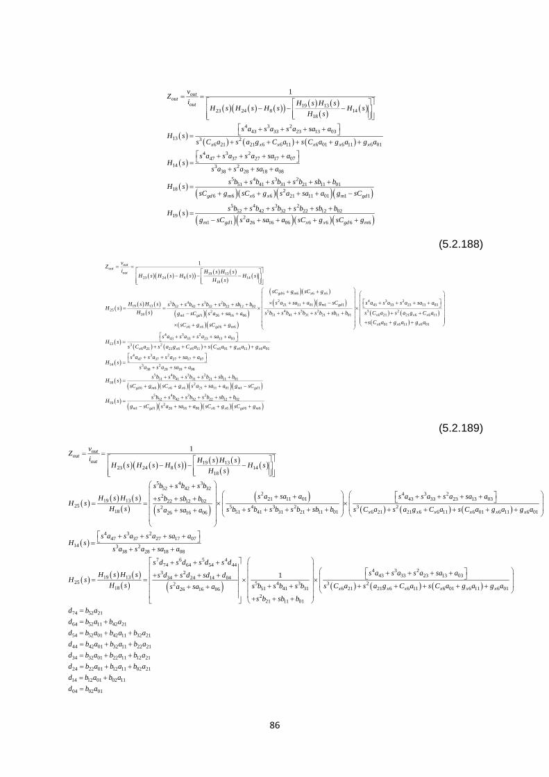
86
( ) ( ) ( )( ) ( ) ( )( ) ( )
( )( ) ( ) ( )
( )
19 1323 24 8 14
18
4 3 243 33 23 13 03
13 3 26 21 21 6 6 11 6 01 6 11 6 01
4 3 247 37 27 17 07
14 3 238 28 18 08
18
1= =
− − −
+ + + + =
+ + + + +
+ + + + =+ + +
outout
out
x x x x x x
vZi H s H s
H s H s H s H sH s
s a s a s a sa aH s
s C a s a g C a s C a g a g a
s a s a s a sa aH s
s a s a sa a
H ( )( )( )( )( )
( )( )( )( )( )
5 4 3 251 41 31 21 11 01
26 6 6 6 21 11 01 1 1
5 4 3 252 42 32 22 12 02
19 21 1 26 16 06 6 6 6 6
+ + + + +=
+ + + + −
+ + + + +=
− + + + +
gd m x x m gd
m gd x x gd m
s b s b s b s b sb bssC g sC g s a sa a g sC
s b s b s b s b sb bH sg sC s a sa a sC g sC g
(5.2.188)
( ) ( ) ( )( ) ( ) ( )( ) ( )
( ) ( ) ( )( ) ( )( )
( )( )
( )( )
( )( )
19 1323 24 8 14
18
6 6 6 6
25 4 3 2 21 11 01 1 119 13 52 42 32 22 12 0225 52
18 511 1 26 16 06
6 6 6 6
1= =
− − −
+ +
× + + −+ + + + += = ×
+− + +
× + +
outout
out
gd m x x
m gd
m gd
x x gd m
vZ
i H s H sH s H s H s H s
H s
sC g sC g
s a sa a g sCH s H s s b s b s b s b sb bH s
H s s bg sC s a sa a
sC g sC g
( ) ( )( )
( )( ) ( )
4 3 243 33 23 13 03
4 3 2 3 241 31 21 11 01 6 21 21 6 6 11
6 01 6 11 6 01
4 3 243 33 23 13 03
13 3 26 21 21 6 6 11
+ + + + × + + + + + + + + + + + + + =
+ + +
x x x
x x x
x x x x
s a s a s a sa a
s b s b s b sb b s C a s a g C a
s C a g a g a
s a s a s a sa aH s
s C a s a g C a s C( )
( )
( )( )( )( )( )
( )( )
6 01 6 11 6 01
4 3 247 37 27 17 07
14 3 238 28 18 08
5 4 3 251 41 31 21 11 01
18 26 6 6 6 21 11 01 1 1
5 4 3 252 42 32 22 12 02
19 21 1 2
+ +
+ + + + =+ + +
+ + + + +=
+ + + + −
+ + + + +=
−
x x
gd m x x m gd
m gd
a g a g a
s a s a s a sa aH s
s a s a sa a
s b s b s b s b sb bH s
sC g sC g s a sa a g sC
s b s b s b s b sb bH s
g sC s a( )( )( )6 16 06 6 6 6 6+ + + +x x gd msa a sC g sC g
(5.2.189)
( ) ( ) ( )( ) ( ) ( )( ) ( )
( ) ( ) ( )( ) ( )
( )
19 1323 24 8 14
18
5 4 352 42 32
2 42 21 11 01 4319 13 22 12 0225 5 4 3 22
18 51 41 31 21 11 0126 16 06
1= =
− − −
+ + + + + + + = = × × + + + + ++ +
outout
out
vZi H s H s
H s H s H s H sH s
s b s b s bs a sa a s aH s H s s b sb bH s
H s s b s b s b s b sb bs a sa a ( ) ( ) ( )
( )
( ) ( ) ( )( )
3 233 23 13 03
3 26 21 21 6 6 11 6 01 6 11 6 01
4 3 247 37 27 17 07
14 3 238 28 18 08
7 6 5 474 64 54 44
3 219 13 34 24 14 04
25 218 2
+ + + + + + + + +
+ + + + =+ + +
+ + +
+ + + += =
x x x x x x
s a s a sa a
s C a s a g C a s C a g a g a
s a s a s a sa aH s
s a s a sa a
s d s d s d s d
H s H s s d s d sd dH sH s s a( ) ( ) ( ) ( )
4 3 243 33 23 13 03
5 4 3 3 251 41 31 6 21 21 6 6 11 6 01 6 11 6 016 16 062
21 11 01
74 52 21
64 52 11 42 21
54 52 01 42 1
1
+ + + + × × + + + + + + ++ + + + +
=
= +
= +
x x x x x x
s a s a s a sa a
s b s b s b s C a s a g C a s C a g a g asa a
s b sb bd b ad b a b ad b a b a 1 32 21
44 42 01 32 11 22 21
34 32 01 22 11 12 21
24 22 01 12 11 02 21
14 12 01 02 11
04 02 01
+
= + +
= + +
= + +
= +
=
b ad b a b a b ad b a b a b ad b a b a b ad b a b ad b a
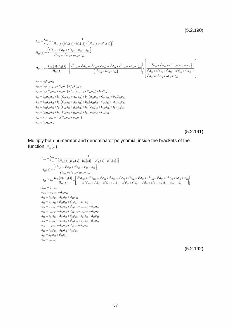
87
(5.2.190)
( ) ( ) ( )( ) ( ) ( )
( )
( ) ( ) ( )( ) ( )
23 24 8 25 14
4 3 247 37 27 17 07
14 3 238 28 18 08
4 3 27 6 5 4 3 2 43 3319 13 74 64 54 44 34 24 14 0425 2
18 26 16 06
1= =
− − − + + + + =
+ + +
+ ++ + + + + + + = = × + +
outout
out
vZi H s H s H s H s H s
s a s a s a sa aH s
s a s a sa a
s a s a s aH s H s s d s d s d s d s d s d sd dH sH s s a sa a
( )( ) ( )
( )
23 13 038 7 6 5 4
85 75 65 55 453 2
35 25 15 05
85 51 6 21
75 51 21 6 6 11 41 6 21
65 51 6 01 6 11 41 21 6 6 11 31 6 21
55 51 6 01 41 6 01 6 11
+ +
+ + + + + + + +
=
= + +
= + + + +
= + + +
x
x x x
x x x x x
x x x
sa a
s d s d s d s d s d
s d s d sd dd b C ad b a g C a b C a
d b C a g a b a g C a b C a
d b g a b C a g a ( )( ) ( )( ) ( )( ) ( )
31 21 6 6 11 21 6 21
45 41 6 01 31 6 01 6 11 21 21 6 6 11 11 6 21
35 31 6 01 21 6 01 6 11 11 21 6 6 11 01 6 21
25 21 6 01 11 6 01 6 11 01 21 6 6 11
15 11 6 01
+ +
= + + + + +
= + + + + +
= + + + +
=
x x x
x x x x x x
x x x x x x
x x x x x
x
b a g C a b C a
d b g a b C a g a b a g C a b C a
d b g a b C a g a b a g C a b C a
d b g a b C a g a b a g C a
d b g a ( )01 6 01 6 11
05 01 6 01
+ +
=x x
x
b C a g ad b g a
(5.2.191)
Multiply both numerator and denominator polynomial inside the brackets of the function ( )H s25
( ) ( ) ( )( ) ( ) ( )
( )
( ) ( ) ( )( )
23 24 8 25 14
4 3 247 37 27 17 07
14 3 238 28 18 08
11 10 9 8 7 6 5 4 3 219 13 116 106 96 86 76 66 56 46 36 26 16 06
25 10 918 107
1= =
− − − + + + + =
+ + +
+ + + + + + + + + + += =
+
outout
out
vZi H s H s H s H s H s
s a s a s a sa aH s
s a s a sa a
H s H s s d s d s d s d s d s d s d s d s d s d sd dH sH s s d s 8 7 6 5 4 3 2
97 87 77 67 57 47 37 27 17 07
116 74 43
106 74 33 64 43
96 74 23 64 33 54 43
86 74 13 64 23 54 33 44 43
76 74 03 64 13 54 23 44 33 34 43
66 64 03 54 1
+ + + + + + + + + =
= +
= + +
= + + +
= + + + +
= +
d s d s d s d s d s d s d s d sd dd d ad d a d ad d a d a d ad d a d a d a d ad d a d a d a d a d ad d a d a 3 44 23 34 33 24 43
56 54 03 44 13 34 23 24 33 14 43
46 44 03 34 13 24 23 14 33 04 43
36 34 03 24 13 14 23 04 33
26 24 03 14 13 04 23
16 14 03 04 13
06 04 03
+ + +
= + + + +
= + + + +
= + + +
= + +
= +
=
d a d a d ad d a d a d a d a d ad d a d a d a d a d ad d a d a d a d ad d a d a d ad d a d ad d a
(5.2.192)
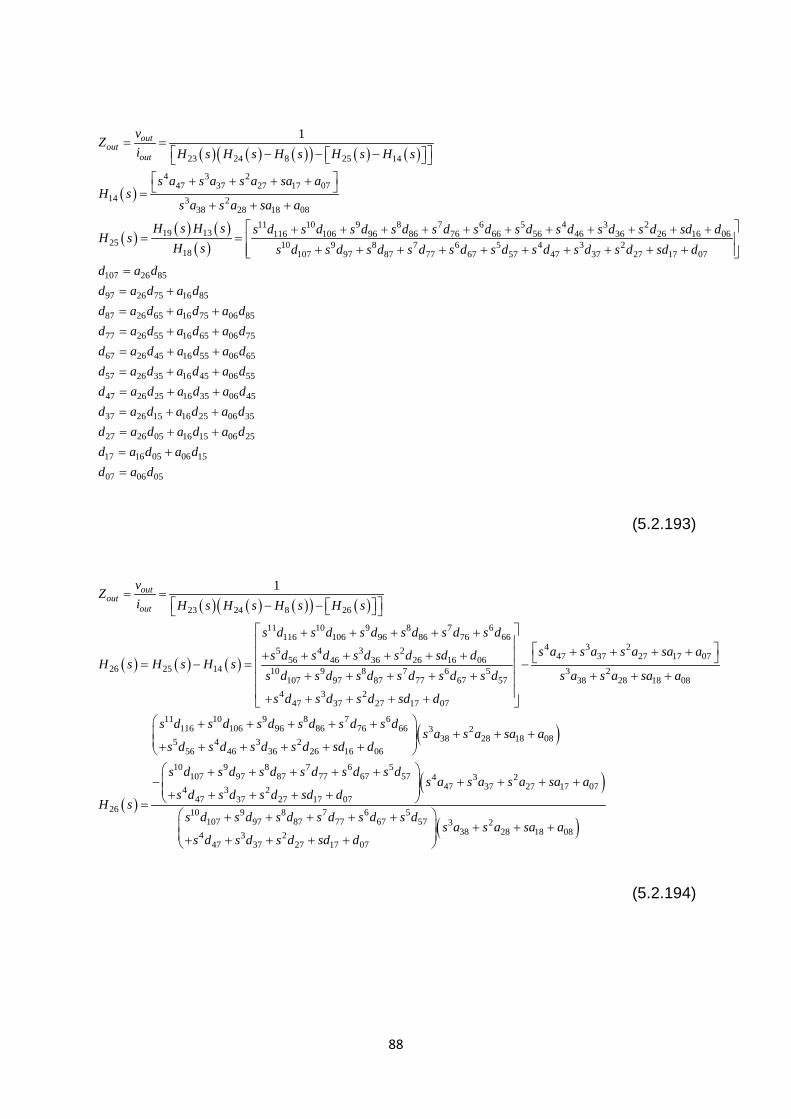
88
( ) ( ) ( )( ) ( ) ( )
( )
( ) ( ) ( )( )
23 24 8 25 14
4 3 247 37 27 17 07
14 3 238 28 18 08
11 10 9 8 7 6 5 4 3 219 13 116 106 96 86 76 66 56 46 36 26 16 06
25 10 918 107
1= =
− − − + + + + =
+ + +
+ + + + + + + + + + += =
+
outout
out
vZ
i H s H s H s H s H s
s a s a s a sa aH s
s a s a sa a
H s H s s d s d s d s d s d s d s d s d s d s d sd dH s
H s s d s 8 7 6 5 4 3 297 87 77 67 57 47 37 27 17 07
107 26 85
97 26 75 16 85
87 26 65 16 75 06 85
77 26 55 16 65 06 75
67 26 45 16 55 06 65
57 26 35 16 45 06 55
47 26 25 16
+ + + + + + + + + =
= +
= + +
= + +
= + +
= + +
= +
d s d s d s d s d s d s d s d sd dd a dd a d a dd a d a d a dd a d a d a dd a d a d a dd a d a d a dd a d a 35 06 45
37 26 15 16 25 06 35
27 26 05 16 15 06 25
17 16 05 06 15
07 06 05
+
= + +
= + +
= +
=
d a dd a d a d a dd a d a d a dd a d a dd a d
(5.2.193)
( ) ( ) ( )( ) ( )
( ) ( ) ( )
23 24 8 26
11 10 9 8 7 6116 106 96 86 76 66
5 4 3 256 46 36 26 16 06
26 25 14 10 9 8 7 6 5107 97 87 77 67 57
4 3 247 37 27 17 07
1= =
− − + + + + ++ + + + + +
= − = + + + + + + + + + +
outout
out
vZ
i H s H s H s H s
s d s d s d s d s d s d
s d s d s d s d sd dH s H s H s
s d s d s d s d s d s d
s d s d s d sd d
( )
( )
4 3 247 37 27 17 07
3 238 28 18 08
11 10 9 8 7 6116 106 96 86 76 66 3 2
38 28 18 085 4 3 256 46 36 26 16 06
10 9 8 7 6 5107 97 87 77 67 57
26
+ + + + − + + +
+ + + + + + + + + + + + + +
+ + + + +−
+=
s a s a s a sa a
s a s a sa a
s d s d s d s d s d s ds a s a sa a
s d s d s d s d sd d
s d s d s d s d s d s d
H s( )
( )
4 3 247 37 27 17 074 3 2
47 37 27 17 0710 9 8 7 6 5
107 97 87 77 67 57 3 238 28 18 084 3 2
47 37 27 17 07
+ + + + + + + +
+ + + + + + + + + + + + +
s a s a s a sa as d s d s d sd d
s d s d s d s d s d s ds a s a sa a
s d s d s d sd d
(5.2.194)
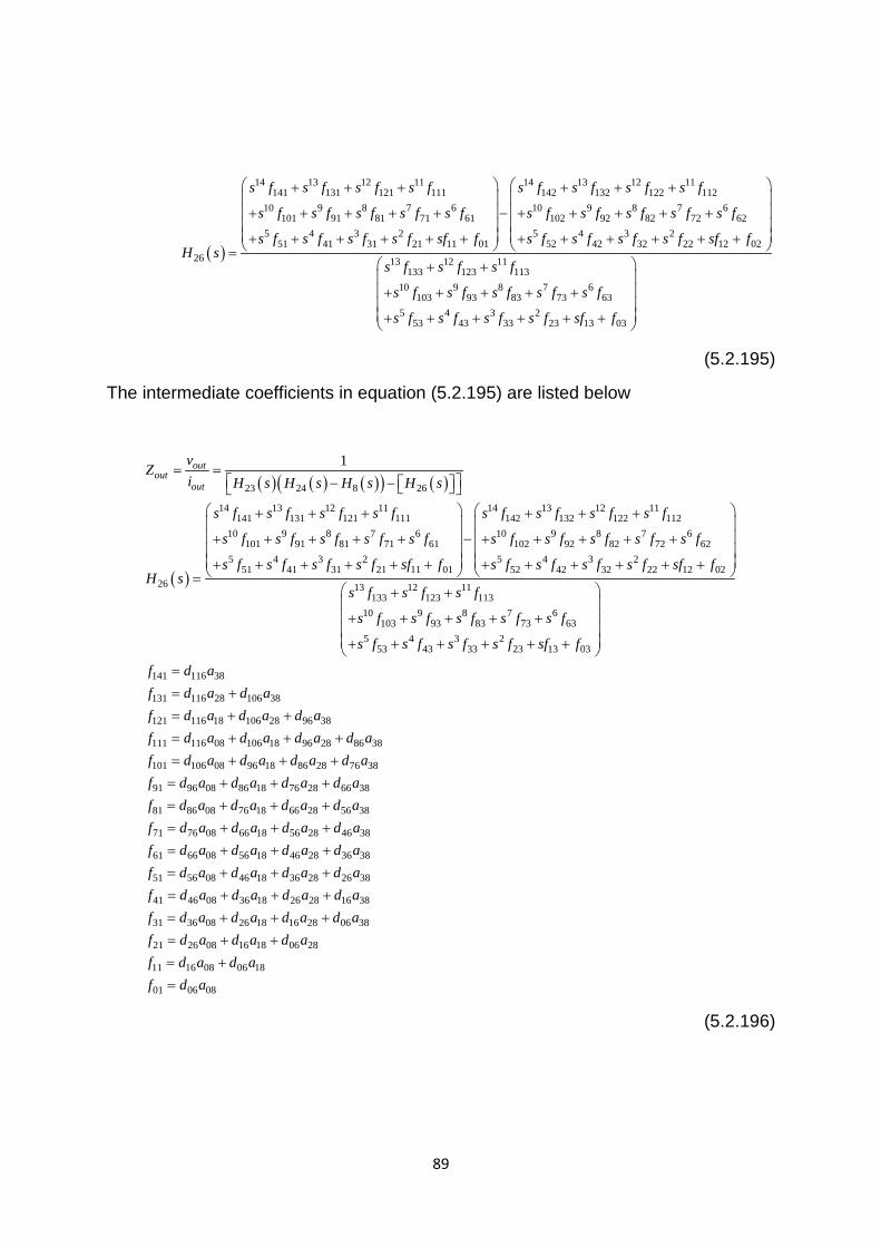
89
( )
14 13 12 11 14 13 12 11141 131 121 111 142 132 122 112
10 9 8 7 6 10 9 8 7 6101 91 81 71 61 102 92 82 72 62
5 4 3 2 5 4 3 251 41 31 21 11 01 52 42 32 2
26
+ + + + + + + + + + + − + + + + + + + + + + + + + + + =
s f s f s f s f s f s f s f s f
s f s f s f s f s f s f s f s f s f s f
s f s f s f s f sf f s f s f s f s fH s
2 12 02
13 12 11133 123 113
10 9 8 7 6103 93 83 73 63
5 4 3 253 43 33 23 13 03
+ +
+ + + + + + + + + + + + +
sf f
s f s f s f
s f s f s f s f s f
s f s f s f s f sf f
(5.2.195)
The intermediate coefficients in equation (5.2.195) are listed below
( ) ( ) ( )( ) ( )
( )
23 24 8 26
14 13 12 11 14 13 12 11141 131 121 111 142 132 122 112
10 9 8 7 6 10 9101 91 81 71 61 102 92
5 4 3 251 41 31 21 11 01
26
1= =
− − + + + + + + + + + + + − + + + + + + + + + =
outout
out
vZ
i H s H s H s H s
s f s f s f s f s f s f s f s f
s f s f s f s f s f s f s f
s f s f s f s f sf fH s
8 7 682 72 62
5 4 3 252 42 32 22 12 02
13 12 11133 123 113
10 9 8 7 6103 93 83 73 63
5 4 3 253 43 33 23 13 03
141 116 38
131 116 28 106 38
121
+ + + + + + + +
+ + + + + + + + + + + + +
=
= +
=
s f s f s f
s f s f s f s f sf f
s f s f s f
s f s f s f s f s f
s f s f s f s f sf f
f d af d a d af d116 18 106 28 96 38
111 116 08 106 18 96 28 86 38
101 106 08 96 18 86 28 76 38
91 96 08 86 18 76 28 66 38
81 86 08 76 18 66 28 56 38
71 76 08 66 18 56 28 46 38
61 66 08 56 18
+ +
= + + +
= + + +
= + + +
= + + +
= + + +
= + +
a d a d af d a d a d a d af d a d a d a d af d a d a d a d af d a d a d a d af d a d a d a d af d a d a d46 28 36 38
51 56 08 46 18 36 28 26 38
41 46 08 36 18 26 28 16 38
31 36 08 26 18 16 28 06 38
21 26 08 16 18 06 28
11 16 08 06 18
01 06 08
+
= + + +
= + + +
= + + +
= + +
= +
=
a d af d a d a d a d af d a d a d a d af d a d a d a d af d a d a d af d a d af d a
(5.2.196)
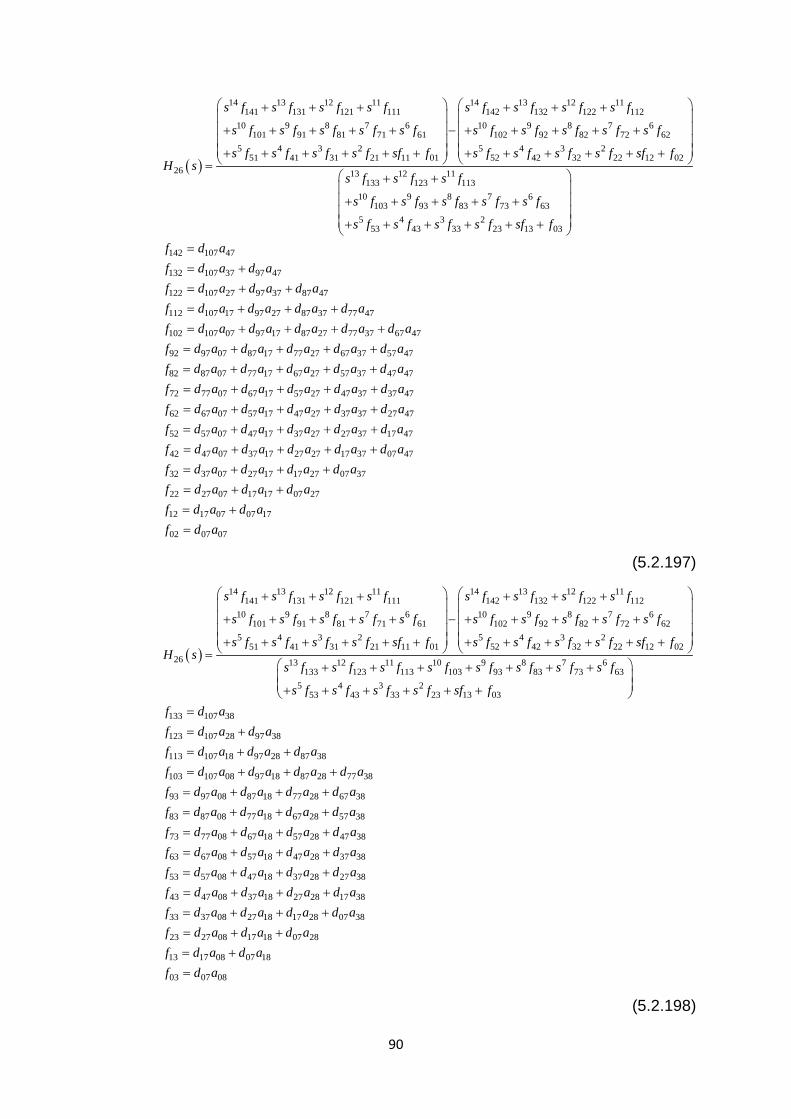
90
( )
14 13 12 11 14 13 12 11141 131 121 111 142 132 122 112
10 9 8 7 6 10 9 8 7 6101 91 81 71 61 102 92 82 72 62
5 4 3 2 5 4 3 251 41 31 21 11 01 52 42 32 2
26
+ + + + + + + + + + + − + + + + + + + + + + + + + + + =
s f s f s f s f s f s f s f s f
s f s f s f s f s f s f s f s f s f s f
s f s f s f s f sf f s f s f s f s fH s
2 12 02
13 12 11133 123 113
10 9 8 7 6103 93 83 73 63
5 4 3 253 43 33 23 13 03
142 107 47
132 107 37 97 47
122 107 27 97 37 87 47
112 107 17 97 27
+ +
+ + + + + + + + + + + + +
=
= +
= + +
= + +
sf f
s f s f s f
s f s f s f s f s f
s f s f s f s f sf f
f d af d a d af d a d a d af d a d a d87 37 77 47
102 107 07 97 17 87 27 77 37 67 47
92 97 07 87 17 77 27 67 37 57 47
82 87 07 77 17 67 27 57 37 47 47
72 77 07 67 17 57 27 47 37 37 47
62 67 07 57 17 47 27 37 37 2
+
= + + + +
= + + + +
= + + + +
= + + + +
= + + + +
a d af d a d a d a d a d af d a d a d a d a d af d a d a d a d a d af d a d a d a d a d af d a d a d a d a d 7 47
52 57 07 47 17 37 27 27 37 17 47
42 47 07 37 17 27 27 17 37 07 47
32 37 07 27 17 17 27 07 37
22 27 07 17 17 07 27
12 17 07 07 17
02 07 07
= + + + +
= + + + +
= + + +
= + +
= +
=
af d a d a d a d a d af d a d a d a d a d af d a d a d a d af d a d a d af d a d af d a
(5.2.197)
( )
14 13 12 11 14 13 12 11141 131 121 111 142 132 122 112
10 9 8 7 6 10 9 8 7 6101 91 81 71 61 102 92 82 72 62
5 4 3 2 5 4 3 251 41 31 21 11 01 52 42 32 2
26
+ + + + + + + + + + + − + + + + + + + + + + + + + + + =
s f s f s f s f s f s f s f s f
s f s f s f s f s f s f s f s f s f s f
s f s f s f s f sf f s f s f s f s fH s
2 12 02
13 12 11 10 9 8 7 6133 123 113 103 93 83 73 63
5 4 3 253 43 33 23 13 03
133 107 38
123 107 28 97 38
113 107 18 97 28 87 38
103 107 08 97 18 87 2
+ +
+ + + + + + + + + + + + +
=
= +
= + +
= + +
sf f
s f s f s f s f s f s f s f s f
s f s f s f s f sf ff d af d a d af d a d a d af d a d a d a 8 77 38
93 97 08 87 18 77 28 67 38
83 87 08 77 18 67 28 57 38
73 77 08 67 18 57 28 47 38
63 67 08 57 18 47 28 37 38
53 57 08 47 18 37 28 27 38
43 47 08 37 18 27 28 17 38
33 3
+
= + + +
= + + +
= + + +
= + + +
= + + +
= + + +
=
d af d a d a d a d af d a d a d a d af d a d a d a d af d a d a d a d af d a d a d a d af d a d a d a d af d 7 08 27 18 17 28 07 38
23 27 08 17 18 07 28
13 17 08 07 18
03 07 08
+ + +
= + +
= +
=
a d a d a d af d a d a d af d a d af d a
(5.2.198)
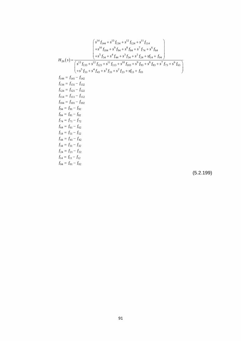
91
( )
14 13 12 11144 134 124 114
10 9 8 7 6104 94 84 74 64
5 4 3 254 44 34 24 14 04
26 13 12 11 10 9 8 7 6133 123 113 103 93 83 73 63
5 4 3 253 43 33 23 13 0
+ + + + + + + + + + + + + + =
+ + + + + + +
+ + + + + +
s f s f s f s f
s f s f s f s f s f
s f s f s f s f sf fH s
s f s f s f s f s f s f s f s f
s f s f s f s f sf f 3
144 141 142
134 131 132
124 121 122
114 111 112
104 101 102
94 91 92
84 81 82
74 71 72
64 61 62
54 51 52
44 41 42
34 31 32
24 21 22
14 11 12
04 01 02
= −= −
= −= −= −
= −
= −
= −
= −
= −
= −= −
= −= −= −
f f ff f ff f ff f ff f ff f ff f ff f ff f ff f ff f ff f ff f ff f ff f f
(5.2.199)
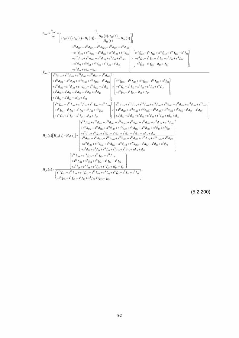
92
( ) ( ) ( )( ) ( ) ( )( ) ( )19 13
23 24 8 1418
22 21 20 19 18223 213 203 193 183
17 16 15 14 13173 163 153 143 133
12 11 10 9 8123 113 103 93 83
7 6 573 63 53
1= =
− − −
+ + + +
+ + + + +
+ + + + +
+ + + +
=
outout
out
out
vZi H s H s
H s H s H s H sH s
s d s d s d s d s d
s d s d s d s d s d
s d s d s d s d s d
s d s d s d
Z
13 12 11 10 9133 123 113 103 93
8 7 6 5 483 73 63 53 43
4 3 3 243 33 33 23 13 03
223 13 03
23 22 21 20 19232 222 212 202 192
18 17182 1
+ + + + × + + + + +
+ + + + + + + +
+ + + +
+ +
s f s f s f s f s f
s f s f s f s f s f
s d s d s f s f sf f
s d sd d
s d s d s d s d s d
s d s d 16 15 14 13 12 11 10 972 162 152 142 133 123 113 103 93
13 12 11 10 9 8 7 6 5 4132 122 112 102 92 83 73 63 53
8 7 6 5 482 72 62 52 42
3 232 22 12 02
+ + + + + + + + + + + + × + + + + + + + + + + + + + +
s d s d s d s f s f s f s f s f
s d s d s d s d s d s f s f s f s f s
s d s d s d s d s d
s d s d sd d
433 2
33 23 13 03
14 13 12 11 10 22 21 20 19 18 17 16144 134 124 114 104 223 213 203 193 183 173 16
9 8 7 6 594 84 74 64 54
4 3 244 34 24 14 04
+ + + +
+ + + + + + + + + + − + + + + + × + + + + +
f
s f s f sf f
s f s f s f s f s f s d s d s d s d s d s d s d
s f s f s f s f s f
s f s f s f sf f
( ) ( ) ( )
153 153
14 13 12 11 10 9 8 7143 133 123 113 103 93 83 73
6 5 4 3 263 53 43 33 23 13 03
23 22 21 20 19 18 17 16232 222 212 202 192 182 172 162
23 24 8
+ + + + + + + + + + + + + + + +
+ + + + + + +
+
− =
s d
s d s d s d s d s d s d s d s d
s d s d s d s d s d sd d
s d s d s d s d s d s d s d s d
s
H s H s H s
15 14 13 12 11 10 9 8152 142 132 122 112 102 92 82
7 6 5 4 3 272 62 52 42 32 22 12 02
22 21 20 19 18 17 16 15223 213 203 193 183 173 163 153
14 13 12 11143 133 123 113
+ + + + + + +
+ + + + + + + ++ + + + + + +
+ + + + +
d s d s d s d s d s d s d s d
s d s d s d s d s d s d sd ds d s d s d s d s d s d s d s d
s d s d s d s d s
( )
10 9 8 7103 93 83 73
6 5 4 3 263 53 43 33 23 13 03
14 13 12 11144 134 124 114
10 9 8 7 6104 94 84 74 64
5 4 3 254 44 34 24 14 04
26 1
+ + + + + + + + + +
+ + + + + + + + + + + + + + =
d s d s d s d
s d s d s d s d s d sd d
s f s f s f s f
s f s f s f s f s f
s f s f s f s f sf fH s
s 3 12 11 10 9 8 7 6133 123 113 103 93 83 73 63
5 4 3 253 43 33 23 13 03
+ + + + + + + + + + + + +
f s f s f s f s f s f s f s f
s f s f s f s f sf f
(5.2.200)
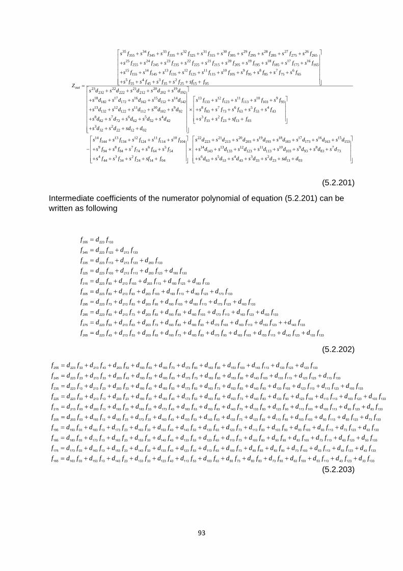
93
35 34 33 32 31 30 29 28 27 26355 345 335 325 315 305 295 285 275 265
25 24 23 22 21 20 19 18 17 16255 245 235 225 215 205 195 185 175 165
15 14 13 12 11155 145 135 125
+ + + + + + + + +
+ + + + + + + + + +
+ + + + +
=out
s f s f s f s f s f s f s f s f s f s f
s f s f s f s f s f s f s f s f s f s f
s f s f s f s f s
Z
10 9 8 7 6115 105 95 85 75 65
5 4 3 255 45 35 25 15 05
23 22 21 20 19232 222 212 202 192
18 17 16 15 14182 172 162 152 142
13 12 11 10 9132 122 112 102
+ + + + + + + + + + +
+ + + +
+ + + + +
+ + + + +
f s f s f s f s f s f
s f s f s f s f sf fs d s d s d s d s d
s d s d s d s d s d
s d s d s d s d s d
13 12 11 10 9133 123 113 103 93
8 7 6 5 492 83 73 63 53 43
8 7 6 5 4 3 282 72 62 52 42 33 23 13 03
3 232 22 12 02
14 13 12144 134 124
+ + + + × + + + + +
+ + + + + + + + + + + + +
+ + +
−
s f s f s f s f s f
s f s f s f s f s f
s d s d s d s d s d s f s f sf f
s d s d sd d
s f s f s f s11 10 22 21 20 19 18 17 16 15114 104 223 213 203 193 183 173 163 153
9 8 7 6 5 14 13 12 11 10 9 894 84 74 64 54 143 133 123 113 103 93 83
4 3 244 34 24 14 04
+ + + + + + + + + + + + + × + + + + + + + + + + + + +
f s f s d s d s d s d s d s d s d s d
s f s f s f s f s f s d s d s d s d s d s d s d
s f s f s f sf f
773
6 5 4 3 263 53 43 33 23 13 03
+ + + + + + +
s d
s d s d s d s d s d sd d
(5.2.201)
Intermediate coefficients of the numerator polynomial of equation (5.2.201) can be written as following
== += + += + + += + + + += + + + +
355 223 133
345 223 123 213 133
335 223 113 213 123 203 133
325 223 103 213 113 203 123 193 133
315 223 93 213 103 203 113 193 123 183 133
305 223 83 213 93 203 103 193 113 183 12
f d ff d f d ff d f d f d ff d f d f d f d ff d f d f d f d f d ff d f d f d f d f d f +
= + + + + + += + + + + + + += + + + + + +
3 173 133
295 223 73 213 83 203 93 193 103 183 113 173 123 163 133
285 223 63 213 73 203 83 193 93 183 103 173 113 163 123 153 133
275 223 53 213 63 203 73 193 83 183 93 173 103
d ff d f d f d f d f d f d f d ff d f d f d f d f d f d f d f d ff d f d f d f d f d f d f + + +
= + + + + + + + + +163 113 153 123 143 133
265 223 43 213 53 203 63 193 73 183 83 173 93 163 103 153 113 143 123 133 133
d f d f d ff d f d f d f d f d f d f d f d f d f d f
(5.2.202)
= + + + + + + + + + += + + + + + + + + + + +
255 223 33 213 43 203 53 193 63 183 73 173 83 163 93 153 103 143 113 133 123 123 133
245 223 23 213 33 203 43 193 53 183 63 173 73 163 83 153 93 143 103 133 113 123 123 113 133
f d f d f d f d f d f d f d f d f d f d f d ff d f d f d f d f d f d f d f d f d f d f d f d f
= + + + + + + + + + + + += + + + + + + + + + +
235 223 13 213 23 203 33 193 43 183 53 173 63 163 73 153 83 143 93 133 103 123 113 113 123 103 133
225 223 03 213 13 203 23 193 33 183 43 173 53 163 63 153 73 143 83 133 93 12
f d f d f d f d f d f d f d f d f d f d f d f d f d ff d f d f d f d f d f d f d f d f d f d f d + + +
= + + + + + + + + + + + + += + + + + +
3 103 113 113 103 123 103 133
215 213 03 203 13 193 23 183 33 173 43 163 53 153 63 143 73 133 83 123 93 113 103 103 113 93 123 83 133
205 203 03 193 13 183 23 173 33 163 43 153
f d f d f d ff d f d f d f d f d f d f d f d f d f d f d f d f d f d ff d f d f d f d f d f d f + + + + + + + +
= + + + + + + + + + + + + += +
53 143 63 133 73 123 83 113 93 103 103 93 113 83 123 73 133
195 193 03 183 13 173 23 163 33 153 43 143 53 133 63 123 73 113 83 103 93 93 103 83 113 73 123 63 133
185 183 03 173
d f d f d f d f d f d f d f d ff d f d f d f d f d f d f d f d f d f d f d f d f d f d ff d f d + + + + + + + + + + + +
= + + + + + + + + + + + +13 163 23 153 33 143 43 133 53 123 63 113 73 103 83 93 93 83 103 73 113 63 123 53 133
175 173 03 163 13 153 23 143 33 133 43 123 53 113 63 103 73 93 83 83 93 73 103 63 113 53
f d f d f d f d f d f d f d f d f d f d f d f d ff d f d f d f d f d f d f d f d f d f d f d f d f d +
= + + + + + + + + + + + + +123 43 133
165 163 03 153 13 143 23 133 33 123 43 113 53 103 63 93 73 83 83 73 93 63 103 53 113 43 123 33 133
f d ff d f d f d f d f d f d f d f d f d f d f d f d f d f d f
(5.2.203)
94
f d f d f d f d f d f d f d f d f d f d f d f d f d f d ff d f d f d f d f d f d f d f d f d f d f d f
= + + + + + + + + + + + + += + + + + + + + + + + +
155 153 03 143 13 133 23 123 33 113 43 103 53 93 63 83 73 73 83 63 93 53 103 43 113 33 123 23 133
145 143 03 133 13 123 23 113 33 103 43 93 53 83 63 73 73 63 83 53 93 43 103 d f d f d ff d f d f d f d f d f d f d f d f d f d f d f d f d f d ff d f d f d f d f d f d f d f d f d
+ += + + + + + + + + + + + + += + + + + + + + +
33 113 23 123 13 133
135 133 03 123 13 113 23 103 33 93 43 83 53 73 63 63 73 53 83 43 93 33 103 23 113 13 123 03 133
125 123 03 113 13 103 23 93 33 83 43 73 53 63 63 53 73 43 f d f d f d f d ff d f d f d f d f d f d f d f d f d f d f d f d ff d f d f d f d f d f d f d f d f d f d f
+ + + += + + + + + + + + + + += + + + + + + + + +
83 33 93 23 103 13 113 03 123
115 113 03 103 13 93 23 83 33 73 43 63 53 53 63 43 73 33 83 23 93 13 103 03 113
105 103 03 93 13 83 23 73 33 63 43 53 53 43 63 33 73 23 83 13 9 d ff d f d f d f d f d f d f d f d f d f d ff d f d f d f d f d f d f d f d f d ff d f d f d f d f d f d f d f
+= + + + + + + + + += + + + + + + + += + + + + + +
3 03 103
95 93 03 83 13 73 23 63 33 53 43 43 53 33 63 23 73 13 83 03 93
85 83 03 73 13 63 23 53 33 43 43 33 53 23 63 13 73 03 83
75 73 03 63 13 53 23 43 33 33 43 23 53 13 63 d ff d f d f d f d f d f d f d f
+= + + + + + +
03 73
65 63 03 53 13 43 23 33 33 23 43 13 53 03 63
(5.2.204)
f d f d f d f d f d f d ff d f d f d f d f d ff d f d f d f d ff d f d f d ff d f d ff d f
= + + + + += + + + += + + += + += +=
55 53 03 43 13 33 23 23 33 13 43 03 53
45 43 03 33 13 23 23 13 33 03 43
35 33 03 23 13 13 23 03 33
25 23 03 13 13 03 23
15 13 03 03 13
05 03 03
(5.2.205)
Intermediate coefficients of the denominator polynomial of equation (5.2.201) can be written as following
f d ff d f d ff d f d f d ff d f d f d f d ff d f d f d f d f d ff d f d f d f d f d f
== += + += + + += + + + += + + + +
366 232 133
356 232 123 222 133
346 232 113 222 123 212 133
336 232 103 222 113 212 123 202 133
326 232 93 222 103 212 113 202 123 192 133
316 232 83 222 93 212 103 202 113 192 12 d ff d f d f d f d f d f d f d ff d f d f d f d f d f d f d f d ff d f d f d f d f d f d f
+= + + + + + += + + + + + + += + + + + + +
3 182 133
306 232 73 222 83 212 93 202 103 192 113 182 123 172 133
296 232 63 222 73 212 83 202 93 192 103 182 113 172 123 162 133
286 232 53 222 63 212 73 202 83 192 93 182 103 d f d f d ff d f d f d f d f d f d f d f d f d f d f
+ += + + + + + + + + +
172 113 162 123 152 133
276 232 43 222 53 212 63 202 73 192 83 182 93 172 103 162 113 152 123 142 133
(5.2.206)
95
f d f d f d f d f d f d f d f d f d f d f d ff d f d f d f d f d f d f d f d f d f d f d f d f
= + + + + + + + + + += + + + + + + + + + + +
266 232 33 222 43 212 53 202 63 192 73 182 83 172 93 162 103 152 113 142 123 132 133
256 232 23 222 33 212 43 202 53 192 63 182 73 172 83 162 93 152 103 142 113 132 123 122 133
f d f d f d f d f d f d f d f d f d f d f d f d f d ff d f d f d f d f d f d f d f d f d f d f d
= + + + + + + + + + + + += + + + + + + + + + +
246 232 13 222 23 212 33 202 43 192 53 182 63 172 73 162 83 152 93 142 103 132 113 122 123 112 133
236 232 03 222 13 212 23 202 33 192 43 182 53 172 63 162 73 152 83 142 93 13 f d f d f d ff d f d f d f d f d f d f d f d f d f d f d f d f d f d ff d f d f d f d f d f d
+ + += + + + + + + + + + + + + += + + + + +
2 103 122 113 112 123 102 133
226 222 03 212 13 202 23 192 33 182 43 172 53 162 63 152 73 142 83 132 93 122 103 112 113 102 123 92 133
216 212 03 202 13 192 23 182 33 172 43 162 f d f d f d f d f d f d f d f d ff d f d f d f d f d f d f d f d f d f d f d f d f d f d ff d f d
+ + + + + + + += + + + + + + + + + + + + += +
53 152 63 142 73 132 83 122 93 112 103 102 113 92 123 82 133
206 202 03 192 13 182 23 172 33 162 43 152 53 142 63 132 73 122 83 112 93 102 103 92 113 82 123 72 133
196 192 03 f d f d f d f d f d f d f d f d f d f d f d f d ff d f d f d f d f d f d f d f d f d f d f d f d f
+ + + + + + + + + + + += + + + + + + + + + + +
182 13 172 23 162 33 152 43 142 53 132 63 122 73 112 83 102 93 92 103 82 113 72 123 62 133
186 182 03 172 13 162 23 152 33 142 43 132 53 122 63 112 73 102 83 92 93 82 103 72 11 d f d ff d f d f d f d f d f d f d f d f d f d f d f d f d f d f
+ += + + + + + + + + + + + + +
3 62 123 52 133
176 172 03 162 13 152 23 142 33 132 43 122 53 112 63 102 73 92 83 82 93 72 103 62 113 52 123 42 133
(5.2.207)
f d f d f d f d f d f d f d f d f d f d f d f d f d f d ff d f d f d f d f d f d f d f d f d f d f d f
= + + + + + + + + + + + + += + + + + + + + + + +
166 162 03 152 13 142 23 132 33 122 43 112 53 102 63 92 73 82 83 72 93 62 103 52 113 42 123 32 133
156 152 03 142 13 132 23 122 33 112 43 102 53 92 63 82 73 72 83 62 93 52 10 d f d f d ff d f d f d f d f d f d f d f d f d f d f d f d f d f d ff d f d f d f d f d f d f d f d f
+ + += + + + + + + + + + + + + += + + + + + + +
3 42 113 32 123 22 133
146 142 03 132 13 122 23 112 33 102 43 92 53 82 63 72 73 62 83 52 93 42 103 32 113 22 123 12 133
136 132 03 122 13 112 23 102 33 92 43 82 53 72 63 62 73 d f d f d f d f d f d ff d f d f d f d f d f d f d f d f d f d f d f d f d ff d f d f d f d f d f d f d f
+ + + + + += + + + + + + + + + + + += + + + + + +
52 83 42 93 32 103 22 113 12 123 02 133
126 122 03 112 13 102 23 92 33 82 43 72 53 62 63 52 73 42 83 32 93 22 103 12 113 02 123
116 112 03 102 13 92 23 82 33 72 43 62 53 52 d f d f d f d f d ff d f d f d f d f d f d f d f d f d f d f d ff d f d f d f d f d f d f d f d f d f d ff d
+ + + + += + + + + + + + + + += + + + + + + + + +=
63 42 73 32 83 22 93 12 103 02 113
106 102 03 92 13 82 23 72 33 62 43 52 53 42 63 32 73 22 83 12 93 02 103
96 92 03 82 13 72 23 62 33 52 43 42 53 32 63 22 73 12 83 02 93
86 f d f d f d f d f d f d f d f d ff d f d f d f d f d f d f d f d f
+ + + + + + + += + + + + + + +
82 03 72 13 62 23 52 33 42 43 32 53 22 63 12 73 02 83
76 72 03 62 13 52 23 42 33 32 43 22 53 12 63 02 73
(5.2.208)
f d f d f d f d f d f d f d ff d f d f d f d f d f d ff d f d f d f d f d ff d f d f d f d ff d f d f d ff d f
= + + + + + += + + + + += + + + += + + += + +=
66 62 03 52 13 42 23 32 33 22 43 12 53 02 63
56 52 03 42 13 32 23 22 33 12 43 02 53
46 42 03 32 13 22 23 12 33 02 43
36 32 03 22 13 12 23 02 33
26 22 03 12 13 02 23
16 12 03 d ff d f
+=
02 13
06 02 03
(5.2.209)
96
35 34 33 32 31 30 29 28 27 26355 345 335 325 315 305 295 285 275 265
25 24 23 22 21 20 19 18 17 16255 245 235 225 215 205 195 185 175 165
15 14 13 12 11155 145 135 125
out
s f s f s f s f s f s f s f s f s f s f
s f s f s f s f s f s f s f s f s f s f
s f s f s f s f s
Z
+ + + + + + + + +
+ + + + + + + + + +
+ + + + +
=
10 9 8 7 6115 105 95 85 75 65
5 4 3 255 45 35 25 15 05
36 35 34 33 32 31 30 29 28 27366 356 346 336 326 316 306 296 286 276
26 25 24 23 22266 256 246 236
f s f s f s f s f s f
s f s f s f s f sf fs f s f s f s f s f s f s f s f s f s f
s f s f s f s f s
+ + + + + + + + + + +
+ + + + + + + + +
+ + + + + 21 20 19 18 17226 216 206 196 186 176
16 15 14 13 12 11 10 9 8 7166 156 146 136 126 116 106 96 86 76
6 5 4 3 266 56 46 36 26 16 06
36 35 34 3367 357 347
f s f s f s f s f s f
s f s f s f s f s f s f s f s f s f s f
s f s f s f s f s f sf f
s f s f s f s
+ + + + + + + + + + + + + + + + + + + + + +
+ + +
−
3 32 31 30 29 28 27337 327 317 307 297 287 277
26 25 24 23 22 21 20 19 18 17267 257 247 237 227 217 207 197 187 177
16 15 14 13 12 11 10 9 8167 157 147 137 127 117 107 97 8
f s f s f s f s f s f s f
s f s f s f s f s f s f s f s f s d s f
s f s f s f s f s f s f s f s f s f
+ + + + + +
+ + + + + + + + + +
+ + + + + + + + + 77 77
6 5 4 3 267 57 47 37 27 17 07
s f
s f s f s f s f s f sf f
+ + + + + + + +
(5.2.210)
f f df f d f df f d f d f df f d f d f d f df f d f d f d f d f df f d f d f d f d f
== += + += + + += + + + += + + + +
367 144 223
357 144 213 134 223
347 144 203 134 213 124 223
337 144 193 134 203 124 213 114 223
327 144 183 134 193 124 203 114 213 104 223
317 144 173 134 183 124 193 114 203 104d f df f d f d f d f d f d f d f df f d f d f d f d f d f d f d f df f d f d f d f d f d
+= + + + + + += + + + + + + += + + + + +
213 94 223
307 144 163 134 173 124 183 114 193 104 203 94 213 84 223
297 144 153 134 163 124 173 114 183 104 193 94 203 84 213 74 223
287 144 143 134 153 124 163 114 173 104 183 f d f d f d f df f d f d f d f d f d f d f d f d f d f d
+ + += + + + + + + + + +
94 193 84 203 74 213 64 223
277 144 133 134 143 124 153 114 163 104 173 94 183 84 193 74 203 64 213 54 223
(5.2.211)
f f d f d f d f d f d f d f d f d f d f d f df f d f d f d f d f d f d f d f d f d f d f d f d
= + + + + + + + + + += + + + + + + + + + + +
267 144 123 134 133 124 143 114 153 104 163 94 173 84 183 74 193 64 203 54 213 44 223
257 144 113 134 123 124 133 114 143 104 153 94 163 84 173 74 183 64 193 54 203 44 213 34 2
f f d f d f d f d f d f d f d f d f d f d f d f d f df f d f d f d f d f d f d f d f d f d f d
= + + + + + + + + + + + += + + + + + + + + +
23
247 144 103 134 113 124 123 114 133 104 143 94 153 84 163 74 173 64 183 54 193 44 203 34 213 24 223
237 144 93 134 103 124 113 114 123 104 133 94 143 84 153 74 163 64 173 54 f d f d f d f df f d f d f d f d f d f d f d f d f d f d f d f d f d f d
f df f d f d f d f d
+ + + += + + + + + + + + + + + + +
+= + + + +
183 44 193 34 203 24 213 14 223
227 144 83 134 93 124 103 114 113 104 123 94 133 84 143 74 153 64 163 54 173 44 183 34 193 24 203 14 213
04 223
217 144 73 134 83 124 93 114 103 f d f d f d f d f d f d f d f d f d f df d
f f d f d f d f d f d f d f d f d f d f d f d f d f d f
+ + + + + + + + ++
= + + + + + + + + + + + + +
104 113 94 123 84 133 74 143 64 153 54 163 44 173 34 183 24 193 14 203
04 213
207 144 63 134 73 124 83 114 93 104 103 94 113 84 123 74 133 64 143 54 153 44 163 34 173 24 183 1 df d
f f d f d f d f d f d f d f d f d f d f d f d f d f d f df d
f f d f d f d f d f d f d f d f
+= + + + + + + + + + + + + +
+= + + + + + + +
4 193
04 203
197 144 53 134 63 124 73 114 83 104 93 94 103 84 113 74 123 64 133 54 143 44 153 34 163 24 173 14 183
04 193
187 144 43 134 53 124 63 114 73 104 83 94 93 84 103 74d f d f d f d f d f d f df d
f f d f d f d f d f d f d f d f d f d f d f d f d f d f df d
+ + + + + ++
= + + + + + + + + + + + + ++
113 64 123 54 133 44 143 34 153 24 163 14 173
04 183
177 144 33 134 43 124 53 114 63 104 73 94 83 84 93 74 103 64 113 54 123 44 133 34 143 24 153 14 163
04 173
(5.2.212)
97
f f d f d f d f d f d f d f d f d f d f d f d f d f d f df d
f f d f d f d f d f d f d f d f d f d f d
= + + + + + + + + + + + + ++
= + + + + + + + + +
167 144 23 134 33 124 43 114 53 104 63 94 73 84 83 74 93 64 103 54 113 44 123 34 133 24 143 14 153
04 163
157 144 13 134 23 124 33 114 43 104 53 94 63 84 73 74 83 64 93 54 10 f d f d f d f df d
f f d f d f d f d f d f d f d f d f d f d f d f d f d f df d
f f d f d f d f d f
+ + + ++
= + + + + + + + + + + + + ++
= + + + +
3 44 113 34 123 24 133 14 143
04 153
147 144 03 134 13 124 23 114 33 104 43 94 53 84 63 74 73 64 83 54 93 44 103 34 113 24 123 14 133
04 143
137 134 03 124 13 114 23 104 33 94d f d f d f d f d f d f d f d f d f df f d f d f d f d f d f d f d f d f d f d f d f d f df f d f d f d f
+ + + + + + + + += + + + + + + + + + + + += + + +
43 84 53 74 63 64 73 54 83 44 93 34 103 24 113 14 123 04 133
127 124 03 114 13 104 23 94 33 84 43 74 53 64 63 54 73 44 83 34 93 24 103 14 113 04 123
117 114 03 104 13 94 23 d f d f d f d f d f d f d f d f df f d f d f d f d f d f d f d f d f d f d f df f d f d f d f d f d f d f d f
+ + + + + + + += + + + + + + + + + += + + + + + + +
84 33 74 43 64 53 54 63 44 73 34 83 24 93 14 103 04 113
107 104 03 94 13 84 23 74 33 64 43 54 53 44 63 34 73 24 83 14 93 04 103
97 94 03 84 13 74 23 64 33 54 43 44 53 34 63 d f d f df f d f d f d f d f d f d f d f d f df f d f d f d f d f d f d f d f df f d f d f d f d f d f d f d
+ += + + + + + + + += + + + + + + += + + + + + +
24 73 14 83 04 93
87 84 03 74 13 64 23 54 33 44 43 34 53 24 63 14 73 04 83
77 74 03 64 13 54 23 44 33 34 43 24 53 14 63 04 73
67 64 03 54 13 44 23 34 33 24 43 14 53 04 63
(5.2.213)
f f d f d f d f d f d f df f d f d f d f d f df f d f d f d f df f d f d f df f d f df f d
= + + + + += + + + += + + += + += +=
57 54 03 44 13 34 23 24 33 14 43 04 53
47 44 03 34 13 24 23 14 33 04 43
37 34 03 24 13 14 23 04 33
27 24 03 14 13 04 23
17 14 03 04 13
07 04 03
(5.2.214)
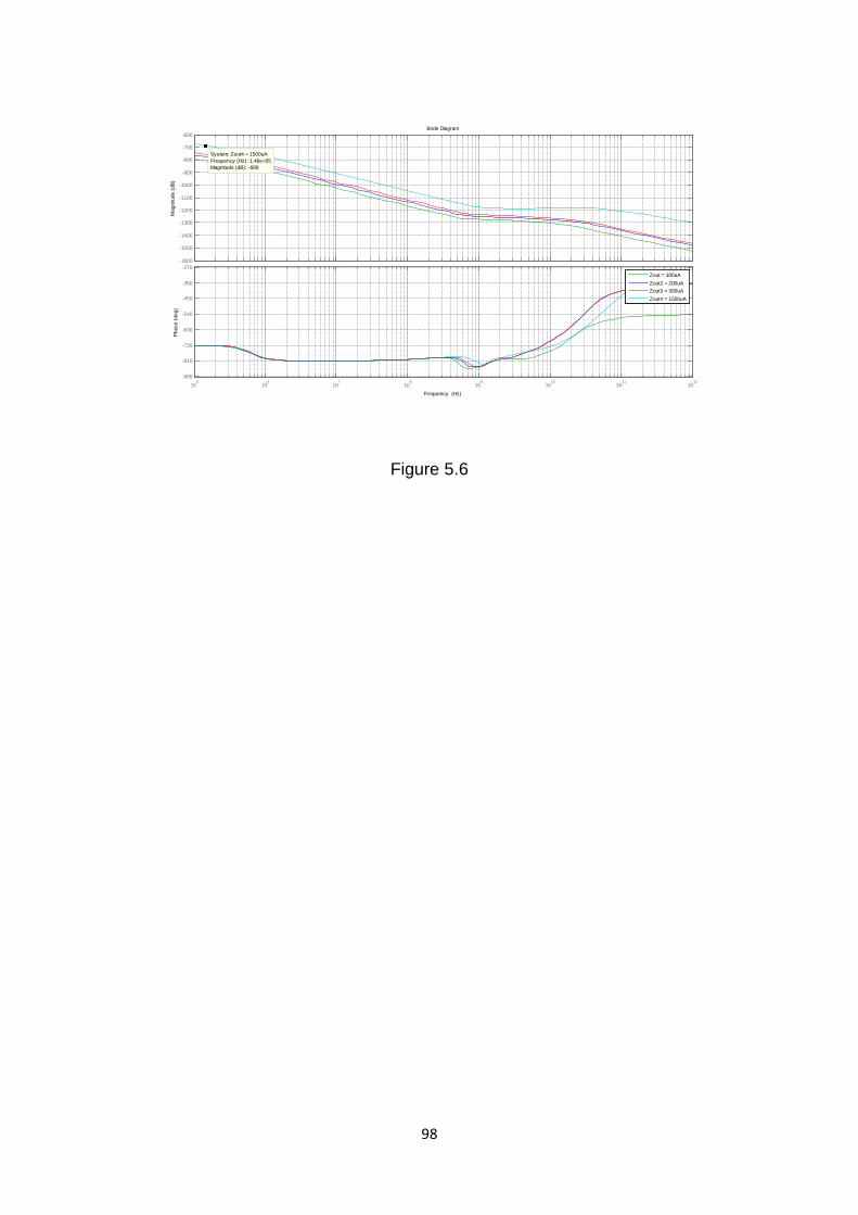
98
Figure 5.6
-1600
-1500
-1400
-1300
-1200
-1100
-1000
-900
-800
-700
-600
System: Zout4 = 1500uAFrequency (Hz): 1.46e+05Magnitude (dB): -689
Mag
nitu
de (d
B)
105
106
107
108
109
1010
1011
1012
-900
-810
-720
-630
-540
-450
-360
-270
Phas
e (d
eg)
Bode Diagram
Frequency (Hz)
Zout = 100uAZout2 = 200uAZout3 = 300uAZout4 = 1500uA
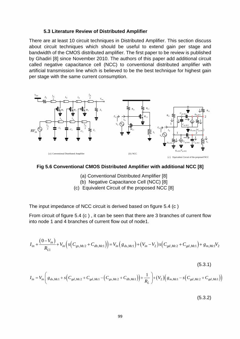
99
5.3 Literature Review of Distributed Amplifier
There are at least 10 circuit techniques in Distributed Amplifier. This section discuss about circuit techniques which should be useful to extend gain per stage and bandwidth of the CMOS distributed amplifier. The first paper to be review is published by Ghadiri [8] since November 2010. The authors of this paper add additional circuit called negative capacitance cell (NCC) to conventional distributed amplifier with artificial transmission line which is believed to be the best technique for highest gain per stage with the same current consumption.
inRF 2gL
0Z2dL
2dL
dL dL
gL gL
2gL
oZ1M 2M 3M
1C−2C−
3C− oZ
DDV
outV
1LR 2LR
inV
inIinZ
1L1CM
2CM
1L
1LR
2LR
inV
inIinZ
, 1gs McC
( ), 1 , 1m Mc gs Mcg V
1
2
2
, 2gd McC, 2ds Mcg
, 1 , 1m Mc gs Mcg V
1
, 1ds Mcg
, 2gs McC
, 1gd McC
( ) Conventional Distributed Amplifiera ( ) NCCb( ) Equivalent Circuit of the proposed NCCc
Fig 5.6 Conventional CMOS Distributed Amplifier with additional NCC [8]
(a) Conventional Distributed Amplifier [8] (b) Negative Capacitance Cell (NCC) [8]
(c) Equivalent Circuit of the proposed NCC [8]
The input impedance of NCC circuit is derived based on figure 5.4 (c )
From circuit of figure 5.4 (c ) , it can be seen that there are 3 branches of current flow into node 1 and 4 branches of current flow out of node1.
( ) ( )( ) ( ) ( ) ( ), 2 , 1 , 1 2 , 2 , 1 , 1 21
0 inin in gs Mc db Mc in ds Mc in gd Mc gd Mc m Mc
L
VI V s C C V g V V s C C g V
R−
+ + + = + − + +
(5.3.1)
( )( ) ( ) ( )( ), 1 , 2 , 1 , 2 , 1 2 , 1 , 2 , 11
in in ds Mc gd Mc gd Mc gs Mc db Mc m Mc gd Mc gd McL
I V g s C C C C V g s C CR
= + + − + + + − +
(5.3.2)
100
It can also be seen from figure 5.4 (c ) that there are 3 branches of current flow into node 2 and 4 branches of current flow out of node2
( ) ( ) ( ) ( )22 , 1 , 2 , 1 2 , 2 , 1 , 2
2 1
0 1in gd Mc gd Mc m Mc in db Mc gs Mc ds Mc
L
VV V s C C g V V s C C g
R sL−
− + + = + + + +
(5.3.3)
( ) ( )( )( ), 2 , 1 , 1 , 2
, 1 , 2 , 1 2, 2
1 2
1 1db Mc gs Mc gd Mc gd Mc
in gd Mc gd Mc m Mcds Mc
L
s C C C CV s C C g V
gsL R
+ + +
+ − = + + +
(5.3.4)
Multiply both sides of equation (5.3.4) with 1sL
( ) ( )( )( )
( )
21 , 2 , 1 , 1 , 2
21 , 1 , 2 1 , 1 2 1
1 , 22
1
db Mc gs Mc gd Mc gd Mc
in gd Mc gd Mc m Mcds Mc
L
s L C C C CV s L C C sL g V sLs L g
R
+ + +
+ − = + + +
(5.3.5)
To eliminate 2V , one can write ( )2 inV f V=
( )( )( )
( )
21 , 1 , 2 1 , 1
22 1
1 1 1 , 22
1 , 2 , 1 , 1 , 2
1
gd Mc gd Mc m Mcin
ds McL
db Mc gs Mc gd Mc gd Mc
s L C C sL gV V
sLs L C s L gR
C C C C C
+ −=
+ + +
= + + +
(5.3.6)
Substitute (5.3.6) into (5.3.2)
( ) ( )( )( )
( )( )( )
( )
21 , 1 , 2 1 , 1
, 1 2 , 1 , 2 , 12 1
1 1 1 , 22
2 , 2 , 1 , 2 , 1
1
1
gd Mc gd Mc m Mcin in ds Mc in m Mc gd Mc gd Mc
Lds Mc
L
gd Mc gd Mc gs Mc db Mc
s L C C sL gI V g s C V g s C C
R sLs L C s L gR
C C C C C
+ − = + + + − + + + +
= + − +
(5.3.7)
Multiply group of polynomial so that one can manipulate input impedance of this circuit as a general polynomial
101
( ) ( )
( )( ) ( )( )( )
2 1, 1 2 1 1 1 , 2
2
21 , 1 , 2 1 , 1 , 1 , 2 , 1
2 11 1 1 , 2
2
1 1
1
ds Mc ds McL L
gd Mc gd Mc m Mc m Mc gd Mc gd Mcin in
ds McL
sLg s C s L C s L gR R
s L C C sL g g s C CI V
sLs L C s L gR
+ + + + +
+ + − − + =
+ + +
(5.3.8)
( )
( )( )( ) ( )
3 2 12 1 1 1 1 , 1 2 1 , 2
2
12 1 , 2 , 1 , 1
2
3 21 , 1 , 2 , 2 , 1 1 , 1 , 2 , 1 1 , 1
1
1
ds Mc ds McL L
ds Mc ds Mc ds McL L
gd Mc gd Mc gd Mc gd Mc gd Mc gd Mc m Mc m Mc
in in
Ls C L C s L C g C L gR R
Ls C L g g gR R
s L C C C C s L C C g L g
I V
+ + + +
+ + + + +
− + + + + +
=
( )( ) ( )
( )
2, 2 , 1 1 , 1
2 11 1 1 , 2
21
gd Mc gd Mc m Mc
ds McL
C C s L g
sLs L C s L gR
+ −
+ + +
(5.3.9)
It can be seen that one have polynomial which can be grouped with the same order of polynomial.
( )( )( )( ) ( )
32 1 1 1 , 1 , 2 , 2 , 1
2 11 1 , 1 2 1 , 2 1 , 1 , 2 , 1 1 , 1 , 2 , 1
2
12 1 , 2 , 1 1
2
1
1
gd Mc gd Mc gd Mc gd Mc
ds Mc ds Mc gd Mc gd Mc m Mc m Mc gd Mc gd McL L
ds Mc ds Mc mL L
in in
s C L C L C C C C
Ls L C g C L g L C C g L g C CR R
Ls C L g g L gR R
I V
− + +
+ + + + + + + +
+ + + + −
=( )
( )
2, 1 , 1
2 11 1 1 , 2
21
Mc ds Mc
ds McL
g
sLs L C s L gR
+
+ + +
(5.3.10)
( )
( )( )( )( )
3 23 2 1 , 1
2 11 1 1 , 2
2
3 2 1 1 1 , 1 , 2 , 2 , 1
12 1 1 , 1 2 1 , 2 1 , 1 , 2 , 1 1 , 1 , 2 ,
2
1
1
ds Mcin in
ds McL
gd Mc gd Mc gd Mc gd Mc
ds Mc ds Mc gd Mc gd Mc m Mc m Mc gd Mc gd ML L
s a s a sa gI V
sLs L C s L gR
a C L C L C C C C
La L C g C L g L C C g L g C CR R
+ + + =
+ + +
= − + +
= + + + + + + +
( )
( )
1
211 2 1 , 2 , 1 1 , 1
2
1
c
ds Mc ds Mc m McL L
La C L g g L gR R
= + + + −
(5.3.11)
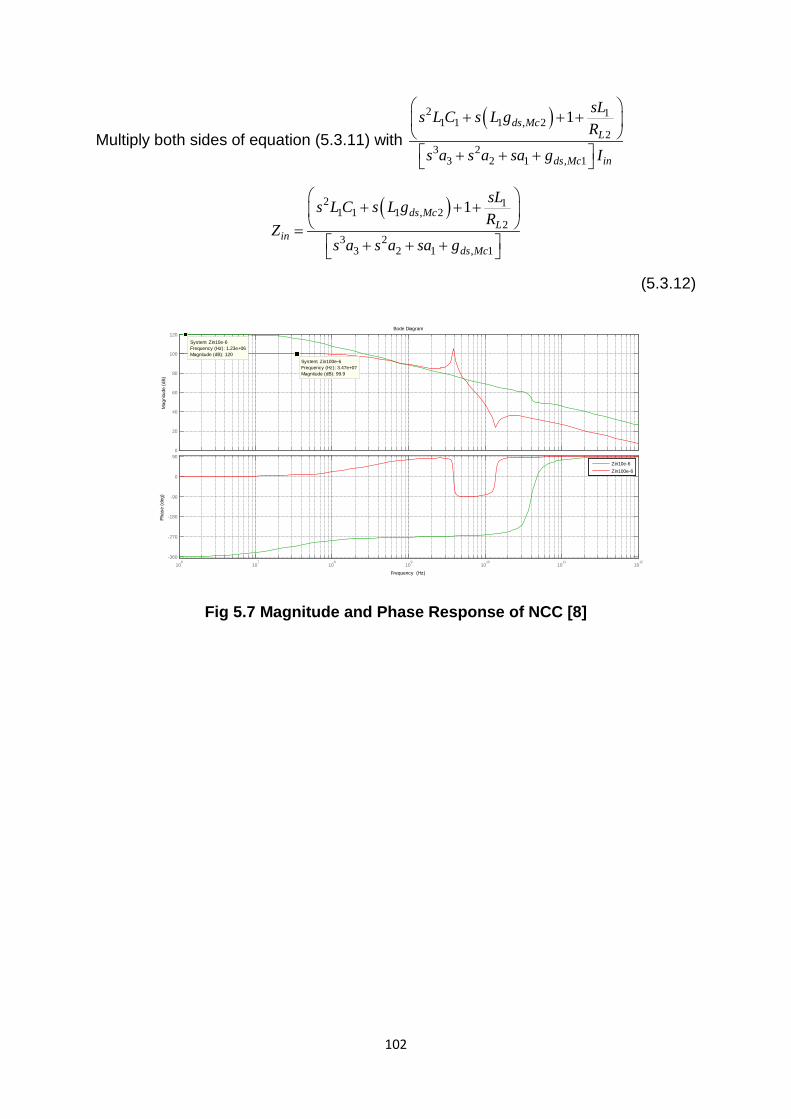
102
Multiply both sides of equation (5.3.11) with ( )2 1
1 1 1 , 22
3 23 2 1 , 1
1ds McL
ds Mc in
sLs L C s L gR
s a s a sa g I
+ + +
+ + +
( )2 11 1 1 , 2
23 2
3 2 1 , 1
1ds McL
inds Mc
sLs L C s L gR
Zs a s a sa g
+ + +
= + + +
(5.3.12)
Fig 5.7 Magnitude and Phase Response of NCC [8]
106
107
108
109
1010
1011
1012
-360
-270
-180
-90
0
90
Phas
e (d
eg)
Bode Diagram
Frequency (Hz)
0
20
40
60
80
100
120System: Zin10e-6Frequency (Hz): 1.23e+06Magnitude (dB): 120
System: Zin100e-6Frequency (Hz): 3.47e+07Magnitude (dB): 99.9
Mag
nitu
de (d
B)
Zin10e-6Zin100e-6
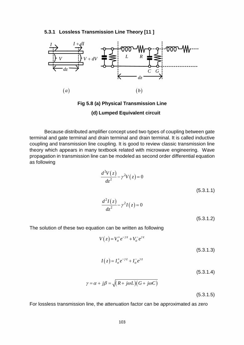
103
5.3.1 Lossless Transmission Line Theory [11 ]
L R
C G
V V dV+
I I dI+
dz
dz
( )a ( )b
Fig 5.8 (a) Physical Transmission Line
(d) Lumped Equivalent circuit
Because distributed amplifier concept used two types of coupling between gate terminal and gate terminal and drain terminal and drain terminal. It is called inductive coupling and transmission line coupling. It is good to review classic transmission line theory which appears in many textbook related with microwave engineering. Wave propagation in transmission line can be modeled as second order differential equation as following
( ) ( )2
22 0
d V zV z
dzγ− =
(5.3.1.1)
( ) ( )2
22 0
d I zI z
dzγ− =
(5.3.1.2)
The solution of these two equation can be written as following
( ) z zo oV z V e V eγ γ+ − −= +
(5.3.1.3)
( ) z zo oI z I e I eγ γ+ − −= +
(5.3.1.4)
( )( )j R j L G j Cγ α β ω ω= + = + +
(5.3.1.5)
For lossless transmission line, the attenuation factor can be approximated as zero
104
Thus, equation 5.3.1.5 can be simplified to
j j LCγ α β ω= + =
(5.3.1.6)
Compare imaginary part with imaginary part in equation (5.3.1.6), phase constant can be written as following
LCβ ω=
(5.3.1.7)
For sinusoidal steady state condition, the differential equation of lumped element or telegrapher equation can be written in phase form as
( ) ( ) ( )dV zR j L I z
dzω= − +
(5.3.1.8)
( ) ( ) ( )dI zG j C V z
dzω= − +
(5.3.1.9)
Differentiate equation (5.3.1.4), it can be written as following
( ) ( ) ( ) ( ) ( ) ( )z z z zo o o o
dI zI e I e I e I e G j C V z
dzγ γ γ γγ γ γ ω+ − − − + − = − + = − = − +
(5.3.1.10)
Differentiate equation (5.3.1.3), it can be written as following
( ) ( ) ( ) ( )( ) ( ) ( )z z z zo o o o
dV zV e V e V e V e R j L I z
dzγ γ γ γγ γ γ ω+ − − − + −= − + = − = − +
(5.3.1.11)
( ) ( ) ( )1 z zo oV e V e I z
R j Lγ γγ
ω+ − −
− = +
(5.3.1.12)
Characteristic impedance can be defined as following
( )( )oR j L R j L R j LZ
G j CR j L G j Cω ω ω
γ ωω ω+ + +
= = =++ +

105
(5.3.1.13)
Table5.2.1 Comparison of Transmission Line waves to uniform plane waves [12]
Transmission Line Uniform Plane Waves 2
22 0d V V
dzγ− =
22
2 0xx
d Ek E
dz+ =
22
2 0d I Idz
γ− = 2
22 0y
yd H
k Hdz
+ =
ZYγ = ˆˆjk zy= z z
o oV V e V eγ γ+ − −= + jkz jkzx o oE E e E e+ − −= +
z zo oI I e I eγ γ+ − −= + jkz jkz
y o oH H e H e+ − −= +
o oo
o o
V V ZZYI I
+ −
+ −= = − = ˆ
ˆo o
o o
E E zyH H
η+ −
+ −= = − =
P VI ∗= z x yS E H ∗=
What is uniform plane waves? Uniform plane waves may travel only in one direction without rotation like circular wave or rectangular waves. Such as electric field propagate into the x direction only and magnetic field propagate into the y direction only. Another meaning of uniform plane waves may have constant amplitude.
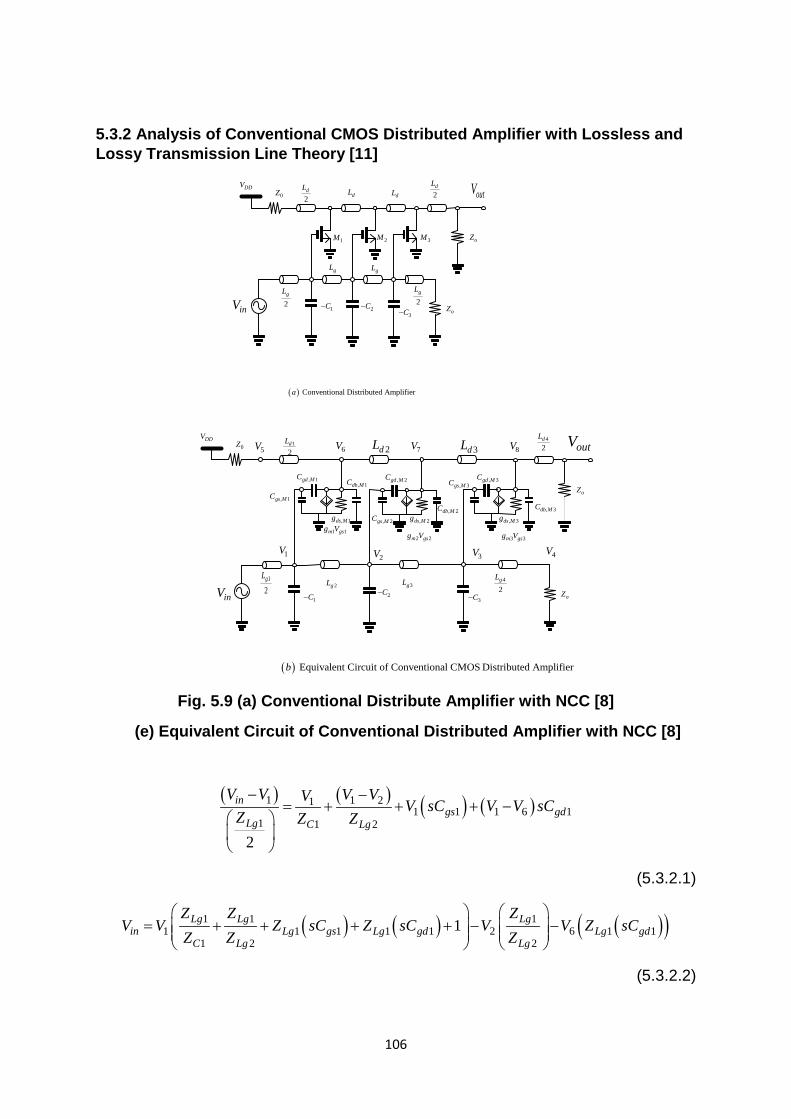
106
5.3.2 Analysis of Conventional CMOS Distributed Amplifier with Lossless and Lossy Transmission Line Theory [11]
2gL
0Z2dL
2dL
dL dL
gL gL
2gL
oZ1M 2M 3M
1C− 2C−3C− oZ
DDVoutV
( ) Conventional Distributed Amplifiera
1
2gL
0Z
oZ
1C− 2C−3C− oZ
DDV
, 1gs MC
, 1gd MC
1 1m gsg V, 2gs MC
2 2m gsg V
, 2gd MC
, 1ds Mg , 2ds Mg, 2db MC
, 1db MC , 3gs MC , 3gd MC
3 3m gsg V
, 3ds Mg, 3db MC
1V2V 3V 4V
5V 6V 7V 8V
( ) Equivalent Circuit of Conventional CMOS Distributed Amplifierb
inV
inV
1
2dL
2dL 3dL 4
2dL
2gL 3gL 4
2gL
outV
Fig. 5.9 (a) Conventional Distribute Amplifier with NCC [8]
(e) Equivalent Circuit of Conventional Distributed Amplifier with NCC [8]
( ) ( ) ( ) ( )1 1 211 1 1 6 1
1 1 2
2
ings gd
Lg C Lg
V V V VV V sC V V sCZ Z Z− −
= + + + −
(5.3.2.1)
( ) ( ) ( )( )1 1 11 1 1 1 1 2 6 1 1
1 2 21Lg Lg Lg
in Lg gs Lg gd Lg gdC Lg Lg
Z Z ZV V Z sC Z sC V V Z sC
Z Z Z
= + + + + − −
(5.3.2.2)
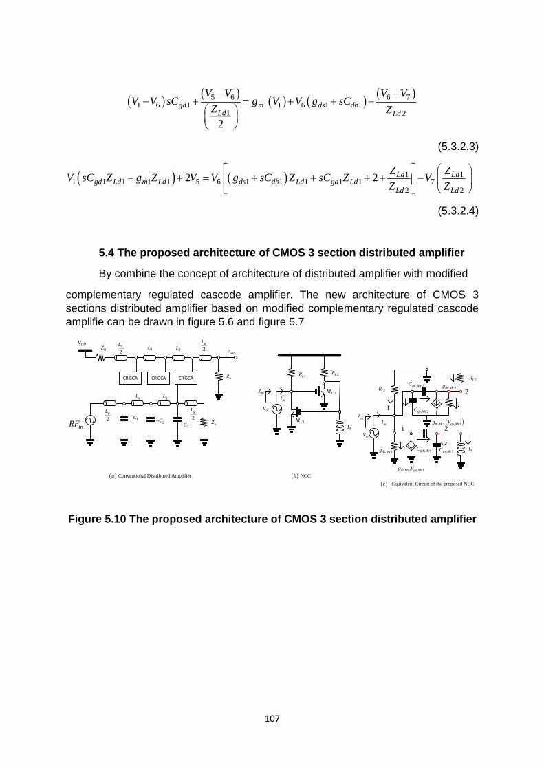
107
( ) ( ) ( ) ( ) ( )5 6 6 71 6 1 1 1 6 1 1
1 22
gd m ds dbLd Ld
V V V VV V sC g V V g sC
Z Z− −
− + = + + +
(5.3.2.3)
( ) ( ) 1 11 1 1 1 1 5 6 1 1 1 1 1 7
2 22 2 Ld Ld
gd Ld m Ld ds db Ld gd LdLd Ld
Z ZV sC Z g Z V V g sC Z sC Z VZ Z
− + = + + + + −
(5.3.2.4)
5.4 The proposed architecture of CMOS 3 section distributed amplifier
By combine the concept of architecture of distributed amplifier with modified
complementary regulated cascode amplifier. The new architecture of CMOS 3 sections distributed amplifier based on modified complementary regulated cascode amplifie can be drawn in figure 5.6 and figure 5.7
inRF 2gL
0Z2dL
2dL
dL dL
gL gL
2gL
oZ
1C−2C−
3C− oZ
DDV
outV
1LR 2LR
inV
inIinZ
1L1CM
2CM
1L
1LR
2LR
inV
inIinZ
, 1gs McC
( ), 1 , 1m Mc gs Mcg V
1
2
2
, 2gd McC, 2ds Mcg
, 1 , 1m Mc gs Mcg V
1
, 1ds Mcg
, 2gs McC
, 1gd McC
( ) Conventional Distributed Amplifiera ( ) NCCb( ) Equivalent Circuit of the proposed NCCc
CRGCA CRGCA CRGCA
Figure 5.10 The proposed architecture of CMOS 3 section distributed amplifier
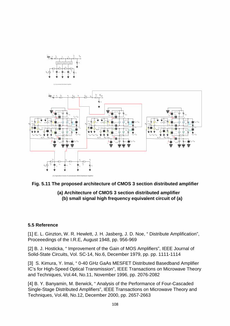
108
2gL
0Z2dL
2dL
dL dL
gL gL
2gL
oZ
1C− 2C−3C− oZ
DDVoutV
( ) Conventional Distributed Amplifiera
0Z
oZ
1C− 2C−3C− oZ
DDV
1V2V 3V 4V
5V 6V 7V8V
( ) Equivalent Circuit of Conventional CMOS Distributed Amplifierb
inV
inV
1
2dL
2dL 3dL 4
2dL
2gL 3gL 4
2gL
outV
1
2gL
CRGCA CRGCA CRGCA
1m ing V
( )2 2 1mg V V−
1dsg
( )4 4 3mg V V−
( )4 30mbg V−
4dsg
( )6 0m ing V −
6dsg
outV
1V
3V 5 6gs dbC C+
3 1gs dbC C+
2 4db dbC C+
3, 2, 7D G D
8 4mg V
4V4V
2V
8 8 5gs db dbC C C+ +
7 2mg V
7 7 3gs db dbC C C+ +
2dsg
( )2 10mbg V−
1 7/ /B dsR g
2 8/ /B dsR g
4 5gs gdC C+
2 3gs gdC C+
2gdC
4gdC
1gdC
1gsC
5 3mg V5dsg
3 1mg V3dsg
6gsC 6gdC
1m ing V
( )2 2 1mg V V−
1dsg
( )4 4 3mg V V−
( )4 30mbg V−
4dsg
( )6 0m ing V −
6dsg
outV
1V
3V
5 6gs dbC C+
3 1gs dbC C+
2 4db dbC C+
3, 2, 7D G D
8 4mg V
4V4V
2V
8 8 5gs db dbC C C+ +
7 2mg V
7 7 3gs db dbC C C+ +
2dsg
( )2 10mbg V−
1 7/ /B dsR g
2 8/ /B dsR g
4 5gs gdC C+
2 3gs gdC C+
2gdC
4gdC
1gdC
1gsC
5 3mg V5dsg
3 1mg V3dsg
6gsC 6gdC
Fig. 5.11 The proposed architecture of CMOS 3 section distributed amplifier
(a) Architecture of CMOS 3 section distributed amplifier (b) small signal high frequency equivalent circuit of (a)
5.5 Reference
[1] E. L. Ginzton, W. R. Hewlett, J. H. Jasberg, J. D. Noe, “ Distribute Amplification”, Proceeedings of the I.R.E, August 1948, pp. 956-969
[2] B. J. Hosticka, “ Improvement of the Gain of MOS Amplifiers”, IEEE Journal of Solid-State Circuits, Vol. SC-14, No.6, December 1979, pp. pp. 1111-1114
[3] S. Kimura, Y. Imai, “ 0-40 GHz GaAs MESFET Distributed Basedband Amplifier IC’s for High-Speed Optical Transmission”, IEEE Transactions on Microwave Theory and Techniques, Vol.44, No.11, November 1996, pp. 2076-2082
[4] B. Y. Banyamin, M. Berwick, “ Analysis of the Performance of Four-Cascaded Single-Stage Distributed Amplifiers”, IEEE Transactions on Microwave Theory and Techniques, Vol.48, No.12, December 2000, pp. 2657-2663
109
[5] R. C. Liu, C. S. Lin, K. L. Deng, H. Wang, “Design and Analysis of DC to 14 GHz and 22 GHz CMOS Cascode Distributed Amplifiers”, IEEE Journal Solid State Circuit, Vol.39, No.8, August 2004, pp. 1370-1374
[6] J. C. Chien, L. H. Lu, “ 40 Gb/s High-Gain Distributed Amplifiers with Cascaded Gain stages in 0.18 um CMOS”, IEEE Journal of Solid-State Circuits, Vol.42, No.12, December 2007, pp. 2715-2725
[7] A. Arbabian, A. M. Niknejad, “ Design of a CMOS Tapered Cascaded Multistage Distributed Amplifier”, IEEE Transactions on Microwave Theory and Techniques, Vol. 57, No.4, April 2009, pp. 938-947
[8] A. Ghadiri, K. Moez, “Gain-Enhanced Distributed Amplifier Using Negative Capacitance”, IEEE Transactions on Circuits and Systems I, Regular Papers, Vol.57, No.11, November 2010, pp. 2834-2843
[9] Y. S. Lin, J. F. Chang, S. S. Lu, “ Analysis and Design of CMOS Distributed Amplifier using Inductively Peaking Cascaded Gain Cell for UWB Systems”, IEEE Transactions on Microwave and Techniquesk, Vol.59, No.10, October 2011, pp. 2513-2524
[10] A. Jahanian, P. Heydari, “ A CMOS Distributed Amplifier with Distributed Active Input Balun Using GBW and Linearity Enhancing Techniques”, IEEE Transactions on Microwave Theory and Techniques, Vol. 60, No.5, May 2012, pp. 1331-1341
[11] D. M. Pozar, “ Microwave Engineering”, 2nd edition, copyright 1998, John Wiley &Sons
[12] R. F. Harrington, “ Time-Harmonic Electromagnetic Fields”, copyright 1961, Mcgraw-Hill, pp.61-63
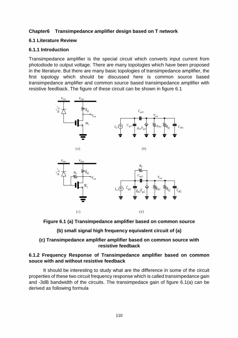
110
Chapter6 Transimpedance amplifier design based on T network
6.1 Literature Review
6.1.1 Introduction
Transimpedance amplifier is the special circuit which converts input current from photodiode to output voltage. There are many topologies which have been proposed in the literature. But there are many basic topologies of transimpedance amplifier, the first topology which should be discussed here is common source based transimpedance amplifier and common source based transimpedance amplifier with resistive feedback. The figure of these circuit can be shown in figure 6.1
PDV DDV
1DRoutV
1MinI 1gsC
1 1m gsg V 1dsg1DR
outV
PDV DDV
2DRoutV
2MinI 2gsC
2 2m gsg V 2dsg2DR
outV1gdCFR
FR
( )a ( )b
( )c ( )d
1dbC
1gdC
2dbC
Figure 6.1 (a) Transimpedance amplifier based on common source
(b) small signal high frequency equivalent circuit of (a)
(c) Transimpedance amplifier amplifier based on common source with resistive feedback
6.1.2 Frequency Response of Transimpedance amplifier based on common souce with and without resistive feedback
It should be interesting to study what are the difference in some of the circuit properties of these two circuit frequency response which is called transimpedance gain and -3dB bandwidth of the circuits. The transimpedace gain of figure 6.1(a) can be derived as following formula
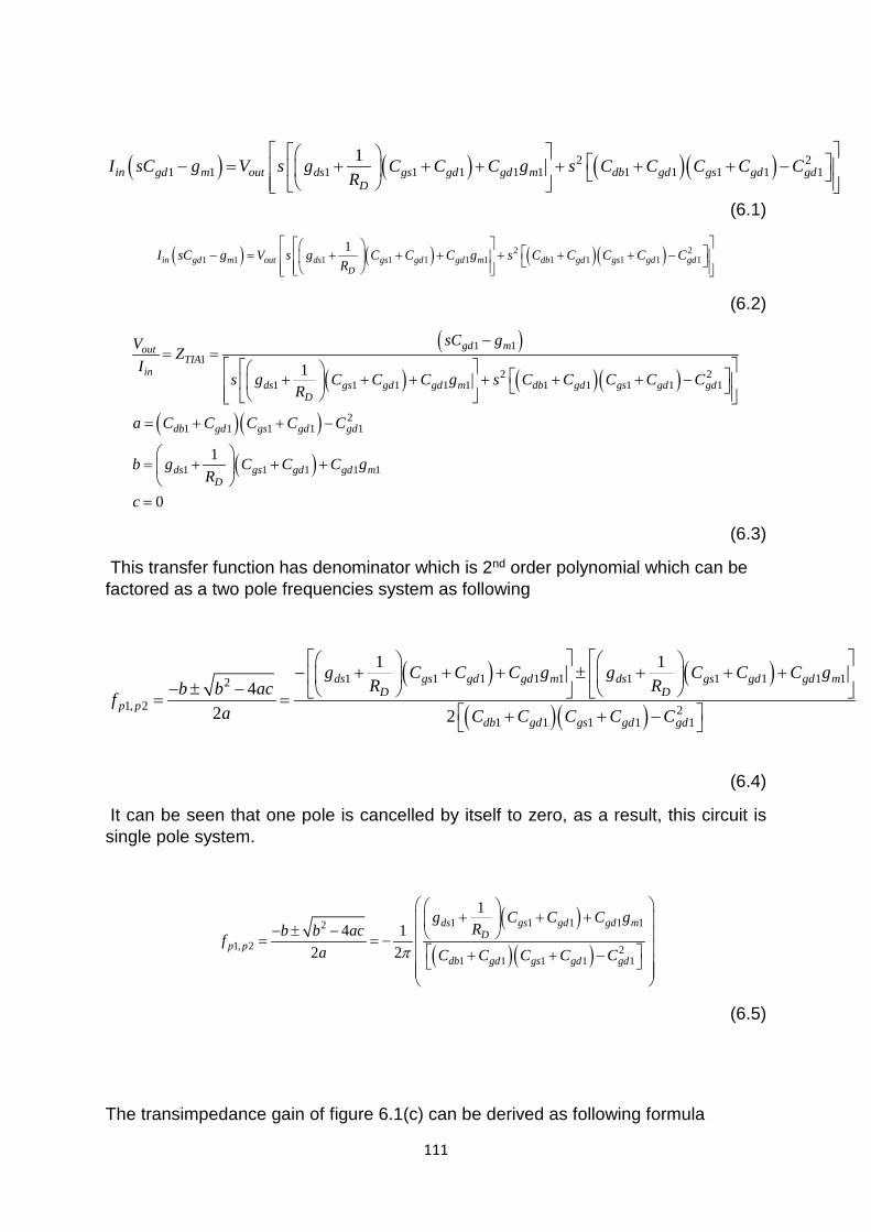
111
( ) ( ) ( )( )2 21 1 1 1 1 1 1 1 1 1 1 1
1in gd m out ds gs gd gd m db gd gs gd gd
DI sC g V s g C C C g s C C C C C
R − = + + + + + + −
(6.1)
( ) ( ) ( )( )2 21 1 1 1 1 1 1 1 1 1 1 1
1in gd m out ds gs gd gd m db gd gs gd gd
DI sC g V s g C C C g s C C C C C
R − = + + + + + + −
(6.2)
( )
( ) ( )( )
( )( )
( )
1 11
2 21 1 1 1 1 1 1 1 1 1
21 1 1 1 1
1 1 1 1 1
1
1
0
gd moutTIA
inds gs gd gd m db gd gs gd gd
D
db gd gs gd gd
ds gs gd gd mD
sC gV ZI
s g C C C g s C C C C CR
a C C C C C
b g C C C gR
c
−= =
+ + + + + + −
= + + −
= + + +
=
(6.3)
This transfer function has denominator which is 2nd order polynomial which can be factored as a two pole frequencies system as following
( ) ( )
( )( )1 1 1 1 1 1 1 1 1 12
1, 2 21 1 1 1 1
1 14
2 2
ds gs gd gd m ds gs gd gd mD D
p pdb gd gs gd gd
g C C C g g C C C gR Rb b acf
a C C C C C
− + + + ± + + +
− ± − = = + + −
(6.4)
It can be seen that one pole is cancelled by itself to zero, as a result, this circuit is single pole system.
( )( )( )
1 1 1 1 12
1, 2 21 1 1 1 1
14 1
2 2
ds gs gd gd mD
p pdb gd gs gd gd
g C C C gRb b acf
a C C C C Cπ
+ + +
− ± − = = − + + −
(6.5)
The transimpedance gain of figure 6.1(c) can be derived as following formula
112
( )( ) ( ) ( )1 121 1 1 1 1 1 1
12 21 11 1 1
11
1 1
1 1 1
gs gddb gd gs gd gs gd ds
D F F
gdin gd m outgd gd m
Fds
D F F m
F
C Cs C C C C s C C g
R R R
CI sC g V s C s C gR
gR R R g
R
+ + + + + + + + − = + −
+ + + − −
(6.6)
( )
( ) ( )
1 12 2 2 2
1 1 1 1 1 1 1 1
1 11 1 1 1 1 1
1 1 1 1 1 1
1
1 1 1 1 1
gd moutTIA
in db gs db gd gd gs gd gd
gs mgs gd ds gd m ds
D F F D F F F
db gs db gd gd gs
gs
sC gVZ
I s C C C C C C C C
C gs C C g C g gR R R R R R R
a C C C C C C
b C
− = = + + + − + + + + + + + + + +
= + +
= +( ) ( )11 1 1 1
11
1 1
1 1 1
gsgd ds gd m
D F F
mds
D F F F
CC g C g
R R R
gc g
R R R R
+ + + +
= + + +
(6.7)
It can be seen that this transimpedance gain has denominator which is 2nd order polynomial which can be factored as a two pole frequencies system as following
( ) ( )
( ) ( )
( )
11 1 1 1 1
21
1 1 1 1 1
11 1 1 1 1 1 12
1, 2
1 1
1 1
1 1 144 1
2 2
gsgs gd ds gd m
D F F
gsgs gd ds gd m
D F F
mdb gs db gd gd gs ds
D F F Fp p
CC C g C g
R R R
CC C g C g
R R R
gC C C C C C gR R R Rb b acf
a π
− + + + + + ±
+ + + + +
− + + + + + − ± − = = ( )1 1 1 1 1 12 db gs db gd gd gsC C C C C C+ +
(6.8)
113
Figure 6.2 Magnitude and Phase Response of Transimpedance amplifier
In figure 6.1(a), 6.1(c) @ 10 microampere
Table 6.1 Circuit parameters from Simulation Results from figure 6.1 (a), 6.1 (c)
Aspect Ratio=17.06 1 2 4.72gs gsC C fF= = 101 1.02 10paω = − ×
1 21ds dsg gµ= Ω = 1 2 1.68gd gdC C fF= = 111 1.4167 10zaω = ×
1 25.80n nW um W= = 1 2 5.57db dbC C fF= = ( ) 111, 2 0.0768 7.8962 10pb pb iω = − ± ×
1 2 2.387m mg g µ= = 1 2 160D DR R k= = Ω 111 1.4167 10zbω = ×
, 1 , 210D M D MI A Iµ= = 5FR k= Ω
6.1.3 Frequency response of Transimpedance amplifier with and without resistive feedback with parasitic of photo diode and resistive bias circuit
It is well known that photodiode has parasitic capacitance in the range of several hundred femtofarad to several picofarad which depend on the speed of the photodiode. This section will discuss what is the effect of parasitic capacitance of photo diode and resistive bias circuit.
0
50
100
150
System: sys2Frequency (Hz): 2.05e+08Magnitude (dB): 18.9
System: sysFrequency (Hz): 1.01e+10Magnitude (dB): 63.3
System: sys2Frequency (Hz): 1.25e+11Magnitude (dB): 66.9
Mag
nitu
de (d
B)
107
108
109
1010
1011
1012
-90
-45
0
45
90
135
180
Phas
e (d
eg)
Bode Diagram
Frequency (Hz)
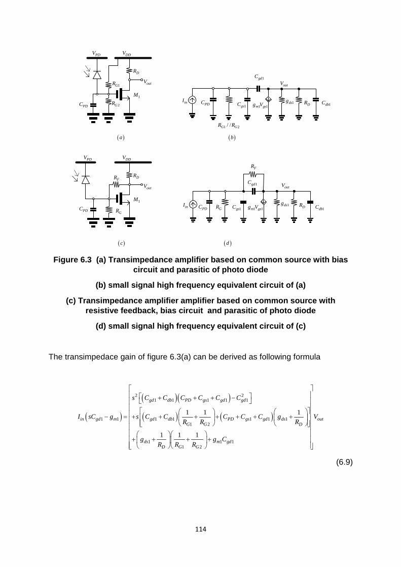
114
PDV DDV
DR
outV
1MinI
1gsC 1 1m gsg V 1dsgDR
outV
PDV DDV
DR
outV
1MinI
1gsC 1 1m gsg V 1dsgDR
outV1gdCFR
FR
( )a ( )b
( )c ( )d
1dbC
1gdC
1dbCGRPDC PDC GR
1GR
2GR PDC
1 2/ /G GR R
PDC
Figure 6.3 (a) Transimpedance amplifier based on common source with bias
circuit and parasitic of photo diode
(b) small signal high frequency equivalent circuit of (a)
(c) Transimpedance amplifier amplifier based on common source with resistive feedback, bias circuit and parasitic of photo diode
(d) small signal high frequency equivalent circuit of (c)
The transimpedace gain of figure 6.3(a) can be derived as following formula
( )
( )( )
( ) ( )
2 21 1 1 1 1
1 1 1 1 1 1 11 2
1 1 11 2
1 1 1
1 1 1
gd db PD gs gd gd
in gd m gd db PD gs gd ds outG G D
ds m gdD G G
s C C C C C C
I sC g s C C C C C g VR R R
g g CR R R
+ + + − − = + + + + + + + + + + +
(6.9)
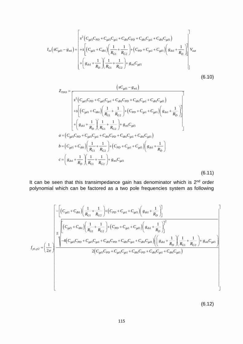
115
( )
( )
( ) ( )
21 1 1 1 1 1 1 1
1 1 1 1 1 1 11 2
1 1 11 2
1 1 1
1 1 1
gd PD gd gs db PD db gs db gd
in gd m gd db PD gs gd ds outG G D
ds m gdD G G
s C C C C C C C C C C
I sC g s C C C C C g VR R R
g g CR R R
+ + + + − = + + + + + + + + + + +
(6.10)
( )
( )
( ) ( )
1 13
21 1 1 1 1 1 1 1
1 1 1 1 11 2
1 1 11 2
1 1 1 1
1 1 1
1 1 1
gd mTIA
gd PD gd gs db PD db gs db gd
gd db PD gs gd dsG G D
ds m gdD G G
gd PD gd gs db
sC gZ
s C C C C C C C C C C
s C C C C C gR R R
g g CR R R
a C C C C C
−= + + + + + + + + + + + + + + +
= + +( )
( ) ( )
1 1 1 1
1 1 1 1 11 2
1 1 11 2
1 1 1
1 1 1
PD db gs db gd
gd db PD gs gd dsG G D
ds m gdD G G
C C C C C
b C C C C C gR R R
c g g CR R R
+ +
= + + + + + +
= + + +
(6.11)
It can be seen that this transimpedance gain has denominator which is 2nd order polynomial which can be factored as a two pole frequencies system as following
( ) ( )
( ) ( )
( )
1 1 1 1 11 2
2
1 1 1 1 11 2
1 1 1 1 1 1 1 1 11
1, 2
1 1 1
1 1 1
1 1 141
2
gd db PD gs gd dsG G D
gd db PD gs gd dsG G D
gd PD gd gs db PD db gs db gd dsD G
p p
C C C C C gR R R
C C C C C gR R R
C C C C C C C C C C gR R R
fπ
− + + + + + +
+ + + + + +
±
− + + + + + + =
( )1 1
2
1 1 1 1 1 1 1 12
m gdG
gd PD gd gs db PD db gs db gd
g C
C C C C C C C C C C
+ + + + +
(6.12)
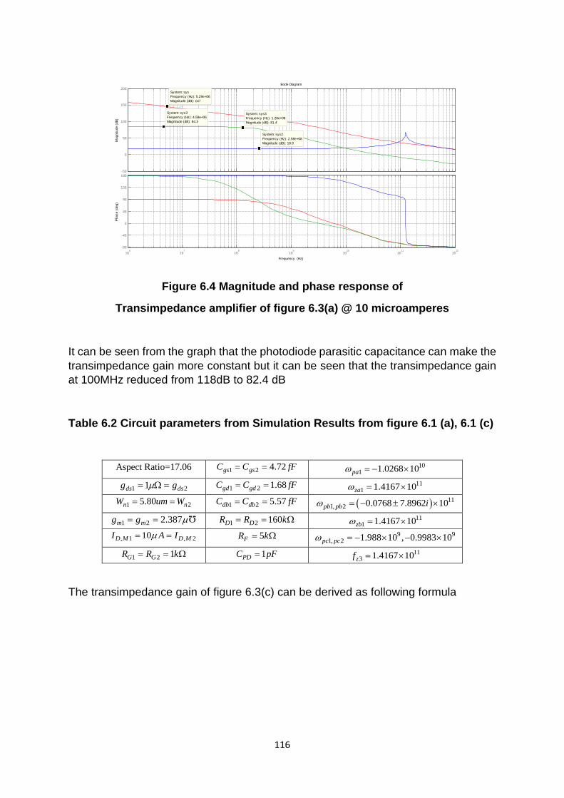
116
Figure 6.4 Magnitude and phase response of
Transimpedance amplifier of figure 6.3(a) @ 10 microamperes
It can be seen from the graph that the photodiode parasitic capacitance can make the transimpedance gain more constant but it can be seen that the transimpedance gain at 100MHz reduced from 118dB to 82.4 dB
Table 6.2 Circuit parameters from Simulation Results from figure 6.1 (a), 6.1 (c)
Aspect Ratio=17.06 1 2 4.72gs gsC C fF= = 101 1.0268 10paω = − ×
1 21ds dsg gµ= Ω = 1 2 1.68gd gdC C fF= = 111 1.4167 10zaω = ×
1 25.80n nW um W= = 1 2 5.57db dbC C fF= = ( ) 111, 2 0.0768 7.8962 10pb pb iω = − ± ×
1 2 2.387m mg g µ= = 1 2 160D DR R k= = Ω 111 1.4167 10zbω = ×
, 1 , 210D M D MI A Iµ= = 5FR k= Ω 9 91, 2 1.988 10 , 0.9983 10pc pcω = − × − ×
1 2 1G GR R k= = Ω 1PDC pF= 113 1.4167 10zf = ×
The transimpedance gain of figure 6.3(c) can be derived as following formula
-50
0
50
100
150
200
System: sys3Frequency (Hz): 4.58e+06Magnitude (dB): 84.3
System: sysFrequency (Hz): 5.29e+06Magnitude (dB): 147
System: sys2Frequency (Hz): 2.58e+08Magnitude (dB): 18.9
System: sys3Frequency (Hz): 1.28e+08Magnitude (dB): 81.4
Mag
nitu
de (d
B)
106
107
108
109
1010
1011
1012
-90
-45
0
45
90
135
180
Phas
e (d
eg)
Bode Diagram
Frequency (Hz)
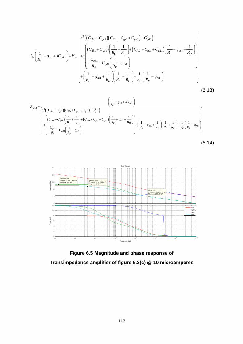
117
( )( )( )( ) ( )
2 21 1 1 1 1
1 1 1 1 1
1 11
1 1
1 1
1 1 1 11
1
1 1 1 1 1 1
db gd PD gs gd gd
db gd PD gs gd dsG F F D
in m gd outF gd
gd mF F
ds mF D G F F F
s C C C C C C
C C C C C gR R R R
I g sC V sR C
C gR R
g gR R R R R R
+ + + −
+ + + + + + +
− + = + − − −
+ + + + − −
(6.13)
( )( )( )( ) ( )
1 1
4 2 21 1 1 1 1
1 1 1 1 1
1 11
1 1
1
1 1 1 11 1 1 1 1 1
1
m gdF
TIAdb gd PD gs gd gd
db gd PD gs gd dsG F F D
ds mF D G F F Fgd
gd mF F
g sCR
Zs C C C C C C
C C C C C gR R R R
s g gR R R R R RC
C gR R
− +
= + + + −
+ + + + + + +
+ + + + + − − − − −
(6.14)
Figure 6.5 Magnitude and phase response of
Transimpedance amplifier of figure 6.3(c) @ 10 microamperes
106
107
108
109
1010
1011
1012
1013
-90
-45
0
45
90
135
180
Phas
e (d
eg)
Bode Diagram
Frequency (Hz)
-50
0
50
100
150
200
System: sys3Frequency (Hz): 1.46e+06Magnitude (dB): 82.1
System: sys7Frequency (Hz): 4.26e+07Magnitude (dB): 71.1
System: sys7Frequency (Hz): 3.69e+10Magnitude (dB): 0.457
Mag
nitu
de (d
B)
syssys2sys3sys7
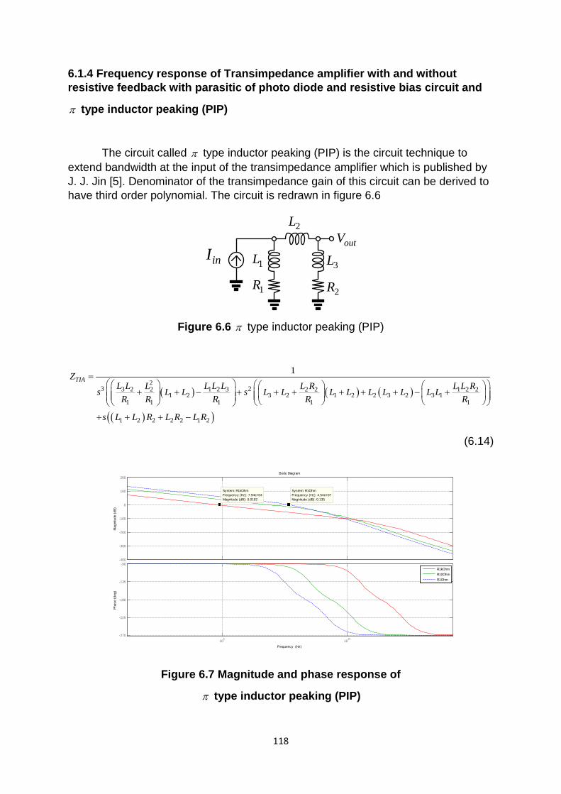
118
6.1.4 Frequency response of Transimpedance amplifier with and without resistive feedback with parasitic of photo diode and resistive bias circuit and
π type inductor peaking (PIP)
The circuit called π type inductor peaking (PIP) is the circuit technique to extend bandwidth at the input of the transimpedance amplifier which is published by J. J. Jin [5]. Denominator of the transimpedance gain of this circuit can be derived to have third order polynomial. The circuit is redrawn in figure 6.6
inI1L
2L
3L
1R 2R
outV
Figure 6.6 π type inductor peaking (PIP)
( ) ( ) ( )
( )( )
23 23 2 1 2 32 2 2 1 2 2
1 2 3 2 1 2 2 3 2 3 11 1 1 1 1
1 2 2 2 2 1 2
1TIAZ
L L L L LL L R L L Rs L L s L L L L L L L L LR R R R R
s L L R L R L R
=
+ + − + + + + + + − + + + + −
(6.14)
Figure 6.7 Magnitude and phase response of
π type inductor peaking (PIP)
105
1010
-270
-225
-180
-135
-90
Phas
e (d
eg)
Bode Diagram
Frequency (Hz)
-400
-300
-200
-100
0
100
200
System: R1kOhmFrequency (Hz): 7.94e+04Magnitude (dB): 0.0182
System: R1OhmFrequency (Hz): 4.54e+07Magnitude (dB): 0.135
Mag
nitu
de (d
B)
R1kOhmR10OhmR1Ohm
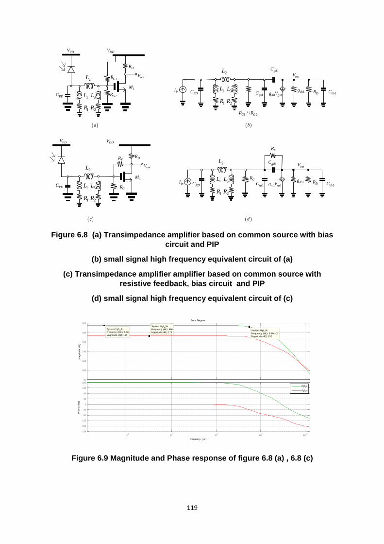
119
PDV DDV
DR
outV
1MinI
1gsC 1 1m gsg V 1dsgDR
outV
PDV DDV
DR
outV
1MinI
1gsC 1 1m gsg V 1dsgDR
outV1gdCFR
FR
( )a ( )b
( )c ( )d
1dbC
1gdC
1dbCGRPDC PDC
GR
1GR
2GR PDC
1 2/ /G GR R
PDC 1L
2L
3L
1R 2R
1L
2L
3L
1R 2R
1L
2L
3L
1R 2R
1L
2L
3L
1R 2R
Figure 6.8 (a) Transimpedance amplifier based on common source with bias
circuit and PIP
(b) small signal high frequency equivalent circuit of (a)
(c) Transimpedance amplifier amplifier based on common source with resistive feedback, bias circuit and PIP
(d) small signal high frequency equivalent circuit of (c)
Figure 6.9 Magnitude and Phase response of figure 6.8 (a) , 6.8 (c)
102
104
106
108
1010
-225
-180
-135
-90
-45
0
45
90
135
180
Phas
e (d
eg)
Bode Diagram
Frequency (Hz)
80
100
120
140
160
180
200
System: f ig6_8cFrequency (Hz): 9.78Magnitude (dB): 195
System: f ig6_8aFrequency (Hz): 996Magnitude (dB): 173
System: f ig6_8cFrequency (Hz): 3.04e+07Magnitude (dB): 192
Mag
nitu
de (d
B)
f ig68c
fig68a
120
Usually, it is based on cascade common source amplifier. Kim [8] proposed series silicon inductor between input terminal and gate terminal of the transistor.
Input1 485L pH=
1 1R k= Ω2 65R = Ω
195FR = ΩBIASI
DDV
1M 2M
2 165L pH=
3 210L pH=3M
3 65R = Ω4M
4 365L pH=
5 565L pH=BIASV
Fig 6.10 Common source transimpedance amplifier with resistive feedback and inductive degeneration at gate terminal [8]
121
6.1.5 Equivalent input noise voltage response of Transimpedance amplier
There are two types of noise in CMOS technology. The first type is flicker noise which is dominant at low frequency. The second type is thermal noise which is constant as a function of frequency. The flicker noise voltage mean square equation can be rewritten here [2]
2, ker
1n flic
ox
KVC WL f
=
(6.1.4.1)
K is a process dependent constant, f is input frequency, Cox is oxide capacitance of the CMOS process. The flicker noise current mean square can be rewritten here
2 2, ker
1n fli m
ox
KI gC WL f
=
(6.1.4.2)
The thermal noise voltage mean square can be rewritten here as following
2 4n mV kT gγ=
(6.1.4.3)
The thermal noise current mean square can be rewritten here as following
2,
843n thermal m mI kT g kTgγ= =
(6.1.4.4)

122
PDV DDV
outV
1M
PDV DDV
outVFR
( )a ( )b
( )c ( )d
2DR
2M
1DR
DDV
1M
1DR
ac
1
2, Dn RI
1
2,n MI
DDV
FR2DR
2Mac
2
2, Dn RI
2
2,n MI
2, Fn RI
Figure 6.11 (a) Transimpedance amplifier based on common source
(b) Mean squared noise current source of (a)
(c) Transimpedance amplifier amplifier based on common source with resistive feedback
(d) Mean squared noise current source of (c)
123
Table 6.5 Performance Comparison of TIA with different technology Ref Process BW
( )GHz ( )TZ dBΩ GD
(psec) Noise
/pA Hz Supply
(V) Power (mW)
Area
( 2mm )
Figure of Merit
[4] 0.18mµ
9.2 54 2.5 137.5 0.64
[5] 0.18mµ
30.5 51 55.7 1.8 60.1 1.17 0.46×
[6] 0.18mµ
4.3 54.5 1.5 11.5 0.0077
[7] 0.18mµ
6.2-10.5
47.8 1.8 33.3 0.9 0.6×
[8] 0.13mµ
29
50 16 51.8 1.5 45.7 0.4
[10] 65 nm 46.7 30 39.9 [11] 0.18
mµ 8
@ 0.25pF 53 20± 18 1.8 13.5 0.45 0.25×
[12] 0.18mµ
7 @ 0.2 pF
55 65 10± 17.5 1.8 18.6 0.45 0.25×
6.5 References
[1] E. Sackinger, “ Broadband Circuits for Optical Fiber Communication”, John Wiley & Sons, copyright 2005
[2] B. Razavi, “ RF Microelectronics”, Second edition, Prentic-Hall, copyright 2012
[3] A. A. Abidi, “Gigahertz Transresistance Amplifiers in Fine Line NMOS”, IEEE Journal of Solid-State Circuits, Vol. SC-19, No.6, December 1984, pp. 986-994
[4] B. Analui, A. Hajimari, “ Bandwidth Enhancement for Transimpedance Amplifier”, IEEE Journal of Solid-State Circuits, Vol.39, No.8, August 2004, pp. 1263-1270
[5] J. D. Jin, S. S. H. Hsu, “ A 40 Gb/s Transimpedance Amplifier in 0.18 um CMOS Technology”, IEEE Journal of Solid State Cricut, Vol.43, No.6, June 2008, pp. 1449-1457
[6] S. S. H. Hsu, W. H. Cho, S. W. Chen, J. D. Jin, “ CMOS Broadband amplifiers for Optical Communicatinos and Optical Interconnects”, RFIT2011, pp. 105-108
[7] C. K. Chien, H. H. Hsieh, H. S. Chen, L. H. Lu, “ A Transimpedance Amplifier with a tunable bandwidth in 0.18 um CMOS”, IEEE Transactions on Microwave Theory and Techniques, Vol.58, No.3, March 2010, pp. 498-505
124
[8] J. Kim, J. F. Buckwalter, “ Bandwidth Enhancement with low group delay variation for a 40 Gb/s Transimpedance amplifier”, IEEE Transactions on Circuits and Systems- I, Regular papers, Vol.57, No.8, August 2010, pp. 1964-1972
[9] S.H. Huang, W.Z. Chen, Y.W. Chang, Y.T Huang, “A 10 Gb/s OEIC with Meshed Spatially-Modulated Photo Detector in 0.18 um CMOS Technology”, IEEE Journal of Solid-State Circuit, Vol.46, No.5, May 2011, pp. 1158-1169
[10] S. Bashiri, C. Plett, J. Aguirre, P. Schvan, “A 40 Gb/s Transimpedance Amplifier in 65 nm CMOS”, pp.757-760
[11] Z. Lu, K. S. Yeo, J. Ma, M. A. Do, W. M. Lim, X. Chen, “ Broadband design techniques for Transimpedance Amplifier”, IEEE Transactions on Circuit and Systems, I Regular Papers, Vol.54, No.3, March 2007, pp. 590-600
[12] Z. Lu, K. S. Yeo, W. M. Lim, M. A. Do, C. C. Boon, “Design of a CMOS Broadband Transimpedance Amplifier with Active Feedback”, IEEE Transactions on Very Large Scale Integration (VLSI) Systems”, Vol.18, No.3, March 2010, pp. 461-472
Related Documents