TMS320C6000 Technical Brief Literature Number: SPRU197D February 1999 Printed on Recycled Paper

Welcome message from author
This document is posted to help you gain knowledge. Please leave a comment to let me know what you think about it! Share it to your friends and learn new things together.
Transcript

TMS320C6000Technical Brief
Literature Number: SPRU197DFebruary 1999
Printed on Recycled Paper

IMPORTANT NOTICE
Texas Instruments and its subsidiaries (TI) reserve the right to make changes to their productsor to discontinue any product or service without notice, and advise customers to obtain the latestversion of relevant information to verify, before placing orders, that information being relied onis current and complete. All products are sold subject to the terms and conditions of sale suppliedat the time of order acknowledgement, including those pertaining to warranty, patentinfringement, and limitation of liability.
TI warrants performance of its semiconductor products to the specifications applicable at thetime of sale in accordance with TI’s standard warranty. Testing and other quality controltechniques are utilized to the extent TI deems necessary to support this warranty. Specific testingof all parameters of each device is not necessarily performed, except those mandated bygovernment requirements.
CERTAIN APPLICATIONS USING SEMICONDUCTOR PRODUCTS MAY INVOLVEPOTENTIAL RISKS OF DEATH, PERSONAL INJURY, OR SEVERE PROPERTY ORENVIRONMENTAL DAMAGE (“CRITICAL APPLICATIONS”). TI SEMICONDUCTORPRODUCTS ARE NOT DESIGNED, AUTHORIZED, OR WARRANTED TO BE SUITABLE FORUSE IN LIFE-SUPPORT DEVICES OR SYSTEMS OR OTHER CRITICAL APPLICATIONS.INCLUSION OF TI PRODUCTS IN SUCH APPLICATIONS IS UNDERSTOOD TO BE FULLYAT THE CUSTOMER’S RISK.
In order to minimize risks associated with the customer’s applications, adequate design andoperating safeguards must be provided by the customer to minimize inherent or proceduralhazards.
TI assumes no liability for applications assistance or customer product design. TI does notwarrant or represent that any license, either express or implied, is granted under any patent right,copyright, mask work right, or other intellectual property right of TI covering or relating to anycombination, machine, or process in which such semiconductor products or services might beor are used. TI’s publication of information regarding any third party’s products or services doesnot constitute TI’s approval, warranty or endorsement thereof.
Copyright 1999, Texas Instruments Incorporated
iiiRead This First
Preface
Read This First
About This Manual
This book is an introduction to the TMS320C6000 platform of digital signalprocessor (DSP) devices. This book describes the CPU architecture, periph-erals, and development tools for the TMS320C6000 DSPs. Unless otherwisespecified, all references to the ’C6000 refer to the TMS320C6000 platform ofDSPs, ’C62x refers to the TMS320C62x fixed-point DSPs in the ’C6000 plat-form, and ’C67x refers to the TMS320C67x floating-point DSPs in the ’C6000platform.
How to Use This Manual
The following table summarizes the information in this technical brief:
If you are looking forinformation about: Turn to these chapters:
Code generation tools Chapter 5, Development Support
CPU architecture Chapter 2, CPU Architecture
Development support tools Chapter 5, Development Support
Direct-memory access (DMA) Chapter 4, Peripherals
Evaluation tools Chapter 5, Development Support
External memory interface Chapter 3, Memory
Chapter 4, Peripherals
Host-port interface Chapter 4, Peripherals
Memory map Chapter 3, Memory
Multichannel buffered serialport (McBSP)
Chapter 4, Peripherals
Peripherals Chapter 4, Peripherals
Timers Chapter 4, Peripherals
Related Documentation From Texas Instruments
iv
Related Documentation From Texas Instruments
The following books describe the TMS320C62x/C67x devices and relatedsupport tools. To obtain a copy of any of these TI documents, call the TexasInstruments Literature Response Center at (800) 477–8924. When ordering,please identify the book by its title and literature number.
TMS320C6201 Digital Signal Processor Data Sheet (literature numberSPRS051) describes the features of the TMS320C6201 and providespinouts, electrical specifications, and timings for the device.
TMS320C6202 Digital Signal Processor Data Sheet (literature numberSPRS072) describes the features of the TMS320C6202 and providespinouts, electrical specifications, and timings for the device.
TMS320C6211 Digital Signal Processor Data Sheet (literature numberSPRS073) describes the features of the TMS320C6211 and providespinouts, electrical specifications, and timings for the device.
TMS320C6701 Digital Signal Processor Data Sheet (literature numberSPRS067) describes the features of the TMS320C6701 and providespinouts, electrical specifications, and timings for the device.
TMS320C62x/C67x CPU and Instruction Set Reference Guide (literaturenumber SPRU189) describes the ’C62x/C67x CPU architecture, instruc-tion set, pipeline, and interrupts for these digital signal processors.
TMS320C6201/C6701 Peripherals Reference Guide (literature numberSPRU190) describes common peripherals available on theTMS320C6201/C6701 digital signal processors. This book includes in-formation on the internal data and program memories, the externalmemory interface (EMIF), the host port, multichannel buffered serialports, direct memory access (DMA), clocking and phase-locked loop(PLL), and the power-down modes.
TMS320C6202/C6211 Peripheral Addendum to the TMS320C6201/C6701Peripherals Reference Guide (literature number SPRU290) describescommon peripherals available on the TMS320C6202/C6211 digitalsignal processors. This book includes information on the internal dataand program memories, the external memory interface (EMIF), the hostport, multichannel buffered serial ports, direct memory access (DMA),clocking and phase-locked loop (PLL), and the power-down modes.
TMS320C62x/C67x Programmer’s Guide (literature number SPRU198)describes ways to optimize C and assembly code for theTMS320C62x/C67x DSPs and includes application program examples.
vRead This First
TMS320C6x Assembly Language Tools User’s Guide (literature numberSPRU186) describes the assembly language tools (assembler, linker,and other tools used to develop assembly language code), assemblerdirectives, macros, common object file format, and symbolic debuggingdirectives for the ’C6x generation of devices.
TMS320C6x Optimizing C Compiler User’s Guide (literature numberSPRU187) describes the ’C6x C compiler and the assembly optimizer.This C compiler accepts ANSI standard C source code and produces as-sembly language source code for the ’C6x generation of devices. The as-sembly optimizer helps you optimize your assembly code.
TMS320C6x C Source Debugger User’s Guide (literature numberSPRU188) tells you how to invoke the ’C6x simulator and emulatorversions of the C source debugger interface. This book discussesvarious aspects of the debugger, including command entry, codeexecution, data management, breakpoints, profiling, and analysis.
TMS320 DSP Development Support Reference Guide (literature numberSPRU011) describes the TMS320 family of digital signal processors andthe tools that support these devices. Included are code-generation tools(compilers, assemblers, linkers, etc.) and system integration and debugtools (simulators, emulators, evaluation modules, etc.). Also covered areavailable documentation, seminars, the university program, and factoryrepair and exchange.
Trademarks
Classico, MicroLite, and Virtuoso Nano are trademarks of Eonic Systems, Inc.
Code Composer and Code Maestro are trademarks of GO DSP Corporation.
EVP is a trademark of D2 Technologies.
InvisiLink is a trademark of ViaDSP, Inc.
PC is a trademark of International Business Machines Corporation.
Solaris, SunOS, and Sun-3 are trademarks of Sun Microsystems, Inc.
SPI is a trademark of Motorola, Inc.
320 Hotline On-line, TI, VelociTI, XDS510, and XDS510WS are trademarks ofTexas Instruments Incorporated.
Windows and Windows NT are registered trademarks of MicrosoftCorporation.
Related Documentation From Texas Instruments / Trademarks

If You Need Assistance
vi
If You Need Assistance . . .
� World-Wide Web SitesTI Online http://www.ti.comSemiconductor Product Information Center (PIC) http://www.ti.com/sc/docs/pic/home.htmDSP Solutions http://www.ti.com/dsps320 Hotline On-line� http://www.ti.com/sc/docs/dsps/support.htm
� North America, South America, Central AmericaProduct Information Center (PIC) (972) 644-5580TI Literature Response Center U.S.A. (800) 477-8924Software Registration/Upgrades (214) 638-0333 Fax: (214) 638-7742U.S.A. Factory Repair/Hardware Upgrades (281) 274-2285U.S. Technical Training Organization (972) 644-5580DSP Hotline (281) 274-2320 Fax: (281) 274-2324 Email: [email protected] Modem BBS (281) 274-2323DSP Internet BBS via anonymous ftp to ftp://ftp.ti.com/pub/tms320bbs
� Europe, Middle East, AfricaEuropean Product Information Center (EPIC) Hotlines:
Multi-Language Support +33 1 30 70 11 69 Fax: +33 1 30 70 10 32Email: [email protected]
Deutsch +49 8161 80 33 11 or +33 1 30 70 11 68English +33 1 30 70 11 65Francais +33 1 30 70 11 64Italiano +33 1 30 70 11 67
EPIC Modem BBS +33 1 30 70 11 99European Factory Repair +33 4 93 22 25 40Europe Customer Training Helpline Fax: +49 81 61 80 40 10
� Asia-PacificLiterature Response Center +852 2 956 7288 Fax: +852 2 956 2200Hong Kong DSP Hotline +852 2 956 7268 Fax: +852 2 956 1002Korea DSP Hotline +82 2 551 2804 Fax: +82 2 551 2828Korea DSP Modem BBS +82 2 551 2914Singapore DSP Hotline Fax: +65 390 7179Taiwan DSP Hotline +886 2 377 1450 Fax: +886 2 377 2718Taiwan DSP Modem BBS +886 2 376 2592Taiwan DSP Internet BBS via anonymous ftp to ftp://dsp.ee.tit.edu.tw/pub/TI/
� JapanProduct Information Center +0120-81-0026 (in Japan) Fax: +0120-81-0036 (in Japan)
+03-3457-0972 or (INTL) 813-3457-0972 Fax: +03-3457-1259 or (INTL) 813-3457-1259DSP Hotline +03-3769-8735 or (INTL) 813-3769-8735 Fax: +03-3457-7071 or (INTL) 813-3457-7071DSP BBS via Nifty-Serve Type “Go TIASP”
� DocumentationWhen making suggestions or reporting errors in documentation, please include the following information that is on the titlepage: the full title of the book, the publication date, and the literature number.
Mail: Texas Instruments Incorporated Email: [email protected] Documentation Services, MS 702P.O. Box 1443Houston, Texas 77251-1443
Note: When calling a Literature Response Center to order documentation, please specify the literature number of thebook.
Contents
vii
Contents
1 Introduction 1�1. . . . . . . . . . . . . . . . . . . . . . . . . . . . . . . . . . . . . . . . . . . . . . . . . . . . . . . . . . . . . . . . . . . . . Describes the main features of the TMS320C62x/C67x devices, the history of TI DSPs, andtypical applications.
1.1 The TMS320 Family of Digital Signal Processors 1�2. . . . . . . . . . . . . . . . . . . . . . . . . . . . . . . 1.1.1 History, Development, and Advantages of TMS320 DSPs 1�2. . . . . . . . . . . . . . . . . 1.1.2 Typical Applications for the TMS320 Family 1�3. . . . . . . . . . . . . . . . . . . . . . . . . . . . .
1.2 Introduction to the TMS320C6000 Platform of Digital Signal Processors 1�5. . . . . . . . . . . 1.3 Features and Options of the TMS320C62x/C67x Devices 1�6. . . . . . . . . . . . . . . . . . . . . . . .
2 CPU Architecture 2�1. . . . . . . . . . . . . . . . . . . . . . . . . . . . . . . . . . . . . . . . . . . . . . . . . . . . . . . . . . . . . . . . Describes the CPU architecture of the TMS320C62x/C67x devices; includes a block diagramand a brief introduction to the parts of the device.
2.1 TMS320C62x/C67x Block Diagram 2�2. . . . . . . . . . . . . . . . . . . . . . . . . . . . . . . . . . . . . . . . . . . 2.2 Central Processing Unit (CPU) 2�3. . . . . . . . . . . . . . . . . . . . . . . . . . . . . . . . . . . . . . . . . . . . . . . 2.3 CPU Data Paths 2�4. . . . . . . . . . . . . . . . . . . . . . . . . . . . . . . . . . . . . . . . . . . . . . . . . . . . . . . . . . . .
2.3.1 General-Purpose Register Files 2�4. . . . . . . . . . . . . . . . . . . . . . . . . . . . . . . . . . . . . . . 2.3.2 Functional Units 2�7. . . . . . . . . . . . . . . . . . . . . . . . . . . . . . . . . . . . . . . . . . . . . . . . . . . . . 2.3.3 TMS320C62x/C67x Control Register Files 2�8. . . . . . . . . . . . . . . . . . . . . . . . . . . . . . 2.3.4 TMS320C67x Control Register File Extensions 2�9. . . . . . . . . . . . . . . . . . . . . . . . . . 2.3.5 Register File Cross Paths 2�9. . . . . . . . . . . . . . . . . . . . . . . . . . . . . . . . . . . . . . . . . . . . . 2.3.6 Memory, Load, and Store Paths 2�10. . . . . . . . . . . . . . . . . . . . . . . . . . . . . . . . . . . . . . 2.3.7 Data-Address Paths 2�10. . . . . . . . . . . . . . . . . . . . . . . . . . . . . . . . . . . . . . . . . . . . . . . .
2.4 Mapping Between Instructions and Functional Units 2�11. . . . . . . . . . . . . . . . . . . . . . . . . . . . 2.5 Addressing Modes 2�18. . . . . . . . . . . . . . . . . . . . . . . . . . . . . . . . . . . . . . . . . . . . . . . . . . . . . . . . . 2.6 Interrupts 2�19. . . . . . . . . . . . . . . . . . . . . . . . . . . . . . . . . . . . . . . . . . . . . . . . . . . . . . . . . . . . . . . . .

Contents
viii
3 Memory 3�1. . . . . . . . . . . . . . . . . . . . . . . . . . . . . . . . . . . . . . . . . . . . . . . . . . . . . . . . . . . . . . . . . . . . . . . . . Describes the on-chip memory and external memory access.
3.1 Memory Maps 3�2. . . . . . . . . . . . . . . . . . . . . . . . . . . . . . . . . . . . . . . . . . . . . . . . . . . . . . . . . . . . . . 3.2 Internal Memory 3�4. . . . . . . . . . . . . . . . . . . . . . . . . . . . . . . . . . . . . . . . . . . . . . . . . . . . . . . . . . . .
3.2.1 TMS320C6201 (Revision 2) 3�4. . . . . . . . . . . . . . . . . . . . . . . . . . . . . . . . . . . . . . . . . . . 3.2.2 TMS320C6201B (Revision 3) 3�5. . . . . . . . . . . . . . . . . . . . . . . . . . . . . . . . . . . . . . . . . 3.2.3 TMS320C6701 3�5. . . . . . . . . . . . . . . . . . . . . . . . . . . . . . . . . . . . . . . . . . . . . . . . . . . . . . 3.2.4 TMS320C6202 3�6. . . . . . . . . . . . . . . . . . . . . . . . . . . . . . . . . . . . . . . . . . . . . . . . . . . . . . 3.2.5 TMS320C6211 3�6. . . . . . . . . . . . . . . . . . . . . . . . . . . . . . . . . . . . . . . . . . . . . . . . . . . . . . 3.2.6 Data Memory Access 3�7. . . . . . . . . . . . . . . . . . . . . . . . . . . . . . . . . . . . . . . . . . . . . . . . 3.2.7 TMS320C6201, ’C6202, ’C6701 3�8. . . . . . . . . . . . . . . . . . . . . . . . . . . . . . . . . . . . . . . 3.2.8 TMS320C6211 3�9. . . . . . . . . . . . . . . . . . . . . . . . . . . . . . . . . . . . . . . . . . . . . . . . . . . . . . 3.2.9 Peripheral Bus 3�10. . . . . . . . . . . . . . . . . . . . . . . . . . . . . . . . . . . . . . . . . . . . . . . . . . . . . 3.2.10 Expansion Bus 3�10. . . . . . . . . . . . . . . . . . . . . . . . . . . . . . . . . . . . . . . . . . . . . . . . . . . . .
3.3 External Memory Interface (EMIF) 3�11. . . . . . . . . . . . . . . . . . . . . . . . . . . . . . . . . . . . . . . . . . .
4 Peripherals 4�1. . . . . . . . . . . . . . . . . . . . . . . . . . . . . . . . . . . . . . . . . . . . . . . . . . . . . . . . . . . . . . . . . . . . . . Describes the peripherals available for the TMS320C62x/C67x devices, such as variousmemory configurations, ports, timers, direct-memory access, and power-down logic.
4.1 Direct Memory Access (DMA) Controller 4�3. . . . . . . . . . . . . . . . . . . . . . . . . . . . . . . . . . . . . . . 4.2 Enhanced Direct Memory Access (EDMA) 4�5. . . . . . . . . . . . . . . . . . . . . . . . . . . . . . . . . . . . . 4.3 Host-Port Interface (HPI) 4�6. . . . . . . . . . . . . . . . . . . . . . . . . . . . . . . . . . . . . . . . . . . . . . . . . . . . 4.4 Expansion Bus (XB) 4�8. . . . . . . . . . . . . . . . . . . . . . . . . . . . . . . . . . . . . . . . . . . . . . . . . . . . . . . . . 4.5 External Memory Interface (EMIF) 4�11. . . . . . . . . . . . . . . . . . . . . . . . . . . . . . . . . . . . . . . . . . .
4.5.1 SDRAM Interface 4�13. . . . . . . . . . . . . . . . . . . . . . . . . . . . . . . . . . . . . . . . . . . . . . . . . . . 4.5.2 SBSRAM Interface 4�13. . . . . . . . . . . . . . . . . . . . . . . . . . . . . . . . . . . . . . . . . . . . . . . . . 4.5.3 Asynchronous Interface 4�14. . . . . . . . . . . . . . . . . . . . . . . . . . . . . . . . . . . . . . . . . . . . .
4.6 Boot Configuration Logic 4�16. . . . . . . . . . . . . . . . . . . . . . . . . . . . . . . . . . . . . . . . . . . . . . . . . . . 4.6.1 Device Reset 4�16. . . . . . . . . . . . . . . . . . . . . . . . . . . . . . . . . . . . . . . . . . . . . . . . . . . . . . 4.6.2 Boot Configuration 4�16. . . . . . . . . . . . . . . . . . . . . . . . . . . . . . . . . . . . . . . . . . . . . . . . . .
4.7 Multichannel Buffered Serial Port (McBSP) 4�18. . . . . . . . . . . . . . . . . . . . . . . . . . . . . . . . . . . . 4.8 Timers 4�21. . . . . . . . . . . . . . . . . . . . . . . . . . . . . . . . . . . . . . . . . . . . . . . . . . . . . . . . . . . . . . . . . . . 4.9 Interrupt Selector 4�22. . . . . . . . . . . . . . . . . . . . . . . . . . . . . . . . . . . . . . . . . . . . . . . . . . . . . . . . . . 4.10 Power-Down Logic 4�23. . . . . . . . . . . . . . . . . . . . . . . . . . . . . . . . . . . . . . . . . . . . . . . . . . . . . . . . .
5 Development Support 5 �1. . . . . . . . . . . . . . . . . . . . . . . . . . . . . . . . . . . . . . . . . . . . . . . . . . . . . . . . . . . . Describes the tools, third-party support web site, documentation, and workshops available.
5.1 Code Generation Tools 5�2. . . . . . . . . . . . . . . . . . . . . . . . . . . . . . . . . . . . . . . . . . . . . . . . . . . . . . 5.2 Evaluation Tools 5�6. . . . . . . . . . . . . . . . . . . . . . . . . . . . . . . . . . . . . . . . . . . . . . . . . . . . . . . . . . . . 5.3 Third-Party Support 5�8. . . . . . . . . . . . . . . . . . . . . . . . . . . . . . . . . . . . . . . . . . . . . . . . . . . . . . . . . 5.4 Web Site and Documentation 5�10. . . . . . . . . . . . . . . . . . . . . . . . . . . . . . . . . . . . . . . . . . . . . . .
A Glossary A�1. . . . . . . . . . . . . . . . . . . . . . . . . . . . . . . . . . . . . . . . . . . . . . . . . . . . . . . . . . . . . . . . . . . . . . . . Explains terms, abbreviations, and acronyms used throughout this technical brief.

Figures
ixContents
Figures
1–1 The TMS320 Family of Digital Signal Processors (DSPs) 1�3. . . . . . . . . . . . . . . . . . . . . . . . . . . 2–1 TMS320C62x/C67x Block Diagram 2�2. . . . . . . . . . . . . . . . . . . . . . . . . . . . . . . . . . . . . . . . . . . . . . 2–2 TMS320C62x CPU Data Paths 2�5. . . . . . . . . . . . . . . . . . . . . . . . . . . . . . . . . . . . . . . . . . . . . . . . . 2–3 TMS320C67x CPU and Data Paths 2�6. . . . . . . . . . . . . . . . . . . . . . . . . . . . . . . . . . . . . . . . . . . . . 3–1 TMS320C6201/C6202/C6701 Memory Maps 3�2. . . . . . . . . . . . . . . . . . . . . . . . . . . . . . . . . . . . . 3–2 TMS320C6211 Memory Map 3�3. . . . . . . . . . . . . . . . . . . . . . . . . . . . . . . . . . . . . . . . . . . . . . . . . . . 3–3 TMS320C6201/C6202/C6701 Data Memory Controller Interconnect 3�8. . . . . . . . . . . . . . . . . 3–4 TMS320C6211 Data Memory Controller Interconnect 3�9. . . . . . . . . . . . . . . . . . . . . . . . . . . . . . 4–1 Host-port Interface (HPI) Block Diagram 4�6. . . . . . . . . . . . . . . . . . . . . . . . . . . . . . . . . . . . . . . . . 4–2 Expansion Bus 4�8. . . . . . . . . . . . . . . . . . . . . . . . . . . . . . . . . . . . . . . . . . . . . . . . . . . . . . . . . . . . . . . 4–3 Synchronous Interface 4�10. . . . . . . . . . . . . . . . . . . . . . . . . . . . . . . . . . . . . . . . . . . . . . . . . . . . . . . . 4–4 External Memory Interface (EMIF) Block Diagram 4�12. . . . . . . . . . . . . . . . . . . . . . . . . . . . . . . . 4–5 EMIF to SDRAM Interface 4�13. . . . . . . . . . . . . . . . . . . . . . . . . . . . . . . . . . . . . . . . . . . . . . . . . . . . . 4–6 EMIF to SBSRAM Interface 4�14. . . . . . . . . . . . . . . . . . . . . . . . . . . . . . . . . . . . . . . . . . . . . . . . . . . 4–7 EMIF to SRAM Interface 4�14. . . . . . . . . . . . . . . . . . . . . . . . . . . . . . . . . . . . . . . . . . . . . . . . . . . . . . 4–8 EMIF to FIFO Interface 4�15. . . . . . . . . . . . . . . . . . . . . . . . . . . . . . . . . . . . . . . . . . . . . . . . . . . . . . . 4–9 EMIF to ROM Interface 4�15. . . . . . . . . . . . . . . . . . . . . . . . . . . . . . . . . . . . . . . . . . . . . . . . . . . . . . . 4–10 Multichannel Buffered Serial Port (McBSP) Internal Block Diagram 4�19. . . . . . . . . . . . . . . . . 5–1 Code Development Flow Chart 5�3. . . . . . . . . . . . . . . . . . . . . . . . . . . . . . . . . . . . . . . . . . . . . . . . . 5–2 Windows C Debugger Interface 5�6. . . . . . . . . . . . . . . . . . . . . . . . . . . . . . . . . . . . . . . . . . . . . . . . . 5–3 An Example of the Profile Window 5�7. . . . . . . . . . . . . . . . . . . . . . . . . . . . . . . . . . . . . . . . . . . . . . .
Tables
x
Tables
1–1 Typical Applications for the TMS320 Family of Digital Signal Processors (DSPs) 1�4. . . . . . 2–1 Functional Units and Operations Performed 2�7. . . . . . . . . . . . . . . . . . . . . . . . . . . . . . . . . . . . . . 2–2 Control Registers 2�8. . . . . . . . . . . . . . . . . . . . . . . . . . . . . . . . . . . . . . . . . . . . . . . . . . . . . . . . . . . . . 2–3 TMS320C67x Control Register File Extensions 2�9. . . . . . . . . . . . . . . . . . . . . . . . . . . . . . . . . . . 2–4 Fixed-Point Instruction to Functional Unit Mapping 2�11. . . . . . . . . . . . . . . . . . . . . . . . . . . . . . . 2–5 Functional Unit to Fixed-Point Instruction Mapping 2�12. . . . . . . . . . . . . . . . . . . . . . . . . . . . . . . 2–6 Floating-Point Instruction to Functional Unit Mapping 2�15. . . . . . . . . . . . . . . . . . . . . . . . . . . . . 2–7 Functional Unit to Floating-Point Instruction Mapping 2�16. . . . . . . . . . . . . . . . . . . . . . . . . . . . . 2–8 Indirect Address Generation for Load/Store 2�18. . . . . . . . . . . . . . . . . . . . . . . . . . . . . . . . . . . . . . 3–1 TMS320C6000 Internal Memory Configurations 3�4. . . . . . . . . . . . . . . . . . . . . . . . . . . . . . . . . . 3–2 TMS320C6000 Cache Architectures 3�4. . . . . . . . . . . . . . . . . . . . . . . . . . . . . . . . . . . . . . . . . . . . . 3–3 L2 Operation Modes 3�7. . . . . . . . . . . . . . . . . . . . . . . . . . . . . . . . . . . . . . . . . . . . . . . . . . . . . . . . . . . 4–1 TMS320C6000 Peripherals 4�2. . . . . . . . . . . . . . . . . . . . . . . . . . . . . . . . . . . . . . . . . . . . . . . . . . . . . 4–2 Multichannel Buffered Serial Port (McBSP) Registers 4�20. . . . . . . . . . . . . . . . . . . . . . . . . . . . . 4–3 Multichannel Buffered Serial Port (McBSP) CPU Interrupts and
DMA Event Synchronization 4�20. . . . . . . . . . . . . . . . . . . . . . . . . . . . . . . . . . . . . . . . . . . . . . . . . . . 4–4 Peripheral Interrupts 4�22. . . . . . . . . . . . . . . . . . . . . . . . . . . . . . . . . . . . . . . . . . . . . . . . . . . . . . . . . . 5–1 Selected TMS320C6000 C Compiler Intrinsics 5�4. . . . . . . . . . . . . . . . . . . . . . . . . . . . . . . . . . . . 5–2 Contacts for Third-Party Support 5�8. . . . . . . . . . . . . . . . . . . . . . . . . . . . . . . . . . . . . . . . . . . . . . .

1-1
Introduction
The TMS320C6000 platform of digital signal processors (DSPs) is part of theTMS320 family of DSPs. The TMS320C62x (’C62x) devices are fixed-pointDSPs in the TMS320C6000 platform. The TMS320C67x (’C67x) devices arefloating-point DSPs in the TMS320C6000 platform.
The TMS320C62x and TMS320C67x are code compatible and both featurethe VelociTI architecture. The VelociTI architecture is a high-performance,advanced, very-long-instruction-word (VLIW) architecture developed by TexasInstruments, making these DSPs excellent choices for multichannel and multi-function applications. VelociTI, together with the development tool set and evalu-ation tools, provides faster development time and higher performance forembedded DSP applications through increased instruction-level parallelism.
Topic Page
1.1 The TMS320 Family of Digital Signal Processors 1-2. . . . . . . . . . . . . . . .
1.2 Introduction to the TMS320C6000 Platform ofDigital Signal Processors 1-5. . . . . . . . . . . . . . . . . . . . . . . . . . . . . . . . . . . . .
1.3 Features and Options of the TMS320C62x/C67x Devices 1-6. . . . . . . . .
Chapter 1

The TMS320 Family of Digital Signal Processors
1-2
1.1 The TMS320 Family of Digital Signal Processors
The TMS320 family consists of 16-bit and 32-bit fixed- and floating-point devices.These DSPs possess the operational flexibility of high-speed controllers and thenumerical capability of array processors. The following characteristics make thisfamily the ideal choice for a wide range of processing applications:
� Very flexible instruction set� Inherent operational flexibility� High-speed performance� Innovative, parallel architectural design� Cost-effectiveness
1.1.1 History, Development, and Advantages of TMS320 DSPs
In 1982, Texas Instruments introduced the TMS32010 — the first fixed-pointDSP in the TMS320 family. Before the end of the year, the Electronic Productsmagazine awarded the TMS32010 the title “Product of the Year”. TheTMS32010 became the model for future TMS320 generations.
Today, the TMS320 family consists of three supported platforms including theTMS320C2000, TMS320C5000, and TMS320C6000. Within the ’C6000 plat-form there are two generations, the TMS320C62x and TMS320C67x, with per-formance and features that are reflective of Texas Instruments’ commitmentto lead the world in DSP solutions.
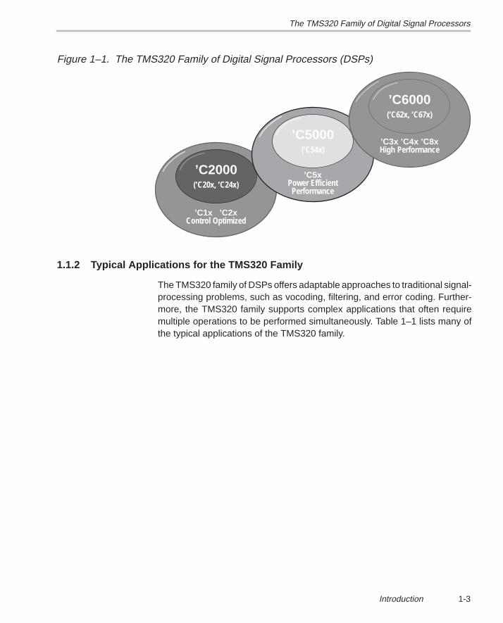
Each generation of TMS320 devices uses a core central processing unit (CPU)that is combined with a variety of on-chip memory and peripheral configurations.These various configurations satisfy a wide range of needs in the worldwide elec-tronics market. When memory and peripherals are integrated with a CPU into onechip, the overall system cost is greatly reduced, and circuit board space isreduced. Figure 1–1 shows the progression of the TMS320 family of devices.
The TMS320 Family of Digital Signal Processors
1-3Introduction
Figure 1–1. The TMS320 Family of Digital Signal Processors (DSPs)
’C2000(’C20x, ’C24x)
’C1x ’C2xControl Optimized
’C5000(’C54x)
’C5xPower EfficientPerformance
’C6000(’C62x, ’C67x)
’C3x ’C4x ’C8xHigh Performance
1.1.2 Typical Applications for the TMS320 Family
The TMS320 family of DSPs offers adaptable approaches to traditional signal-processing problems, such as vocoding, filtering, and error coding. Further-more, the TMS320 family supports complex applications that often requiremultiple operations to be performed simultaneously. Table 1–1 lists many ofthe typical applications of the TMS320 family.

The TMS320 Family of Digital Signal Processors
1-4
Table 1–1. Typical Applications for the TMS320 Family of Digital Signal Processors (DSPs)
Automotive Consumer Control
Adaptive ride controlAntiskid brakesCellular telephonesDigital radiosEngine controlGlobal positioningNavigationVibration analysisVoice commands
Digital radios/TVsEducational toysMusic synthesizersPagersPower toolsRadar detectorsSolid-state answering machines
Disk drive controlEngine controlLaser printer controlMotor controlRobotics controlServo control
General-Purpose Graphics/Imaging Industrial
Adaptive filteringConvolutionCorrelationDigital filteringFast Fourier transformsHilbert transformsWaveform generationWindowing
3-D computingAnimation/digital mapsHomomorphic processingImage compression/transmissionImage enhancement Pattern recognitionRobot visionWorkstations
Numeric controlPower-line monitoringRoboticsSecurity access
Instrumentation Medical Military
Digital filteringFunction generationPattern matchingPhase-locked loopsSeismic processingSpectrum analysisTransient analysis
Diagnostic equipmentFetal monitoringHearing aidsPatient monitoringProstheticsUltrasound equipment
Image processingMissile guidanceNavigationRadar processingRadio frequency modemsSecure communicationsSonar processing
Telecommunications Voice/Speech
1200- to 56 600-bps modemsAdaptive equalizersADPCM transcodersBase stationsCellular telephonesChannel multiplexingData encryptionDigital PBXsDigital speech interpolation (DSI)DTMF encoding/decodingEcho cancellation
FaxingFuture terminalsLine repeatersPersonal communications
systems (PCS)Personal digital assistants (PDA)Speaker phonesSpread spectrum communicationsDigital subscriber loop (xDSL)Video conferencingX.25 packet switching
Speaker verificationSpeech enhancementSpeech recognitionSpeech synthesisSpeech vocodingText-to-speechVoice mail

Introduction to the TMS320C6000 Platform of Digital Signal Processors
1-5Introduction
1.2 Introduction to the TMS320C6000 Platform of Digital Signal Processors
With performance of up to 2000 million instructions per second (MIPS) at 250MHz and a complete set of development tools, the TMS320C6000 DSPs offercost-effective solutions to high-performance DSP programming challenges. TheTMS320C6000 development tools include a new C compiler, an assemblyoptimizer that simplifies programming and scheduling, and a Windowsdebugger interface.
The TMS320C6000 DSPs give system architects unlimited possibilities to dif-ferentiate their products. High performance, ease of use, and affordable pric-ing make the TMS320C6000 platform the ideal solution for multichannel, mul-tifunction applications, such as:
� Pooled modems� Wireless local loop base stations� Beam-forming base stations� Remote access servers (RAS)� Digital subscriber loop (DSL) systems� Cable modems� Multichannel telephony systems� Virtual reality 3-D graphics� Speech recognition� Audio� Radar� Atmospheric modeling� Finite element analysis� Imaging (examples: fingerprint recognition, ultrasound, and MRI)
The TMS320C6000 platform is also an ideal solution for exciting new applica-tions; for example:
� Personalized home security with face and hand/fingerprint recognition
� Advanced cruise control with global positioning systems (GPS) navigationand accident avoidance
� Remote medical diagnostics
Features and Options of the TMS320C62x/C67x Devices
1-6
1.3 Features and Options of the TMS320C62x/C67x Devices
The ’C6211, ’C6701, ’C6201, and ’C6202 devices operate at 150, 167, 200,and 250 MHz respectively (6.67-, 6-, 5-, and 4-ns cycle times). All of theseDSPs execute up to eight 32-bit instructions every cycle. The core CPU con-sists of 32 general-purpose registers of 32-bit word length and eight functionalunits:
� Two multipliers� Six ALUs
The ’C62x/C67x devices have a complete set of optimized development tools,including an efficient C compiler, an assembly optimizer for simplified assem-bly-language programming and scheduling, and a Windows-based debuggerinterface for visibility into source code execution characteristics. A hardwareemulation board, compatible with the TI XDS510 emulator interface, is alsoavailable. This tool complies with IEEE Standard 1149.1–1990, IEEE Stan-dard Test Access Port and Boundary-Scan Architecture.
Features of the ’C62x/C67x include:
� Advanced VLIW CPU with eight functional units, including two multipliersand six arithmetic units
� Executes up to eight instructions per cycle for up to ten times theperformance of typical DSPs
� Allows designers to develop highly effective RISC-like code for fastdevelopment time
� Instruction packing
� Gives code size equivalence for eight instructions executed serially orin parallel
� Reduces code size, program fetches, and power consumption
� All instructions execute conditionally.
� Reduces costly branching
� Increases parallelism for higher sustained performance
� Code executes as programmed on independent functional units.
� Industry’s most efficient C compiler on DSP benchmark suite
� Industry’s first assembly optimizer for fast development and improvedparallelization
� 8/16/32-bit data support, providing efficient memory support for a varietyof applications
Features and Options of the TMS320C62x/C67x Devices
1-7Introduction
� 40-bit arithmetic options that add extra precision for vocoders and othercomputationally intensive applications
� Saturation and normalization provide support for key arithmetic opera-tions.
� Field manipulation and instruction extract, set, clear, and bit countingsupport common operation found in control and data manipulationapplications.
The ’C67x has the following features:
� Peak 1336 MIPS at 167 MHz
� Peak 1G FLOPS at 167 MHz for single-precision operations
� Peak 250M FLOPS at 167 MHz for double-precision operations
� Peak 688M FLOPS at 167 MHz for multiply and accumulate operations
� Hardware support for single-precision (32-bit) and double-precision(64-bit) IEEE floating-point operations.
� 32 � 32-bit integer multiply with 32- or 64-bit result.
A variety of memory and peripheral options are available for the ’C62x/C67x:
� Large on-chip RAM for fast algorithm execution
� 32-bit external memory interface supports SDRAM, SBSRAM, SRAM,and other asynchronous memories, for a broad range of external memoryrequirements and maximum system performance
� Host port access to ’C62x/C67x memory and peripherals
� Multichannel DMA controller
� Multichannel serial port(s)
� 32-bit timer(s)
2-1
CPU Architecture
The VelociTI architecture makes the ’C6000 DSPs the first off-the-shelf DSPsto use an enhancement of traditional VLIW to achieve high performancethrough increased instruction-level parallelism. A traditional VLIW architectureconsists of multiple execution units running in parallel that perform multipleinstructions during a single clock cycle. Parallelism is the key to extremely highperformance and takes these next-generation DSPs well beyond the perfor-mance capabilities of traditional superscalar designs. VelociTI is a highlydeterministic architecture, with few restrictions on how or when instructionsare fetched, executed, or stored. This architectural flexibility is key to thebreakthrough efficiency levels of the ’C6000 compiler.
Topic Page
2.1 TMS320C62x/C67x Block Diagram 2-2. . . . . . . . . . . . . . . . . . . . . . . . . . . . . .
2.2 Central Processing Unit (CPU) 2-3. . . . . . . . . . . . . . . . . . . . . . . . . . . . . . . . .
2.3 CPU Data Paths 2-4. . . . . . . . . . . . . . . . . . . . . . . . . . . . . . . . . . . . . . . . . . . . . . .
2.4 Mapping Between Instructions and Functional Units 2-11. . . . . . . . . . . .
2.5 Addressing Modes 2-18. . . . . . . . . . . . . . . . . . . . . . . . . . . . . . . . . . . . . . . . . . .
2.6 Interrupts 2-19. . . . . . . . . . . . . . . . . . . . . . . . . . . . . . . . . . . . . . . . . . . . . . . . . . .
Chapter 2
TMS320C62x/C67x Block Diagram
2-2
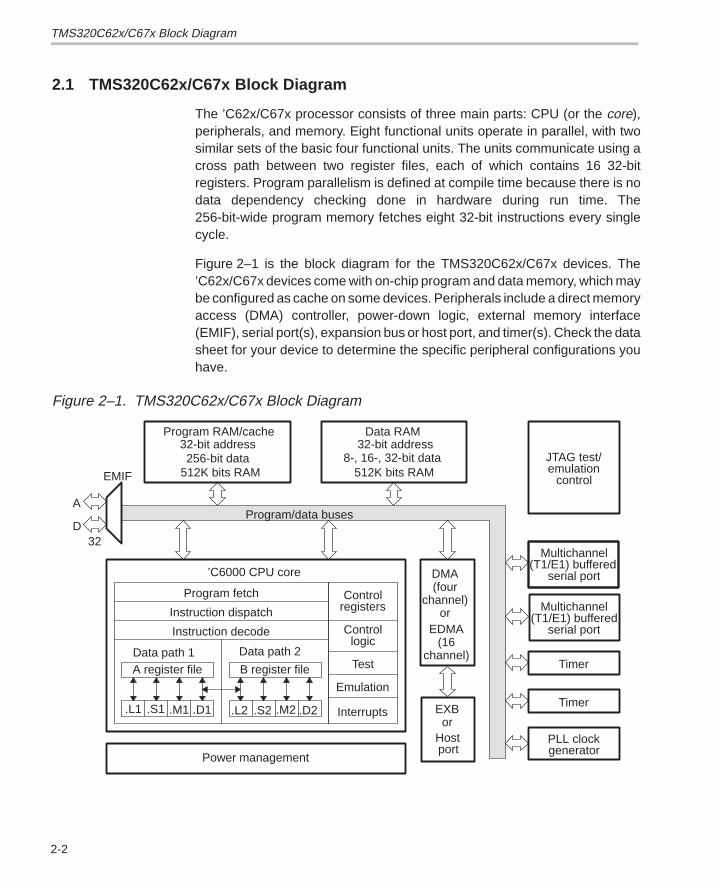
2.1 TMS320C62x/C67x Block Diagram
The ’C62x/C67x processor consists of three main parts: CPU (or the core),peripherals, and memory. Eight functional units operate in parallel, with twosimilar sets of the basic four functional units. The units communicate using across path between two register files, each of which contains 16 32-bitregisters. Program parallelism is defined at compile time because there is nodata dependency checking done in hardware during run time. The256-bit-wide program memory fetches eight 32-bit instructions every singlecycle.
Figure 2–1 is the block diagram for the TMS320C62x/C67x devices. The’C62x/C67x devices come with on-chip program and data memory, which maybe configured as cache on some devices. Peripherals include a direct memoryaccess (DMA) controller, power-down logic, external memory interface(EMIF), serial port(s), expansion bus or host port, and timer(s). Check the datasheet for your device to determine the specific peripheral configurations youhave.
Figure 2–1. TMS320C62x/C67x Block Diagram
Program/data buses
EMIF
32D
A
controlemulationJTAG test/
Data RAM32-bit address
8-, 16-, 32-bit data512K bits RAM512K bits RAM
256-bit data32-bit address
Program RAM/cache
generatorPLL clock
Timer
Timer
serial port(T1/E1) buffered
Multichannel
serial port(T1/E1) buffered
Multichannel
Power managementportHost
DMA(four
channel)or
’C6000 CPU core
Interrupts
Emulation
Test
logicControl
registersControl
Data path 2
.D2.S2 .M2
B register file
.L2.D1.M1.S1.L1
A register fileData path 1
Instruction decode
Instruction dispatch
Program fetch
EDMA(16
channel)
EXBor
Central Processing Unit (CPU)
2-3CPU Architecture
2.2 Central Processing Unit (CPU)
The ’C62x/C67x CPU, in Figure 2–1, is common to all the ’C62x/C67x devices.The CPU contains:
� Program fetch unit� Instruction dispatch unit� Instruction decode unit� 32 32-bit registers� Two data paths, each with four functional units� Control registers� Control logic� Test, emulation, and interrupt logic
The CPU has two data paths (A and B) in which processing occurs. Each datapath has four functional units (.L, .S, .M, and .D) and a register file containing16 32-bit registers. The functional units execute logic, shifting, multiply, anddata address operations. All instructions except loads and stores operate onthe registers. The two data-addressing units (.D1 and .D2) are exclusivelyresponsible for all data transfers between the register files and memory.
The four functional units of a data path have a single data bus connected toregisters on the other side of the CPU so that the units can exchange data withthe register file on the opposite side. Register access across the CPU supportsone read and write operation per cycle.
The two sets of functional units include the following items:
� Two multipliers� Six arithmetic logic units (ALUs)� Two register files, each containing 16 32-bit registers
Each functional unit is controlled by a 32-bit instruction. The instruction fetch,instruction dispatch, and instruction decode blocks can deliver up to eight 32-bitinstructions from the program memory to the functional units every cycle. Thecontrol register file provides methods to configure and control various aspectsof processor operation. Access to the control registers is provided from data-path B.
The VLIW processing flow begins when a 256-bit-wide instruction fetch packet(IFP) is fetched from the internal program memory. The instructions linkedtogether for simultaneous execution (up to eight instructions) form an executepacket. For more details on the processing, see the data sheet for your particu-lar device.
CPU Data Paths
2-4
2.3 CPU Data Paths
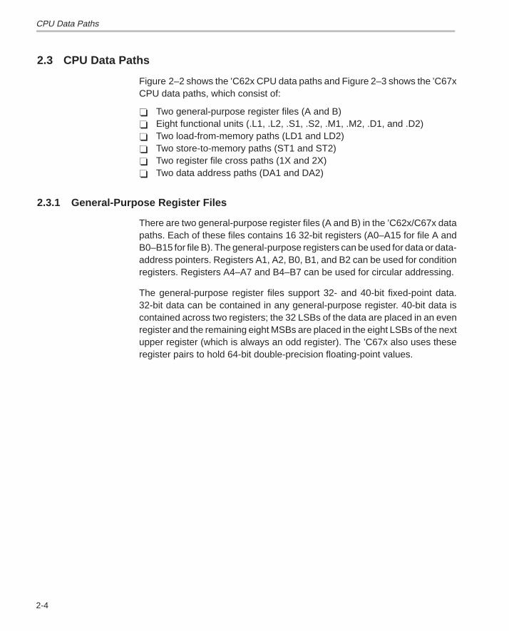
Figure 2–2 shows the ’C62x CPU data paths and Figure 2–3 shows the ’C67xCPU data paths, which consist of:
� Two general-purpose register files (A and B)� Eight functional units (.L1, .L2, .S1, .S2, .M1, .M2, .D1, and .D2)� Two load-from-memory paths (LD1 and LD2)� Two store-to-memory paths (ST1 and ST2)� Two register file cross paths (1X and 2X)� Two data address paths (DA1 and DA2)
2.3.1 General-Purpose Register Files
There are two general-purpose register files (A and B) in the ’C62x/C67x datapaths. Each of these files contains 16 32-bit registers (A0–A15 for file A andB0–B15 for file B). The general-purpose registers can be used for data or data-address pointers. Registers A1, A2, B0, B1, and B2 can be used for conditionregisters. Registers A4–A7 and B4–B7 can be used for circular addressing.
The general-purpose register files support 32- and 40-bit fixed-point data.32-bit data can be contained in any general-purpose register. 40-bit data iscontained across two registers; the 32 LSBs of the data are placed in an evenregister and the remaining eight MSBs are placed in the eight LSBs of the nextupper register (which is always an odd register). The ’C67x also uses theseregister pairs to hold 64-bit double-precision floating-point values.

CPU Data Paths
2-5CPU Architecture
Figure 2–2. TMS320C62x CPU Data Paths
ÁÁÁÁÁÁÁÁÁÁÁÁÁÁÁÁÁÁÁÁÁÁÁÁÁÁÁÁÁÁÁÁÁÁÁÁÁÁÁÁÁÁÁÁÁÁÁÁÁÁÁÁÁÁÁÁÁÁÁÁÁÁÁÁ
ÁÁÁÁÁÁÁÁÁÁÁÁÁÁÁÁÁÁÁÁÁÁÁÁÁÁÁÁÁÁÁÁÁÁÁÁÁÁÁÁÁÁÁÁÁÁÁÁÁÁÁÁÁÁÁÁÁÁÁÁÁÁÁÁÁÁÁÁ
ÁÁÁÁÁÁÁÁÁÁÁÁÁÁÁÁÁÁÁÁÁÁÁÁ
ÁÁÁÁÁÁÁÁÁÁÁÁÁÁÁÁÁÁÁÁÁÁÁÁ
ÁÁÁÁÁÁÁÁÁÁÁÁÁÁÁÁÁÁÁÁ
ÁÁÁÁÁÁÁÁÁÁÁÁ
ÁÁÁÁÁÁÁÁÁÁÁÁ
ÁÁÁÁÁÁÁÁÁÁÁÁÁÁÁÁ
ÁÁÁÁÁÁÁÁÁÁÁÁÁÁÁÁÁÁÁÁÁÁÁÁ
2X
1X
.L2
.S2
.M2
.D2
(B0–B15)
(A0–A15)
ÁÁÁÁ
ÁÁÁÁ
ÁÁ
ÁÁÁÁÁÁ
ÁÁÁ
ÁÁ
ÁÁ
ÁÁ
Á
ÁÁÁ
Á
Á
Á
ÁÁÁ
ÁÁÁ
ÁÁ
ÁÁÁ
Á .D1
.M1
ÁÁÁ
ÁÁÁÁÁÁ
ÁÁÁÁÁÁÁ
Á
.S1
ÁÁÁÁÁ
ÁÁ
.L1
long src
dst
src2
src1
ÁÁÁ
ÁÁÁÁÁ
ÁÁÁÁ
src1
src1
src1
src1
src1
src1
src1
8
8
8
8
88
long dst
long dstdst
dst
dst
dst
dst
dst
dst
src2
src2
src2
src2
src2
src2
src2
long src
Controlregister
fileÁÁ
DA1
DA2
ST1
LD1
LD2
ST2
32
32
Data path A
Data path B
Register file A
Register file B
long srclong dst
long dstlong src

CPU Data Paths
2-6
Figure 2–3. TMS320C67x CPU and Data Paths
8
8
ÁÁÁÁÁÁÁÁÁÁÁÁÁÁÁÁÁÁÁÁÁÁÁÁÁÁÁÁÁÁÁÁÁÁÁÁÁÁÁÁÁÁÁÁÁÁÁÁÁÁÁÁÁÁÁÁÁÁÁÁÁÁÁÁÁÁÁÁÁÁÁÁÁÁÁÁÁÁÁÁÁÁÁÁÁ
ÁÁÁÁÁÁÁÁÁÁÁÁÁÁÁÁÁÁÁÁÁÁÁÁÁÁÁÁÁÁÁÁÁÁÁÁÁÁÁÁÁÁÁÁÁÁÁÁÁÁÁÁÁÁÁÁÁÁÁÁÁÁÁÁÁÁÁÁÁÁÁÁÁÁÁÁÁÁÁÁÁÁÁÁÁ
ÁÁÁÁÁÁÁÁÁÁÁÁÁÁÁÁÁÁÁÁÁÁÁÁ
ÁÁÁÁÁÁÁÁÁÁÁÁÁÁÁÁÁÁÁÁÁÁÁÁ
ÁÁÁÁÁÁÁÁÁÁÁÁÁÁÁÁ
ÁÁÁÁÁÁÁÁÁÁÁÁ
ÁÁÁÁÁÁÁÁÁÁÁÁ
ÁÁÁÁÁÁÁÁÁÁÁÁÁÁÁÁÁÁÁÁ
ÁÁÁÁÁÁÁÁÁÁÁÁÁÁÁÁÁÁÁÁÁÁÁÁ
2X
1X
.L2
.S2
.M2
.D2
(B0–B15)
(A0–A15)
ÁÁ
Á
ÁÁ
Á
ÁÁÁÁ
ÁÁÁÁ
ÁÁÁÁ
ÁÁ
ÁÁ
ÁÁ
ÁÁ
ÁÁ
ÁÁ
ÁÁÁÁ
ÁÁÁ
ÁÁÁ
ÁÁ.D1
.M1
ÁÁÁÁÁÁ
ÁÁ
ÁÁÁÁÁ
ÁÁÁÁ
.S1
ÁÁÁÁÁÁ
ÁÁÁÁ
Á
.L1
long src
dst
src2
src1
ÁÁÁÁ
ÁÁ
ÁÁÁÁ
ÁÁÁÁ
src1
src1
src1
src1
src1
src1
src1
8
8
long dst
long dstdst
dst
dst
dst
dst
dst
dst
src2
src2
src2
src2
src2
src2
src2
long src
Controlregister
fileÁ
DA1
DA2
ST1
LD1 32 LSB
LD2 32 LSB
LD2 32 MSB
32
32
Data path A
Data path B
Register file A
Register file B
long srclong dst
long dstlong src
ÁÁLD1 32 MSB
32
ST2
32
8
8
8
8
ÁÁ
Á
CPU Data Paths
2-7CPU Architecture
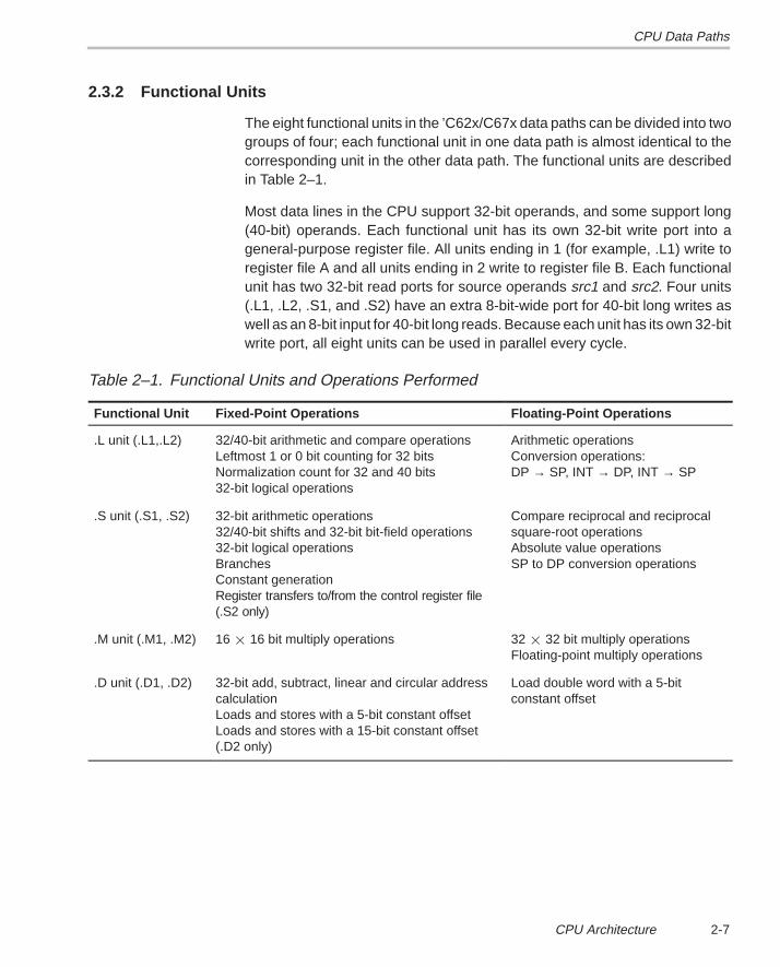
2.3.2 Functional Units
The eight functional units in the ’C62x/C67x data paths can be divided into twogroups of four; each functional unit in one data path is almost identical to thecorresponding unit in the other data path. The functional units are describedin Table 2–1.
Most data lines in the CPU support 32-bit operands, and some support long(40-bit) operands. Each functional unit has its own 32-bit write port into ageneral-purpose register file. All units ending in 1 (for example, .L1) write toregister file A and all units ending in 2 write to register file B. Each functionalunit has two 32-bit read ports for source operands src1 and src2. Four units(.L1, .L2, .S1, and .S2) have an extra 8-bit-wide port for 40-bit long writes aswell as an 8-bit input for 40-bit long reads. Because each unit has its own 32-bitwrite port, all eight units can be used in parallel every cycle.
Table 2–1. Functional Units and Operations Performed
Functional Unit Fixed-Point Operations Floating-Point Operations
.L unit (.L1,.L2) 32/40-bit arithmetic and compare operationsLeftmost 1 or 0 bit counting for 32 bitsNormalization count for 32 and 40 bits32-bit logical operations
Arithmetic operationsConversion operations:DP → SP, INT → DP, INT → SP
.S unit (.S1, .S2) 32-bit arithmetic operations32/40-bit shifts and 32-bit bit-field operations32-bit logical operationsBranchesConstant generationRegister transfers to/from the control register file (.S2 only)
Compare reciprocal and reciprocalsquare-root operationsAbsolute value operationsSP to DP conversion operations
.M unit (.M1, .M2) 16 � 16 bit multiply operations 32 � 32 bit multiply operationsFloating-point multiply operations
.D unit (.D1, .D2) 32-bit add, subtract, linear and circular addresscalculationLoads and stores with a 5-bit constant offsetLoads and stores with a 15-bit constant offset (.D2 only)
Load double word with a 5-bitconstant offset

CPU Data Paths
2-8
2.3.3 TMS320C62x/C67x Control Register Files
One unit (.S2) can read from and write to the control register file, shown inFigure 2–2 and Figure 2–3. Table 2–2 lists the control registers contained inthe control register file and describes each. Each control register is accessedby the MVC instruction.
Table 2–2. Control Registers
Register
Abbreviation Name Description
AMR Addressing mode register Specifies whether to use linear or circular addressing foreach of eight registers; also contains sizes for circular ad-dressing
CSR Control status register Contains the global interrupt enable bit, cache control bits,and other miscellaneous control and status bits
IFR Interrupt flag register Displays status of interrupts
ISR Interrupt set register Allows you to set pending interrupts manually
ICR Interrupt clear register Allows you to clear pending interrupts manually
IER Interrupt enable register Allows enabling/disabling of individual interrupts
ISTP Interrupt service table pointer Points to the beginning of the interrupt service table
IRP Interrupt return pointer Contains the address to be used to return from a maskableinterrupt
NRP Nonmaskable interrupt returnpointer
Contains the address to be used to return from a nonmask-able interrupt
PCE1 Program counter, E1 phase Contains the address of the fetch packet that contains theexecute packet in the E1 pipeline stage

CPU Data Paths
2-9CPU Architecture
2.3.4 TMS320C67x Control Register File Extensions
The ’C67x has three additional configuration registers to support floating pointoperations (see Table 2–3). The registers specify the desired floating-pointrounding mode for the .L and .M units. They also contain bit fields to warn ifsrc1 and src2 are NaN (not a number) or denormal numbers, and if the resultoverflows, underflows, is inexact, infinite, or invalid. There are also fields towarn if a divide by 0 was performed, or if a compare was attempted with a NaNsource.
Table 2–3. TMS320C67x Control Register File Extensions
Register
Abbreviation Name Description
FADCR Floating-point adder configura-tion register
Specifies underflow mode, rounding mode, NaNs, and otherexceptions for the .L unit.
FAUCR Floating-point auxiliary configu-ration register
Specifies underflow mode, rounding mode, NaNs, and otherexceptions for the .S unit.
FMCR Floating-point multiplier configu-ration register
Specifies underflow mode, rounding mode, NaNs, and otherexceptions for the .M unit.
2.3.5 Register File Cross Paths
Each functional unit reads directly from and writes directly to the register filewithin its own data path. That is, the .L1, .S1, .D1, and .M1 units write to registerfile A and the .L2, .S2, .D2, and .M2 units write to register file B. The registerfiles are connected to the opposite-side register file’s functional units via the1X and 2X cross paths. These cross paths allow functional units from one datapath to access a 32-bit operand from the opposite side’s register file. The 1Xcross path allows data path A’s functional units to read their source from regis-ter file B and the 2X cross path allows data path B’s functional units to read theirsource from register file A.
Six of the functional units have access to the opposite side’s register file viaa cross path. The .M1, .M2, .S1, and .S2 units’ src2 inputs are multiplex-select-able between the cross path and the same side register file. The .L1 and .L2units’ src1 and src2 inputs are also multiplex-selectable between the crosspath and the same side register file.
Only two cross paths, 1X and 2X, exist in the ’C62x/C67x CPUs. This limits onesource read from each data path’s opposite register file per cycle, or two cross-path source reads per cycle.
CPU Data Paths
2-10
2.3.6 Memory, Load, and Store Paths
There are two 32-bit paths for loading data from memory to the register file:LD1 for register file A, and LD2 for register file B. The ’C67x also has a second32-bit load path for both register files A and B, which allows the LDDWinstruction to simultaneously load two 32-bit registers into side A and two32-bit registers into side B. There are also two 32-bit paths, ST1 and ST2, forstoring register values to memory from each register file. The store paths areshared with the .L and .S long read paths.
2.3.7 Data-Address Paths
The data-address paths (DA1 and DA2) shown in Figure 2–2 and Figure 2–3coming out of the .D units allow data addresses generated from one registerfile to support loads and stores to memory from the other register file. However,loads and stores executed in parallel must load to and from the same registerfile or both use a crosspath to the opposite register.

Mapping Between Instructions and Functional Units
2-11CPU Architecture
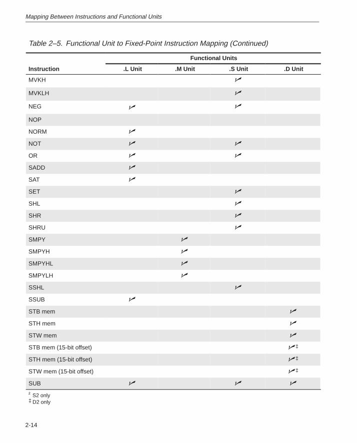
2.4 Mapping Between Instructions and Functional Units
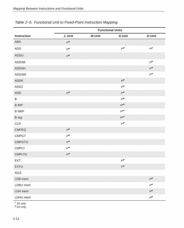
Table 2–4 shows the mapping between instructions and functional units andTable 2–5 shows the mapping between functional units and instructions for theTMS320C62x/C67x fixed-point instructions.
Table 2–4. Fixed-Point Instruction to Functional Unit Mapping
.L Unit .M Unit .S Unit .D Unit
ABS MPY ADD SET ADD STB (15-bit offset)‡
ADD MPYU ADDK SHL ADDAB STH (15-bit offset)‡
ADDU MPYUS ADD2 SHR ADDAH STW (15-bit offset)‡
AND MPYSU AND SHRU ADDAW SUB
CMPEQ MPYH B disp SHRL LDB SUBAB
CMPGT MPYHU B IRP† SUB LDBU SUBAH
CMPGTU MPYHUS B NRP† SUBU LDH SUBAW
CMPLT MPYHSU B reg SUB2 LDHU ZERO
CMPLTU MPYHL CLR XOR LDW
LMBD MPYHLU EXT ZERO LDB (15-bit offset)‡
MV MPYHULS EXTU LDBU (15-bit offset)‡
NEG MPYHSLU MV LDH (15-bit offset)‡
NORM MPYLH MVC† LDHU (15-bit offset)‡
NOT MPYLHU MVK LDW (15-bit offset)‡
OR MPYLUHS MVKH MV
SADD MPYLSHU MVKLH STB
SAT SMPY NEG STH
SSUB SMPYHL NOT STW
SUB SMPYLH OR
SUBU SMPYH
SUBC
XOR
ZERO
† S2 only‡ D2 only
Mapping Between Instructions and Functional Units
2-12
Table 2–5. Functional Unit to Fixed-Point Instruction Mapping
Functional Units
Instruction .L Unit .M Unit .S Unit .D Unit
ABS �
ADD � � �
ADDU �
ADDAB �
ADDAH �
ADDAW �
ADDK �
ADD2 �
AND � �
B �
B IRP �†
B NRP �†
B reg �†
CLR �
CMPEQ �
CMPGT �
CMPGTU �
CMPLT �
CMPLTU �
EXT �
EXTU �
IDLE
LDB mem �
LDBU mem �
LDH mem �
LDHU mem �
† S2 only‡ D2 only

Mapping Between Instructions and Functional Units
2-13CPU Architecture
Table 2–5. Functional Unit to Fixed-Point Instruction Mapping (Continued)
Functional Units
Instruction .D Unit.S Unit.M Unit.L Unit
LDW mem �
LDB mem (15-bit offset) �‡
LDBU mem (15-bit offset) �‡
LDH mem (15-bit offset) �‡
LDHU mem (15-bit offset) �‡
LDW mem (15-bit offset) �‡
LMBD �
MPY �
MPYU �
MPYUS �
MPYSU �
MPYH �
MPYHU �
MPYHUS �
MPYHSU �
MPYHL �
MPYHLU �
MPYHULS �
MPYHSLU �
MPYLH �
MPYLHU �
MPYLUHS �
MPYLSHU �
MV � � �
MVC† �
MVK �
† S2 only‡ D2 only
Mapping Between Instructions and Functional Units
2-14
Table 2–5. Functional Unit to Fixed-Point Instruction Mapping (Continued)
Functional Units
Instruction .D Unit.S Unit.M Unit.L Unit
MVKH �
MVKLH �
NEG � �
NOP
NORM �
NOT � �
OR � �
SADD �
SAT �
SET �
SHL �
SHR �
SHRU �
SMPY �
SMPYH �
SMPYHL �
SMPYLH �
SSHL �
SSUB �
STB mem �
STH mem �
STW mem �
STB mem (15-bit offset) �‡
STH mem (15-bit offset) �‡
STW mem (15-bit offset) �‡
SUB � � �
† S2 only‡ D2 only

Mapping Between Instructions and Functional Units
2-15CPU Architecture
Table 2–5. Functional Unit to Fixed-Point Instruction Mapping (Continued)
Functional Units
Instruction .D Unit.S Unit.M Unit.L Unit
SUBU � �
SUBAB �
SUBAH �
SUBAW �
SUBC �
SUB2 �
XOR � �
ZERO � � �
† S2 only‡ D2 only
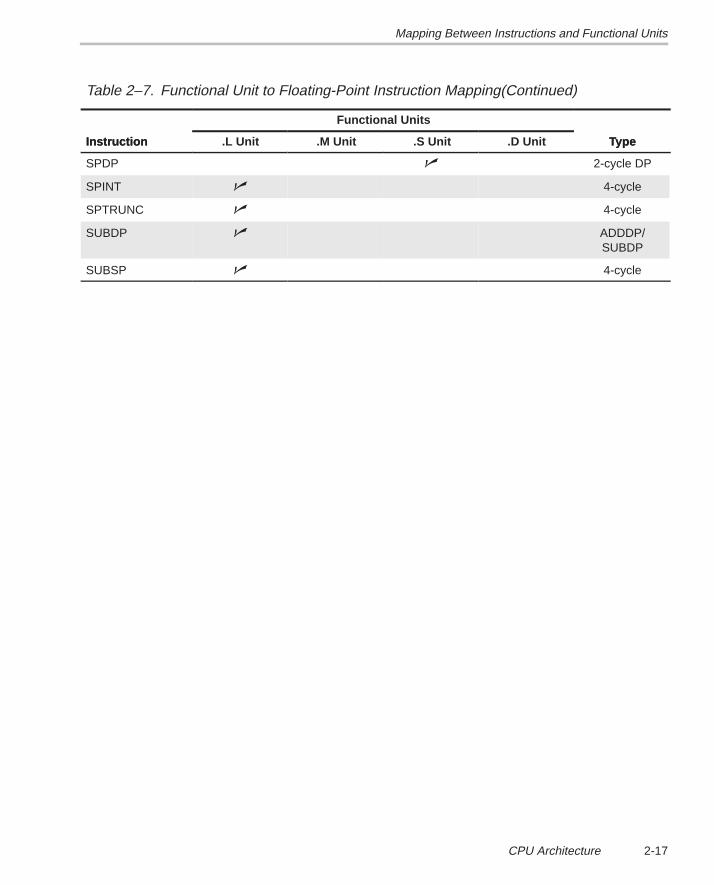
Table 2–6 shows the mapping between instructions and functional units andTable 2–7 shows the mapping between functional units and instructions for theTMS320C67x floating-point instructions.
Table 2–6. Floating-Point Instruction to Functional Unit Mapping
.L Unit .M Unit .S Unit .D Unit
ADDDP MPYDP ABSDP ADDAD
ADDSP MPYI ABSSP LDDW
DPINT MPYID CMPEQDP
DPSP MPYSP CMPEQSP
INTDP CMPGTDP
INTDPU CMPGTSP
INTSP CMPLTDP
INTSPU CMPLTSP
SPINT RCPDP
SPTRUNC RCPSP
SUBDP RSQRDP
SUBSP RSQRSP
SPDP

Mapping Between Instructions and Functional Units
2-16
Table 2–7. Functional Unit to Floating-Point Instruction Mapping
Functional Units
Instruction .L Unit .M Unit .S Unit .D Unit Type
ABSDP � 2-cycle DP
ABSSP � Single cycle
ADDAD � Single cycle
ADDDP � ADDDP/SUBDP
ADDSP � Four cycle
CMPEQDP � DP compare
CMPEQSP � Single cycle
CMPGTDP � DP compare
CMPGTSP � Single cycle
CMPLTDP � DP compare
CMPLTSP � Single cycle
DPINT � 4-cycle
DPSP � 4-cycle
DPTRUNC � 4-cycle
INTDP � INTDP
INTDPU � INTDP
INTSP � 4-cycle
INTSPU � 4-cycle
LDDW � Load
MPYDP � MPYDP
MPYI � MPYI
MPYID � MPYID
MPYSP � 4-cycle
RCPDP � 2-cycle DP
RCPSP � Single cycle
RSQRDP � 2-cycle DP
RSQRSP � Single cycle
Mapping Between Instructions and Functional Units
2-17CPU Architecture
Table 2–7. Functional Unit to Floating-Point Instruction Mapping(Continued)
Instruction Type
Functional Units
Instruction Type.D Unit.S Unit.M Unit.L Unit
SPDP � 2-cycle DP
SPINT � 4-cycle
SPTRUNC � 4-cycle
SUBDP � ADDDP/SUBDP
SUBSP � 4-cycle
Addressing Modes
2-18
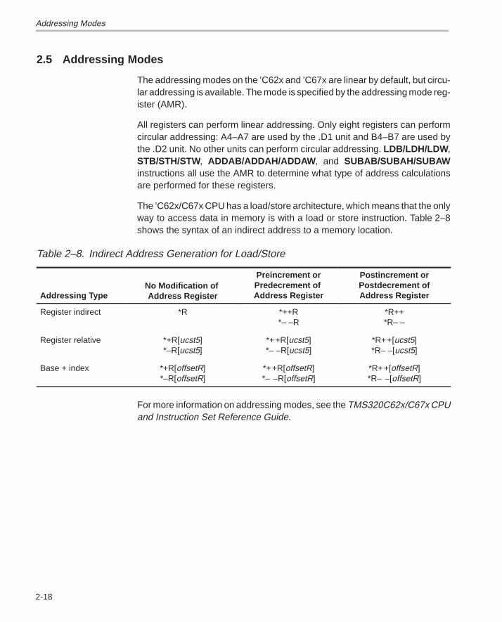
2.5 Addressing Modes
The addressing modes on the ’C62x and ’C67x are linear by default, but circu-lar addressing is available. The mode is specified by the addressing mode reg-ister (AMR).
All registers can perform linear addressing. Only eight registers can performcircular addressing: A4–A7 are used by the .D1 unit and B4–B7 are used bythe .D2 unit. No other units can perform circular addressing. LDB/LDH/LDW ,STB/STH/STW, ADDAB/ADDAH/ADDAW , and SUBAB/SUBAH/SUBAWinstructions all use the AMR to determine what type of address calculationsare performed for these registers.
The ’C62x/C67x CPU has a load/store architecture, which means that the onlyway to access data in memory is with a load or store instruction. Table 2–8shows the syntax of an indirect address to a memory location.
Table 2–8. Indirect Address Generation for Load/Store
Addressing TypeNo Modification of Address Register
Preincrement orPredecrement of Address Register
Postincrement orPostdecrement ofAddress Register
Register indirect *R *++R*– –R
*R++*R– –
Register relative *+R[ucst5]*–R[ucst5]
*++R[ucst5]*– –R[ucst5]
*R++[ucst5]*R– –[ucst5]
Base + index *+R[offsetR]*–R[offsetR]
*++R[offsetR]*– –R[offsetR]
*R++[offsetR]*R– –[offsetR]
For more information on addressing modes, see the TMS320C62x/C67x CPUand Instruction Set Reference Guide.

Interrupts
2-19CPU Architecture
2.6 Interrupts
The ’C62x/C67x CPU has 14 interrupts. These are reset, the nonmaskableinterrupt (NMI), and interrupts 4–15. These interrupts correspond to theRESET, NMI, and INT4–INT15 signals on the CPU boundary. In some’C62x/C67x devices, these signals may be tied directly to pins on the device,connected to on-chip peripherals, or may be disabled permanently by beingtied inactive on chip. Generally, RESET and NMI are connected directly to pinson the device. Characteristics of interrupt servicing include:
� The IACK pin from the CPU is used to acknowledge an interrupt request.
� The INUM0–INUM3 pins indicate which interrupt vector is being serviced.
� Interrupt vectors are relocatable.
� Interrupt vectors consist of one fetch packet which provides for quickservicing.
For more information on interrupts, see the TMS320C62x/C67x CPU andInstruction Set Reference Guide, the TMS320C6201/C6701 Peripherals Ref-erence Guide, and the TMS320C6202/C6211 Peripherals Reference GuideAddendum.

3-1
Memory
The TMS320C6000 platform of devices includes on-chip memory for both pro-gram and data, some of which may be selected as cache. In addition, an exter-nal memory interface (EMIF) may be used to include external memories in a’C6000 system.
Topic Page
3.1 Memory Maps 3-2. . . . . . . . . . . . . . . . . . . . . . . . . . . . . . . . . . . . . . . . . . . . . . . . .
3.2 Internal Memory 3-4. . . . . . . . . . . . . . . . . . . . . . . . . . . . . . . . . . . . . . . . . . . . . .
3.3 External Memory Interface (EMIF) 3-11. . . . . . . . . . . . . . . . . . . . . . . . . . . . .
Chapter 3

Memory Maps
3-2
3.1 Memory Maps
The memory maps of the ’C6000 platform of devices are shown in Figure 3–1and Figure 3–2. The total memory address range of the ’C6000 devices is4Gbytes (corresponding to 32-bit internal address representation). Eachmemory map is divided into the internal program memory, internal datamemory, external memory spaces, and internal peripheral space.
Figure 3–1. TMS320C6201/C6202/C6701 Memory MapsStarting address Memory map 0
(Direct execution)Block size
(bytes)Starting address Memory map 1
(Boot mode)Block size
(bytes)
0000 0000h External memory spaceCE0
16M 0000 0000h Internal program RAM 64K/(256Kon ’C6202)
0100 0000h External memory spaceCE1
4M 0001 0000h(0004 0000hon ’C6202)
Reserved4M–64K
(4M–256Kon ’C6202)
0140 0000h Internal program RAM 64K/(256Kon ’C6202)
0040 0000h External memory spaceCE0
16M
0141 0000h(0144 0000hon ’C6202)
Reserved4M–64K
(4M–256Kon ’C6202)
0140 0000h External memory spaceCE1
4M
0180 0000h Internal peripherals 8M 0180 0000h Internal peripherals 8M
0200 0000h External memory spaceCE2
16M 0200 0000h External memory spaceCE2
16M
0300 0000h External memory spaceCE3
16M 0300 0000h External memory spaceCE3
16M
0400 0000h Reserved 1G–64M 0400 0000h Reserved 1G–64M
4000 0000h Expansion bus(on ’C6202)
1G 4000 0000h Expansion bus(on ’C6202)
1G
8000 0000h Internal Data RAM 64K/(128Kon ’C6202)
8000 0000h Internal data RAM 64K/(128Kon ’C6202)
8001 0000h8002 0000h Reserved
2G–64K(2G–128Kon ’C6202)
8001 0000h8002 0000h Reserved
2G–64K(2G–128Kon ’C6202)

Memory Maps
3-3Memory
Figure 3–2. TMS320C6211 Memory Map
Starting Address Memory Block Block Size(Bytes)
0000 0000h Internal RAM (L2) 64K
0001 0000h Reserved 24M–64K
0180 0000h Configuration and peripherals 8M
0200 0000h Reserved 224M
1000 0000h External memory 512M
3000 0000h Reserved 256M
4000 0000h McBSP 0/1 Data 256M
5000 0000h Reserved 256M
6000 0000h HPI expansion bus 256M
7000 0000h Reserved 2G + 256M
For the ’C6201 and ’C6701, five BOOTMODE pins determine which memorymap and boot process are used.The ’C6202 has these five pins removed, andinstead latches the expansion bus data lines XD[4:0] on the rising edge ofRESET. These pins should be pulled high or low through resistors to select theboot process and memory map. The ’C6211 has only one memory map, butselects the boot process in similar fashion to the ’C6202. HD[4:3] are sampledfrom the host-port interface on the rising edge of RESET to determine whichboot process will be used.
The two modes of operation for these devices are direct execution and bootmode. In direct execution, the program starts loading from external address0, whereas in boot mode, the program is loaded either from external memoryor from an external host before starting execution at internal address 0.
Internal Memory
3-4
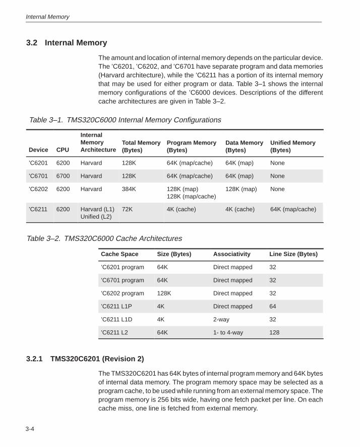
3.2 Internal Memory
The amount and location of internal memory depends on the particular device.The ’C6201, ’C6202, and ’C6701 have separate program and data memories(Harvard architecture), while the ’C6211 has a portion of its internal memorythat may be used for either program or data. Table 3–1 shows the internalmemory configurations of the ’C6000 devices. Descriptions of the differentcache architectures are given in Table 3–2.
Table 3–1. TMS320C6000 Internal Memory Configurations
Device CPU
InternalMemoryArchitecture
Total Memory(Bytes)
Program Memory(Bytes)
Data Memory(Bytes)
Unified Memory(Bytes)
’C6201 6200 Harvard 128K 64K (map/cache) 64K (map) None
’C6701 6700 Harvard 128K 64K (map/cache) 64K (map) None
’C6202 6200 Harvard 384K 128K (map)128K (map/cache)
128K (map) None
’C6211 6200 Harvard (L1)Unified (L2)
72K 4K (cache) 4K (cache) 64K (map/cache)
Table 3–2. TMS320C6000 Cache Architectures
Cache Space Size (Bytes) Associativity Line Size (Bytes)
’C6201 program 64K Direct mapped 32
’C6701 program 64K Direct mapped 32
’C6202 program 128K Direct mapped 32
’C6211 L1P 4K Direct mapped 64
’C6211 L1D 4K 2-way 32
’C6211 L2 64K 1- to 4-way 128
3.2.1 TMS320C6201 (Revision 2)
The TMS320C6201 has 64K bytes of internal program memory and 64K bytesof internal data memory. The program memory space may be selected as aprogram cache, to be used while running from an external memory space. Theprogram memory is 256 bits wide, having one fetch packet per line. On eachcache miss, one line is fetched from external memory.
Internal Memory
3-5Memory
The internal data memory is made up of four 16-bit wide banks. The DMA orCPU may access each bank once per cycle, and multiple banks may be ac-cessed in the same cycle. Since the CPU has two sides (A and B), the datamemory may be accessed by the CPU and DMA up to three times each cycle.
3.2.2 TMS320C6201B (Revision 3)
The TMS320C6201B has 64K bytes of internal program memory and 64K by-tes of internal data memory, like the ’C6201. The program memory space isidentical, and may be selected as a program cache. The program memory is256 bytes wide, having one fetch packet per line. On each cache miss, one lineis fetched from external memory.
The internal data memory is slightly different, modified to maximize the dataaccesses that may be performed each cycle by the three possible sources.Instead of four banks, the ’C6201B is made up of eight 16-bit wide banks.These are divided into two blocks of four banks, with the first four in the lowerhalf of data memory, and the last four in the upper half. The DMA or CPU mayaccess each bank once per cycle, and multiple banks may be accessed in thesame cycle. With this memory configuration, the maximum data access eachcycle is three 32-bit accesses; two CPU accesses and one DMA access.
3.2.3 TMS320C6701
The TMS320C6701 memory configuration is almost identical to that of the’C6201B. It also has 64K bytes of internal program memory and 64K bytes ofinternal data memory, and the program may be selected as a program cache.The program memory line size is 32 bytes, having one fetch packet per line.On each cache miss, one line is fetched from external memory.
The internal data memory consists of two blocks of eight 16-bit banks, ratherthan four 16-bit banks. This feature allows parallel double-precision loads bythe CPU in the same cycle as a data access by the DMA. With the new memoryconfiguration, the maximum data access each cycle is two 64-bit CPU ac-cesses (LDDW only) and 32-bit DMA access.

Internal Memory
3-6
3.2.4 TMS320C6202
The TMS320C6202 has 256K bytes of internal program memory and 128K by-tes of internal data memory. The program memory space consists of two 128K-byte banks, with one bank selectable as a program cache. This can effectivelyprovide 128K bytes of program memory and 128K bytes of program cache, ifselected. The program memory line size is 32 bytes, having one fetch packetper line. On each cache miss, one line is fetched from external memory.
The internal data memory is configured identically to the ’C6201B, with eight16-bit wide banks. These are divided into two blocks of four banks, with the firstfour in the lower half of data memory, and the last four in the upper half. TheDMA or CPU may access each bank once per cycle, and multiple banks maybe accessed in the same cycle. With this memory configuration, the maximumdata access is three 32-bit accesses.
3.2.5 TMS320C6211
The TMS320C6211 has a 4K-byte level-one program cache (L1P) and 4K-byte level-one data cache (L1D). These cache memories are always activeand are not included in the memory map. The L1P line size is 64 bytes (twofetch packets), while the L1D line size is 32 bytes (eight data words). On a missto either cache space, the entire line of the miss is fetched. For the instructioncache, this provides one pre-fetched instruction packet, while the data fetchwill receive adjacent data elements. The level-one caches are transparent tothe user.
The internal memory at address 0 is a unified 64K-byte data and instructionRAM. This memory may be configured in one of five modes to provide a level-two cache (both instruction and data), as shown in Table 3–3. The L2 SRAMspace always begins at address zero, regardless of the cache mode selected.The length will vary.
Internal Memory
3-7Memory
Table 3–3. L2 Operation Modes
L2 Mode Cache Size SRAM size
000 0K 64K
001 16K 1-way 48K
010 32K 2-way 32K
011 48K 3-way 16K
100 Reserved
101 Reserved
110 Reserved
111 64K 4-way 0K
The L2 memory is made up of four 64-bit-wide banks. On an L2 miss, 128 bytesof new data will be requested of the EDMA. The data is always aligned on a32-word boundary.
3.2.6 Data Memory Access
For the ’C6201, ’C6202, and ’C6701 the data memory controller services allrequests to internal data memory by either the CPU or DMA. The ’C6211 hasa level-one data cache (L1D) controller and a level-two cache (L2) controller.The L1D controller services the requests by the CPU and sends them to theL2 controller on a read or a write miss. Data requests by the EDMA go directlyto the L2 controller.
Internal Memory
3-8
3.2.7 TMS320C6201, ’C6202, ’C6701
The CPU sends requests to the data memory controller through the two ad-dress buses (DA1 and DA2). The data to be stored is transmitted through theCPU data store buses (ST1 and ST2). Load data is received through the CPUdata load buses (LD1 and LD2). The CPU data requests are mapped basedon the requested data’s memory address range to the internal data memory,internal peripheral space (through the peripheral bus controller), or the exter-nal memory interface. The data memory controller also connects to the inter-nal data memory and performs CPU/DMA arbitration for the on-chip dataRAM. Figure 3–3 shows the CPU, data memory controller, and peripheral busconnections.
Figure 3–3. TMS320C6201/C6202/C6701 Data Memory Controller Interconnect
Data memory controller
Data
Memory
CPU
EMIF DMA PBUS
Bank 1
Bank 3
Bank 2
...
...
Bank n
DA1 address
ST1 store data
LD1 load data
DA2 address
ST2 store data
LD2 load data
Solid line indicates data
Dashed line indicates request
Arrowheads indicate direction of data or request
Internal Memory
3-9Memory
3.2.8 TMS320C6211
In the TMS320C6211, the CPU sends requests to the L1D controller in thesame fashion as the ’C6201, ’C6202, and ’C6701 request data from the datamemory controller. On a read data miss or a data write, the L1D controllersends a request to the L2 controller to complete the action. The L2 controllermay then access the L2 cache/memory space, or send the request to theEDMA.
Figure 3–4. TMS320C6211 Data Memory Controller Interconnect
L1 datacache
CPU
EDMA
DA1 address
ST1 store data
LD1 load data
DA2 address
ST2 store data
LD2 load data
Solid line indicates data
Dashed line indicates request
Arrowheads indicate direction of data or request
L1Dcache
controller
L2 cachecontroller
L2 datacache/memory

Internal Memory
3-10
3.2.9 Peripheral Bus
The peripherals are configured via a set of memory-mapped control registers.The peripheral bus controller arbitrates all accesses to the control registers.On the ’C6201, ’C6202, and ’C6701, the DMA accesses the peripheral buscontroller directly, while the CPU accesses it through the data memorycontroller.
On the ’C6211, the peripheral bus controller is incorporated into the L2 control-ler. The EDMA accesses this directly, while the CPU accesses it through theL1D controller.
The peripheral bus controller converts all peripheral bus accesses to word ac-cesses. This affects all writes to a control register, as a byte or halfword will betreated as an unsigned 32-bit word. On reads, individual bytes may be ac-cessed.
3.2.10 Expansion Bus
The expansion bus on the ’C6202 is a 32-bit-wide bus that supports a gluelesssynchronous FIFO interface, asynchronous interface, and two host modes.The two host modes are synchronous master/slave mode or asynchronoushost mode. Mode selection is performed during boot using pull-up/down resis-tors. The expansion bus replaces the HPI and expands the memory optionsavailable to the user.
External Memory Interface (EMIF)
3-11Memory
3.3 External Memory Interface (EMIF)
The external memory interface (EMIF) connects the CPU and externalmemory, such as synchronous dynamic RAM (SDRAM), synchronous burststatic RAM (SBSRAM), and asynchronous memory. The EMIF also provides8-bit-wide and 16-bit-wide memory read capability to support low-cost bootROM memories (flash, EEPROM, EPROM, and PROM). The EMIF supportshigh throughput interfaces to SDRAM, including burst capability.
For more information on the EMIF, see section 4.5 of this book and theTMS320C6000 Peripherals Reference Guide. For more information on the ex-pansion bus, see section 4.4. For more information on internal memory, seethe TMS320C6000 Peripherals Reference Guide.

4-1
Peripherals
In addition to on-chip memory, the TMS320C62x and TMS320C67x devicescontain peripherals for communication with off-chip memory, coprocessors,host processors, and serial devices. These peripherals are briefly describedhere, but each ’C6000 device has only a specific subset of them. The peripher-als available for each device in the ’C6000 platform are listed in Table 4–1. Allperipherals are explained in detail in the TMS320C6201/C6701 PeripheralsUser’s Guide and/or the TMS320C6202/C6211 Peripherals User’s Guide Ad-dendum.
Topic Page
4.1 Direct Memory Access (DMA) Controller 4-3. . . . . . . . . . . . . . . . . . . . . . .
4.2 Enhanced Direct Memory Access (EDMA) 4-5. . . . . . . . . . . . . . . . . . . . . . .
4.3 Host-Port Interface (HPI) 4-6. . . . . . . . . . . . . . . . . . . . . . . . . . . . . . . . . . . . . . .
4.4 Expansion Bus (XB) 4-8. . . . . . . . . . . . . . . . . . . . . . . . . . . . . . . . . . . . . . . . . . .
4.5 External Memory Interface (EMIF) 4-11. . . . . . . . . . . . . . . . . . . . . . . . . . . . .
4.6 Boot Configuration Logic 4-16. . . . . . . . . . . . . . . . . . . . . . . . . . . . . . . . . . . .
4.7 Multichannel Buffered Serial Port (McBSP) 4-18. . . . . . . . . . . . . . . . . . . . .
4.8 Timers 4-21. . . . . . . . . . . . . . . . . . . . . . . . . . . . . . . . . . . . . . . . . . . . . . . . . . . . . .
4.9 Interrupt Selector 4-22. . . . . . . . . . . . . . . . . . . . . . . . . . . . . . . . . . . . . . . . . . . .
4.10 Power-Down Logic 4-23. . . . . . . . . . . . . . . . . . . . . . . . . . . . . . . . . . . . . . . . . . .
Chapter 4

4-2
Table 4–1. TMS320C6000 Peripherals
Device EMIF HPI XB McBSPs Timers PD Modes InterruptSelect
ExternalInterrupt
’C6201 � � 2 2 (3)† 3 � 4 (8)‡
’C6701 � � 2 2 (3)† 3 � 4 (8)‡
’C6202 � � 2 2 (3)† 3 � 4 (8)‡
’C6211 � � 2 2 (3)† 3 � 4 (8)‡
† If SDRAM is not used, the SDRAM refresh period timer may be used as a general purpose timer.‡ If unused for serial port operation, the McBSP frame sync signals (FSX,FSR) on each McBSP may be configured as interrupts.
Peripherals

Direct Memory Access (DMA) Controller
4-3Peripherals
4.1 Direct Memory Access (DMA) Controller
Devices: ’C6201, ’C6202, and ’C6701
The direct memory access (DMA) controller transfers data between regionsin the memory map without intervention by the CPU. The DMA allows move-ment of data to and from internal memory, internal peripherals, or external de-vices to occur in the background of CPU operation. The DMA has four inde-pendently programmable channels allowing four different contexts for opera-tion. In addition, a fifth (auxiliary) channel allows the DMA to service requestsfrom the host-port interface (HPI) or the Expansion Bus (XB). In discussingDMA operations, the following terms are important:
� Read transfer: The DMA reads the data element from a source locationin memory.
� Write transfer: The DMA writes the data element that was read during aread transfer to its destination location in memory.
� Element transfer: The combined read and write transfer for a single dataelement.
� Frame transfer: Each DMA channel has an independently programmablenumber of elements per frame. In completing a frame transfer, the DMAmoves all elements in a single frame.
� Block transfer: Each DMA channel also has an independently program-mable number of frames per block. In completing a block transfer, theDMA moves all frames it has been programmed to move.
The DMA has the following features:
� Background operation: The DMA operates independently of the CPU.
� High throughput: Elements can be transferred at the CPU clock rate.
� Four channels: The DMA can keep track of the contexts of four indepen-dent block transfers.
� Auxiliary channel: This channel allows the host port to make requestsinto the CPU’s memory space. This chapter discusses how the auxiliarychannel requests are prioritized relative to other channels and the CPU.Detailed explanation of how it is used in conjunction with a peripheral isfound in that peripheral’s documentation.
� Split operation: A single channel may be used to simultaneously performboth the receive and transmit element transfers to or from two peripheralsand memory, effectively acting like two DMAs.
Direct Memory Access (DMA) Controller
4-4
� Multi-frame transfer: Each block transfer can consist of multiple framesof a programmable size.
� Programmable priority: Each channel has independently program-mable priorities versus the CPU.
� Programmable address generation: Each channel’s source and des-tination address registers can have configurable indexes for each readand write transfer. The address may remain constant, increment, decre-ment, or be adjusted by a programmable value. The programmable valueallows a distinct index for the last transfer in a frame and for the precedingtransfers. This feature is used for multichannel sorting.
� Full-address 32-bit address range: The DMA can access any region inthe memory map:
� The on-chip data memory.
� The on-chip program memory when mapped into memory space.
� The on-chip peripherals.
� The external memory interface (EMIF).
� Programmable-width transfers: Each channel can be independentlyconfigured to transfer either bytes, 16-bit halfwords, or 32-bit words.
� Autoinitialization: Once a block transfer is complete, a DMA channelmay automatically reinitialize itself for the next block transfer.
� Event synchronization: Each read, write, or frame transfer may be initi-ated by selected events.
� Interrupt generation : On completion of each frame transfer or of an entireblock transfer, as well as on various error conditions, each DMA channelmay send an interrupt to the CPU.

Enhanced Direct Memory Access (EDMA)
4-5Peripherals
4.2 Enhanced Direct Memory Access (EDMA)
Device: ’C6211
The enhanced direct memory access (EDMA) controller, like the DMA control-ler, transfers data between regions in the memory map without intervention bythe CPU. The EDMA allows movement of data to and from internal memory,internal peripherals, or external devices to occur in the background of CPU op-eration. The EDMA has sixteen independently programmable channelsallowing sixteen different contexts for operation.
In addition to the features of the DMA controller, the EDMA also has thefollowing features:
� Sixteen channels: The EDMA can keep track of the contexts of sixteenindependent transfers.
� Linking: Each EDMA channel can be linked to a subsequent transfer toperform after completion.
� Event synchronization: Each channel is initiated by a specific event.Transfers may be either synchronized by element or by frame.

Host-Port Interface (HPI)
4-6
4.3 Host-Port Interface (HPI)
Devices: ’C6201, ’C6211, and ’C6701
The Host-Port Interface (HPI) is a 16-bit wide parallel port through which a hostprocessor can directly access the CPU’s memory space. The host device func-tions as a master to the interface, which increases ease of access. The hostand CPU can exchange information via internal or external memory. The hostalso has direct access to memory-mapped peripherals.
The HPI is connected to the internal memory via a set of registers. Either thehost or the CPU may use the HPI Control register (HPIC) to configure the inter-face. The host can access the host address register (HPIA) and the host dataregister (HPID) to access the internal memory space of the device. The hostaccesses these registers using external data and interface control signals.The HPIC is a memory-mapped register, which allows the CPU access.
Connectivity to the CPU’s memory space is provided through the DMA control-ler for the ’C6201 and ’C6701. An auxiliary channel exists which performs datatransfers to and from the host interface. On the ’C6211 the data transactionsare performed within the EDMA, and are invisible to the user. Figure 4–1 is asimplified diagram of the interface between the host and the ’C62x/C67x HPI.
Figure 4–1. Host-port Interface (HPI) Block Diagram
INTERRUPT
Ready
BE(if used)
ALE
Host
DATASTROBE
Data[15:0]
Address
HINT
HRDY
HBE[1:0]
HAS
HCS
HDS2
HDS1
HD[15:0]
HR/W
HHWIL
HCNTL[1:0]
busperipheralcontrollermemory
Data
(HPIC)registercontrol
HPI
latchesData
latchesaddress
HPIA
’C62x/C67x
DMAauxiliarychannel
-or-
Addressgenerationhardware

Host-Port Interface (HPI)
4-7Peripherals
The HPI provides 32-bit data to the CPU with an economical 16-bit externalinterface by automatically combining successive 16-bit transfers. The 16-bitdata bus, HD[15:0], exchanges information with the host. On host data (HPID)write accesses, the HBE[1:0] byte enables select the bytes in a 16-bit halfwordare being written. For HPIA, HPIC, and HPID read accesses the byte enablesare not used. The dedicated HHWIL pin indicates whether the first or secondhalfword is being transferred. An internal control register bit determines wheth-er the first or second halfword is placed into the most significant halfword ofa word.
The two data strobes (HDS1 and HDS2), the read/write select (HR/W), and theaddress strobe (HAS) enable the HPI to interface to a variety of industry-stan-dard host devices with little or no additional logic required. The HPI can easilyinterface to hosts with either multiplexed or dedicated address and data lines.
The host can access HPID with an optional automatic address increment ofHPIA. This feature facilitates reading or writing to sequential word locations.
The HPI ready pin (HRDY) allows insertion of host wait states. Wait states maybe necessary depending on the latency of the memory accessed via the HPI,as well as on the rate of host access.
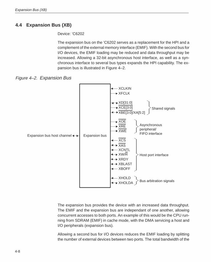
Expansion Bus (XB)
4-8
4.4 Expansion Bus (XB)
Device: ’C6202
The expansion bus on the ’C6202 serves as a replacement for the HPI and acomplement of the external memory interface (EMIF). With the second bus forI/O devices, the EMIF loading may be reduced and data throughput may beincreased. Allowing a 32-bit asynchronous host interface, as well as a syn-chronous interface to several bus types expands the HPI capability. The ex-pansion bus is illustrated in Figure 4–2.
Figure 4–2. Expansion Bus
Expansion bus
XCLKIN
Expansion bus host channel
XFCLK
XD[31:0]XCE[3:0]
XBE[3:0]/XA[5:2]
XOEXREXWE
XCS
XASXCNTLXW/RXRDYXBLASTXBOFF
XHOLDXHOLDA
Shared signals
Asynchronous peripheral/FIFO interface
Host port interface
Bus arbitration signals
The expansion bus provides the device with an increased data throughput.The EMIF and the expansion bus are independant of one another, allowingconcurrent accesses to both ports. An example of this would be the CPU run-ning from SDRAM (EMIF) in cache mode, with the DMA servicing a host andI/O peripherals (expansion bus).
Allowing a second bus for I/O devices reduces the EMIF loading by splittingthe number of external devices between two ports. The total bandwidth of the

Expansion Bus (XB)
4-9Peripherals
memory interfaces is increased, as transfers to and from the EMIF will notneed to be interrupted by peripheral or host servicing. The expansion bus alsoallows high-speed memories to be decoupled from lower speed devices.
The host-interface capability of the device is improved over the HPI. The ex-pansion bus offers two modes of operation: synchronous host and asynchro-nous host. The asynchronous host mode is a 32-bit version of the HPI. Thesynchronous mode allows an interface to several protocols:
� Master/slave PCI bridge interface
� Master/slave synchronous industry-standard host bus protocol
The expansion bus is serviced by the auxiliary channel of the DMA, and pro-vides a high data-transfer rate.
An example of a synchronous master/slave interface is shown in Figure 4–3,in which the device is interfaced to a i80960Jx chip.

Expansion Bus (XB)
4-10
Figure 4–3. Synchronous Interface
HOLD
HOLDA
CLKIN
XINT
BE_[3:0]
ADS_
AD[31:0]
READY
BLAST
W/R
i80960Jx
XHOLD
XHOLDA
XCLK
TOUT
XBE_[3:0]
XAS
XD[31:0]
XCNTL
XRDY
XBLAST
XW/R
XCS
TMS320C6202
32
4
CLOCK
Address
decoder
32
1
External Memory Interface (EMIF)
4-11Peripherals
4.5 External Memory Interface (EMIF)
Devices: all
The external memory interface (EMIF) supports a glueless interface to severalexternal devices, allowing additional data and program memory space beyondthat which is included on-chip. The types of memories supported include:
� Synchronous burst SRAM (SBSRAM)
� Synchronous DRAM (SDRAM)
� Asynchronous devices, including asynchronous SRAM, ROM, andFIFOs. The EMIF provides highly programmable timings to these inter-faces.
� External shared-memory devices
The EMIF is illustrated in Figure 4–4. Note that different devices of the ’C6000platform may combine some signals, and that you should consult the datasheet for a specific pin listing of the EMIF.

External Memory Interface (EMIF)
4-12
Figure 4–4. External Memory Interface (EMIF) Block Diagram
interfaceBus hold
interfaceSDRAM
interfaceSBSRAM
interfaceAsynchronous
interfacesall externalShared by
Program memory controller
Data memory controller
DMA
ÁÁÁÁÁÁÁÁÁÁÁÁÁÁÁÁÁÁÁÁÁÁÁÁÁÁÁÁÁÁÁÁÁÁÁÁÁÁÁÁÁÁÁÁÁÁÁÁÁÁÁÁÁÁÁÁÁÁÁÁÁÁÁÁÁÁÁÁÁÁÁÁÁÁÁÁÁÁÁÁÁÁÁÁÁÁÁÁÁÁÁÁÁÁÁÁÁÁÁÁÁÁÁÁÁÁÁÁÁÁÁÁÁÁÁÁÁÁÁÁÁÁÁÁÁÁÁÁÁÁÁÁÁÁÁÁÁÁÁÁÁÁÁÁÁÁÁ
(EMIF)interfacememoryExternal
HOLDA
HOLD
SDCLK
SDA10
SDWE
SDCAS
SDRAS
SSCLK
SSWE
SSOE
SSADS
ARE
AWE
AOE
ARDY
BE[3:0]
CE[3:0]
EA[21:2]
ED[31:0]
CLKOUT2
CLKOUT1
Internal peripheral bus
Controlregisters
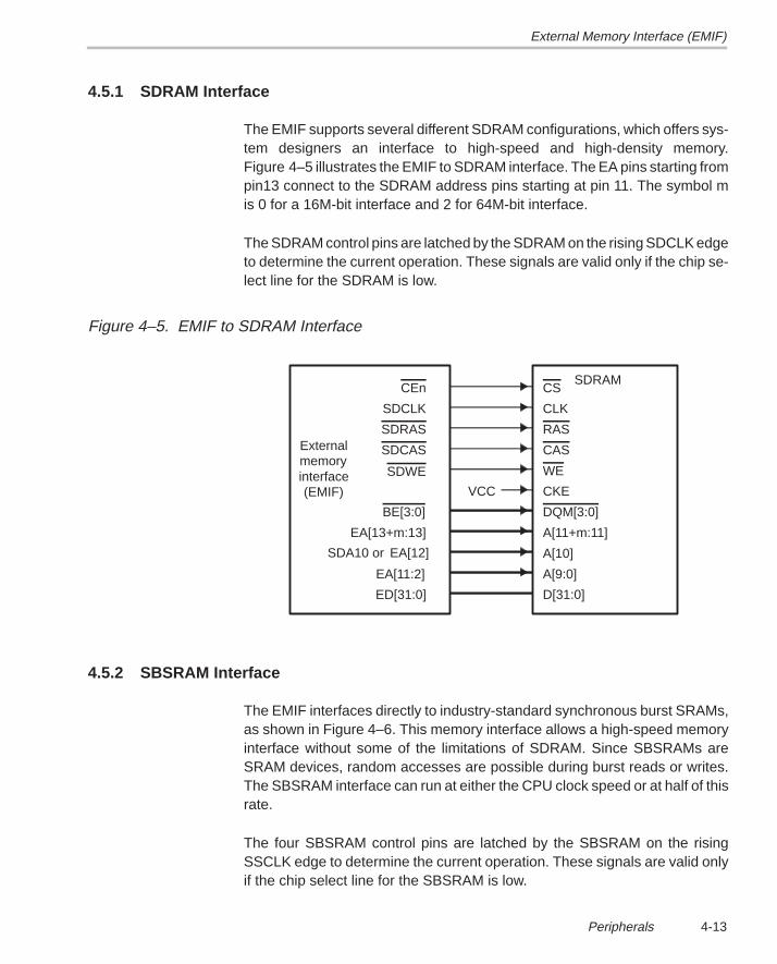
External Memory Interface (EMIF)
4-13Peripherals
4.5.1 SDRAM Interface
The EMIF supports several different SDRAM configurations, which offers sys-tem designers an interface to high-speed and high-density memory.Figure 4–5 illustrates the EMIF to SDRAM interface. The EA pins starting frompin13 connect to the SDRAM address pins starting at pin 11. The symbol mis 0 for a 16M-bit interface and 2 for 64M-bit interface.
The SDRAM control pins are latched by the SDRAM on the rising SDCLK edgeto determine the current operation. These signals are valid only if the chip se-lect line for the SDRAM is low.
Figure 4–5. EMIF to SDRAM Interface
VCC
SDRAM
D[31:0]
A[9:0]
A[10]
A[11+m:11]
DQM[3:0]
CKE
WE
CAS
RAS
CLK
CS
(EMIF)interfacememoryExternal
ED[31:0]
EA[11:2]
SDA10 or EA[12]
EA[13+m:13]
BE[3:0]
SDWE
SDCAS
SDRAS
SDCLK
CEn
4.5.2 SBSRAM Interface
The EMIF interfaces directly to industry-standard synchronous burst SRAMs,as shown in Figure 4–6. This memory interface allows a high-speed memoryinterface without some of the limitations of SDRAM. Since SBSRAMs areSRAM devices, random accesses are possible during burst reads or writes.The SBSRAM interface can run at either the CPU clock speed or at half of thisrate.
The four SBSRAM control pins are latched by the SBSRAM on the risingSSCLK edge to determine the current operation. These signals are valid onlyif the chip select line for the SBSRAM is low.
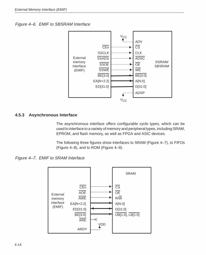
External Memory Interface (EMIF)
4-14
Figure 4–6. EMIF to SBSRAM Interface
SBSRAMSSRAM/
BE[3:0]BE[3:0]
D[31:0]
A[N:0]
WE
OE
ADSC
CLK
CS
(EMIF)interfacememoryExternal
ED[31:0]
EA[N+2:2]
SSWE
SSOE
SSADS
SSCLK
CEn
VCC
VCC
ADSP
ADV
4.5.3 Asynchronous Interface
The asynchronous interface offers configurable cycle types, which can beused to interface to a variety of memory and peripheral types, including SRAM,EPROM, and flash memory, as well as FPGA and ASIC devices.
The following three figures show interfaces to SRAM (Figure 4–7), to FIFOs(Figure 4–8), and to ROM (Figure 4–9).
Figure 4–7. EMIF to SRAM Interface
ARDY
ARE
SRAM
UB[1:0], LB[1:0]BE[3:0]
D[31:0]
A[N:0]
R/W
OE
CS
(EMIF)interfacememoryExternal
ED[31:0]
EA[N+2:2]
AWE
AOE
CEn
VDD

External Memory Interface (EMIF)
4-15Peripherals
Figure 4–8. EMIF to FIFO Interface
Tx FIFO
EN
D[31:0]
WRCLK/WRSTRB
Rx FIFO
AWE
RDCLK/RDSTRB
D[31:0]
OE
EN
(EMIF)interfacememoryExternal
ARE
ED[31:0]
EA[21:2]
AOE
CEn
ARDY
VDD
Figure 4–9. EMIF to ROM Interface
A[N:0]
ROM
ARDY
D[W-1:0]
OE
CS
(EMIF)interfacememoryExternal
ARE
ED[W-1:0]
EA[N+2:2]
AOE
CE1
VDD
The EMIF supports 8-, 16-, and 32-bit wide ROMs. In Figure 4–8, the W de-notes the number of data bits of the ROM. The memory-type field in the CEspace control register selects the access modes. In reading data from thesenarrow-width memory spaces, the EMIF packs multiple reads into one 32-bitwide value. This mode is primarily intended for word access to 8-bit and 16-bitROM devices.
For more specific memory interface descriptions, see the data sheet for theparticular ’C6000 device, as well as the TMS320C6201/C6701 PeripheralsReference Guide and the TMS320C6202/C6211 Peripherals ReferenceGuide Addendum.
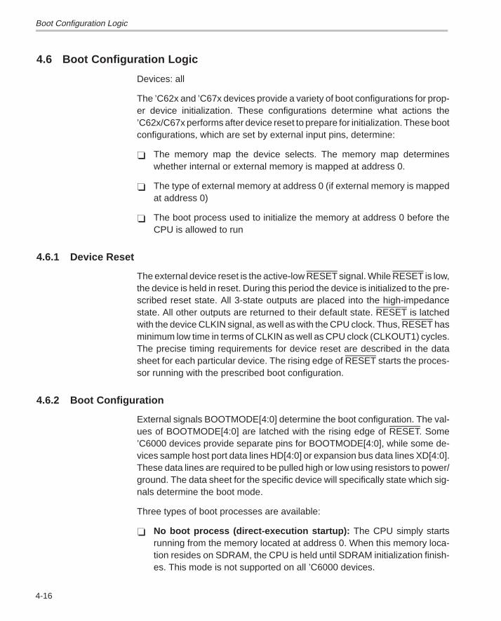
Boot Configuration Logic
4-16
4.6 Boot Configuration Logic
Devices: all
The ’C62x and ’C67x devices provide a variety of boot configurations for prop-er device initialization. These configurations determine what actions the’C62x/C67x performs after device reset to prepare for initialization. These bootconfigurations, which are set by external input pins, determine:
� The memory map the device selects. The memory map determineswhether internal or external memory is mapped at address 0.
� The type of external memory at address 0 (if external memory is mappedat address 0)
� The boot process used to initialize the memory at address 0 before theCPU is allowed to run
4.6.1 Device Reset
The external device reset is the active-low RESET signal. While RESET is low,the device is held in reset. During this period the device is initialized to the pre-scribed reset state. All 3-state outputs are placed into the high-impedancestate. All other outputs are returned to their default state. RESET is latchedwith the device CLKIN signal, as well as with the CPU clock. Thus, RESET hasminimum low time in terms of CLKIN as well as CPU clock (CLKOUT1) cycles.The precise timing requirements for device reset are described in the datasheet for each particular device. The rising edge of RESET starts the proces-sor running with the prescribed boot configuration.
4.6.2 Boot Configuration
External signals BOOTMODE[4:0] determine the boot configuration. The val-ues of BOOTMODE[4:0] are latched with the rising edge of RESET. Some’C6000 devices provide separate pins for BOOTMODE[4:0], while some de-vices sample host port data lines HD[4:0] or expansion bus data lines XD[4:0].These data lines are required to be pulled high or low using resistors to power/ground. The data sheet for the specific device will specifically state which sig-nals determine the boot mode.
Three types of boot processes are available:
� No boot process (direct-execution startup): The CPU simply startsrunning from the memory located at address 0. When this memory loca-tion resides on SDRAM, the CPU is held until SDRAM initialization finish-es. This mode is not supported on all ’C6000 devices.
Boot Configuration Logic
4-17Peripherals
� ROM boot process: A section of external memory is copied to address0 by the DMA/EDMA controller. Although the boot process begins whenthe device is released from external reset, this transfer occurs while theCPU is held in reset internally. The amount of memory copied is 16K wordsof 32 bits each. The width of the ROM is selected by BOOTMODE[4:3].In the case of ROM less than 32-bits wide, the EMIF can automaticallypack consecutive 8-bit bytes or 16-bit halfwords to form the 32-bit instruc-tion words to be moved. These values are expected to be stored in little-endian format in the external memory.
� Host-boot process: In the host-boot process, the CPU is held in resetwhile the remainder of the device is released from reset. During this peri-od, an external host can initialize the CPU’s memory space as necessarythrough the HPI or expansion bus, including external memory configura-tion registers. Once the necessary external memory has been configured,the host can access any external sections it needs to complete initializa-tion. After all necessary initialization, the host writes a 1 to the DSPINT bitin the HPI control register (HPIC). This write causes an active transitionon the DSPINT signal. In turn, this transition causes the boot configurationlogic to remove the CPU from its reset state. The CPU then begins runningfrom address 0. The CPU does not latch the DSPINT condition, becauseit occurs while the CPU is still in reset. Therefore the assertion will not reg-ister as an interrupt. Also, DSPINT wakes up the CPU from internal resetonly if the HPI boot process is selected.

Multichannel Buffered Serial Port (McBSP)
4-18
4.7 Multichannel Buffered Serial Port (McBSP)
Devices: all
The ’C62x/C67x multichannel buffered serial port (McBSP) is based on thestandard serial port interface found on the TMS320C2000 and ’C5000 plat-forms. The standard serial port interface provides:
� Full-duplex communication
� Double-buffered data registers, which allow a continuous data stream
� Independent framing and clocking for reception and transmission
� Direct interface to industry-standard codecs, analog interface chips(AICs), and other serially connected A/D and D/A devices
� External shift clock generation or an internal programmable frequencyshift clock
In addition, the McBSP has the following capabilities:
� Direct interface to:
� T1/E1 framers� MVIP and ST-BUS compliant devices� IOM-2 compliant devices� AC97 compliant devices� IIS compliant devices� SPI devices
� Multichannel transmission and reception of up to 128 channels.
� A wider selection of element sizes including 8-, 12-, 16-, 20-, 24-, or 32-bit
� µ-Law and A-Law companding
� 8-bit data transfers with LSB or MSB first
� Programmable polarity for both frame synchronization and data clocks
� Highly programmable internal clock and frame generation
The McBSP consists of a data path and control path. Seven pins connect thecontrol and data paths to external devices as shown in Figure 4–10.
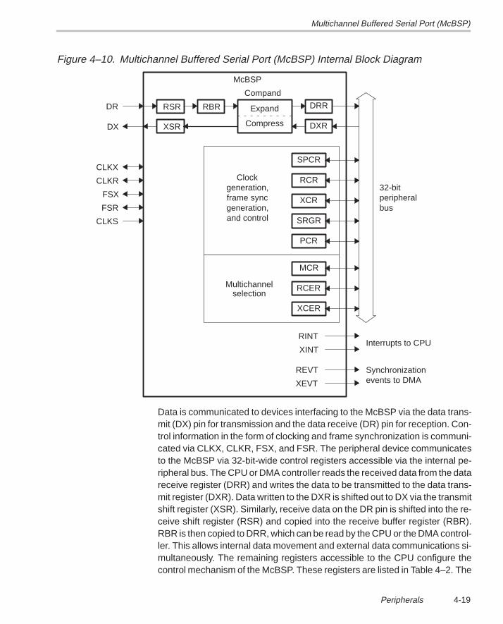
Multichannel Buffered Serial Port (McBSP)
4-19Peripherals
Figure 4–10. Multichannel Buffered Serial Port (McBSP) Internal Block Diagram
ÁÁÁÁÁÁÁÁÁÁÁÁÁÁÁÁÁÁÁÁÁÁÁÁÁÁÁÁÁÁÁÁÁÁÁÁÁÁÁÁÁÁÁÁÁÁÁÁÁÁÁÁÁÁÁÁÁÁÁÁÁÁÁÁÁÁÁÁÁÁÁÁÁÁÁÁÁÁÁÁÁÁÁÁÁÁÁÁÁÁÁÁÁÁÁÁÁÁÁÁÁÁÁÁÁÁÁÁÁÁÁÁÁÁÁÁÁÁÁÁÁÁÁÁÁÁÁÁÁÁÁÁÁÁÁÁÁÁÁÁÁÁÁÁÁÁÁÁÁÁÁÁÁÁÁÁÁÁÁÁÁÁÁÁÁÁÁÁÁÁÁÁÁÁÁÁÁÁÁÁÁÁÁÁÁÁÁÁÁÁÁÁÁÁÁÁÁÁÁÁÁÁÁÁÁÁÁÁÁÁÁÁÁÁÁÁÁÁÁÁÁÁÁÁÁÁÁÁÁÁÁÁÁÁÁÁÁÁÁÁÁÁÁÁÁÁÁÁÁÁÁÁÁÁÁÁÁÁÁÁÁÁÁÁÁÁÁÁÁÁÁÁÁÁÁÁÁÁÁÁÁÁÁÁÁÁÁÁÁÁÁÁÁÁÁÁÁÁÁÁÁÁÁÁÁÁÁÁÁÁÁÁÁÁÁÁÁÁÁÁÁÁÁÁÁÁÁÁÁÁÁÁÁÁÁÁÁÁÁÁÁÁÁÁÁ
ÁÁÁÁÁÁÁÁÁÁÁÁÁÁÁÁÁÁÁÁÁÁÁÁÁÁÁÁÁÁÁÁÁÁÁÁÁÁÁÁÁÁÁÁÁÁÁÁÁÁ
ÁÁÁÁÁÁÁÁÁÁÁÁÁÁÁÁÁÁÁÁÁÁÁÁÁÁÁÁÁÁÁÁÁÁÁÁÁÁÁÁÁÁÁÁÁÁÁÁÁÁÁÁÁÁÁÁÁÁÁÁÁÁÁÁÁÁÁÁÁÁÁÁÁÁÁÁÁÁÁÁÁÁÁÁÁÁÁÁÁÁ
ÁÁÁÁÁÁ
ÁÁÁÁÁÁ
ÁÁÁÁÁÁ
ÁÁÁÁÁÁ
ÁÁÁÁÁÁ
SRGR
ÁÁÁÁÁÁ
ÁÁÁÁÁÁ
ÁÁÁ
ÁÁÁÁÁÁ
ÁÁÁÁÁÁÁÁÁ
ÁÁÁ
ÁÁÁÁÁÁ
RBRÁÁÁÁÁÁ
ÁÁÁÁÁÁÁÁÁÁÁÁÁÁÁ
CLKS
FSR
FSX
CLKR
CLKX
DX
DR
XEVT
REVT
XINT
RINT
events to DMASynchronization
Interrupts to CPU
busperipheral32-bit
McBSP
Compand
XSR
RSR
Compress
Expand DRR
DXR
Multichannelselection
and controlgeneration,frame syncgeneration,
Clock
PCR
XCER
RCER
MCR
XCR
SPCR
RCR
Data is communicated to devices interfacing to the McBSP via the data trans-mit (DX) pin for transmission and the data receive (DR) pin for reception. Con-trol information in the form of clocking and frame synchronization is communi-cated via CLKX, CLKR, FSX, and FSR. The peripheral device communicatesto the McBSP via 32-bit-wide control registers accessible via the internal pe-ripheral bus. The CPU or DMA controller reads the received data from the datareceive register (DRR) and writes the data to be transmitted to the data trans-mit register (DXR). Data written to the DXR is shifted out to DX via the transmitshift register (XSR). Similarly, receive data on the DR pin is shifted into the re-ceive shift register (RSR) and copied into the receive buffer register (RBR).RBR is then copied to DRR, which can be read by the CPU or the DMA control-ler. This allows internal data movement and external data communications si-multaneously. The remaining registers accessible to the CPU configure thecontrol mechanism of the McBSP. These registers are listed in Table 4–2. The
Multichannel Buffered Serial Port (McBSP)
4-20
control block consists of internal clock generation, frame synchronization sig-nal generation, control for both of these, and multichannel selection. This con-trol block sends notification of important events to the CPU and the DMA con-troller via four signals as shown in Table 4–3.
Table 4–2. Multichannel Buffered Serial Port (McBSP) Registers
Abbreviation Register Name
RBR McBSP receive buffer register
RSR McBSP receive shift register
XSR McBSP transmit shift register
DRR McBSP data receive register
DXR McBSP data transmit register
SPCR McBSP serial port control register
RCR McBSP receive control register
XCR McBSP transmit control register
SRGR McBSP sample rate generator register
MCR McBSP multichannel register
RCER McBSP receive channel enable register
XCER McBSP transmit channel enable register
PCR McBSP pin control register
Table 4–3. Multichannel Buffered Serial Port (McBSP) CPU Interrupts andDMA Event Synchronization
Interrupt Name Description
RINT Receive interrupt to CPU
XINT Transmit Interrupt to CPU
REVT Receive synchronization event to DMA/EDMA
XEVT Transmit synchronization event to DMA/EDMA
Timers
4-21Peripherals
4.8 Timers
Devices: all
The ’C62x/C67x has two 32-bit general-purpose timers that you can use to:
� Time events� Count events� Generate pulses� Interrupt the CPU� Send synchronization events to the DMA controller
The timer has two signaling modes and can be clocked by an internal or anexternal source. The timer has an input pin (TINP) and an output pin (TOUT).The TINP pin can be used as a general-purpose input, and the TOUT pin canbe used as a general-purpose output.
With an internal clock, the timer can signal an external A/D converter to starta conversion, or it can trigger the DMA controller to begin a data transfer. Withan external clock, the timer can count external events and interrupt the CPUafter a specified number of events.
Interrupt Selector
4-22
4.9 Interrupt Selector
Devices: all
The ’C62x/C67x peripheral set produces 16 interrupt sources. The CPU has12 interrupts available for use. The interrupt selector allows you to choosewhich 12 of the 16 your system needs to use. The interrupt selector also allowsyou to effectively change the polarity of external interrupt inputs.
Table 4–4 lists the available interrupts.
Table 4–4. Peripheral Interrupts
InterruptSelectionNumber
InterruptAbbreviation
Interrupt Description
0000b DSPINT Host port host to DSP interrupt
0001b TINT0 Timer 0 interrupt
0010b TINT1 Timer 1 interrupt
0011b SD_INT EMIF SDRAM timer interrupt
0100b EXT_INT4 External interrupt pin 4
0101b EXT_INT5 External interrupt pin 5
0110b EXT_INT6 External interrupt pin 6
0111b EXT_INT7 External interrupt pin 7
1000b DMA_INT0/EDMA_INT DMA Ch0 interrupt / EDMA interrupt
1001b DMA_INT1 DMA Ch1 interrupt
1010b DMA_INT2 DMA Ch2 interrupt
1011b DMA_INT3 DMA Ch3 interrupt
1100b XINT0 McBSP 0 transmit interrupt
1101b RINT0 McBSP 0 receive Interrupt
1110b XINT1 McBSP 1 transmit interrupt
1111b RINT1 McBSP 1 receive interrupt

Power-Down Logic
4-23Peripherals
4.10 Power-Down Logic
Devices: all
Most of the operating power of CMOS logic is dissipated during circuit switch-ing, from one logic state to another. By preventing some or all of the chip’s logicfrom switching, significant power savings can be realized without losing anydata or operational context. Power-down mode PD1 blocks the internal clockinputs at the boundary of the CPU, preventing most of its logic from switching,effectively shutting down the CPU. Additional power savings are accom-plished in power-down mode PD2, in which the entire on-chip clock structure(including multiple buffers) is halted at the output of the PLL. Power-downmode PD3 shuts down the entire internal clock tree (like PD2) and also discon-nects the external clock source (CLKIN) from reaching the PLL. Wake-up fromPD3 takes longer than wake-up from PD2 because the PLL needs to be re-locked, just as it does following power up.
PD2 and PD3 assert the PD pin for external recognition of these two power-down modes. In addition to power-down modes, the IDLE instruction provideslower CPU power consumption by executing multiple NOPs. The IDLE instruc-tion terminates only upon servicing an interrupt.

5-1
Development Support
The TMS320C62x and TMS320C67x design environment reflects the uniquenature of the advanced VLIW architecture. The environment includes codegeneration tools, evaluation tools, documentation, online help with varioustools, and a web site on the Internet (http://www.ti.com/sc/docs/dsps/products/C6000) with complete technical documentation.
Topic Page
5.1 Code Generation Tools 5-2. . . . . . . . . . . . . . . . . . . . . . . . . . . . . . . . . . . . . . . .
5.2 Evaluation Tools 5-6. . . . . . . . . . . . . . . . . . . . . . . . . . . . . . . . . . . . . . . . . . . . . .
5.3 Third-Party Support 5-8. . . . . . . . . . . . . . . . . . . . . . . . . . . . . . . . . . . . . . . . . . .
5.4 Web Site and Documentation 5-10. . . . . . . . . . . . . . . . . . . . . . . . . . . . . . . . .
Chapter 5
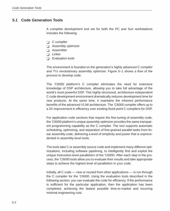
Code Generation Tools
5-2
5.1 Code Generation Tools
A complete development tool set for both the PC and Sun workstationsincludes the following:
� C compiler� Assembly optimizer� Assembler� Linker� Evaluation tools
The environment is founded on the generation’s highly advanced C compilerand TI’s revolutionary assembly optimizer. Figure 5–1 shows a flow of theprocess to develop code.
The ’C6000 platform’s C compiler eliminates the need for extensiveknowledge of DSP architecture, allowing you to take full advantage of theworld’s most powerful DSP. This highly-structured, architecture-independentC code development environment dramatically reduces development time fornew products. At the same time, it maintains the inherent performancebenefits of the advanced VLIW architecture. The ’C6000 compiler offers up toa 3X improvement in efficiency over existing fixed-point C compilers for DSP.
For application code sections that require the fine-tuning of assembly code,the ’C6000 platform’s unique assembly optimizer provides the same transpar-ent programming capability as the C compiler. The tool supports automaticscheduling, optimizing, and separation of fine-grained parallel tasks from lin-ear assembly code, delivering a level of simplicity and power that is unprece-dented in assembly-level tools.
The tools take C or assembly source code and implement many different opti-mizations, including software pipelining, to intelligently find and exploit theunique instruction-level parallelism of the ’C6000. After each step in the pro-cess, the ’C6000 tools allow you to evaluate their results and take appropriatesteps to achieve the highest level of parallelism in your code.
Initially, all C code –– new or reused from other applications –– is run throughthe C compiler for the ’C6000. Using the evaluation tools described in thefollowing section, you can evaluate the code for efficiency. If the performanceis sufficient for the particular application, then the application has beencompleted, achieving the fastest possible time-to-market and incurringminimal engineering cost.

Code Generation Tools
5-3Development Support
Figure 5–1. Code Development Flow Chart
Yes
No
Complete
Yes
No
Efficient?
Write C codePhase 1
Phase 2
Phase 3
More C optimizations?
No
Yes
No
Yes
Complete
Compile
Profile
Refine C code
Compile
Profile
Complete
Write linear assembly
Profile
Assembly optimize
Efficient?
Efficient?
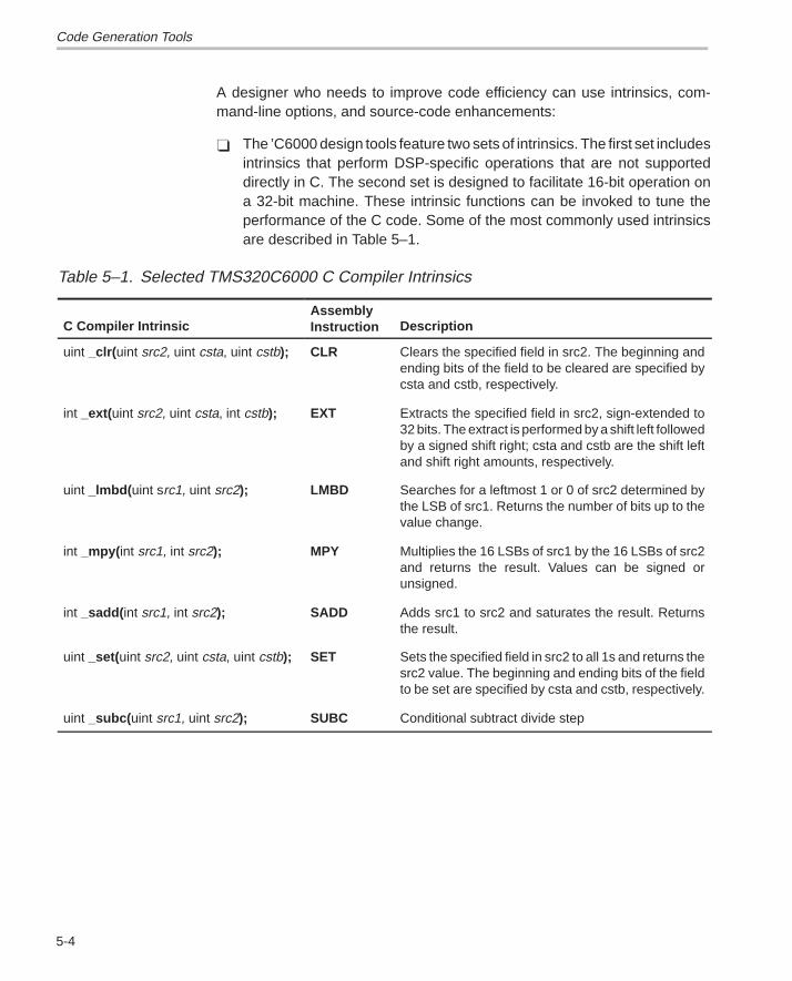
Code Generation Tools
5-4
A designer who needs to improve code efficiency can use intrinsics, com-mand-line options, and source-code enhancements:
� The ’C6000 design tools feature two sets of intrinsics. The first set includesintrinsics that perform DSP-specific operations that are not supporteddirectly in C. The second set is designed to facilitate 16-bit operation ona 32-bit machine. These intrinsic functions can be invoked to tune theperformance of the C code. Some of the most commonly used intrinsicsare described in Table 5–1.
Table 5–1. Selected TMS320C6000 C Compiler Intrinsics
C Compiler IntrinsicAssemblyInstruction Description
uint _clr( uint src2, uint csta, uint cstb); CLR Clears the specified field in src2. The beginning andending bits of the field to be cleared are specified bycsta and cstb, respectively.
int _ext(uint src2, uint csta, int cstb); EXT Extracts the specified field in src2, sign-extended to32 bits. The extract is performed by a shift left followedby a signed shift right; csta and cstb are the shift leftand shift right amounts, respectively.
uint _lmbd( uint src1, uint src2); LMBD Searches for a leftmost 1 or 0 of src2 determined bythe LSB of src1. Returns the number of bits up to thevalue change.
int _mpy( int src1, int src2); MPY Multiplies the 16 LSBs of src1 by the 16 LSBs of src2and returns the result. Values can be signed orunsigned.
int _sadd( int src1, int src2); SADD Adds src1 to src2 and saturates the result. Returnsthe result.
uint _set(uint src2, uint csta, uint cstb); SET Sets the specified field in src2 to all 1s and returns thesrc2 value. The beginning and ending bits of the fieldto be set are specified by csta and cstb, respectively.
uint _subc( uint src1, uint src2); SUBC Conditional subtract divide step

Code Generation Tools
5-5Development Support
� You can experiment with several command-line options that cause thecompiler to perform more aggressive optimization. One particularly usefuloption instructs the compiler to compile an entire application at once,giving the compiler visibility across program sections and more knowledgeof the way in which variables and functions are used. Another optioncauses the compiler to perform global optimizations across an entire ap-plication.
� Source-code enhancements can be made to exploit specific features ofthe ’C6000 architecture. For example, the ’C62x has support for operatingon words containing two 16-bit quantities; therefore, you can use 32-bitloads and stores when operating on arrays containing 16-bit data and eas-ily achieve a 2X performance improvement.
Taken together, these actions result in a large amount of parallelism in C code.
For ultra-high performance applications, extracting every last bit of throughputfrom the application code may be necessary. The profiler can identify criticalcode segments that might benefit most from being generated in assemblylanguage.
For these program sections, you write simple, linear ’C6000 assembly codethat is input to the assembly optimizer. This assembly code is ’C6000 instruc-tions written without concern for parallel instructions, instruction latencies, orregister usage.
The assembly optimizer tool schedules the instructions, taking into accountthe architectural parallelism. The tool honors ’C6000 latency requirements,maximizes parallel code, and performs register allocation.
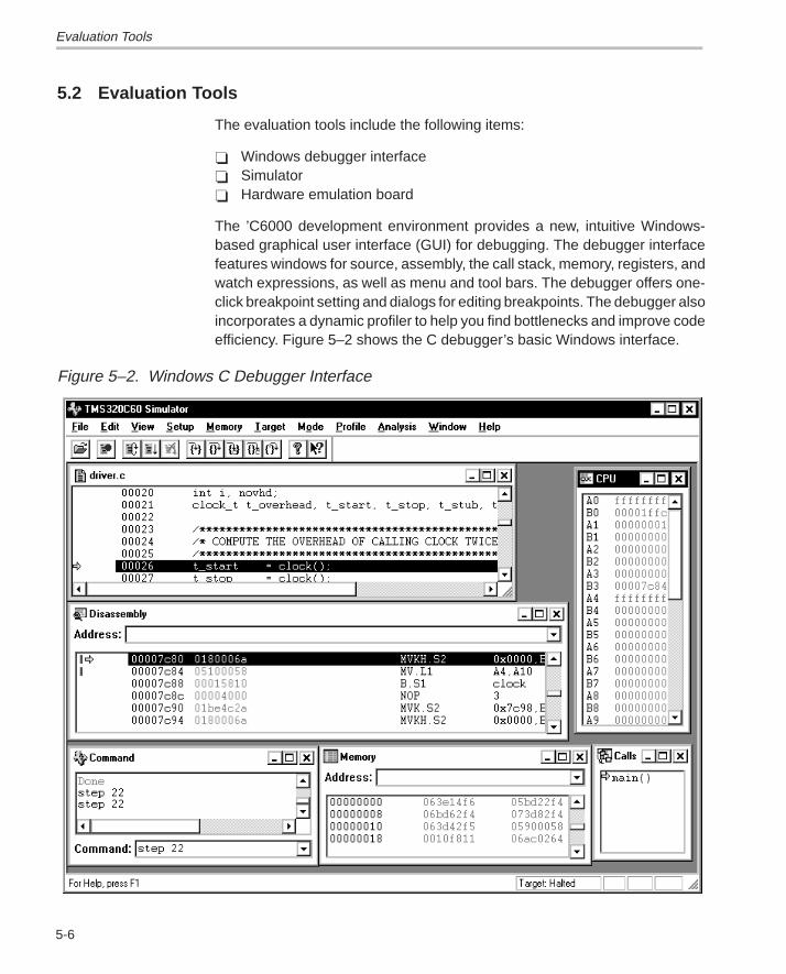
Evaluation Tools
5-6
5.2 Evaluation Tools
The evaluation tools include the following items:
� Windows debugger interface� Simulator� Hardware emulation board
The ’C6000 development environment provides a new, intuitive Windows-based graphical user interface (GUI) for debugging. The debugger interfacefeatures windows for source, assembly, the call stack, memory, registers, andwatch expressions, as well as menu and tool bars. The debugger offers one-click breakpoint setting and dialogs for editing breakpoints. The debugger alsoincorporates a dynamic profiler to help you find bottlenecks and improve codeefficiency. Figure 5–2 shows the C debugger’s basic Windows interface.
Figure 5–2. Windows C Debugger Interface
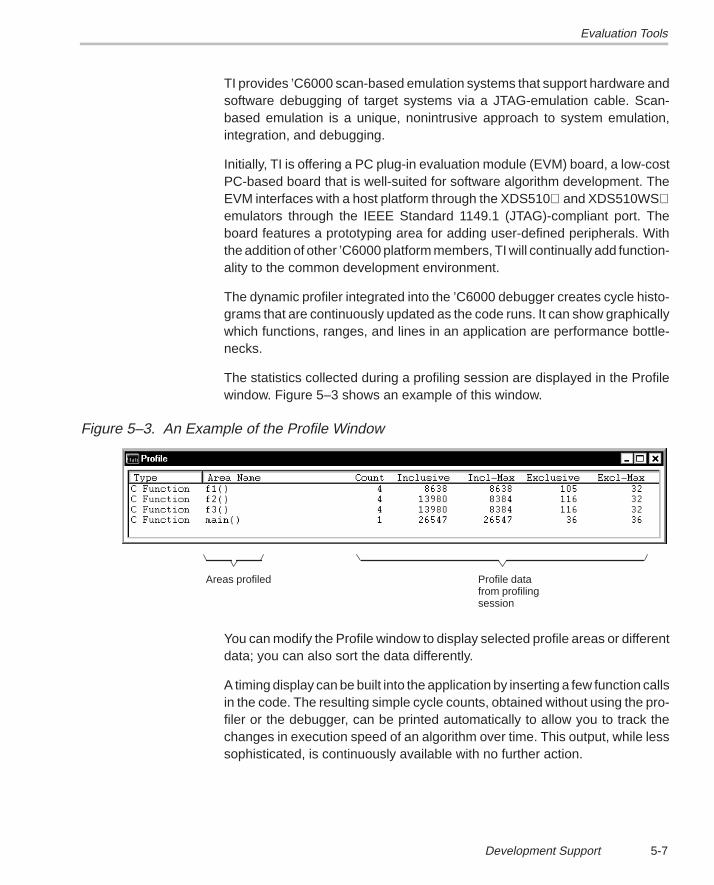
Evaluation Tools
5-7Development Support
TI provides ’C6000 scan-based emulation systems that support hardware andsoftware debugging of target systems via a JTAG-emulation cable. Scan-based emulation is a unique, nonintrusive approach to system emulation,integration, and debugging.
Initially, TI is offering a PC plug-in evaluation module (EVM) board, a low-costPC-based board that is well-suited for software algorithm development. TheEVM interfaces with a host platform through the XDS510 and XDS510WSemulators through the IEEE Standard 1149.1 (JTAG)-compliant port. Theboard features a prototyping area for adding user-defined peripherals. Withthe addition of other ’C6000 platform members, TI will continually add function-ality to the common development environment.
The dynamic profiler integrated into the ’C6000 debugger creates cycle histo-grams that are continuously updated as the code runs. It can show graphicallywhich functions, ranges, and lines in an application are performance bottle-necks.
The statistics collected during a profiling session are displayed in the Profilewindow. Figure 5–3 shows an example of this window.
Figure 5–3. An Example of the Profile Window
Profile datafrom profilingsession
Areas profiled
You can modify the Profile window to display selected profile areas or differentdata; you can also sort the data differently.
A timing display can be built into the application by inserting a few function callsin the code. The resulting simple cycle counts, obtained without using the pro-filer or the debugger, can be printed automatically to allow you to track thechanges in execution speed of an algorithm over time. This output, while lesssophisticated, is continuously available with no further action.

Third-Party Support
5-8
5.3 Third-Party Support
TI has a long history of strong third-party support and this continues with the’C62x/C67x devices. Table 5–2 lists the third-party contacts supporting the’C62x/C67x devices and their product areas with telephone numbers and elec-tronic mail addresses. For other contacts see out web site http://www.ti.com/sc/docs/dsps/develop/3party.htm
Table 5–2. Contacts for Third-Party Support
Third-Party Contact Product Area Phone Number e-mail Address
Ariel Corporation High-performance VME64 plat-form and computer telephonyproducts
609 860–2900 [email protected]
Cheops GmbH & CoKG
Industrial and medical imagingand high speed/high resolutionvideo conferencing
49 8861 2369 0 [email protected]
Commetrex DSP-resource boards andmedia-processing software
770 449–7775x310
D2 Technologies, Inc. Embedded Voice Processing(EVP ) computer telephonysoftware
805 564–3424 [email protected]
DNA Enterprises, Inc. DSP and telecom experienceproducts and design services
972 644–3301 [email protected]
D.SignT Standard credit-card-sizedDSP modules, developmenttools, system integration ser-vices
49 283 357 0977 adolf.klemenz@t–online.de
DSP Research, Inc. TIGER development boardsand OEM systems
408 773–1042 [email protected]
DSP Software Engineering, Inc.
Multichannel V.34bis modemand telecom software
617 275–3733 [email protected]
Eonic Systems, Inc. Real-time operating systems —Virtuoso Nano , Classico ,and MicroLite
301 572–5000 [email protected]
GO DSP Corporation Code Composer support andnext generation developmenttool, Code Maestro
416 599–6868 gdasilva@go–dsp.com
HotHaus Technologies,Inc.
HausWare — DSP softwarearchitecture for embedded tele-communications applications
604 278–4300 [email protected]
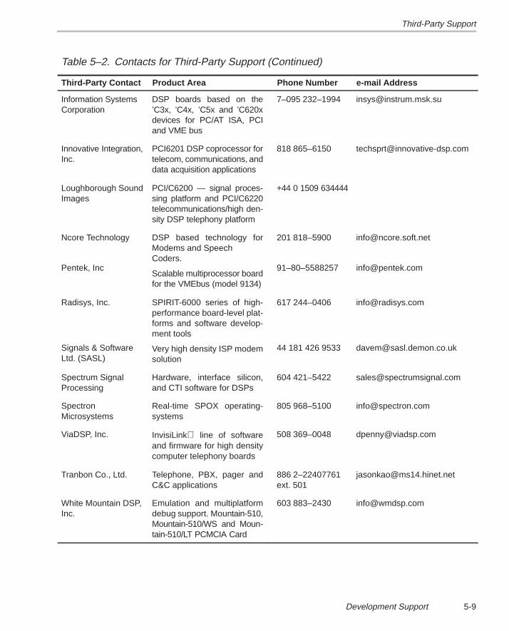
Third-Party Support
5-9Development Support
Table 5–2. Contacts for Third-Party Support (Continued)
Third-Party Contact e-mail AddressPhone NumberProduct Area
Information SystemsCorporation
DSP boards based on the’C3x, ’C4x, ’C5x and ’C620xdevices for PC/AT ISA, PCIand VME bus
7–095 232–1994 [email protected]
Innovative Integration,Inc.
PCI6201 DSP coprocessor fortelecom, communications, anddata acquisition applications
818 865–6150 [email protected]
Loughborough SoundImages
PCI/C6200 — signal proces-sing platform and PCI/C6220telecommunications/high den-sity DSP telephony platform
+44 0 1509 634444
Ncore Technology
Pentek, Inc
DSP based technology forModems and SpeechCoders.
Scalable multiprocessor boardfor the VMEbus (model 9134)
201 818–5900
91–80–5588257
Radisys, Inc.
Signals & SoftwareLtd. (SASL)
SPIRIT-6000 series of high-performance board-level plat-forms and software develop-ment tools
Very high density ISP modemsolution
617 244–0406
44 181 426 9533
Spectrum SignalProcessing
Hardware, interface silicon,and CTI software for DSPs
604 421–5422 [email protected]
SpectronMicrosystems
Real-time SPOX operating-systems
805 968–5100 [email protected]
ViaDSP, Inc. InvisiLink line of softwareand firmware for high densitycomputer telephony boards
508 369–0048 [email protected]
Tranbon Co., Ltd. Telephone, PBX, pager andC&C applications
886 2–22407761ext. 501
White Mountain DSP,Inc.
Emulation and multiplatformdebug support. Mountain-510,Mountain-510/WS and Moun-tain-510/LT PCMCIA Card
603 883–2430 [email protected]

Web Site and Documentation
5-10
5.4 Web Site and Documentation
Visit the web site at http://www.ti.com/sc/docs/dsps/products/C6000 forinformation, an interactive multimedia technical overview (MeTO),documentation, and a schedule of ’C6000 design workshops. MeTOdescribes features of the devices in a visual way, with graphics in apoint-and-click display for ease of navigation. The web site offers a completetraining schedule of design workshops and seminars. Applications assistanceand frequently asked questions (FAQ) are also on the web site.
Documentation is available directly from the web site in downloadable files forprinting. There is a complete list of documentation available in this book’sPreface under Related Documentation From Texas Instruments.

A-1
Appendix A
Glossary
A
address: The location of program code or data stored; an individually acces-sible memory location.
ALU: See arithmetic logic unit.
application-specific integrated circuit (ASIC): A custom chip designed fora specific application. It is designed by integrating standard cells from alibrary.
arithmetic logic unit (ALU): The hardware of the CPU that performs arith-metic and logic functions.
assembler: A software program that creates a machine-language programfrom a source file that contains assembly language instructions, direc-tives, and macro definitions. The assembler substitutes absolute opera-tion codes or relocatable codes for symbolic addresses.
assembly optimizer: A software program that optimizes linear assemblycode, which is assembly code that has not been register-allocated orscheduled. The assembly optimizer is automatically invoked with theshell program, cl6x, when one of the input files has an .sa extension.
ASIC: See application-specific integrated circuit.
B
boot: The process of loading a program into memory.
boot configuration: A set of parameters defining how a device is booted.
boot loader: A built-in segment of code that transfers code from an externalsource to program memory at power up.
Appendix A
Glossary
A-2
Ccache: A fast storage buffer in the central processing unit of a computer.
central processing unit (CPU): The unit that coordinates the functions ofa processor.
circular addressing: An address mode in which a finite set of addresses isreused by linking the largest address back to the smallest address.
clock cycles: A periodic or sequence of events based on the input from theexternal clock.
code: A set of instructions written to perform a task; a computer program orpart of a program.
compiler: A computer program that translates programs in a high-level lan-guage into their assembly-language equivalents.
control register: A register that contains bit fields which define the way adevice operates.
control register file: A set of control registers.
CPU: See central processing unit.
crosspath: A link between register files to provide communication betweenthe CPU units.
Ddata memory: A region of memory used for storing or manipulating data,
separate from the region used for storing program code.
direct memory access (DMA): Memory access that does not use the CPU;used for data transfer directly between memory and a peripheral.
direct memory access (DMA) controller: Specialized circuitry that trans-fers data from memory to memory without using the CPU.
DMA: See direct-memory access.
DRAM: See dynamic random-access memory.
dynamic random-access memory (DRAM): Memory that can be read andwritten by the microprocessor and whose storage locations can beaccessed in any order but must be refreshed (recharged) periodically toretain data or program code.

Glossary
A-3 Glossary
E
E1: A European high-speed network communication service that operatesat 2.048M bits per second and uses A-law companding.
erasable programmable read-only memory (EPROM): A memory devicewhose contents are erasable (usually via UV light) and programmable.
execute packet: A group of instructions that execute in parallel.
external interrupt: A hardware interrupt triggered by a pin.
external memory interface (EMIF): Microprocessor hardware which isused to read from and write to off-chip memory.
F
field programmable gate array (FPGA): An integrated circuit that containsan array of gates that can be programmed after manufacture, typicallyat the time of installation.
first-in, first-out (FIFO): A method for managing a set of items to whichadditions and deletions are made; items are added to one end of the listand removed from the other.
fixed-point processor: A processor which does arithmetic operationsusing integer arithmetic with no exponents.
flash memory: Electronically erasable, programmable nonvolatile (read-only) memory.
floating-point processor: A processor capable of handling floating-pointarithmetic where real operands are represented using exponents.
G
global interrupt enable bit (GIE): A bit in the control status register (CSR)that is used to enable or disable maskable interrupts.

Glossary
A-4
H
halfword: For this device, a halfword is defined as a 16-bit data item takenas a unit.
hardware interrupt: An interrupt triggered through physical connectionswith on-chip peripherals or external devices.
host port interface (HPI): A parallel interface that the CPU uses to commu-nicate with a host processor.
I
indirect addressing: An addressing mode in which an address points toanother pointer rather than to the actual data; this mode is prohibited inRISC architecture.
instruction fetch packet: A group of up to eight instructions held in memoryfor execution by the CPU.
interrupt: A signal sent by hardware or software to request a processor’sattention. An interrupt tells the processor to suspend its current opera-tion, save the current task status, and perform a particular set of instruc-tions. Interrupts communicate with the operating system and prioritizetasks to be performed.
interrupt service fetch packet (ISFP): A fetch packet used to service inter-rupts. If eight instructions are insufficient, the user must branch out of thisblock for additional interrupt servicing. If the delay slots of the branch donot reside within the ISFP, execution continues from execute packets inthe next fetch packet (the next ISFP).
L
latency: The delay between the occurrence of a condition and the reactionof the device. Also, in a pipeline, the necessary delay between the execu-tion of two potentially conflicting instructions to ensure that the valuesused by the second instruction are correct.
least significant bit (LSB): The lowest order bit in a word.
Glossary
A-5 Glossary
M
maskable interrupt : A hardware interrupt that can be enabled or disabledthrough software.
million instructions per second (MIPS): A measure of the executionspeed of a computer.
most significant bit (MSB): The highest order bit in a word.
multichannel buffered serial port (McBSP): An on-chip full-duplex circuitthat provides direct serial communication through several channels toexternal serial devices.
multiplexer: A device for selecting one of several available signals.
multiplier: A CPU component that multiplies the contents of two registers.
multivendor internet protocol: A standard network protocol supported byseveral major network communication vendors.
N
nonmaskable interrupt (NMI): An interrupt that can be neither masked nordisabled.
normalization: The reduction of a complex data structure to its simplestform or of a circuit to its lowest number of gates.
O
overflow: A condition in which the result of an arithmetic operation exceedsthe capacity of the register used to hold that result.

Glossary
A-6
P
packing: Minimizing the space occupied by data or memory through theelimination of discontinuous spaces between segments.
parallelism: Sequencing events to occur simultaneously. Parallelism isachieved in a CPU by using instruction pipelining.
peripheral: A device connected to and usually controlled by a host device.
pipeline: A method of executing instructions in which the output of one pro-cess serves as the input to another, much like an assembly line. Theseprocesses become the stages or phases of the pipeline.
pipeline processing: A technique that provides simultaneous, or parallel,processing within the computer. It refers to overlapping operations bymoving data or instructions into a conceptual pipe with all stages of thepipe processing simultaneously.
phase-locked loop (PLL): A circuit for synchronizing a variable oscillatorwith the phase of the transmitted signal.
program cache: A fast memory cache for storing program instructionsallowing for quick execution.
program fetch unit: The CPU hardware that retrieves program instructions.
program memory: A memory region used for storing and executingprograms, separate from the region used for storing data.

Glossary
A-7 Glossary
R
random-access memory (RAM): A type of memory device in which theindividual locations can be accessed in any order.
register: A small area of high speed memory, located within a processor orelectronic device, that is used for temporarily storing data or instructions.Each register is given a name, contains a few bytes of information, andis referenced by programs.
reduced-instruction set computer (RISC): A computer whose instructionset and related decode mechanism are much simpler than those ofmicroprogrammed complex instruction set computers. The result is ahigher instruction throughput and a faster real-time interrupt serviceresponse from a smaller, cost-effective chip.
reset: A means of bringing the CPU to a known state by setting the registersand control bits to predetermined values and signaling execution to startat a specified address.
S
saturation: A state where any further input no longer results in the expectedoutput.
synchronous burst static random-access memory (SBSRAM): RAMwhose content does not have to be refreshed periodically. Transfer ofdata is at a fixed rate relative to the clock speed of the device.
synchronous dynamic random-access memory (SDRAM): RAM whosecontent is refreshed periodically to prevent loss of the data. Transfer ofdata is at a fixed rate relative to the clock speed of the device.
shifter: A hardware unit that shifts bits in a word to the left or to the right.
T
T1: An American high-speed network communication service that runs at1.544M bits per second and uses µ-law companding.
Glossary
A-8
V
VelociTI: Architecture developed by TI that features very long instructionwords.
VLIW: Very long instruction word.
W
word: A set of bits (32 bits for the ’C6000 devices) that is stored, addressed,transmitted, or operated on as a unit.

Index
Index-1
Index
Aaddress paths 2-10
addressing mode register (AMR) 2-8, 2-18
addressing modescircular mode 2-18linear mode 2-18
applications 1-3assistance 5-8digital signal processors (DSPs) 1-3for the TMS320C6x 1-5TMS320 family 1-3
architectureCPU 2-1 to 2-13VelociTI 2-1
arithmetic logic unit (ALU) 2-3
auto modetypical C display 5-6
Bblock diagram
CPU core with peripherals 2-2external memory interface (EMIF) 4-12host port interface (HPI) 4-6multichannel buffered serial port (McBSP) 4-19TMS320C62x 2-2TMS320C67x 2-2
boot configuration 4-16 to 4-17
Ccentral processing unit (CPU) 1-2
addressing modes 2-18architecture 2-3
central processing unit (CPU) (continued)control register file 2-8control register file extensions 2-9core with peripherals 2-2data paths 2-4 to 2-10data paths figure
TMS320C62x 2-5TMS320C67x 2-6
data-address paths 2-10functional units 2-3, 2-7interrupts 2-19load and store paths 2-10memory paths 2-10register files 2-4
circular addressing 2-18block size specification 2-18
codedefinition A-2
code development flow chart 5-3code generation tools 5-2control registers
file extensions 2-9list of 2-8
control status register (CSR) 2-8CPU. See central processing unitcross paths 2-9
D.D functional units 2-7data paths 2-4
relationship to register files 2-9TMS320C62x 2-5TMS320C67x 2-6
data-address paths 2-10development support 5-2

Index
Index-2
development toolsC compiler 5-3code development flow 5-3
digital signal processors (DSPs) 1-1applications 1-3 to 1-4history 1-2performance progression 1-3
direct memory access (DMA) 2-2, 4-3 to 4-4, 4-21
DMA controller 4-3
EEMIF. See external memory interface (EMIF)
evaluation module (EVM) 5-7
evaluation tools 5-6
EVM. See evaluation module
Expansion Busblock diagram 4-8
external memory 3-11
external memory interface (EMIF) 2-2, 4-11 to 4-15asynchronous interface 4-14block diagram 4-12described 3-11in memory map 3-2interface to FIFO 4-15interface to ROM 4-15interface to SBSRAM 4-13interface to SDRAM 4-13interface to SRAM 4-14
Ffloating-point adder configuration register
(FADCR) 2-9
floating-point auxiliary configuration register(FAUCR) 2-9
floating-point multiplier configuration register(FMCR) 2-9
functional unit to instruction mapping 2-12
functional units 2-3, 2-7fixed-point operations 2-7floating-point operations 2-7list of 2-7mapping of instructions 2-11 to 2-17operations performed on 2-7
Ggeneral-purpose register files 2-4
cross paths 2-9data-address paths 2-10memory, load, and store paths 2-10
graphical user interface (GUI) 5-6
Hhost port interface (HPI) 4-6 to 4-7
block diagram 4-6boot process 4-6
Iinstruction fetch packet (IFP) 2-3
instruction to functional unit mapping 2-11
internal memory 3-4
interrupt clear register (ICR) 2-8
interrupt enable register (IER) 2-8
interrupt flag register (IFR) 2-8
interrupt return pointer (IRP) 2-8
interrupt selector 4-22
interrupt service table pointer (ISTP) 2-8
interrupt set register (ISR) 2-8
interrupts 2-19
intrinsics 5-4
introductionTMS320 family overview 1-2TMS320C62x 1-5TMS320C67x 1-5
L.L functional units 2-7, 2-9
linear addressing mode 2-18
load address generationsyntax 2-18
load and store pathsCPU 2-10
load instructionssyntax for indirect addressing 2-18
load paths 2-10
Index
Index-3
M.M functional units 2-7, 2-9mapping
functional unit to instruction 2-12instruction to functional unit 2-11
memoryexternal 3-11external memory interface (EMIF) 3-11, 4-11internal 3-4map 3-2, 3-3paths 2-10
memory map 3-2memory paths 2-10multichannel buffered serial port (McBSP) 4-18 to
4-20block diagram 4-19CPU interrupts 4-20DMA events 4-20registers 4-20
Nnonmaskable interrupt (NMI) 2-19nonmaskable interrupt return pointer (NRP) 2-8
Ooverview
TMS320 family 1-2
PPD1–PD3 4-23performance progression of DSPs 1-3peripherals 4-1
direct-memory access (DMA) 4-3external memory interface (EMIF) 4-11host port interface (HPI) 4-6interrupts 4-22multichannel buffered serial port (McBSP) 4-18timers 4-21
pipelinedefinition A-6
pipeline processingdefinition A-6
power-down logic 4-23power-down modes 4-23program counter (PCE1) 2-8
Rregister files 2-4
cross paths 2-9data-address paths 2-10memory, load, and store paths 2-10relationship to data paths 2-9
resetand boot configuration 4-16definition A-7
ROM modes for external memory interface 4-11
S.S functional units 2-7store address generation
syntax 2-18store instructions
syntax for indirect addressing 2-18store paths 2-10synchronous burst static RAM 3-11Synchronous interface
block diagram 4-10
Tthird-party support
contacts 5-8TMS320 family
advantages 1-2applications 1-3 to 1-4characteristics 1-2development 1-2history 1-2introduction to the ’C6x 1-5overview 1-2performance progression 1-3
TMS320C62x devicesblock diagram 2-2CPU data paths 2-5features 1-6options 1-6 to 1-8performance 1-5
TMS320C67x devicesblock diagram 2-2CPU data paths 2-6features 1-6options 1-6 to 1-8performance 1-5

Index
Index-4
toolsassembler 5-2assembly optimizer 5-2C compiler 5-2debugger 5-6evaluation 5-6evaluation tools 5-2hardware emulation board 5-6linker 5-2simulator 5-6tool set 5-2
Uusing the C compiler 5-3
VVelociTI architecture 1-1, 2-1VLIW (very long instruction word) architecture 1-1
Wweb site 5-10
Related Documents