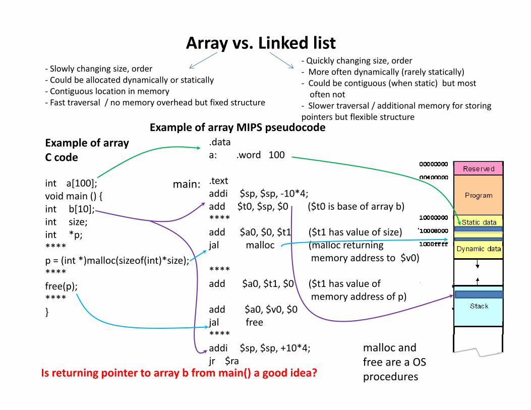
Array vs. Linked list ‐ Quickly changing size, order ‐ More often dynamically(rarely statically) ‐ Slowly changing size, order ‐ Could be contiguous (when static) but most often not ‐ Slower traversal / additional memory for storing pointers but flexible structure ‐ Could be allocated dynamically or statically ‐ Contiguous location in memory ‐ Fast traversal / no memory overhead but fixed structure Example of array MIPS pseudocode [ ] .data a: .word 100 text Example of array C code Example of array MIPS pseudocode int a[100]; void main () { int b[10]; int size; * . text addi $sp, $sp, ‐10*4; add $t0, $sp, $0 ($t0 is base of array b) **** add $a0 $0 $t1 ($t1 has value of size) main: int *p; **** p = (int *)malloc(sizeof(int)*size); **** f () add $a0, $0, $t1 ($t1 has value of size) jal malloc (malloc returning memory address to $v0) **** add $a0 $t1 $0 ($t1 has value of free(p); **** } add $a0, $t1, $0 ($t1 has value of memory address of p) add $a0, $v0, $0 jal free **** **** addi $sp, $sp, +10*4; jr $ra malloc and free are a OS procedures Is returning pointer to array b from main() a good idea?

Welcome message from author
This document is posted to help you gain knowledge. Please leave a comment to let me know what you think about it! Share it to your friends and learn new things together.
Transcript
Array vs. Linked list‐ Quickly changing size, order‐ More often dynamically (rarely statically)‐ Slowly changing size, order y y ( y y)‐ Could be contiguous (when static) but most often not
‐ Slower traversal / additional memory for storing pointers but flexible structure
‐ Could be allocated dynamically or statically‐ Contiguous location in memory ‐ Fast traversal / no memory overhead but fixed structure
Example of array MIPS pseudocode
[ ]
.dataa: .word 100
text
Example of array C code
Example of array MIPS pseudocode
int a[100];void main () {int b[10];int size;
*
.textaddi $sp, $sp, ‐10*4;add $t0, $sp, $0 ($t0 is base of array b)****add $a0 $0 $t1 ($t1 has value of size)
main:
int *p;****p = (int *)malloc(sizeof(int)*size);****f ( )
add $a0, $0, $t1 ($t1 has value of size)jal malloc (malloc returning
memory address to $v0)****add $a0 $t1 $0 ($t1 has value offree(p);
****}
add $a0, $t1, $0 ($t1 has value of memory address of p)
add $a0, $v0, $0jal free********addi $sp, $sp, +10*4;jr $ra
malloc and free are a OS procedures Is returning pointer to array b from main() a good idea?
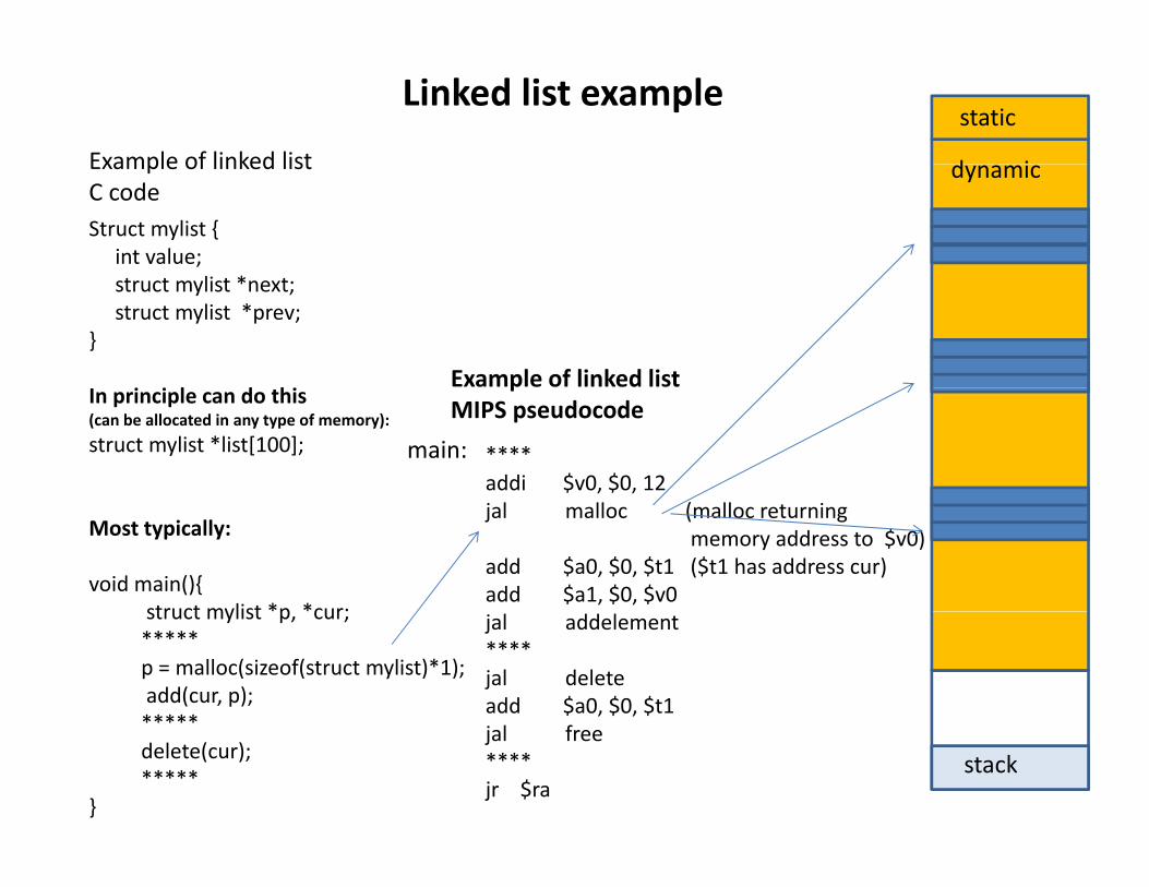
Example of linked list
Linked list example
d i
static
Struct mylist {int value;
l *
Example of linked list C code
dynamic
struct mylist *next;struct mylist *prev;
}
i i l d hiExample of linked list
In principle can do this(can be allocated in any type of memory):
struct mylist *list[100]; ****addi $v0, $0, 12
pMIPS pseudocode
main:
Most typically:
void main(){struct mylist *p *cur;
jal malloc (malloc returning memory address to $v0)
add $a0, $0, $t1 ($t1 has address cur)add $a1, $0, $v0
struct mylist p, cur;*****p = malloc(sizeof(struct mylist)*1);add(cur, p);*****
jal addelement****jal deleteadd $a0, $0, $t1
delete(cur);*****
}
jal free****jr $ra
stack
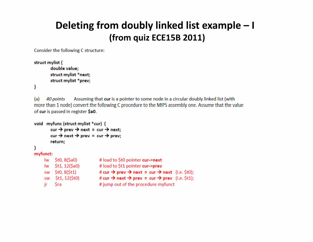
Deleting from doubly linked list example – I(from quiz ECE15B 2011)
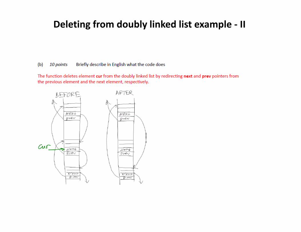
Deleting from doubly linked list example ‐ II
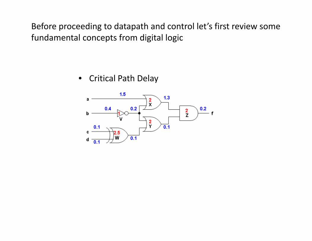
Before proceeding to datapath and control let’s first review some fundamental concepts from digital logic
l h l• Critical Path Delay
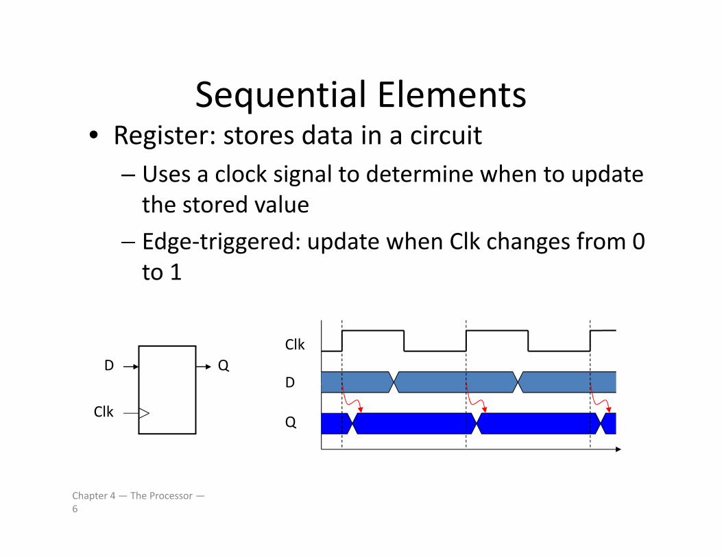
Sequential ElementsSequential Elements• Register: stores data in a circuit
Uses a clock signal to determine when to update– Uses a clock signal to determine when to update the stored value
– Edge‐triggered: update when Clk changes from 0Edge‐triggered: update when Clk changes from 0 to 1
D QClk
D
Clk
D
Q
Chapter 4 — The Processor —6
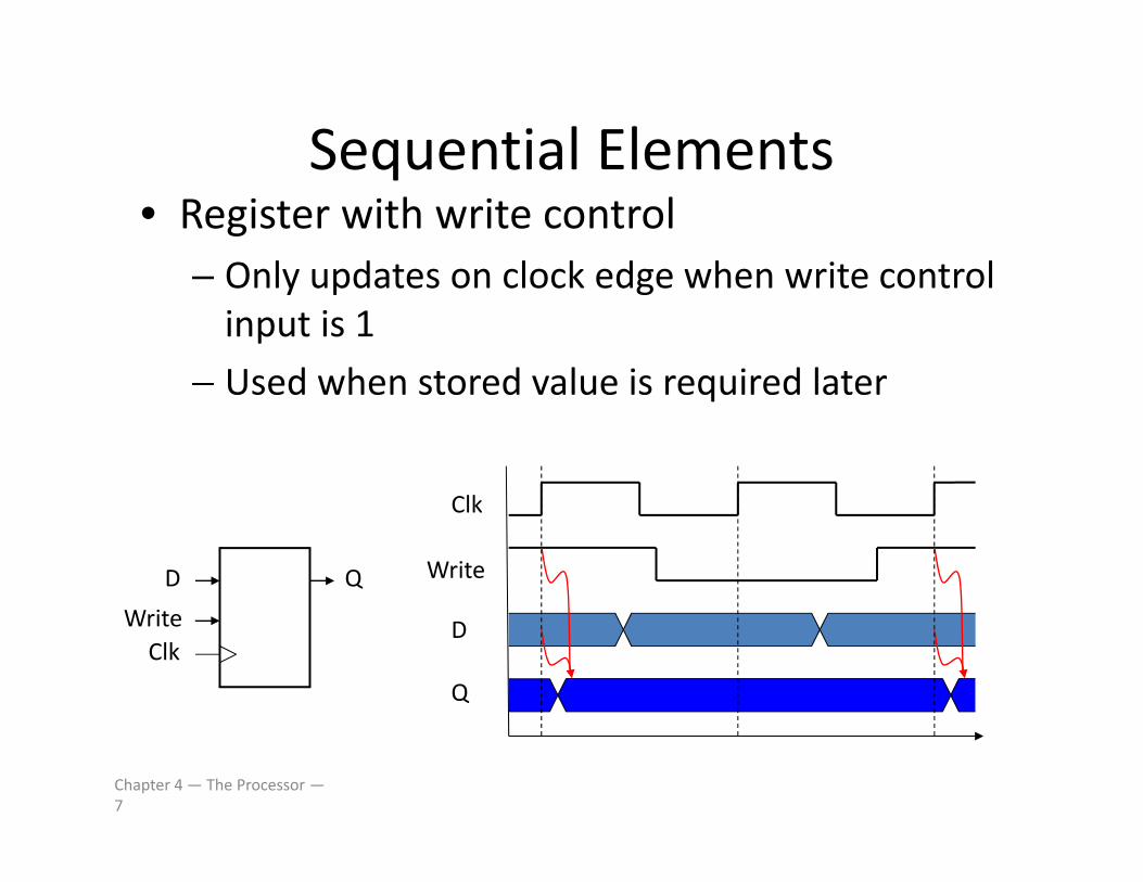
Sequential ElementsSequential Elements• Register with write control
Only updates on clock edge when write control– Only updates on clock edge when write control input is 1
– Used when stored value is required laterUsed when stored value is required later
Clk
D Q Write
Clk
ClkWrite D
Q
Chapter 4 — The Processor —7
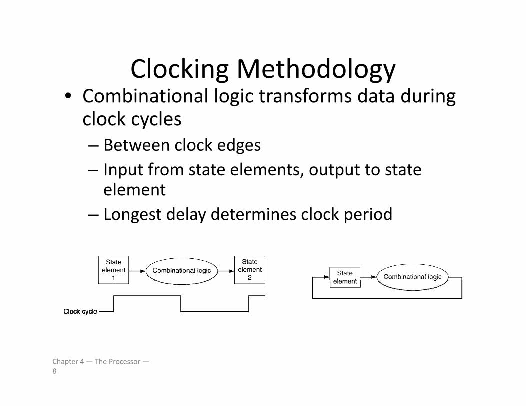
Clocking MethodologyClocking Methodology• Combinational logic transforms data during clock cyclesy– Between clock edges– Input from state elements, output to state p , pelement
– Longest delay determines clock period
Chapter 4 — The Processor —8
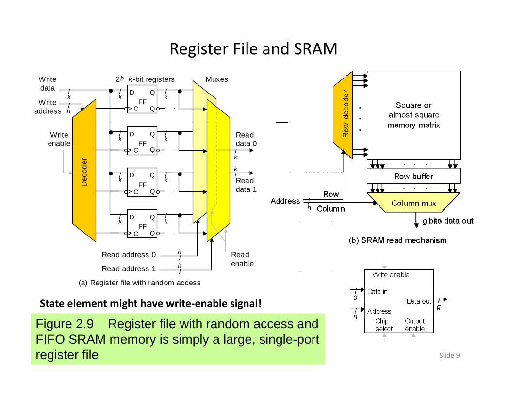
Register File and SRAM
/ k
Write data
2 k -bit registersh / k
/ k
/ h
Write address
Muxes
/ k /
Write enable
/ k
Write data Write
Read data 0
Q C
Q
D FF
oder
/ k
Write enable
Read data 0
/ k
/ k
k
/ h / h
/ h
Read addr 0
/ k
Read addr 1
addr
Read enable
Read data 1
Q C
Q
D FF
Dec
o / k
/ k
/ k
Read data 1
/
Read enable
(b) Graphic symbol for register file
Q D
/ k
Q C
Q
D FF
/
h Read address 0
Read address 1
Read enable
k
k
/h
C
Q
FF
/ k
Push
/ k
Input
Output Pop
Full
Empty
Fig re 2 9 Register file ith random access andState element might have write‐enable signal!
/ (a) Register file with random access (c) FIFO symbol
Jan. 2011Computer Architecture, Background and
MotivationSlide 9
Figure 2.9 Register file with random access and FIFO SRAM memory is simply a large, single-port register file
Single Cycle DatapathSingle Cycle Datapath
• General AssumptionsGeneral Assumptions– One instruction executed per one cycle
State elements are updated only at the end of– State elements are updated only at the end of cycle
– Control and data signals (after they become– Control and data signals (after they become stable) does not change during cycle
• Two addition operations during cycle = two physical p g y p yadders (however still want to share resources among instructions as much as possible – e.g. by using muxes)
Introduction§4.1 IntroIntroduction
• CPU performance factors
oduction
– Instruction count• Determined by ISA and compiler
– CPI and Cycle time• Determined by CPU hardware
• We will examine two MIPS implementations– A simplified version– A more realistic pipelined version
• Simple s bset sho s most aspects• Simple subset, shows most aspects– Memory reference: lw, sw– Arithmetic/logical: add, sub, and, or, slt– Control transfer: beq, jo o a s e beq, j
Note that datapath from P&H (which is simpler) is discussed in details in class while datapathfrom BP is given as a reference
Chapter 4 — The Processor —11
g
Instruction ExecutionInstruction Execution
• PC instruction memory, fetch instructionPC instruction memory, fetch instruction
• Register numbers register file, read registers• Depending on instruction classDepending on instruction class
– Use ALU to calculate• Arithmetic result
• Memory address for load/store
• Branch target address
Access data memory for load/store– Access data memory for load/store
– PC target address or PC + 4
Chapter 4 — The Processor —12
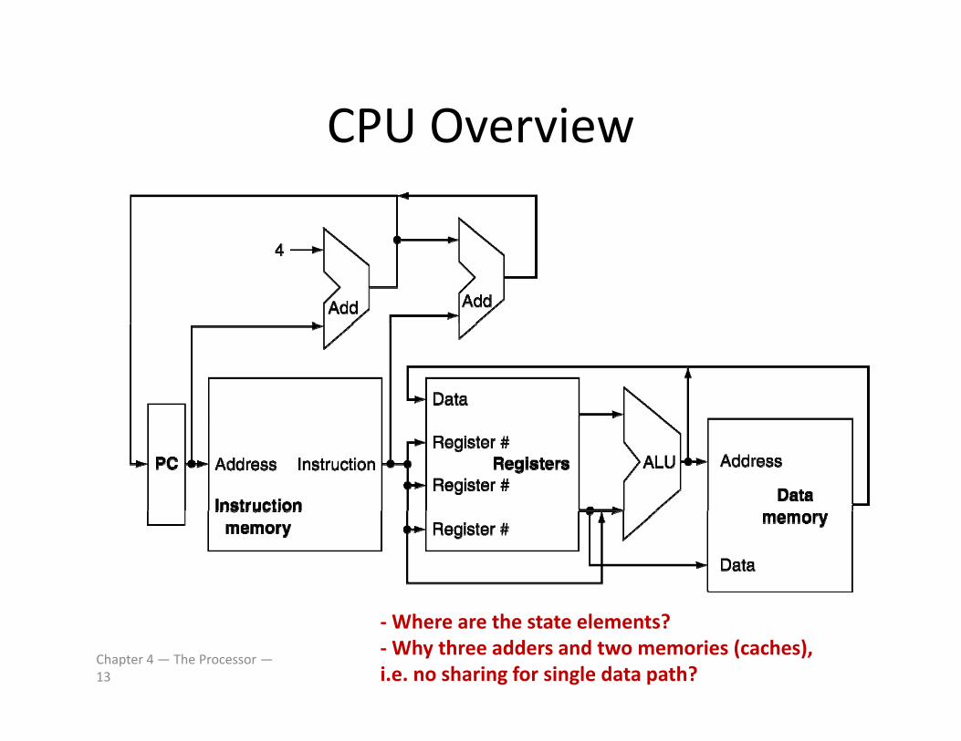
CPU OverviewCPU Overview
Chapter 4 — The Processor —13
‐Where are the state elements?‐Why three adders and two memories (caches), i.e. no sharing for single data path?
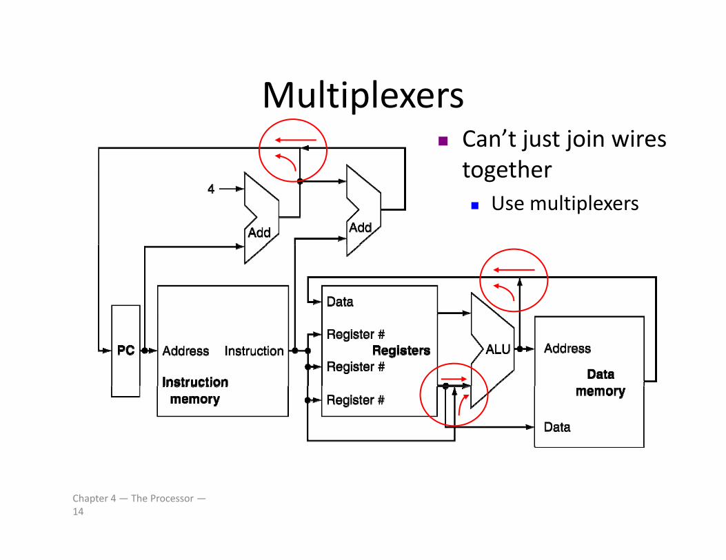
MultiplexersMultiplexers Can’t just join wires togethertogether Use multiplexers
Chapter 4 — The Processor —14
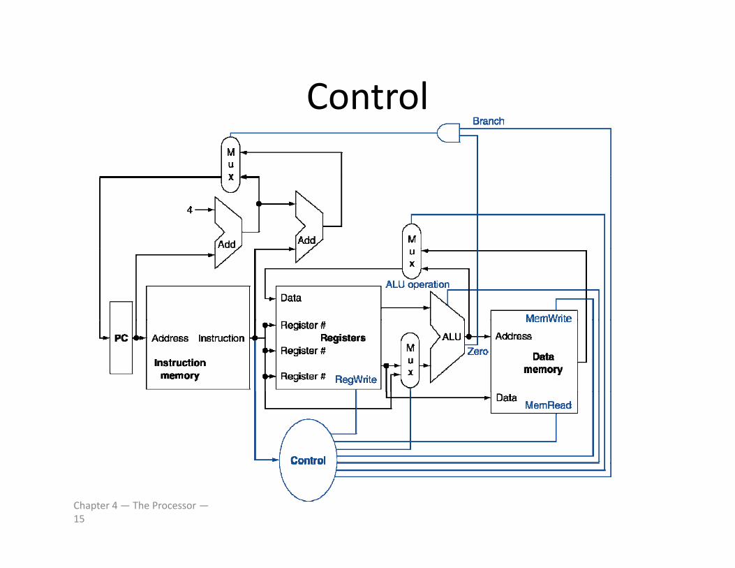
ControlControl
Chapter 4 — The Processor —15
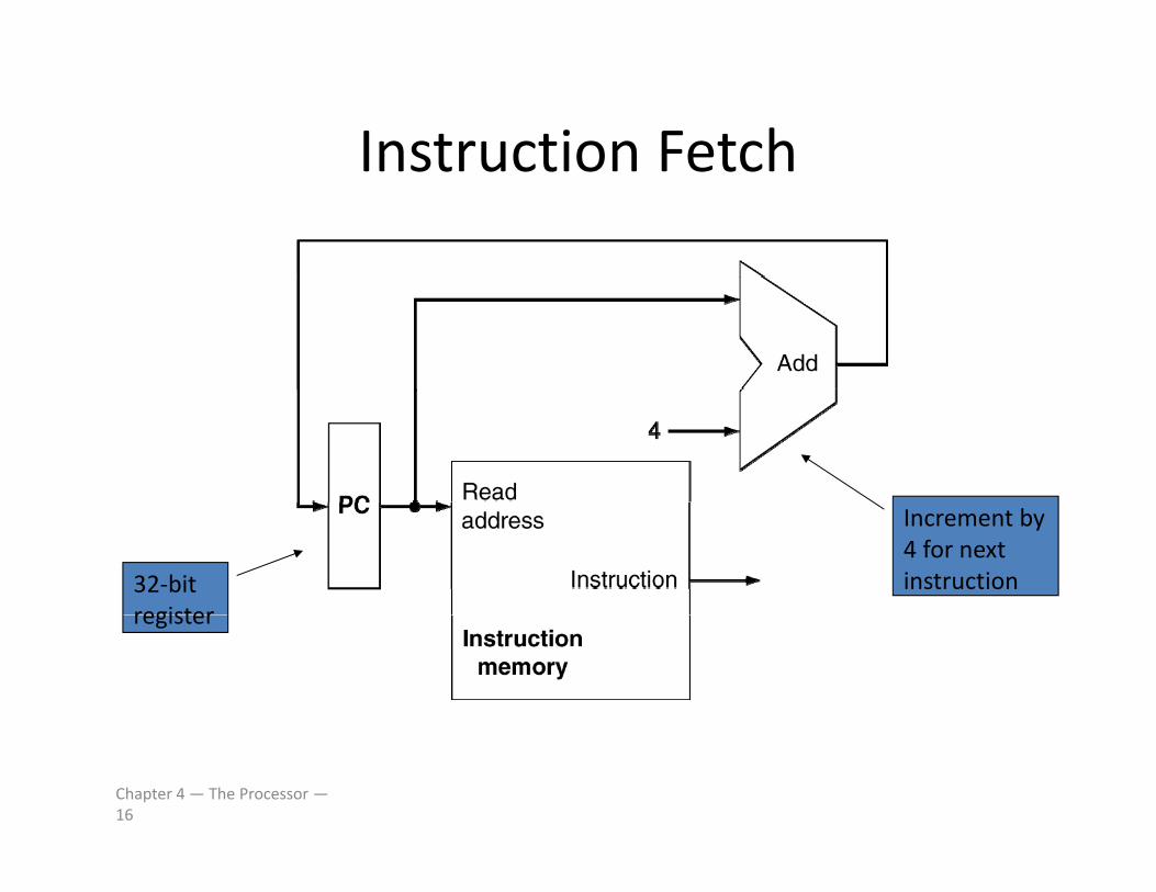
Instruction FetchInstruction Fetch
32‐bit register
Increment by 4 for next instruction
register
Chapter 4 — The Processor —16
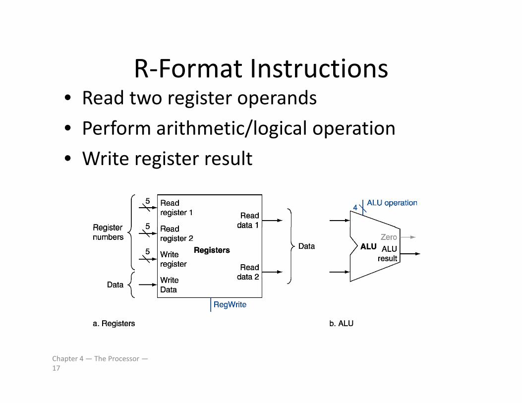
R‐Format InstructionsR Format Instructions• Read two register operands
• Perform arithmetic/logical operation• Perform arithmetic/logical operation
• Write register result
Chapter 4 — The Processor —17
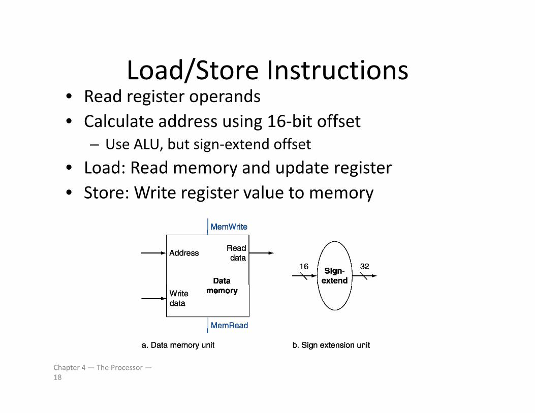
Load/Store InstructionsLoad/Store Instructions• Read register operands• Calculate address using 16‐bit offsetg
– Use ALU, but sign‐extend offset
• Load: Read memory and update register• Store: Write register value to memory
Chapter 4 — The Processor —18
Branch InstructionsBranch Instructions
• Read register operandsRead register operands
• Compare operandsU ALU bt t d h k Z t t– Use ALU, subtract and check Zero output
• Calculate target address– Sign‐extend displacement
– Shift left 2 places (word displacement)
– Add to PC + 4• Already calculated by instruction fetch
Chapter 4 — The Processor —19
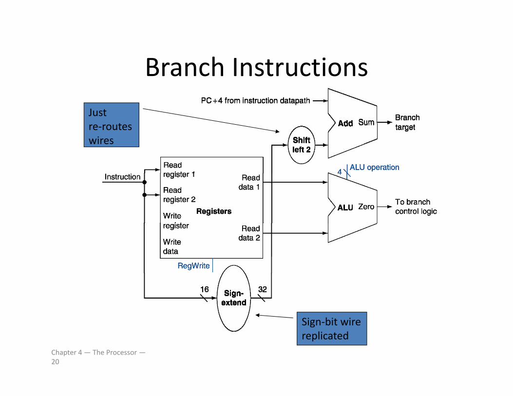
Branch InstructionsBranch InstructionsJust
tre‐routes wires
Sign‐bit wire
Chapter 4 — The Processor —20
Sign bit wire replicated
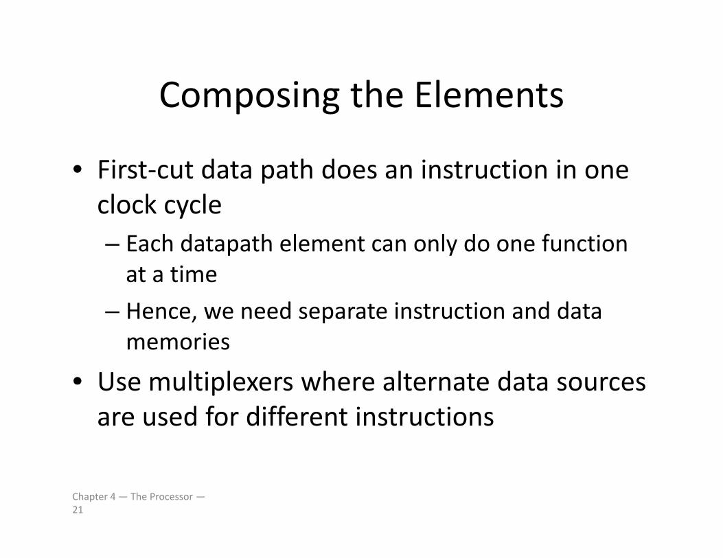
Composing the ElementsComposing the Elements
• First‐cut data path does an instruction in oneFirst cut data path does an instruction in one clock cycle– Each datapath element can only do one function– Each datapath element can only do one function at a time
– Hence we need separate instruction and dataHence, we need separate instruction and data memories
• Use multiplexers where alternate data sourcesUse multiplexers where alternate data sources are used for different instructions
Chapter 4 — The Processor —21
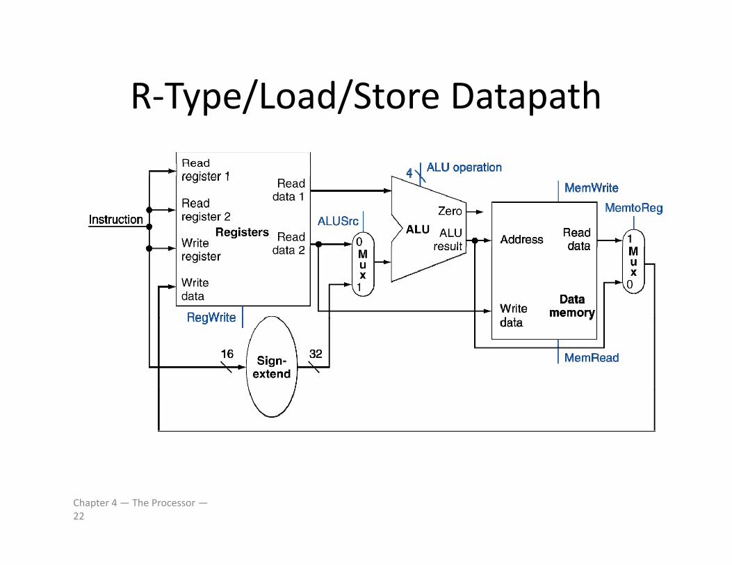
R‐Type/Load/Store DatapathR Type/Load/Store Datapath
Chapter 4 — The Processor —22
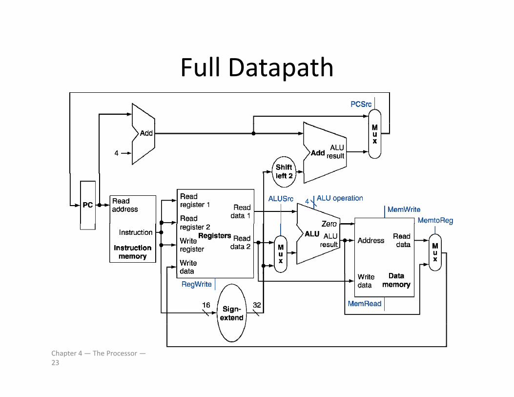
Full DatapathFull Datapath
Chapter 4 — The Processor —23
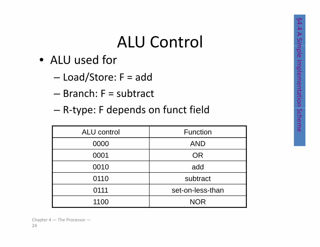
ALU Control§4.4 A
SimALU Control• ALU used for
Load/Store: F = add
mple Im
plem– Load/Store: F = add
– Branch: F = subtract
R type F depends on funct field
mentation – R‐type: F depends on funct field Schem
e
ALU control Function0000 AND0001 OR0010 add0110 subtract0111 set-on-less-than1100 NOR
Chapter 4 — The Processor —24
1100 NOR
ALU ControlALU Control
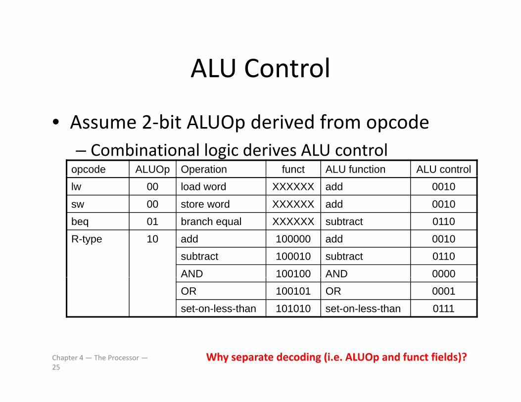
• Assume 2‐bit ALUOp derived from opcodeAssume 2 bit ALUOp derived from opcode– Combinational logic derives ALU control
opcode ALUOp Operation funct ALU function ALU controllw 00 load word XXXXXX add 0010sw 00 store word XXXXXX add 0010beq 01 branch equal XXXXXX subtract 0110q qR-type 10 add 100000 add 0010
subtract 100010 subtract 0110AND 100100 AND 0000AND 100100 AND 0000OR 100101 OR 0001set-on-less-than 101010 set-on-less-than 0111
Chapter 4 — The Processor —25
Why separate decoding (i.e. ALUOp and funct fields)?
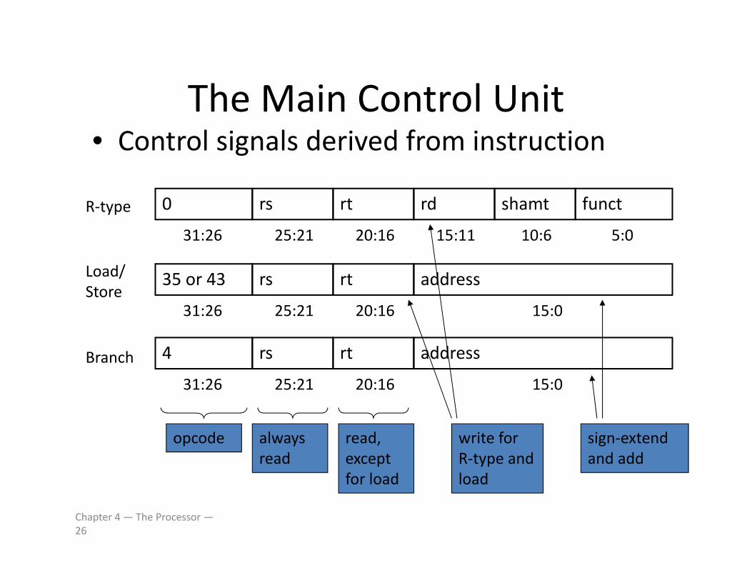
The Main Control UnitThe Main Control Unit• Control signals derived from instruction
0 rs rt rd shamt funct
31:26 5:025:21 20:16 15:11 10:6
R‐type
35 or 43 rs rt address
31:26 25:21 20:16 15:0
Load/Store
4 rs rt address
31:26 25:21 20:16 15:0
Branch
opcode always read
read, except f l d
write for R‐type and l d
sign‐extend and add
Chapter 4 — The Processor —26
for load load
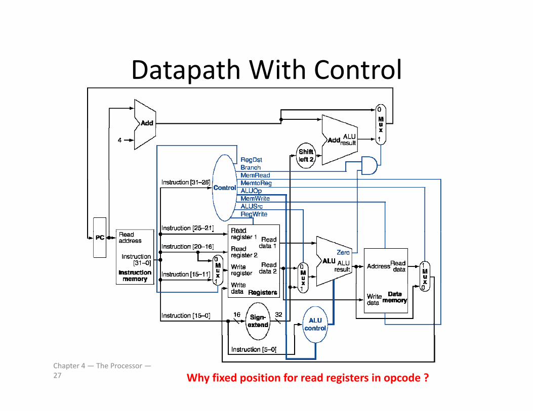
Datapath With ControlDatapath With Control
Chapter 4 — The Processor —27 Why fixed position for read registers in opcode ?
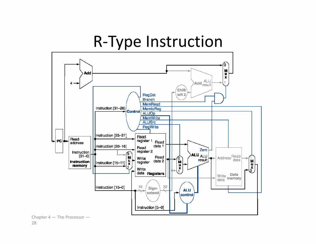
R‐Type InstructionR Type Instruction
Chapter 4 — The Processor —28
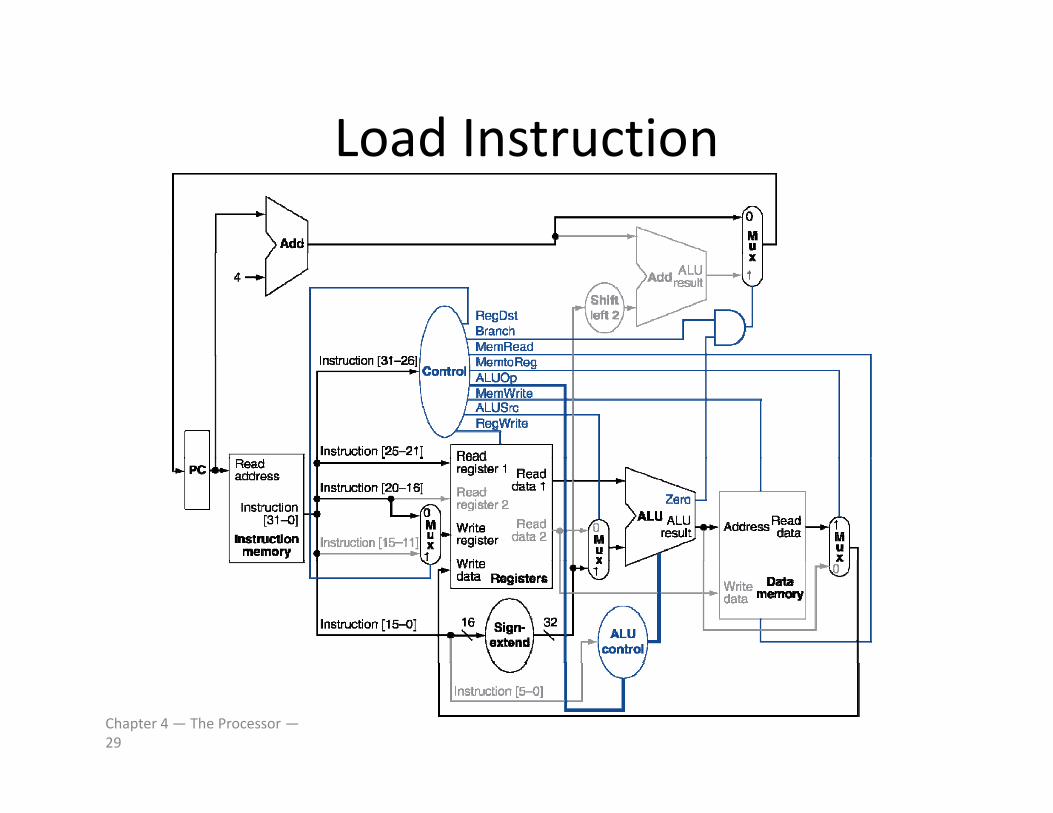
Load InstructionLoad Instruction
Chapter 4 — The Processor —29
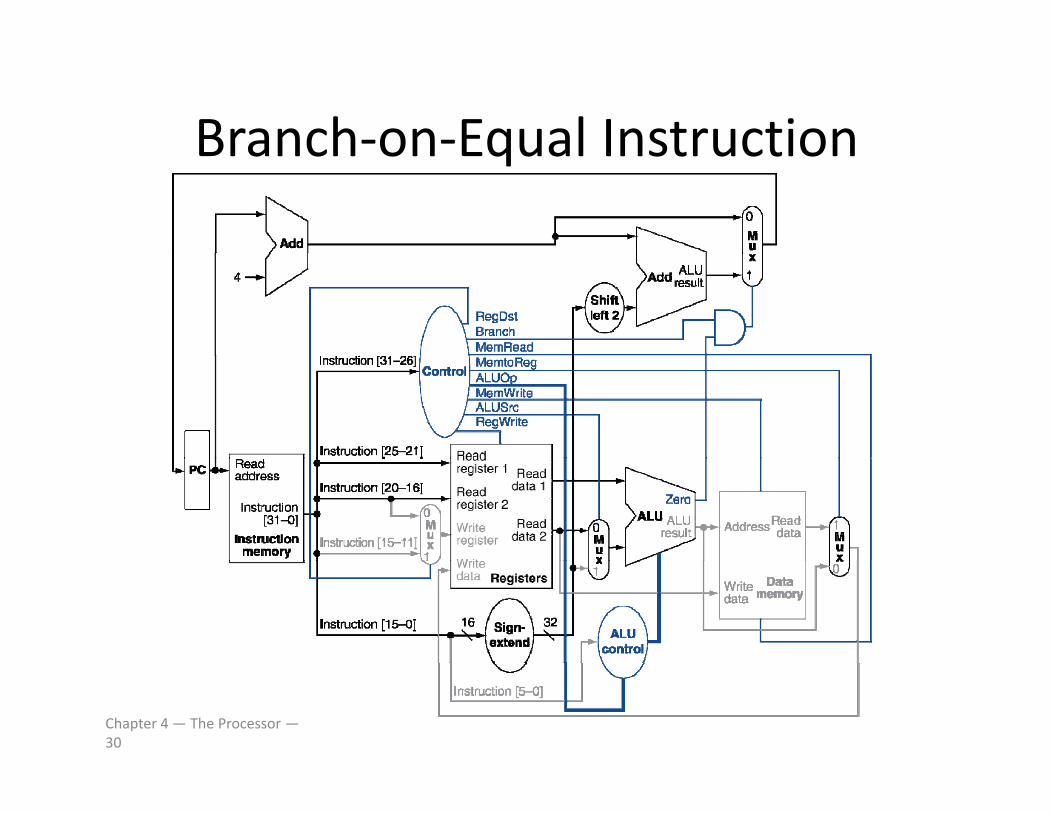
Branch‐on‐Equal InstructionBranch on Equal Instruction
Chapter 4 — The Processor —30
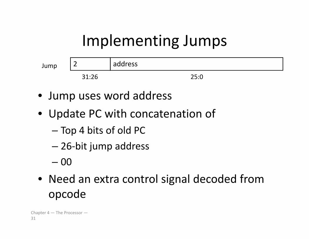
Implementing JumpsImplementing Jumps2 addressJump
• Jump uses word address
31:26 25:0
• Update PC with concatenation of– Top 4 bits of old PCp
– 26‐bit jump address
– 0000
• Need an extra control signal decoded from opcode
Chapter 4 — The Processor —31
opcode
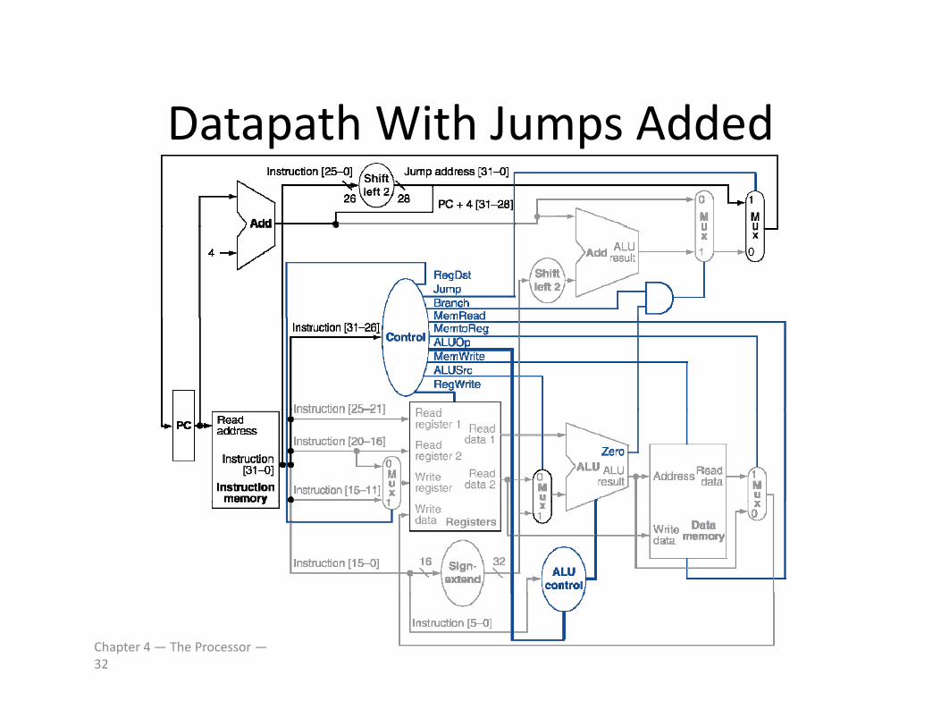
Datapath With Jumps AddedDatapath With Jumps Added
Chapter 4 — The Processor —32
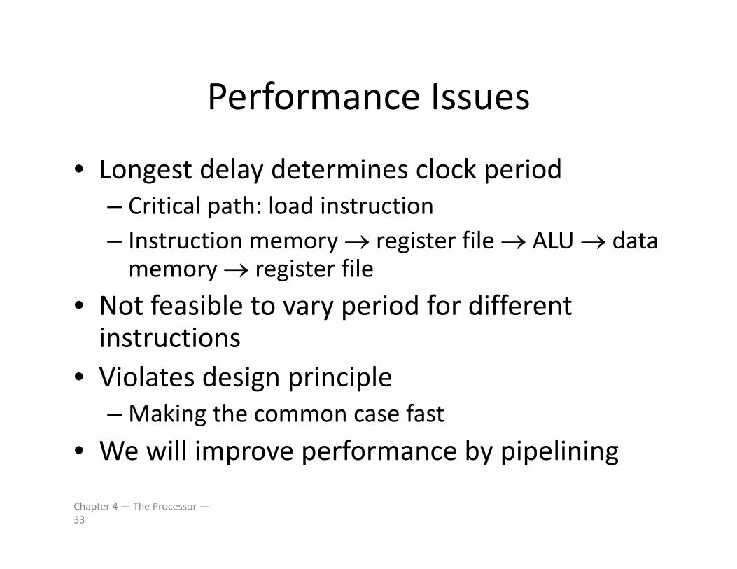
Performance IssuesPerformance Issues
• Longest delay determines clock periodLongest delay determines clock period– Critical path: load instruction– Instruction memory register file ALU data y g memory register file
• Not feasible to vary period for different instructions
• Violates design principle– Making the common case fast
• We will improve performance by pipelining
Chapter 4 — The Processor —33
p p y p p g
Example of more complex datapathExample of more complex datapathfrom BP
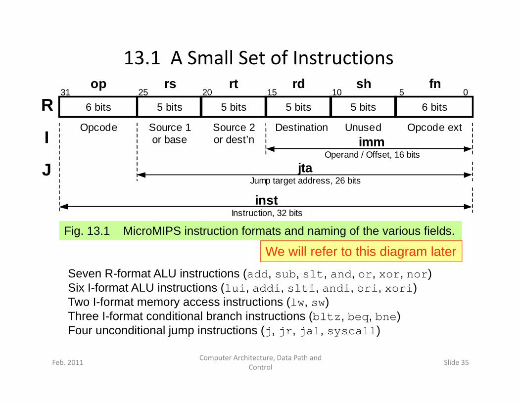
13.1 A Small Set of Instructions
5 bits 5 bits 31 25 20 15 0
O d S 1 S 2
op rs rt
R 6 bits 5 bits
rd
5 bits
sh
6 bits 10 5
fn
D ti ti U d O d tOpcode Source 1or base
Source 2or dest’n
jta
imm Operand / Offset, 16 bits
Destination Unused Opcode extI
J
Fi 13 1 Mi MIPS i i f d i f h i fi ld
Jump target address, 26 bits
inst Instruction, 32 bits
Fig. 13.1 MicroMIPS instruction formats and naming of the various fields.
Seven R-format ALU instructions (add, sub, slt, and, or, xor, nor)
We will refer to this diagram laterSeven R format ALU instructions (add, sub, slt, and, or, xor, nor)Six I-format ALU instructions (lui, addi, slti, andi, ori, xori)Two I-format memory access instructions (lw, sw)Three I-format conditional branch instructions (bltz, beq, bne)F diti l j i t ti (j j j l ll)
Feb. 2011Computer Architecture, Data Path and
ControlSlide 35
Four unconditional jump instructions (j, jr, jal, syscall)
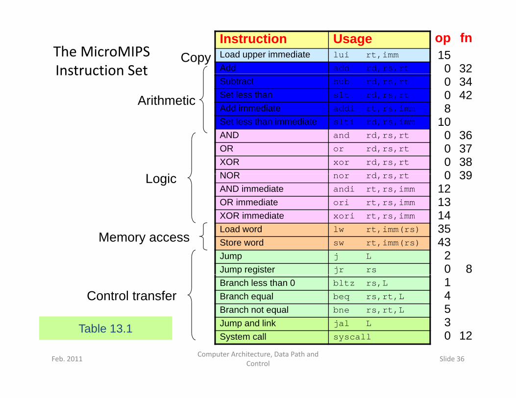
The MicroMIPS Instruction Set
Instruction UsageLoad upper immediate lui rt,imm
Add add rd,rs,rtCopy
op15
0
fn
32Instruction SetSubtract sub rd,rs,rt
Set less than slt rd,rs,rt
Add immediate addi rt,rs,imm
Set less than immediate slti rd,rs,imm
Arithmetic008
10
3442
Set less than immediate slti rd,rs,imm
AND and rd,rs,rt
OR or rd,rs,rt
XOR xor rd,rs,rt
NOR d tL i
100000
36373839NOR nor rd,rs,rt
AND immediate andi rt,rs,imm
OR immediate ori rt,rs,imm
XOR immediate xori rt,rs,imm
Logic 0121314
39
Load word lw rt,imm(rs)
Store word sw rt,imm(rs)
Jump j L
Jump register jr rs
Memory access3543
20 8
Branch less than 0 bltz rs,L
Branch equal beq rs,rt,L
Branch not equal bne rs,rt,L
Jump and link jal L
Control transfer1453T bl 13 1
Feb. 2011Computer Architecture, Data Path and
ControlSlide 36
Jump and link jal L
System call syscall
30 12Table 13.1
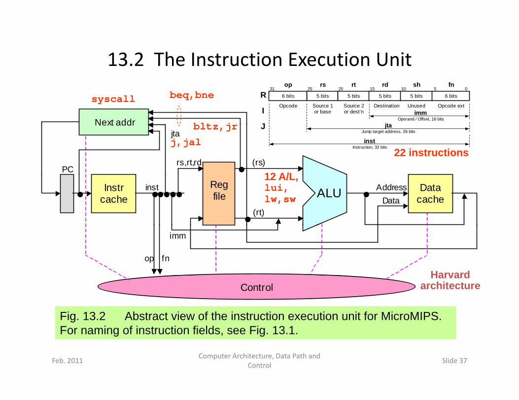
13.2 The Instruction Execution Unit
Next addr
5 bits 5 bits 31 25 20 15 0
Opcode Source 1 or base
Source 2 or dest’n
op rs rt
R 6 bits 5 bits
rd
5 bits
sh
6 bits 10 5
fn
jta
imm Operand / Offset, 16 bits
Destination Unused Opcode ext I
Jblt j
beq,bnesyscall
Next addr jta
rs,rt,rd (rs) PC
jtaJump target address, 26 bits Jinst
Instruction, 32 bits
bltz,jr
12 A/L
j,jal22 instructions
ALU
Data cache
Instr cache
Reg file
inst
(rt)
Address Data
12 A/L, lui, lw,sw
op fn
imm
Harvard
Fig. 13.2 Abstract view of the instruction execution unit for MicroMIPS. F i f i t ti fi ld Fi 13 1
Control Harvard
architecture
Feb. 2011Computer Architecture, Data Path and
ControlSlide 37
For naming of instruction fields, see Fig. 13.1.
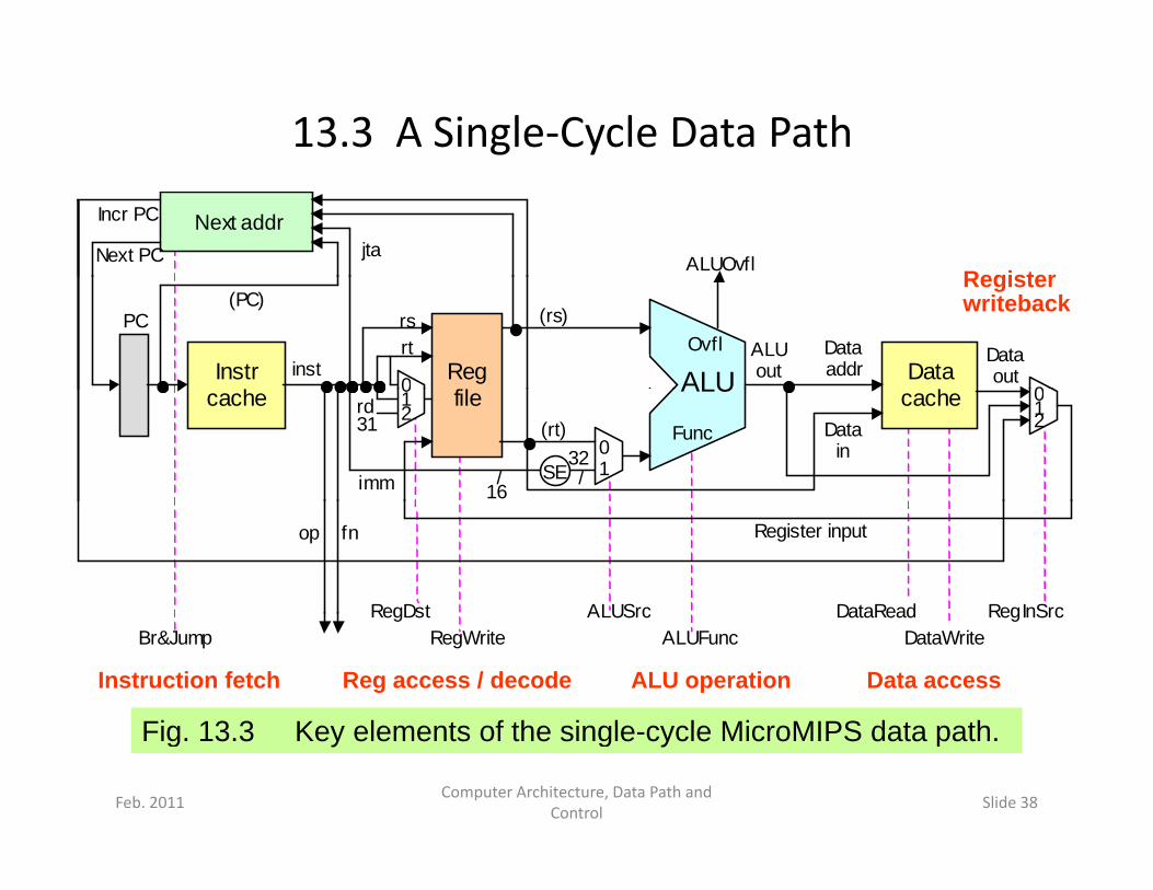
13.3 A Single‐Cycle Data Path
Next addr jta
ALUOvfl Next PC
Incr PC
Register
ALU Data Instr Reg f
inst
rs (rs) Data addr
rt Data out
Ovfl
0
(PC)
ALU out
PC
0
Register writeback
/
ALU cachecache file
imm
(rt) Data in 0
1 SE
rd
32 / 16
Func 31
012
01 2
op fn
ALUSrc DataRead RegInSrcRegDst
Register input
Fig 13 3 Ke elements of the single c cle MicroMIPS data path
ALUSrcALUFunc DataWrite
DataRead RegInSrcRegDstRegWrite Br&Jump
Instruction fetch Reg access / decode ALU operation Data access
Feb. 2011Computer Architecture, Data Path and
ControlSlide 38
Fig. 13.3 Key elements of the single-cycle MicroMIPS data path.
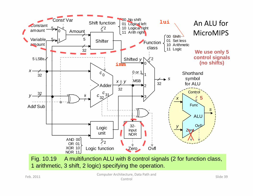
An ALU for MicroMIPSAmount
Constant amount 5
ConstVar
0
Shift function 2
00 Shift
00 No shift 01 Logical left 10 Logical right 11 Arith right
lui
Shifter 5 Variable amount
5 1 Function class
2 5 LSBs Shifted y
32
00 Shift01 Set less 10 Arithmetic 11 Logic We use only 5
control signals ( hift )
x y
x
Adder
c 0 s
0
1
2
y
32
32MSB
Shorthand symbol for ALU
0 or 1
imm (no shifts)
AddSub
y
Adder
c 32 k /
2
3 32 c 31
32
x
sFunc
Control 5
Logic unit
32-input NOR
ALU
y
s
Ovfl Zero
Fig 10 19 A multifunction ALU with 8 control signals (2 for function class
Logic function 2
NOR
Ovfl Zero
AND 00 OR 01
XOR 10 NOR 11
Feb. 2011Computer Architecture, Data Path and
ControlSlide 39
Fig. 10.19 A multifunction ALU with 8 control signals (2 for function class, 1 arithmetic, 3 shift, 2 logic) specifying the operation.
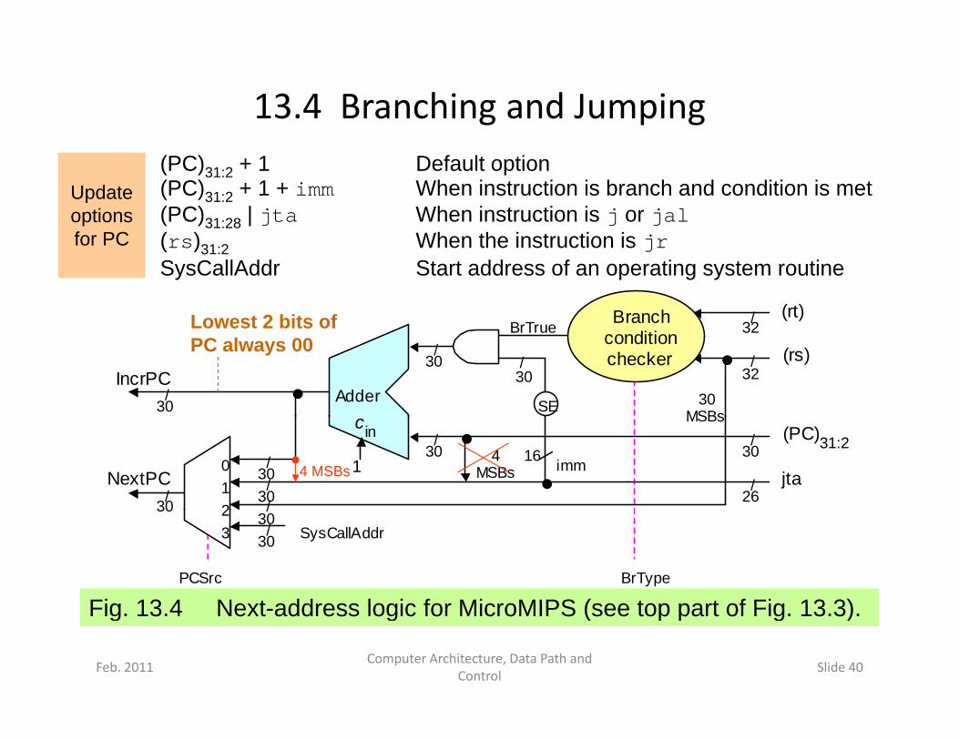
13.4 Branching and Jumping(PC)31:2 + 1 Default option(PC)31:2 + 1 + imm When instruction is branch and condition is met(PC)31:28 | jta When instruction is j or jal
Update options
(rt) Branch /32B T
(rs)31:2 When the instruction is jrSysCallAddr Start address of an operating system routine
for PC
Lowest 2 bits of
Adder
(rs)
SE
condition checker / 30
32BrTrue / 32
/ 30
30 MSBs
IncrPC / 30
Lowest 2 bits of PC always 00
jta imm
(PC) inc
1 0 1 2
/ 30 / / 30
/ 30
/ 30 / 26
/ 30 4 MSBs
MSBs
NextPC
31:2
16 4 MSBs
Fig 13 4 Ne t address logic for MicroMIPS (see top part of Fig 13 3)
SysCallAddr
PCSrc
2 3
30 / 30
/ 30
BrType
Feb. 2011Computer Architecture, Data Path and
ControlSlide 40
Fig. 13.4 Next-address logic for MicroMIPS (see top part of Fig. 13.3).
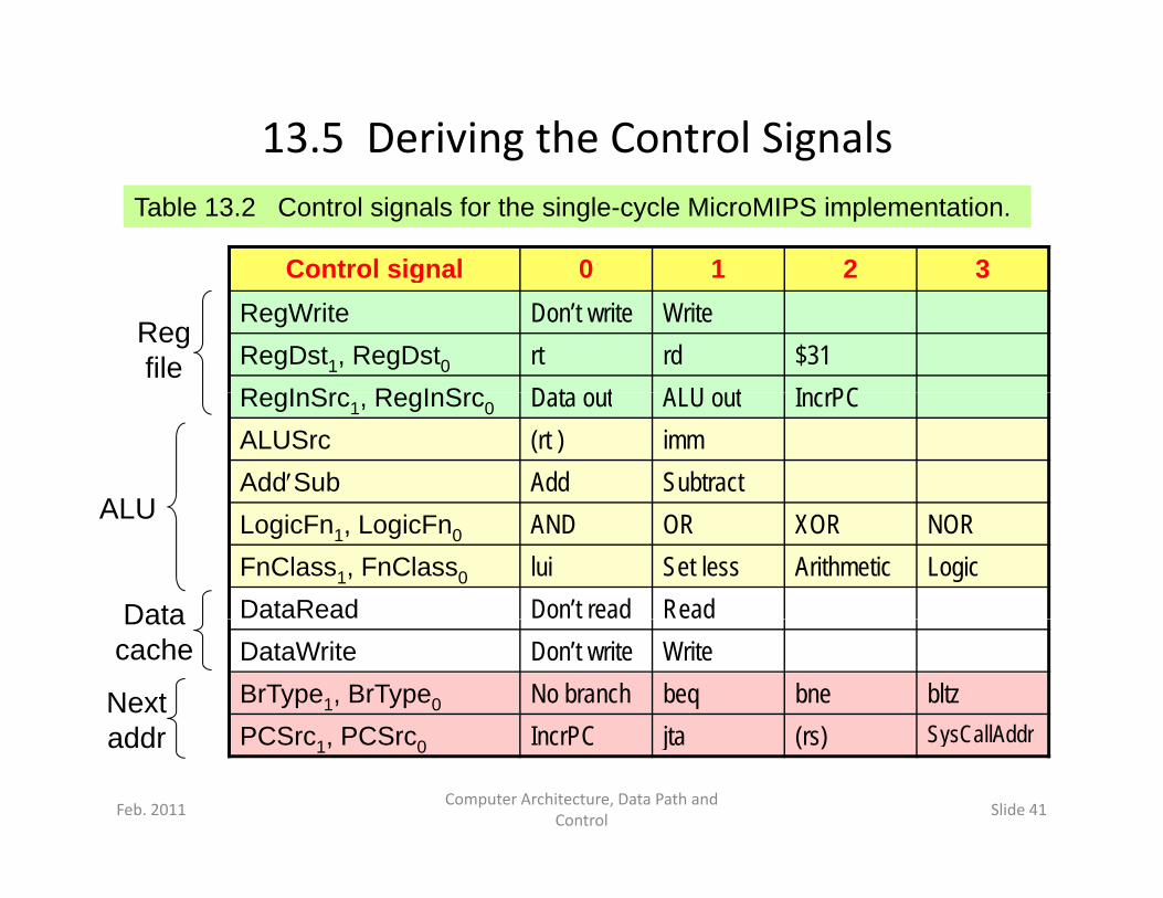
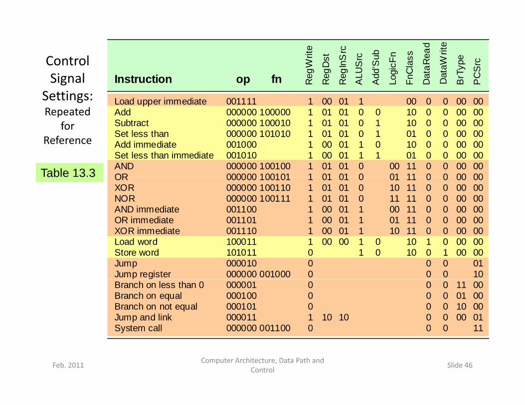
13.5 Deriving the Control SignalsTable 13.2 Control signals for the single-cycle MicroMIPS implementation.
Control signal 0 1 2 3gRegWrite Don’t write WriteRegDst1, RegDst0 rt rd $31RegInSrc RegInSrc Data o t ALU o t IncrPC
Reg file
RegInSrc1, RegInSrc0 Data out ALU out IncrPCALUSrc (rt ) immAddSub Add Subtract
ALU LogicFn1, LogicFn0 AND OR XOR NORFnClass1, FnClass0 lui Set less Arithmetic LogicDataRead Don’t read ReadData
ALU
DataWrite Don’t write WriteBrType1, BrType0 No branch beq bne bltzPCSrc PCSrc IncrPC jta (rs) SysCallAddr
Data cache
Next addr
Feb. 2011Computer Architecture, Data Path and
ControlSlide 41
PCSrc1, PCSrc0 IncrPC jta (rs) SysCallAddraddr
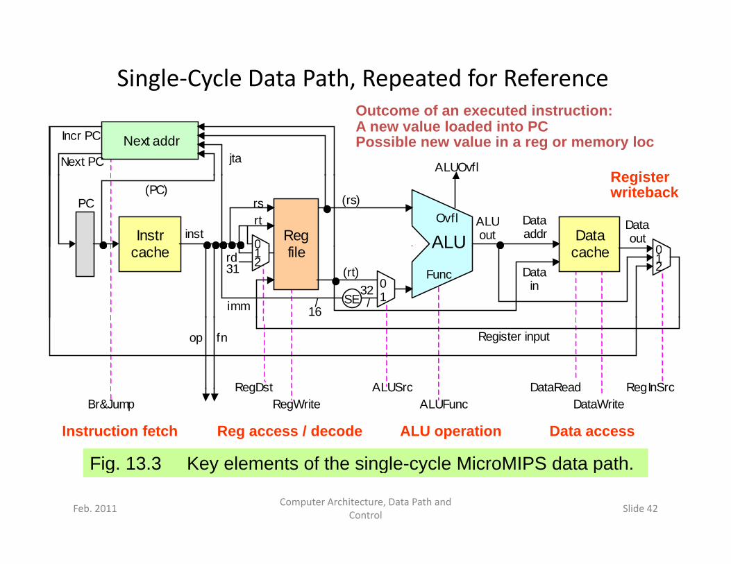
Single‐Cycle Data Path, Repeated for Reference
Next addr jta
ALUOvfl Next PC
Incr PC
Register
Outcome of an executed instruction:A new value loaded into PCPossible new value in a reg or memory loc
ALU Data Instr Reg f
inst
rs (rs) Data addr
rt Data out
Ovfl
0
(PC)
ALU out
PC
0
Register writeback
/
ALU cachecache file
imm
(rt) Data in 0
1 SE
rd
32 / 16
Func 31
012
01 2
op fn
ALUSrc DataRead RegInSrcRegDst
Register input
Fig 13 3 Ke elements of the single c cle MicroMIPS data path
ALUSrcALUFunc DataWrite
DataRead RegInSrcRegDstRegWrite Br&Jump
Instruction fetch Reg access / decode ALU operation Data access
Feb. 2011Computer Architecture, Data Path and
ControlSlide 42
Fig. 13.3 Key elements of the single-cycle MicroMIPS data path.
Control fI t ti eg
Writ
e
egD
st
egIn
Src
LUS
rc
dd’S
ub
gicF
n
nCla
ss
ataR
ead
ataW
rite
Type
CS
rc
Signal Settings Load upper immediate
Add Subtract
001111 000000 100000 000000 100010
1 1 1
op fn
00 01 01
01 01 01
1 0 0
0 1
00 10 10
0 0 0
0 0 0
00 00 00
00 00 00
Instruction Re
Re
Re
AL
Ad
Lo Fn Da Da
Br
PC
Table 13.3Subtract Set less than Add immediate Set less than immediate AND OR
000000 100010000000 101010 001000 001010 000000 100100 000000 100101
1 1 1 1 1 1
0101 00 00 01 01
0101 01 01 01 01
00 1 1 0 0
11 0 1
00 01
1001 10 01 11 11
00 0 0 0 0
00 0 0 0 0
0000 00 00 00 00
0000 00 00 00 00OR
XOR NOR AND immediate OR immediate XOR i di t
000000 100101000000 100110 000000 100111 001100 001101 001110
1 1 1 1 1 1
0101 01 00 00 00
0101 01 01 01 01
00 0 1 1 1
0110 11 00 01 10
1111 11 11 11 11
00 0 0 0 0
00 0 0 0 0
0000 00 00 00 00
0000 00 00 00 00XOR immediate
Load word Store word Jump Jump register
001110100011 101011 000010 000000 001000
1 1 0 0 0
0000
0100
11 1
0 0
10
1110 10
01 0 0 0
00 1 0 0
0000 00
0000 00 01 10
Branch on less than 0 Branch on equal Branch on not equal Jump and link System call
000001 000100 000101 000011 000000 001100
0 0 0 1 0
10
10
0 0 0 0 0
0 0 0 0 0
11 0110 00
00 00 00 01 11
Feb. 2011Computer Architecture, Data Path and
ControlSlide 43
System call 000000 001100 0
0 0 11
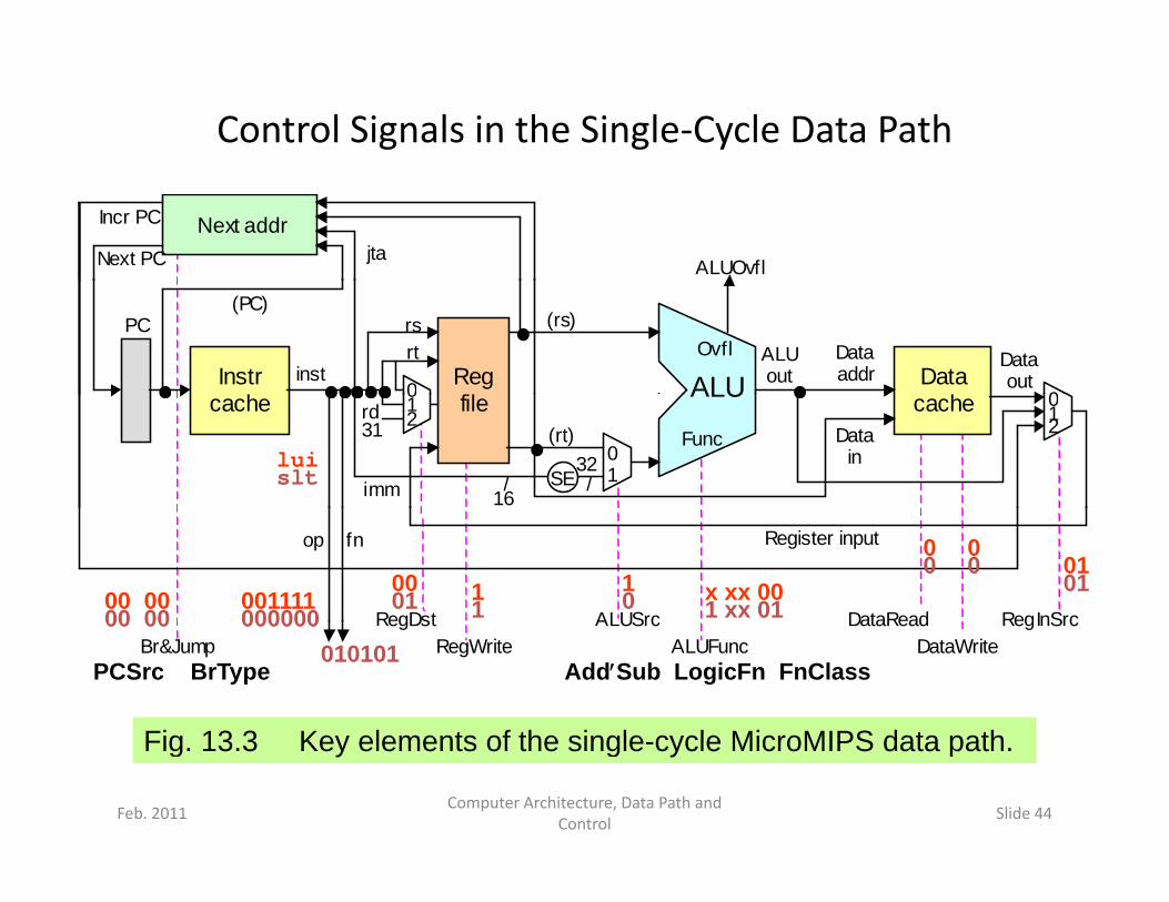
Control Signals in the Single‐Cycle Data Path
Next addr jta
ALUOvfl Next PC
Incr PC
ALU Data Instr Reg f
inst
rs (rs) Data addr
rt Data out
Ovfl
0
(PC)
ALU out
PC
0
/
ALU cachecache file
imm
(rt) Data in 0
1 SE
rd
32 / 16
Func 31
012
01 2
luislt
op fn
ALUSrc DataRead RegInSrcRegDst
Register input
001111 10001
1 x xx 00
0 0
00 00000000 101
010 1 xx 01
0 0
00 00
Fig 13 3 Ke elements of the single c cle MicroMIPS data path
ALUSrcALUFunc DataWrite
DataRead RegInSrcRegDstRegWrite Br&Jump
AddSub LogicFn FnClassPCSrc BrType
00000000 00010101
Feb. 2011Computer Architecture, Data Path and
ControlSlide 44
Fig. 13.3 Key elements of the single-cycle MicroMIPS data path.
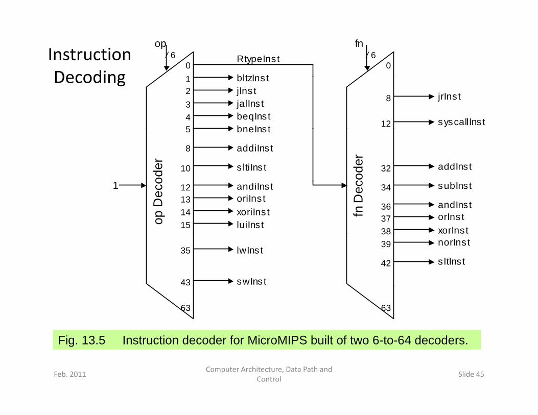
Instruction Decoding
RtypeInst
bltzInst0 1
/ 6 / 6 op fn
0 Decoding
jrIns t
syscallIns t
bltzInstjIns t jalIns t beqInst bneInst
12 3 4 5
8
12
addInst
bneInst
s ltiIns t
addiInst
1
5
10
8 od
er
code
r
32
orInst xorInst
andInst
subInstandiInstoriIns t xoriIns t luiIns t
1 12 13 14 15 op
Dec
o
fn D
ec 34
36 37 38
norInst
s ltIns t lwInst
swInst
35
43
3839
42
Fig 13 5 Instruction decoder for MicroMIPS built of two 6 to 64 decoders
63 63
Feb. 2011Computer Architecture, Data Path and
ControlSlide 45
Fig. 13.5 Instruction decoder for MicroMIPS built of two 6-to-64 decoders.
Control Si l fI t ti eg
Writ
e
egD
st
egIn
Src
LUS
rc
dd’S
ub
gicF
n
nCla
ss
ataR
ead
ataW
rite
Type
CS
rc
Signal Settings:Repeated
for
Load upper immediate Add Subtract
001111 000000 100000 000000 100010
1 1 1
op fn
00 01 01
01 01 01
1 0 0
0 1
00 10 10
0 0 0
0 0 0
00 00 00
00 00 00
Instruction Re
Re
Re
AL
Ad
Lo Fn Da Da
Br
PC
for Reference
Table 13.3
Subtract Set less than Add immediate Set less than immediate AND OR
000000 100010000000 101010 001000 001010 000000 100100 000000 100101
1 1 1 1 1 1
0101 00 00 01 01
0101 01 01 01 01
00 1 1 0 0
11 0 1
00 01
1001 10 01 11 11
00 0 0 0 0
00 0 0 0 0
0000 00 00 00 00
0000 00 00 00 00ab e 3 3 OR
XOR NOR AND immediate OR immediate XOR i di t
000000 100101000000 100110 000000 100111 001100 001101 001110
1 1 1 1 1 1
0101 01 00 00 00
0101 01 01 01 01
00 0 1 1 1
0110 11 00 01 10
1111 11 11 11 11
00 0 0 0 0
00 0 0 0 0
0000 00 00 00 00
0000 00 00 00 00XOR immediate
Load word Store word Jump Jump register
001110100011 101011 000010 000000 001000
1 1 0 0 0
0000
0100
11 1
0 0
10
1110 10
01 0 0 0
00 1 0 0
0000 00
0000 00 01 10
Branch on less than 0 Branch on equal Branch on not equal Jump and link System call
000001 000100 000101 000011 000000 001100
0 0 0 1 0
10
10
0 0 0 0 0
0 0 0 0 0
11 0110 00
00 00 00 01 11
Feb. 2011Computer Architecture, Data Path and
ControlSlide 46
System call 000000 001100 0
0 0 11
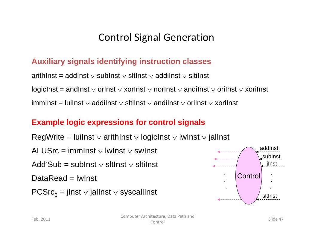
Control Signal Generation
Auxiliary signals identifying instruction classes
arithInst = addInst subInst sltInst addiInst sltiInstarithInst = addInst subInst sltInst addiInst sltiInst
logicInst = andInst orInst xorInst norInst andiInst oriInst xoriInst
immInst = luiInst addiInst sltiInst andiInst oriInst xoriInst
Example logic expressions for control signals
RegWrite = luiInst arithInst logicInst lwInst jalInstRegWrite = luiInst arithInst logicInst lwInst jalInst
ALUSrc = immInst lwInst swInst
AddSub = subInst sltInst sltiInst
addInstsubInst
jInst
DataRead = lwInst
PCSrc0 = jInst jalInst syscallInst
Control
sltInst
.
..
.
..
Feb. 2011Computer Architecture, Data Path and
ControlSlide 47
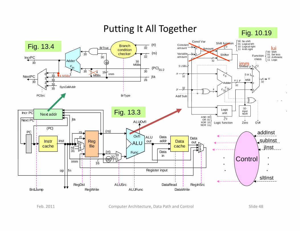
Putting It All Together Fig. 10.19ConstVar Shift f ti
00 No shif t
Shifter
Amount
5
Constant amount
Variable amount
5
5
0
1
0
Function class
2
Shift function
5 LSBs Shifted y
32
2
00 Shif t 01 Set less 10 Arithmetic 11 Logic
01 Logical lef t10 Logical right 11 Arith right
imm
lui
Adder
(rs)
(rt)
SE
(PC)
Branch condition checker
in c
/ 30
/ 32 BrTrue / 32
/ 30
/ 30
/ 30 4
30 MSBs
IncrPC / 30
31:2 16
Fig. 13.4
AddSub
x y
y
x
Adder
c 32
c 0
k /
s 1
2
3
32
32 c 31
32 32
MSB
x
Shorthsymbfor AL
Fun
Cont
0 or 1 jta
imm
SysCallAddr
PCSrc
1 0 1 2 3
/ 30 / 30
/ 30
/ 30
/ 30 30
/ 26
30 4 MSBs
BrType
NextPC 16
4 MSBs
Next addr jta
( )
ALUOvfl Next PC
Incr PC
(PC)
Fig. 13.3 Logic unit
Logic function 2
32-input NOR
Ovfl Zero
A
y OZero
AND 00 OR 01
XOR 10 NOR 11
/
ALU
Data cache
Instr cache
Reg file
inst
rs (rs)
(rt)
Data addr
Data in 0
1SE
rt
rd
32 /
Data out
Func
Ovfl
31
0 1 2
( )
ALU out
PC
0 1 2
Control
addInstsubInst
jInst
../
op fn
imm 1
ALUSrc ALUF D t W it
DataRead
SE
RegInSrcRegDst R W it
/16
Register input
B &J
Control
sltInst
..
..
Feb. 2011 Computer Architecture, Data Path and Control Slide 48
ALUFunc DataWriteRegWriteBr&Jump
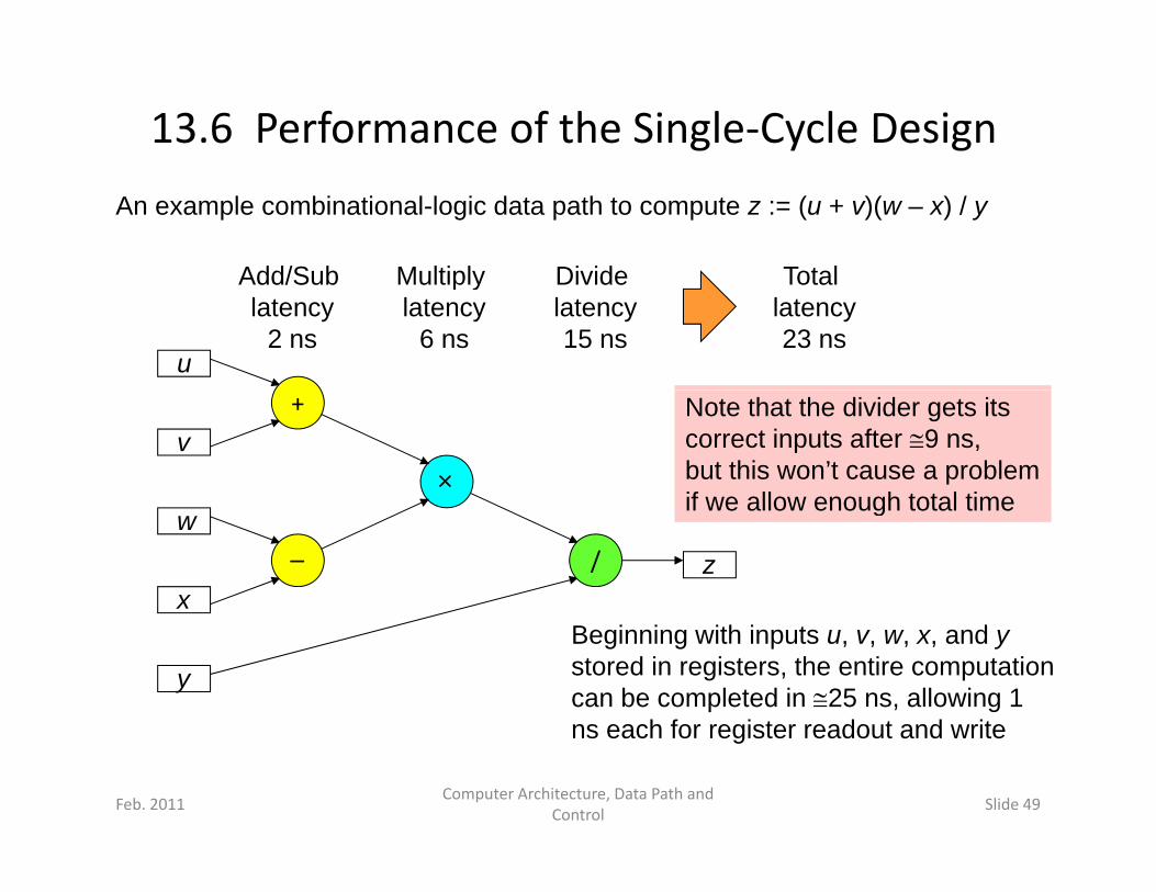
13.6 Performance of the Single‐Cycle Design
An example combinational-logic data path to compute z := (u + v)(w – x) / y
Add/Sub Multiply Divide TotalAdd/Sub latency
2 ns
Multiply latency
6 ns
Divide latency15 ns
Total latency23 ns
u
Note that the divider gets its correct inputs after 9 ns, but this won’t cause a problem if we allow enough total time
+
v
if we allow enough total time
/w
xz
Beginning with inputs u, v, w, x, and y stored in registers, the entire computation can be completed in 25 ns, allowing 1 ns each for register readout and write
y
Feb. 2011Computer Architecture, Data Path and
ControlSlide 49
ns each for register readout and write
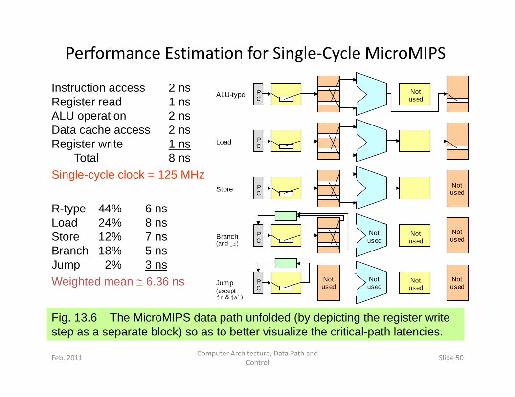
Performance Estimation for Single‐Cycle MicroMIPS
Instruction access 2 nsRegister read 1 nsALU operation 2 ns
P C
ALU-type Not used
Data cache access 2 nsRegister write 1 ns
Total 8 nsSingle cycle clock = 125 MHz
P C
Load
Single-cycle clock = 125 MHz
P C
Store Not used
R-type 44% 6 nsLoad 24% 8 ns
P C
Branch Not used
Not used
Not used (and jr)
Load 24% 8 nsStore 12% 7 nsBranch 18% 5 nsJump 2% 3 ns
Fig. 13.6 The MicroMIPS data path unfolded (by depicting the register write
P C
Jump Not used
Not used
Not used
Not used (except
jr & jal)
Weighted mean 6.36 ns
Feb. 2011Computer Architecture, Data Path and
ControlSlide 50
g p ( y p g gstep as a separate block) so as to better visualize the critical-path latencies.
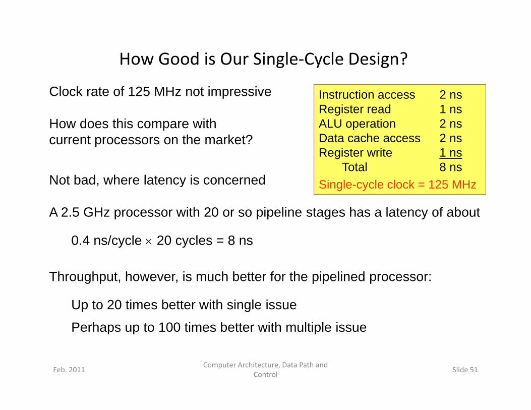
How Good is Our Single‐Cycle Design?
Instruction access 2 nsRegister read 1 nsALU operation 2 ns
Clock rate of 125 MHz not impressive
How does this compare with ALU operation 2 nsData cache access 2 nsRegister write 1 ns
Total 8 ns
How does this compare with current processors on the market?
Not bad where latency is concerned Single-cycle clock = 125 MHzNot bad, where latency is concerned
A 2.5 GHz processor with 20 or so pipeline stages has a latency of about
0.4 ns/cycle 20 cycles = 8 ns
Throughput, however, is much better for the pipelined processor:g p , , p p p
Up to 20 times better with single issue
Perhaps up to 100 times better with multiple issue
Feb. 2011Computer Architecture, Data Path and
ControlSlide 51
p p p
Related Documents