UNCLASSIFIED AD 2 6 8 169 ARMED SERVICES TECHNICAL INFORMATION AGENCY ARLINGTON HALL SFATKON ARLINGTON 12, VIRGINIA UNCLASSIFIED

Welcome message from author
This document is posted to help you gain knowledge. Please leave a comment to let me know what you think about it! Share it to your friends and learn new things together.
Transcript
UNCLASSIFIED
AD268 169
ARMED SERVICES TECHNICAL INFORMATION AGENCYARLINGTON HALL SFATKONARLINGTON 12, VIRGINIA
UNCLASSIFIED
NOTIC: 'en government or other drawings. spool-fications or other data are used for any purposeother than in connction vith a definitely relatedgoverment procur nt operation. the U. S.Government thereby incurs no responaibility, nor anyobliS~tion 4hatsoever; and the fact that the Govern-ment may have forualated, furnished, or in any waysupplied the said drawings, specifications, or otherdata i not to be reprded by implication or other-vise as in any smner licensing the holder or anyother person or corporation, or conveying any rittsor permission to mnufacture, use or sell anypatented invention that my in my vay be relatedthereto.
14YJ 1. t
?II
MC lI::z : .
IID
III
I
PRODUCTION ENGINEERING MEASUREON
300 WATT SILICON AUDIO TRANSISTOR
Contract No. DA-36-o39-SC-85968
for
Production Development DivisionDivision for Industrial Mobilization
The Army Signal Supply AgencyPhiladelphia, Pennsylvania
PERIOD COVERED:
21 June, 1961 - 30 September, 1961
I
Written By: Reviewed By: , .pr ed rA
S. Silverstein H. Meisel K.E. Loofbour w,, ManagerIndustrial TraMsistorProduct Development
Edited By:
L T. McCH. Id s l er
RADIO CORPORATION OF AMERICA
Materials and Semiconductor Division Somerville, New Jersey
I
I DISTRIBUTION LIS
DESTINATION COPIES
Commanding Officer 3SU.S. Army Signal Research and Development LaboratoryFort Monmouth, New JerseyATTN: Dr. Harold Jacobs
Solid State and Frequency Control Division
Commander 2Wright Air Development DivisionWright Patterson Air Force Base, OhioATTN: Mr. R. D. Alberts, WCLKS
Advisory Group on Electronic Devices 2346 Broadway, 8th. FloorNew York 13, N. Y.
Director 1Armed Services Electro-Standards AgencyFort Monmouth, New JerseyATTN: Adjutant
Armed Services Technical Information Agency 10Arlington Hall StationArlington 12, VirginiaATTN: TICSCA/42740
Commander 1Air Research and Development CommandAndrews Air Force BaseWashington 25, D. C.ATTN: RDTCT
Air Force Cambridge Research CenterL. G. Hanscom FieldBedford, MassachusettsATTN: Mr.. R. A. Bradbury CRRSC
A. H. Young 1Dept. of the NavyBureau of ShipsSemiconductors Group, Code 691 AlWashington 25, D. C.
G. Abraham, Code 5266U. S. Naval Research LaboratoryWashington 25, D. C.
- ii-
DISTRIBUTION LIST (CONT.)
DESTINATION COPIES
Canadian Liaison OfficeOffice of the Chief Signal OfficerDepartment of the ArmyThe PentagonWashington 25, D. C.ATTN: SIGEO-CL
Sylvania Electric Products, Inc.100 Sylvan RoadWoburn, MassachusettsATTN: Library
Texas Instruments, Inc.Semi-conductor-Components DivisionP. 0. Box 312Dallas 21, TexasATTN: Semi-conductor Library
Transitron Electronic Corporation 1168-182 Albion StreetWakefield, MassachusettsATNT: Dr. D. Bakalar
Commanding Officer
U. S. Army Signal Material Support AgencyFort Monmouth, New JerseyATTN: Mr. Leon Kramer
Chief Signal OfficerDepartment of the ArmyMain Navy Building
Washington 25, D. C.ATTN: Mr. Charles Holman
Chief, P and D Division(SIGPD-5b-1)
Western Electric fmpany 2Marian and Vine StreetsLaureldale, Penna.ATTN: Mr. Robert Moore
Westinghouse Electric CorporationYoungwood, Pennsylvania
Diamond Ordance Fuze LaboratoriesConnecticut and Van Ness Streets, N. W.Washington 25, D. C.ATTN: DOFL Library
Room 211Building 92(oRDTL-oll-59-138L)
-iii-
DISTRIBUTION LIST (CONT.)
DESTINATION COPIES
Clevite-Transistor Products, Inc. 1241-57 Crescent StreetWaltham 54, Massachusetts
General Electric CompanyElectronic ParkSyracuse, N. Y.ATTN: Mr. J. Flood
Hughes ProductsSemi-conductor DivisionNewport Beach, California
Minneapolis-Honeywell Regulator Company2753 Fourth Avenue SouthMinneapolis 8, Minnesota ,ATT14- Mr. D. R. Paler
Mororola, Inc.5005 East McDowell RoadPhoenix, ArizonaATTN: Mr. James S. LaRue
Pacific Semi-conductors, Inc.10451 West Jefferson BoulevardCulver City, CaliforniaATTN: Dr. H. Q. North
Lansdale Tube CompanyChurch RoadLansdale, PennsylvaniaATTN: Mr. Frank Mayock
Mgr - Gov't Sales
* - Raytheon Manufacturing Company150 California StreetNewton, MassachusettsATTN: Mr. Frank Dukat
Comanding OfficerWestern Regional Office
" 125 South Grand AvenuePasadena 2, CaliforniaATTN: Mr. Gershon Miller
International Rectifier Corporation1521 East Grand AvenueEl Segundo, CaliforniaATTN: Mr. Angus Scott
- iv-
DISTRIBUTION LIST (CONT.)
DESTINATION COPIES
Ordnance Corps 1
Picatinny ArsenalDover, New Jersey
-ATTN: Mr. Christ C. Anagnost
Dr. Robert H. Rediker, Gr 85 1
Division 8, Room C-310Linclon LaboratoryLexington, Massachusetts
Silicon Transistor Corporation 1
Carle PlaceLong Island, N. Y.
U. S. Army Signal Supply Agency 6225 So. 18th. StreetPhiladelphia 3, PennsylvaniaATTN: SIGSU-R2
1.
111

Iv -
TABLE OF CONTENTS
I Page
I. PURPOSE . . . . . . . . . . . . . . . . . . . . . . . . . . . . . . . 1
II. DEVICE DESIGN CONSIDERATIONS .... ..................... 2
A. General ........................ ....... .. . ....... 2
I B. Collector Breakdown Voltage............................ ... 2
C.* Current Gain . . . . .. .. . . ... . . . . . * . . ... . * 3
D. Thermal Resistance . ........ * . . . ........... 4
I E. Power Gain .......... .. . .. .. * . . .* . . . . . .. . 5
F. Case Design ................... ....... 7
I G. Power Dissipation .......... .. ........................ 7
III. DEVICE FABRICATION .......... . ............. 11
A. Parts and Materials ...................... .1
B. Processes and Processing. ................... 1. i
1. General....................... ..
.. 2. Diffusion . . . . . . . . . . . . . . . . . . . . .. ii
3. Collector Formation . .. . .......... .... 15
4o Base Formation o.. . .... ..... 15
5. Emitter Formation. ........... . . . o . . . . . . . . 15
6. Contacting . o. . .. . . . . . . . . ... . . . . 15V
7. Mesa Formation . . . . ................ . . 15
S8. Dicing . .. .. . . o.. .. . . ... .. .. . 15
9. Mounting and Sealing ... .. ................ . 1
IV. DEVICE EVALUATION. .. ................ . . . o . o . . . . . 19
A. Electrical ........ .......................... . . 19
B. Environmental . ............................... . 19
-vi-'I TABLE OF CONTENTS CONT.
V.CNLSOSj Page
V.~~~~ CCLSOS. .. . ............. ............ 20
1VI. PROGRAM FOR NEXDT QUARTER . . . . .. .. .. . .. .. .. .. .. .21
VII. PERSONNEL AND MAN HOURS .. .. .. .. .. ..... ........ . . 22
i-vii-
I LIST OF FIGURES
Figure Number Title Page
1 Derating Curve for Type TA 2167 ...... .............. 6
j 2 Double-Ended Stud Package for the TA 2167......... 8
3 Photograph of Single-Ended Stud Packages Used to EncloseI Initial State-of-the-Art Samples ...... . . . * . . 9
4 Parts and Materials Flow Chart for TA-2167 Type Transistor 12
j 5 A Flow Chart of Present Processing for the TA-2167 SiliconPower Transistor ..................... . 13
6 Impurity Profile for High Voltage Silicon Transistors. . . 14
7 Photograph of a Device Showing the 0.050" Molybdenum Plat-form Located on the Header After the Leads have.Beei Removed17
8 Photograph of a Unit Bonded Using the Two Gold Ribbons . . 18
LIST OF TABLES
Table Number Title Page
I Electrical Characteristics of Initial Five State-of-the-Art Samples. . . . . . . . ... . . . .. .. . . . 19
II Man Hours for First Quarter. . . . . .. .. .. . ... 25
-viii-
LIST OF SYMBOLS
Symbol Explanation
BVc 0 Breakdown Voltage, Collector-to-Base, emitter open
BVEBO Breakdown Voltage, Emitter-to-Base, collector open
Cob Output Capacitance, common base
f Maximum Frequency of Oscillationmax
I Intrinsic or undiffused layer
IC Collector current, DC
ICBO Collector Cutoff Current, DC, emitter open
I CER Collector Cutoff Current, DC, with specified resistance betweenbase and emitter
IEBO Emitter Cutoff Current, DC, collector open
rbb, Base Spreading Resistance
RBE External Base-to-Emitter Resistance
lec Maximum Allowable Transit Time, Minority Carrier, Emitter-to-Collector
-e Emitter Phase Delay Time
ITb Base Transit Time
-1 Collector Transit Time
VCBO Collector-to-Base Voltage, DC, emitter open
V CEO Collector-to-Emitter Voltage, DC, base open
VCER Collector-to-Emitter Voltage, DC, with specified resistancebetween emitter and base
kt Constant equal to 0.026 voltsq
h FE Static value of the forward current transfer ratio (common emitter)
VCE (sat) Collector-to-Emitter Saturation Voltage
n Efficiency
Q Thermal ResistanceII

-ix-
ABSTRACT
This abstract gives a brief description of the significant accomplishments
of Signal Corps Three-Hundred Watt Audio Transistor Program DA-36-039-SC-85968
by the Radio Corporation of America (Semiconductor and Materials Division) dur-
ing the period from June 21, 1961 to September 30, 1961.
A triple-diffused, NPIN transistor has been selected as the device for fab-
rication as the specified three-hundred watt, audio transistor. This type of
structure will permit the desired characteristics of reduced base resistance,
minimized collector-to-emitter punch-through voltage, high collector breakdown
voltages, small base widths without reaching a punch-through condition, and good
current gains. Calculations have been made of the collector breakdown voltage,
current gain, thermal resistance, power gain, and power dissipation, and with
a few reservations, the present device geometry should satisfy the contract
specifications. A new case, a double-ended stud package, has been designed, and
parts ordered.
The tentative Process Flow Chart for the device fabrication is as follows:
Wafer Preparation; Multiple Collector Formation; Multiple EmitterFormation; Multiple Contacting; Multiple Mesa Formation; PelletSeparation; Individual Device Mounting and Sealing; and Individual
Device Evaluation.
In the mounting and sealing area, some work has been done to use a molybdenum
platform, 0.050" thick, between the pellet and the header. This particular thick-
ness prevents problems with warping in subsequent fabrication processes. A change
in the type of material used to contact the mesa has been made. Gold ribbon is
now used in place of the previously used gold wire because of the increased cur-
rent-handling capabilities possible.
Five state-of-the-art samples of the device have already been given to Mr.
C. Fisher of the Signal Corps on September 22, 1961, and the electrical characteristics
are presented.
rThe biographies of the personnel contributing directly to this program are
presented and the Man Hours for this quarter and to-date are included.
-1-
I. PURPOSE
The purpose of this contract is to establish an industrial capability to
manufacture a 300 watt silicon transistor. This capability will be demonstrat-
ed by operating a pilot line, containing the necessary prototype (where applica-
ble) equipment to fabricate this device, capable of a production rate of at
least 200 transistors, conforming to the applicable specifications (MIL-S-19500B,
SCS-100 etc.), per eight (8) hour 'hift day. Furthermore, a total of 175 samples
must be submitted to the Contracting Agency, together with all required reports.
In addition, 1000 transistors from the pilot line conforming to the applicable
specifications will be submitted.
11
I
-2-
II. DEVICE DESIGN CONSIDERATIONS
A. General
The design selected as the one for the TA-2167 (subject contract de-
vice) is a triple-diffused, NPIN structure. An NPIN transistor differs
from a conventional NPN transistor in that it has a high resistivity layer
.- in the collector body. In an NPN structure, the collector-to-base break-
down voltage is dependent primarily upon the impurity gradient in the base
and the background resistivity of the collector. A shallow impurity gradient
in the base is therefore necessary to obtain a high collector-to-base
breakdown voltage. In an intrinsic layer device, the collector breakdown
voltage is dependent primarily on the width of the intrinsic layer. The
depletion region will extend primarily into the collector body thereby reduc-
ing the field strength at a given reverse voltage. Therefore, a highly doped
jbase region can be used in an NPIN device to reduce base resistance and
minimize collector-to-emitter punch-through voltage while simultaneously
permitting high collector breakdown voltages. The base widths can be made
extremely small without reaching a punch-through condition, and good current
gains can be achieved.
j The first consideration in the design of this device is to obtain the
required 300 volt collector-breakdown voltage both in the open-emitter and
open-base configurations.
B. Collector Breakdown Voltale
The theoretical breakdown field for 20-40 ohm-cm silicon is about 3xlO
1 volts/cm or 750 volts/mil. However, experience has shown that because of
variations in the intrinsic layer width (caused by uneven impurity penetra-
tions and lapping) a wider intrinsic layer than estimated by this figure should
3-
I be used. In practice, a 2.0 mil intrinsic layer will result in an 800
volt collector breakdown in the open-emitter circuit configuration.
The collector-to-emitter, open-base voltage (VCEO) can be estimated
1 from the following relationship:
VCBO
VE = fe + 1
For this device, the empirically derived a lanche multiplication factor(n)
has a value of 9. For units having a current gain of 50, and still meeting
I the 300 volt VCE0 requirement, a VCB0 of 550 volts is required. Therefore,
a 2 mil intrinsic layer will provide a transistor that will meet the con-
tract collector specification.
j C. Current Gain
At sufficiently high current levels all transistors show a fall-off of cur-
I rent gain with current. The specification for this device requires a cur-
I rent gain of 15-45 at a collector current of five amperes, and 10 at a col-
lector current of ten amperes.
Previous investigations conducted have shown that, at high current den-
sities, a transverse voltage develored in the base layer causes carrier in-
Ijection to be confined primarily to the edges of the emitter. Therefore, the
emitter peripheral distance, rather than the emitter area, is the significant
parameter in the design consideration. E'perience has shown that current
gain will peak at a current density of approximately one ma/mil of emitter
periphery. Originally, an emitter periphery of five inches was thought to
be necessary, but recent data indicate that 2.2 inches of emitter periphery
are adequate.
.. -4-
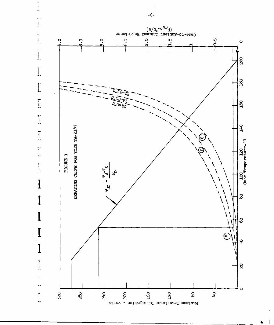
D. Thermal Resistance
The maximum junction to case thermal resistance of the TA-2167 is 0.38
OC/watt. This value is determined by the specified values of 300 watts pow-
Ier dissipation, 200 C maximum junction temperature, and 250C case temp-
erature and can be calculated according to the following equation:
in C . . . . . . . . ........ . . (2)
Assuming the transistor operates as an amplifier with 65% efficiency,
I the power to be dissipated by each transistor, when two units are operat-
ing in push-pull with a power output of 500 watts, can be determined from
Ithe following:
I D (Po) (5)
jThis dissipation, when calculated, is 135 watts for each of the transistors.
The maximum allowable case-to-ambient thermal resistance is 1.3 0C/watt when
Icalculated from the following equation:TJ - TASJA PD. (4)
PD
Since the junction-to-case thermal resistance is 0.58 °C/watt, the maximum
case-to-ambient thermal resistance is about 0.7 *C/watt. This low thermal
resistance requirement will mean that the unit should be operated in a water-
cooled heat sink when large amounts of power must be dissipated.
" - Some preliminary design work has been done in the area of Thermal
Rating of the TA-2167. Theoretically this device is capable of dissipat-
ing 300 watts if the transistor case can be maintained at the ambient temp-
erature of 250C. As the ambient temperature increases, the corresponding
-5-
maximum ti nsistor dissipation decreases. The rate of decrease in PD max
1 can be determined from the derating curve for the device. The negative
slope of this curve represents the thermal resistance of the transistor.
If the case temperature is to be maintained at the ambient temperature,
any operating point along the derating curve would require an infinite
I heat sink.
i In most silicon transistor applications the ambient temperature is
considerably lower than that of the case. This temperature difference
divided by the power dissipation determines the minimum case-to-ambient
thermal resistance required to keep the junction temperature within the
Tmaximum rating of 2000C.The case-to-ambient thermal resistance consists of the contact thermal
resistance and the heat sink thermal resistance. A plot of the case-to-
ambient thermal resistance (0C) versus TC for various ambient temperatures
°- is superimposed on the derating curve for the TA-2167 in Figure 1. This
" graph enables the designer to determine the minimum case-to-ambient thermal
resistance necessary to prevent overheating the junction. Further work
is continuing in this area.
E. Power Gain
The peak current of the TA-2167 can be calculated from the following
I equation: IEpP - _ _(5)
For an AC power of 250 watts per device operating at 120 volts, the peak
.I current is 8.3 amperes. The load resistance for the transistor at this
voltage and current level is then computed as follows:
E
- P (6)I p
-6-
aoms~a lsuq qXLJ ua~qurv-oq-a9voo0 I 0 AI0
1.-
I -l
0N 0
1. C.?
sqq-em ~ ~ ~ ~ ® \\O~dSTIaqss"j fn~v
7° -7-
and is equal to 14.4 ohms. The power gain can then be estimated from the
-" following equation:
.. P.G. . . . . . . . . . . . . . . . . ... (7)BIN
To obtain a minimum beta of ten and a power gain of twenty-five db, as
specified in the technical requirements, the maximum input resistance is 4.6
ohms. No difficulty is anticipated in meeting this specification because
the input resistance is expected to be about one ohm.
F. Case Design
A double-ended stud package has been designed for this device, and will
jbe used to dissipate the heat required. A drawing of this package is shown
in Figure 2. Sample parts have been received and are presently being evaluat-
ed. Delivery of reasonable quantities of this package for device fabrication
are not due until late in October. At that time, use of the new case design
should be incorporated into the standard processing of the TA-2167.
Initial device state-of-the-art samples will be enclosed in the single-
ended stud packages shown in Figure 3, and delivered to the contracting agency.
G. Power.Dissipation
EA problem has occured in the high voltage testing of the TA-2167 device
for this contract. This problem has been found to exist in other high power
tdevices. A negative resistance effect occurs when the common-emitter configura-tion family of curves is examined on a curve tracer. This effect, which is
called the "crossover voltage", occurs at what is called the "crossover point".
This "crossover point" is at approximately 100 volts and one ampere of collec-
tor current. At this point there is a sudden increase in current as the volt-
age across the transistor decreases. Although this phenomenon is present in
tI

I0
FIGURE 2
DOUBILE-EIMED STUD PACKAGE FOR~ THE TA-2167
-8-
I1IIIII FIGURE ~
PHOTOGRAPH OF SIIIGLE-EIDED STUD PACKAGES USED TO E~LOSEI INITIAL STATE-OF-THE-ART SAMPLES
IIIII7
-9-

L _10-I most other transistor devices, it has not caused a problem there because
the point occurs outside the rated operating range.
It has been found that, if the transistor is used in a circuit which pro-
vides 100 microsecond pulses, the transistor is easily able to handle a cur-
rent of ten amperes and show no "crossover voltage" even at a voltage level
of 300 volts. Because of this investigation, the device evaluation will be
based on circuit performance rather than on a dynamic display of the device
characteristics.until the crossover problem is solved.
Further design work is being done in an attempt to solve this problem.
1T
L"
1.
1i
-11-
III. DEVICE FABRICATION
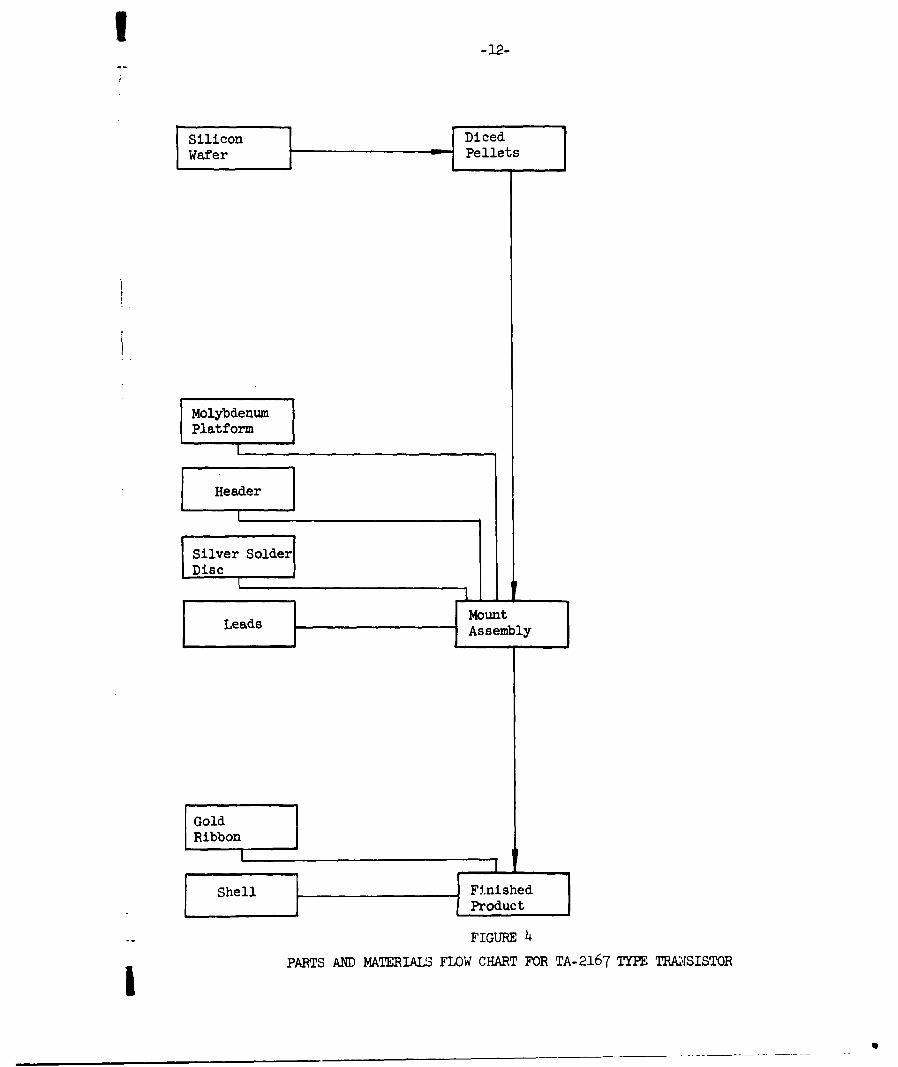
A. Parts and Materials
A flow chart of the major parts and materials used to fabricate the
TA-2167 transistor is shown in Figure 4. As detailed engineering drawings
and specifications for the major parts, assemblies,and sub-assemblies be-
come available, or are determined, these will be included in this section
of subsequent Quarterly Reports.
B. Processes and Processing
1. General
The tentative Process Flow Chart for the TA-2167 is shown in Fig-
ure 5. These processes are those which presently appear to be best
suited to produce this type of device in the required quantities. As
processes are modified, and equipment developed and put into operation,
the changes will be reported in this section of subsequent Quarterly
Reports. As the specific processes are optimized and standardized,
these standards will be reported. The general methods used to fabricate
* the TA-2167 are those applicable to a triple-diffused silicon mesa de-
* vice.
2. Diffusion
The impurity profile of a transistor suitable for high-voltage
applications is -hown in Figure 6. The surface concentration of the
base region (C1 ) is approximately an order of magnitude lower than the
emitter region. This determines the emitter breakdown voltage. A simple
double-diffused structure has a inherently high collector spreading resist-
ance. This condition leads to a higher saturation resistance than ex-
hibited by a single diffused device. Therefore, another N-type layer is
-12-
Wafer Pellets
MolybdenumPlatform
Header ]L
Silver SolderDisc
Leads Assembly
GoldRibbon
Shell Finished
Product
FIGURE 4
PARTS AND MATERIALS FLOW CHART FOR TA-2167 TYPE TRAISISTOR

w z
wI-Jr-
2woL L C'j
CL.
I O.O
jO
IJi_I 0
0d
1-U

ozz
zz
1z
_o 0-(-
I IF--
Id 0
(z
i:0u u

- 14-
I 1020 1
1019 PhosphorusjDiffused PhosphorusEmitter Diffused
Collector
1018
1 0 17 -B oronC1 Diffused
Co0 Base
1 14 0 16C
1 2 3 4 5 6
I - Distance (mils)
i FIGURE 6
IMPJRITY PROFILE FOR HIGH VOLTAGE SILICON TRANSISTORS
-15-
shown on the right side of the figure. This collector diffusion reduces
the collector spreading resistance and results in the final NPIN struct-
ure.
Several diffusion runs have been started in the Model Shop. These
runs are for the purpose of training operators, "debugging" the equip-
ment, and determining possible production problems.
3. Collector Formation
Only preliminary work has been done in this area.
~4. Base Formation
Only preliminary work has been done in this area.
5. Emitter Formation
Some work has been done in this area. The present photographic
plates permit only four units per wafer to be formed. It was felt that
this was insufficient for production quantities. As a result, the photo-
graphic plates have been redesigned to increase the number of units per
wafer. These redesigned plates will iecessitate changes in handling
equipment in order to realize the maximum benefit from the change. This
jwork is beginning.
6. Contacting
Only preliminary work has been done in this area.
7. Mesa Formation
Only preliminary work has been done in this area.
8. Dicing
Only preliminary work has been done in this area.
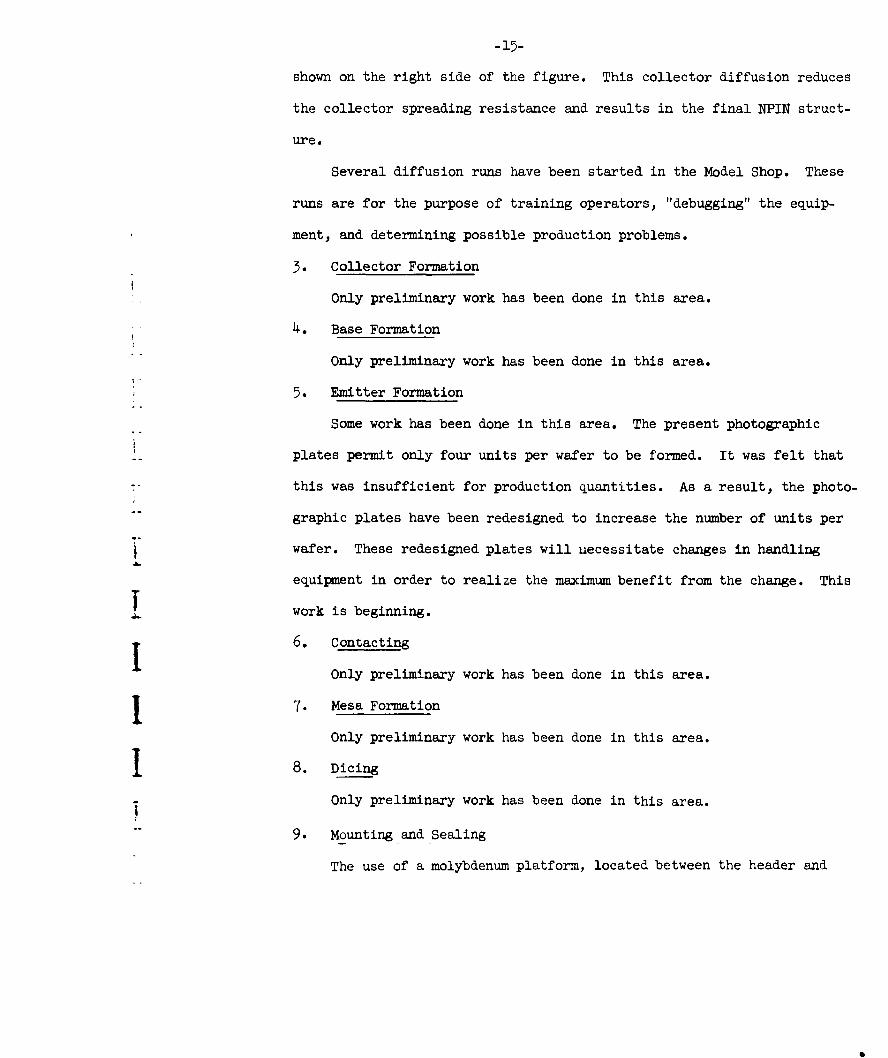
9. Mounting and Sealing
The use of a molybdenum platform, located between the header and

-16-
I the pellet, has been initiated. The thickness is to be 0.050" and will
permit the required brazing operation without introducing problems of
warping during subsequent operations. The noble metal braze used to
{ place the molybdenum platform on the header eliminates the need to
use a lead solder and thus permits higher temperature operation. Re-
Ilatively simple f±ixtures have been designed to accurately locate therplatform on the header during brazing. Figure 7 is a photograph of a
device showing the 0.050" molybdenum platform located on the header.
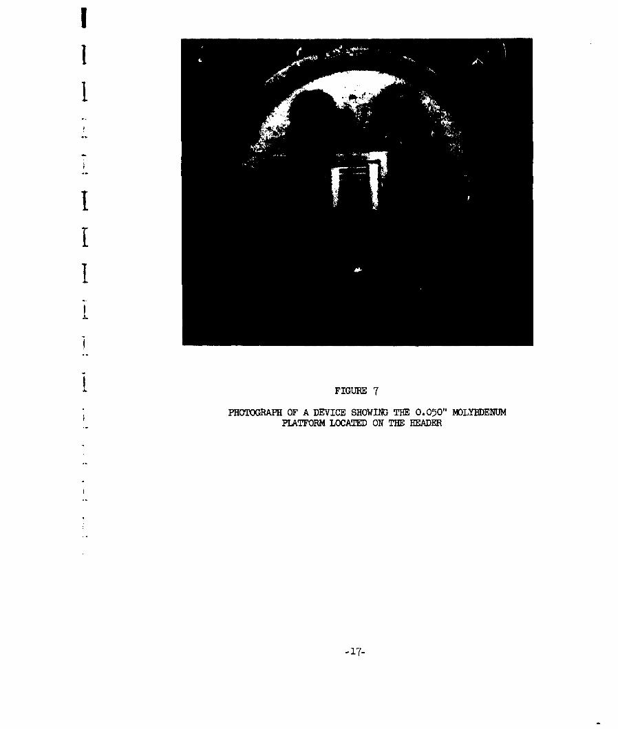
The connector leads which are used on this device are made of
0.005" x 0.020" gold ribbon. This ribbon has been found superior to
the previous wire because the thermocompression bonding operation is
simplified and produces a resultant reduction in fabrication time and
improvement in the quality of the bonds. It has also been found that
this lead material will conduct up to 25 amperes of current thus allow-
ing a good margin of safety for the 10 amperes required for this device.
Figure 8 is a photograph of a device with the gold ribbon leads.
I
11!I1.
117
1.
I
FIGURE 8
I PHOTOGRAPH OF A UNIT BOI~Ba USING TRE TWO GOLD RIBBONS
IIIIIIIIII

-19-
IV. DEVICE EVALUATION
A. Electrical
Five state-of-the-art samples were given to Mr. C. Fisher of the Signal
Corps on September 22, 1961. The electrical characteristics of these samples
are tabulated in Table I.
Voltage oICO§ ICEO 'ERO VCE(saLt) CrossoVerotg Co
at at at 0.1lA 1lA 5 A 10QA 0.5 A at1A with p±.f400 V 300 v 8 v 0.5 V lo V 4 v 5 A 4.20 pulse
138-9 0.7 0.6 o.16 25 45 58 12.5 0.20 100 182
138-5 o.4 0.15 o.8 30 11 110 12.0 0.27 90 201
135-2 4.0 4.0 0.3 50 59 63 12.0 0.22 90 165
135-5 1.4 1.0 0.00 20 56 56 10.0 0.25 90 171
135-6 O.O1 0.01 3.2 9 56 63 12.5 0.20 90 136
§ All current readings in ma I
TABLE I
ELECTRICAL CHARACTERISTICS OF INITIAL FIVE STATE-OF-THE-ART SAMPLES
Experiments on contact resistance have been performed in our laboratory.
Results as low as 0.25 0C/watt, with silicone grease applied between the
mating surfaces, have been obtained. An efficient heat sink, whose thermal
resistance is in the neighborhood of 0.2 0C/watt, may be obtained by using
the water-cooled method. Since "CA is the sum of the contact and heat sink
thermal resistances, in this case CA =0.25+ 0.2=0.450C/W,there seems to be
some inconsistency between this value and that specified in the detailed
operating life requirements for this contract. Work to resolve this apparent
inconsistency is continuing.
B. Environmental
Only preliminary work has been done in this area.
-20-
V. CONCLUSIONS
It is now possible to make, in the laboratory, devices which satisfy the
end requirements for circuitry. However, some development work is required be-
fore the model shop and pilot line are able to fabricate devices which can satisfy
the full contract reliability specifications for operating life, mechanical, and
I environmental tests.
A double-ended stud package has been proven feasible from a design point
of view.
Improvements in the mounting and bonding area have made the fabricated devices
more rugged.IIIIIIII

-21-
VI. PROGRAM FOR NEXT QUARTER
During the next quarter, the following work should be completed:4.
1. Evaluate the double-ended stud package regarding thermal resist-ance, quality of seal obtainable etc.;
2. Expand the Model Shop pilot line capability;
3. Improve the device yield to the high-current, high-voltagerequirement;
S~4. Design Jigs and fixtures for use in mechanical and environmentaltests;
5. Establish an operating point for the Operating Life Test. Thiswill depend upon the case-to-ambient allowance as determined bythe Contracting Agency and RCA.
IIIIILIT
-22-
* -VII. PERSONNEL AND MAN HOURS
VThe biographies of the personnel contributing directly to this program are
listed below. Table II is a tabulation of the Man Hours expended on this con-
tract during the First Quarter.
EITH E. LOOFBOURROW - Manager, Industrial Transistor Product Development
Mr. Loofbourrow received the BSEE degree from Oklahoma State University in
i1950. He joined RCA as an Engineering Trainee after college. He gained ex-
tensive knowledge and experience in receiving tubes and transistors during the
next five years as an application engineer and later as an engineering leader. He
was then promoted to Manager, Test Engineering for the Semiconductor Division
and served in that capacity until 1957.when he was promoted to the position of
- Manager, Industrial Application Engineering for the Semiconductor Division. Mr.
Loofbourrow was promoted to his present position in 1961, and the work done under
this contract will be administered by him.
Mr,.Loofbourrow has published extensively in various journals on the design
and application of various tubes and transistors.
GERALD J. AZNDESKIE - Manager, High-Frequency Silicon Model Shop
Mr. Andeskie received the B.S. degree in Engineering Administration from
Rutgers University. He joined the RCA Semiconductor Division in October, 1956
as Engineering Administrator to the Chief Engineer. He assumed his present position
on January 1, 1959. Prior tc coming with RCA, Mr. Andeskie served two years with
the U. S. Air Force as Aircraft Maintenance Engineering Officer and Production
- Control Officer. He also spent two years with the U. S. Gypsum Company as Project
Engineer.
ZUIK F. CHANG
Mr. Chang was born in Shanghai, China and came to this country where he
graduated from Rensselaer Polytechnic Institute in 1959 with a BEE degree. He
I, T-23-
joined the RCA Semiconductor and Materials Division in 1959 as an Enginelring
-. Trainee. Following his training he joined the Industrial Device Applications
Group as an application engineer. Mr. Chang will be doing much of the circuitry
work associated with this contract.
HERBERT R. MEISEL
Mr. Meisel received the B.M.E. degree from Rensselaer Institut3 in 1950.
He received the MS degree in Management Engineering from Newark College of Eng-
ineering in 1956 and the MS degree in Physics from Stevens Institute of Technology
in 1958. Mr. Meisel joined the RCA Semiconductor Division in 1953 as a design
and development engineer. His projects have included: germanium alloy audio and
power transistors, alloyed silicon rectifiers, Signal Corps micromodule transis-
Itors, Signal Corps Device 1 PNP germanium, and Devices 13, 14 and 15 NPN and PNPdiffused silicon transistors. These projects have included txtensive experience
in industrial preparedness studies. Prior to joining RCA, Mr. Meisel was anA-
Ordiance Test Engineer at Aberdeen Proving Grounds, Maryland and a Student Electronics
Officer in the U. S. Air Force. Mr. Meisel assumed his present duties as Group
Leader in October, 1960.
" - SEYMOUR SILVERSTEIN
Mr. Silverstein received the B.M.E.degree from City College of New York in
1951 and the B.E.E. degree from the same college in 1956. Mr. Silverstein joined
RCA as a Trainee in 1951 and worked in the Tube Division at Harrison, Lancaster
and Camden. Following his Trainee time he was assigned to Camden where he work.
"" ed on broadcast TV antennas as a design engineer. He joined the Semiconductor
Division and was assigned to the Development Shop in Harrison in 1951 and later
transferred to Somerville with this organization. During this time he developed,
refined, and optimized the processes for devices prior to having them transferred
to the factory. In 1959 he was transferred to the Semiconductor Model Shop where

-24-
he gained extensive knowledge about Pilot Production of devices. While there
Mr. Silverstein was also instrumental in training operators for the various pro-
cesses. In 1961 he was promoted to design engineering and assigned to the Industrial
Design group of the Semiconductor Division. Since that time he has been ra-
sponsible for the design and prototype work on several devices. Mr. Silverstein
is now a Senior Engineer with RCA.
Mr. Silverstein holds one patent for "Jig Alloying of Semiconductor Devices"i" (Patent No. z, 964, 431).
NORMAN C. TURNER
Mr. Turner received the B.S. degree in Mechanical Engineering from Rutgers
University in 1958. Prior to attending Rutgers, he was employed by the Service
Machine Co. as a tool and die maker and also did some tool and machine design
work. Following his graduation from Rutgers he was a rocket engine project eng-
ineer with the Reaction Motors Division of Thiokol Chemical Co. Mr. Turner was
an Ordiance Mechanical Engineering Officer in the U. S. Army from 1958 to 1959.
He joined RCA in December, 1959 and has been assigned to the Industrial Model Shop
since that time.
JEROME E. WRIGHT
Mr. Wright attended Wilkes College from 1952 to 1954, and received the B.S.E.E.
degree from Pennsylvania State University in 1956. He joined RCA in June, 1956
as a Trainee in the Training Program. Mr. Wright joined the Semiconductor Division
section as a device engineer. His projects have included: germanium alloy audio
- and power transistors, Signal Corps Device 1 PNP and NFN germanium transistors, low
and high power germanium transistors, and the triple diffused silicon high frequency
lifetest program. Mr. Wright has had extensive experience in industrial pre-
paredness studies programs.
-25-
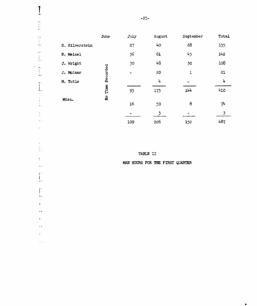
June July August September Total
S. Silverstein 27 40 68 135
H. Meisel 36 61 45 142
J. Wright 30 48 30 108
J. Molnar - 20 1 21
M. Tutle 4 - 4
93 173 144 41o
Misc..16 50 8 74
- 3 - 5109 226 152 487
TABLE II
MAN HOURS FOR THE FIRST QUARTER
1.
Related Documents