DAI0491A Copyright 2015 ARM. All rights reserved. i AN491 Non-confidential Application Note AN491 IoT Subsystem for Cortex-M Non-confidential

Welcome message from author
This document is posted to help you gain knowledge. Please leave a comment to let me know what you think about it! Share it to your friends and learn new things together.
Transcript
DAI0491A Copyright 2015 ARM. All rights reserved. iAN491 Non-confidential
Application Note AN491IoT Subsystem for Cortex-M
Non-confidential
DAI0491A Copyright 2015 ARM. All rights reserved. iiAN491 Non-confidential
IoT Subsystem for Cortex-M
Copyright © 2015 ARM. All rights reserved.
Release Information
The following changes have been made to this SMM.
Change History
Date Issue Confidentiality Change
25 September 2015 1 Non-confidential First release
Proprietary Notice
Words and logos marked with ™ or ® are registered trademarks or trademarks of ARM in the EU and other countries except
as otherwise stated below in this proprietary notice. Other brands and names mentioned herein may be the trademarks of
their respective owners.
Neither the whole nor any part of the information contained in, or the product described in, this document may be adapted
or reproduced in any material form except with the prior written permission of the copyright holder.
The product described in this document is subject to continuous developments and improvements. All particulars of the
product and its use contained in this document are given by ARM in good faith. However, all warranties implied or
expressed, including but not limited to implied warranties of merchantability, or fitness for purpose, are excluded.
This document is intended only to assist the reader in the use of the product. ARM shall not be liable for any loss or damage
arising from the use of any information in this document, or any error or omission in such information, or any incorrect use
of the product.
Where the term ARM is used it means “ARM or any of its subsidiaries as appropriate”.
Confidentiality Status
This document is Non-confidential. The right to use, copy and disclose this document may be subject to license restrictions
in accordance with the terms of the agreement entered into by ARM and the party that ARM delivered this document to.
Product Status
The information in this document is final, that is for a developed product .
Web Address
http://www.arm.com
DAI0491A Copyright 2015 ARM. All rights reserved. iiiAN491 Non-confidential
Contents
IoT Subsystem for Cortex-M1 Conventions and Feedback ....................................................................................1-1
2 Preface ......................................................................................................................2-1
2.1 References ..........................................................................................................2-1
2.2 Terms and abbreviations .....................................................................................2-1
2.3 Encryption key .....................................................................................................2-2
3 Overview ...................................................................................................................3-1
3.2 Detailed memory map .........................................................................................3-3
3.3 External ZBT Synchronous SRAM (SSRAM1)....................................................3-5
3.4 External ZBT Synchronous SRAM (SSRAM2 & SSRAM3) ................................3-5
3.5 External PSRAM..................................................................................................3-5
3.6 AHB GPIO ...........................................................................................................3-5
3.7 SPI (Serial Peripheral Interface)..........................................................................3-5
3.8 Color LCD parallel interface ................................................................................3-6
3.9 Ethernet ...............................................................................................................3-6
3.10 VGA .....................................................................................................................3-6
3.11 Audio I2S..............................................................................................................3-7
3.12 Audio Configuration .............................................................................................3-8
3.13 FPGA system control and I/O..............................................................................3-9
4 IO mapping ...............................................................................................................4-1
5 Clocks .......................................................................................................................5-1
6 Interrupt assignments .............................................................................................6-1
7 Serial Communication Controller (SCC)................................................................7-3
DAI0491A Copyright 2015 ARM. All rights reserved. 1-1AN491 Non-confidential
1 Conventions and Feedback
The following describes the typographical conventions and how to give feedback:
Typographical conventions
The following typographical conventions are used:
monospace denotes text that you can enter at the keyboard, such as commands, file andprogram names, and source code.
monospace denotes a permitted abbreviation for a command or option. You can enterthe underlined text instead of the full command or option name.
monospace italic
denotes arguments to commands and functions where the argument is to bereplaced by a specific value.
monospace bold
denotes language keywords when used outside example code.
italic highlights important notes, introduces special terminology, denotes internalcross-references, and citations.
bold highlights interface elements, such as menu names. Denotes signal names.Also used for emphasis in descriptive lists, where appropriate.
Feedback on this product
If you have any comments and suggestions about this product, contact your supplier and give:
Your name and company.
The serial number of the product.
Details of the release you are using.
Details of the platform you are using, such as the hardware platform, operating system type andversion.
A small standalone sample of code that reproduces the problem.
A clear explanation of what you expected to happen, and what actually happened.
The commands you used, including any command-line options.
Sample output illustrating the problem.
The version string of the tools, including the version number and build numbers.
Feedback on documentation
If you have comments on the documentation, e-mail [email protected]. Give:
The title.
The number, DAI0491A.
If viewing online, the topic names to which your comments apply.
If viewing a PDF version of a document, the page numbers to which your comments apply.
A concise explanation of your comments.
ARM also welcomes general suggestions for additions and improvements.

DAI0491A Copyright 2015 ARM. All rights reserved. 1-2AN491 Non-confidential
ARM periodically provides updates and corrections to its documentation on the ARM InformationCenter, together with knowledge articles and Frequently Asked Questions (FAQs).
Other information
ARM Information Center, http://infocenter.arm.com/help/index.jsp.
ARM Technical Support Knowledge Articles,http://infocenter.arm.com/help/topic/com.arm.doc.faqs/index.html.
ARM Support and Maintenance, http://www.arm.com/support/services/support-maintenance.php.
ARM Glossary, http://infocenter.arm.com/help/topic/com.arm.doc.aeg0014-/index.html.
The ARM Glossary is a list of terms used in ARM documentation, together with definitions forthose terms. The ARM Glossary does not contain terms that are industry standard unless the ARMmeaning differs from the generally accepted meaning.
DAI0491A Copyright 2015 ARM. All rights reserved. 2-1AN491 Non-confidential
2 Preface
This SMM is intended for developers/programmers/users who deploy hardware/software for apurpose.
These topics support the following chapters:
References on page 2-1.
Terms and abbreviations on page 2-1.
Encryption key on page 2-2
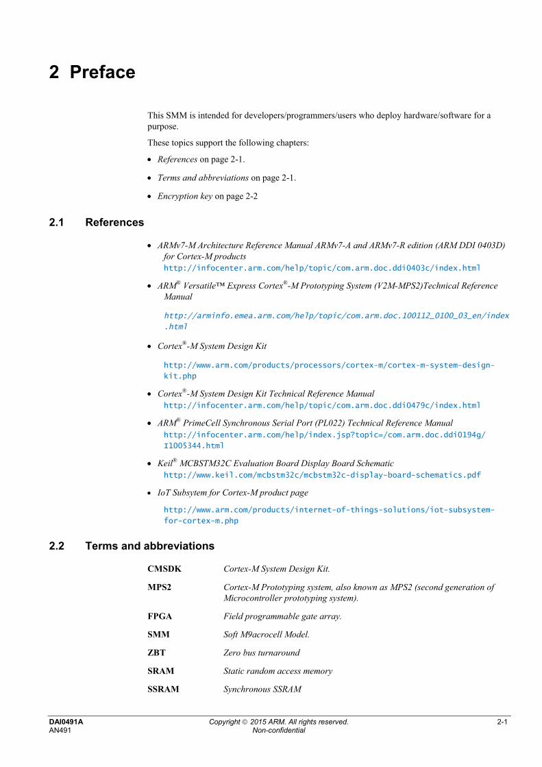
2.1 References
ARMv7-M Architecture Reference Manual ARMv7-A and ARMv7-R edition (ARM DDI 0403D)for Cortex-M products
http://infocenter.arm.com/help/topic/com.arm.doc.ddi0403c/index.html
ARM® Versatile™ Express Cortex®-M Prototyping System (V2M-MPS2)Technical ReferenceManual
http://arminfo.emea.arm.com/help/topic/com.arm.doc.100112_0100_03_en/index
.html
Cortex®-M System Design Kit
http://www.arm.com/products/processors/cortex-m/cortex-m-system-design-
kit.php
Cortex®-M System Design Kit Technical Reference Manual
http://infocenter.arm.com/help/topic/com.arm.doc.ddi0479c/index.html
ARM® PrimeCell Synchronous Serial Port (PL022) Technical Reference Manual
http://infocenter.arm.com/help/index.jsp?topic=/com.arm.doc.ddi0194g/
I1005344.html
Keil® MCBSTM32C Evaluation Board Display Board Schematic
http://www.keil.com/mcbstm32c/mcbstm32c-display-board-schematics.pdf
IoT Subsytem for Cortex-M product page
http://www.arm.com/products/internet-of-things-solutions/iot-subsystem-
for-cortex-m.php
2.2 Terms and abbreviations
CMSDK Cortex-M System Design Kit.
MPS2 Cortex-M Prototyping system, also known as MPS2 (second generation ofMicrocontroller prototyping system).
FPGA Field programmable gate array.
SMM Soft M9acrocell Model.
ZBT Zero bus turnaround
SRAM Static random access memory
SSRAM Synchronous SSRAM
DAI0491A Copyright 2015 ARM. All rights reserved. 2-2AN491 Non-confidential
2.3 Encryption key
ARM supplies the V2M-MPS2 motherboard with a decryption key programmed into the FPGA.This key is needed to enable loading of encrypted, prebuilt images. AN491 is supplied as anencrypted image.
Caution
A battery supplies power to the key storage area of the FPGA. Any keys stored in the FPGAmay be lost when battery power is lost. If this happens you must return the board to ARM forreprogramming of the key.

DAI0491A Copyright 2015 ARM. All rights reserved. 3-1AN491 Non-confidential
3 Overview
The SMM design is based on the IOT Subsystem for Cortex-M and incorporates a Cortex-M3processor. Cortex-M System Design Kit (CMSDK) components are used for many of theperipherals.
3.1.1 Overview
IoT Subsystem for Cortex-M CSSAPB Interface
GP
IO
GP
IO
GP
IO
GP
IO
Syste
mC
ontro
ler
SRAM
AHB to ZBTSRAM 64
AHB to ext SRAM
AHBto
APB
SPI x 2(master)
SBCon x 2
AudioI2S
FPGA IOregs
VGA(EDK)
AHB to ZBTSRAM 32
ZBT ZBT PSRAM Ethernet
SPI
APB
MCC
Initialisation
SCC
SPI
SCC
UART
Dual Timer
Watchdog
Core APB Peripherals
AHB Mux
AN491 Wrapper
DATARAM0
DATARAM1
SRAM0
SRAM1
SRAM2
SRAM3
ZBT ZBT
SRAM0IFSRAM1IF
SRAM2IFSRAM3IFFCACHERAM
FLASHInterface
AHB to ZBTSRAM 32
Other Peripherals
AHB
AHB
MPS2 or MPS2+ Board
Figure 3-1 System Overview

DAI0491A Copyright 2015 ARM. All rights reserved. 3-2AN491 Non-confidential
3.1.2 IoT Subsystem for Cortex-M diagram
PILSWJ/DP
TPIU
CM3
D SI
Code MUX
Multilayer AHB Bus MatrixAHB2APB
Bridge
AHB2SRAM3
IOT Subsystem for Cortex-M CSS
INITCM3S
AHB lite32-bit
WIC
FlashCache
APB4
TIMER0/1
….
TARGEXP1
TARGEXP0INITEXP0INITEXP1
TARG_SRAM3
INITCM3DI
SRAM3IF
TPIU
DAP
APBTARGEXP(APB4x11)2,4-8,11-15
AHB lite32-bit
AHB lite32-bit
TARG_SRAM2TARG_SRAM1TARG_SRAM0
SL AHB lite32-bit
SRAM2IFSRAM1IFSRAM0IF
AHB2SRAM2
AHB2SRAM1
AHB2SRAM0
AHB lite32-bit
AHB lite32-bit
AHB lite32-bit
AHB lite32-bit
AHB lite32-bit
MS AHBlite 32-bit
SL AHB lite32-bit
MS AHBlite 32-bit
AHB lite128-bit
SRAMController
SRAM128-bit
AHB lite32-bit
TARGAPB0
TARG_FLASH0
AHB lite32-bit
FiFigure 3-2 IoT Subsystem for Cortex-M Overview
3.1.3 Subsystem version
The IoT subsystem for Cortex-M implementation used in AN491 has been modified to replace itsFLASH memory controller with an SRAM controller for FPGA compatibility.

DAI0491A Copyright 2015 ARM. All rights reserved. 3-3AN491 Non-confidential
3.2 Detailed memory map
Start Address End Address Description Comment
0x60000000 0x5FFFFFFF Reserved
0x41100000 0x4113FFFF VGA Image 512x128x32bit
0x41010000 0x410FFFFF Reserved
0x41000000 0x4100FFFF VGA Console
0x40200000 0x40FFFFFF Ethernet via ahb_to_extmem16
0x40032000 0x401FFFFF Reserved
0x40031000 0x40031FFF GPIO5
0x40030000 0x40030FFF GPIO4
0x4002F000 0x4002FFFF SCC register See SCC section
0x40029000 0x4002EFFF Reserved
0x40028000 0x40028FFF FPGA System Control & I/O
0x40025000 0x40027FFF Reserved
0x40024000 0x40024FFF Audio I2S
0x40023000 0x40023FFF SBCon Audio Configuration
0x40022000 0x40022FFF SBCon Touch for LCD module
0x40021000 0x40021FFF PL022 SPI for LCD module
0x40020000 0x40020FFF PL022 SPI connector J21
0x4001F000 0x4001FFFF SysCtrl CMSDK system controller
0x40012000 0x4001EFFF Reserved
0x40011000 0x40011FFF GPIO1
0x40010000 0x40010FFF GPIO0
0x4000F000 0x40009FFF Reserved
0x40008000 0x40008FFF Watchdog
0x40006000 0x40007FFF Reserved
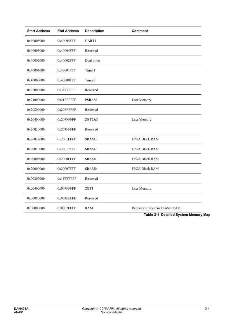
DAI0491A Copyright 2015 ARM. All rights reserved. 3-4AN491 Non-confidential
Start Address End Address Description Comment
0x40005000 0x40005FFF UART1
0x40003000 0x40004FFF Reserved
0x40002000 0x40002FFF Dual timer
0x40001000 0x40001FFF Timer1
0x40000000 0x40000FFF Timer0
0x22000000 0x3FFFFFFF Reserved
0x21000000 0x21FFFFFF PSRAM User Memory
0x20800000 0x20FFFFFF Reserved
0x20400000 0x207FFFFF ZBT2&3 User Memory
0x20020000 0x203FFFFF Reserved
0x20018000 0x2001FFFF SRAM3 FPGA Block RAM
0x20010000 0x20017FFF SRAM2 FPGA Block RAM
0x20008000 0x2000FFFF SRAM1 FPGA Block RAM
0x20000000 0x20007FFF SRAM0 FPGA Block RAM
0x00800000 0x1FFFFFFF Reserved
0x00400000 0x007FFFFF ZBT1 User Memory
0x00080000 0x003FFFFF Reserved
0x00000000 0x0007FFFF RAM Replaces subsystem FLASH RAM
Table 3-1 Detailed System Memory Map
DAI0491A Copyright 2015 ARM. All rights reserved. 3-5AN491 Non-confidential
3.3 External ZBT Synchronous SRAM (SSRAM1)
This is interfaced to two external 32-bit ZBT SSRAM in parallel, forming a 64-bit ZBT SSRAM.This memory is in the processor’s code region.
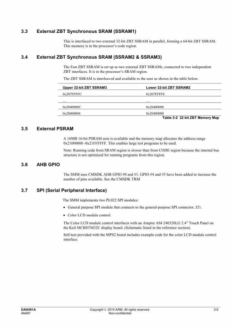
3.4 External ZBT Synchronous SRAM (SSRAM2 & SSRAM3)
The Fast ZBT SSRAM is set up as two external ZBT SSRAMs, connected to two independentZBT interfaces. It is in the processor’s SRAM region.
The ZBT SSRAM is interleaved and available to the user as shown in the table below.
Upper 32-bit ZBT SSRAM3 Lower 32-bit ZBT SSRAM2
0x207FFFFC 0x207FFFF8
… …
0x2040000C 0x20400008
0x20400004 0x20400000Table 3-2 32 bit ZBT Memory Map
3.5 External PSRAM
A 16MB 16-bit PSRAM area is available and the memory map allocates the address-range0x21000000 -0x21FFFFFF. This enables large test programs to be used.
Note: Running code from SRAM region is slower than from CODE region because the internal busstructure is not optimized for running programs from this region.
3.6 AHB GPIO
The SMM uses CMSDK AHB GPIO #0 and #1. GPIO #4 and #5 have been added to increase thenumber of pins available. See the CMSDK TRM
3.7 SPI (Serial Peripheral Interface)
The SMM implements two PL022 SPI modules:
General purpose SPI module that connects to the general-purpose SPI connector, J21.
Color LCD module control.
The Color LCD module control interfaces with an Ampire AM-240320LG 2.4” Touch Panel onthe Keil MCBSTM32C display board. (Schematic listed in the reference section).
Self-test provided with the MPS2 board includes example code for the color LCD module controlinterface.
DAI0491A Copyright 2015 ARM. All rights reserved. 3-6AN491 Non-confidential
3.8 Color LCD parallel interface
The color LCD module has two interfaces:
SPI for LCD module used for sending image data to the LCD.
I2C for touch used to transfer data input via the touch screen.
These interfaces are connected to a STMicroelectronics STMPE811QTR Port Expander withAdvanced Touch Screen Controller on the Keil MCBSTM32C display board. (Schematic listed inthe reference section).
Self-test provided with the MPS2 includes example code for both of these interfaces.
3.9 Ethernet
The SMM design connects SMSC LAN9220 through AHB to external memory block.
The SMM self-test code includes example code for a simple loopback operation.
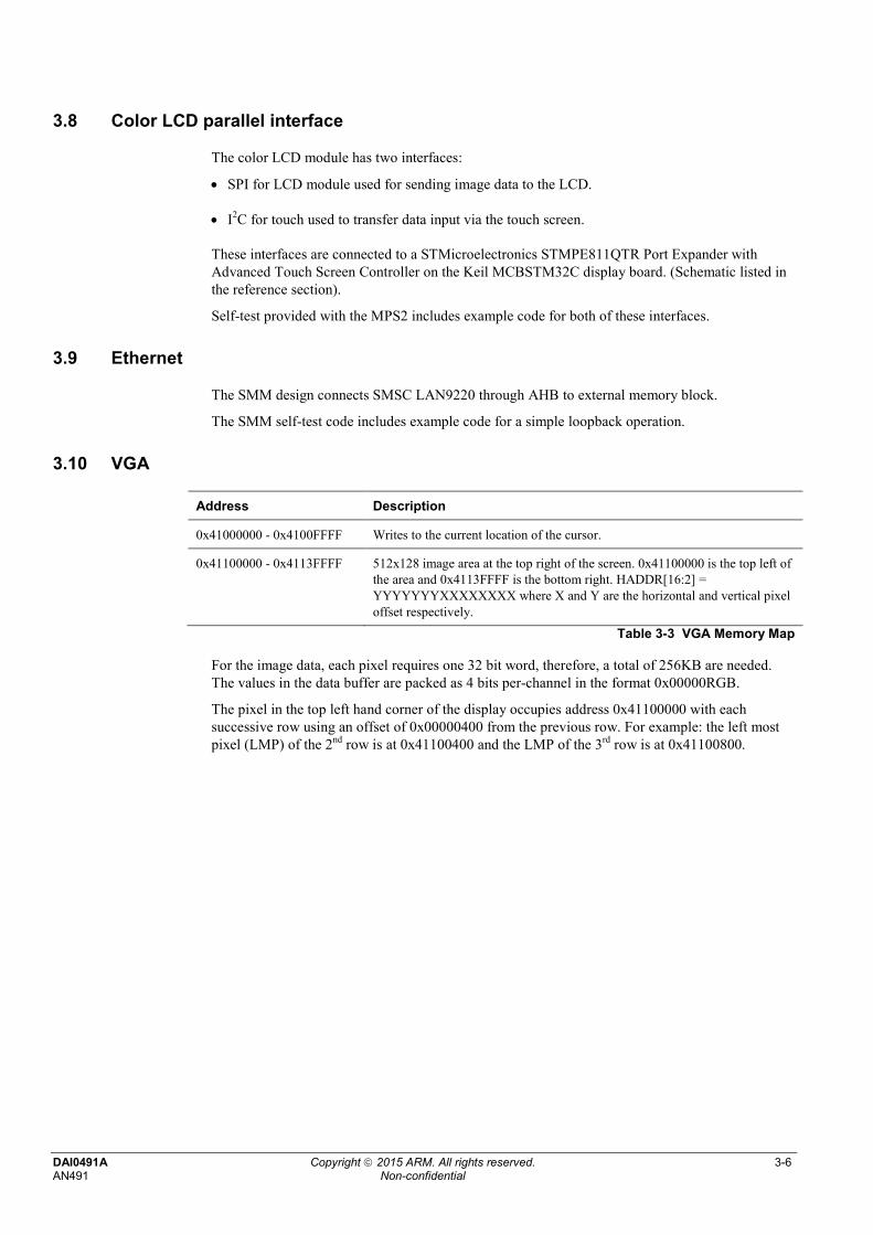
3.10 VGA
Address Description
0x41000000 - 0x4100FFFF Writes to the current location of the cursor.
0x41100000 - 0x4113FFFF 512x128 image area at the top right of the screen. 0x41100000 is the top left ofthe area and 0x4113FFFF is the bottom right. HADDR[16:2] =YYYYYYYXXXXXXXX where X and Y are the horizontal and vertical pixeloffset respectively.
Table 3-3 VGA Memory Map
For the image data, each pixel requires one 32 bit word, therefore, a total of 256KB are needed.The values in the data buffer are packed as 4 bits per-channel in the format 0x00000RGB.
The pixel in the top left hand corner of the display occupies address 0x41100000 with eachsuccessive row using an offset of 0x00000400 from the previous row. For example: the left mostpixel (LMP) of the 2nd row is at 0x41100400 and the LMP of the 3rd row is at 0x41100800.
DAI0491A Copyright 2015 ARM. All rights reserved. 3-7AN491 Non-confidential
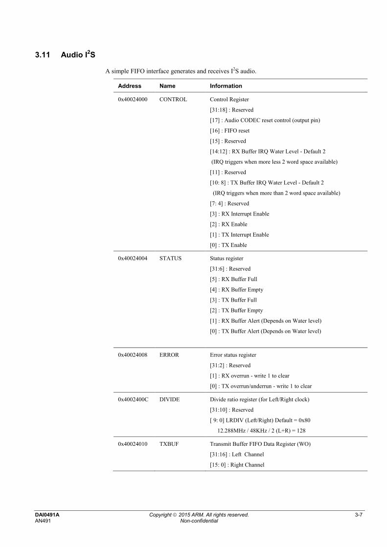
3.11 Audio I2S
A simple FIFO interface generates and receives I2S audio.
Address Name Information
0x40024000 CONTROL Control Register
[31:18] : Reserved
[17] : Audio CODEC reset control (output pin)
[16] : FIFO reset
[15] : Reserved
[14:12] : RX Buffer IRQ Water Level - Default 2
(IRQ triggers when more less 2 word space available)
[11] : Reserved
[10: 8] : TX Buffer IRQ Water Level - Default 2
(IRQ triggers when more than 2 word space available)
[7: 4] : Reserved
[3] : RX Interrupt Enable
[2] : RX Enable
[1] : TX Interrupt Enable
[0] : TX Enable
0x40024004 STATUS Status register
[31:6] : Reserved
[5] : RX Buffer Full
[4] : RX Buffer Empty
[3] : TX Buffer Full
[2] : TX Buffer Empty
[1] : RX Buffer Alert (Depends on Water level)
[0] : TX Buffer Alert (Depends on Water level)
0x40024008 ERROR Error status register
[31:2] : Reserved
[1] : RX overrun - write 1 to clear
[0] : TX overrun/underrun - write 1 to clear
0x4002400C DIVIDE Divide ratio register (for Left/Right clock)
[31:10] : Reserved
[ 9: 0] LRDIV (Left/Right) Default = 0x80
12.288MHz / 48KHz / 2 (L+R) = 128
0x40024010 TXBUF Transmit Buffer FIFO Data Register (WO)
[31:16] : Left Channel
[15: 0] : Right Channel
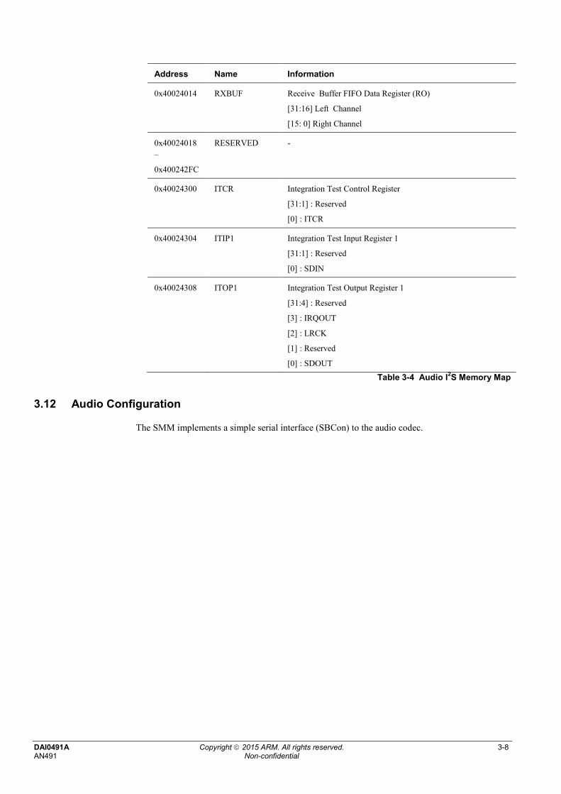
DAI0491A Copyright 2015 ARM. All rights reserved. 3-8AN491 Non-confidential
Address Name Information
0x40024014 RXBUF Receive Buffer FIFO Data Register (RO)
[31:16] Left Channel
[15: 0] Right Channel
0x40024018
–
0x400242FC
RESERVED -
0x40024300 ITCR Integration Test Control Register
[31:1] : Reserved
[0] : ITCR
0x40024304 ITIP1 Integration Test Input Register 1
[31:1] : Reserved
[0] : SDIN
0x40024308 ITOP1 Integration Test Output Register 1
[31:4] : Reserved
[3] : IRQOUT
[2] : LRCK
[1] : Reserved
[0] : SDOUT
Table 3-4 Audio I2S Memory Map
3.12 Audio Configuration
The SMM implements a simple serial interface (SBCon) to the audio codec.
DAI0491A Copyright 2015 ARM. All rights reserved. 3-9AN491 Non-confidential
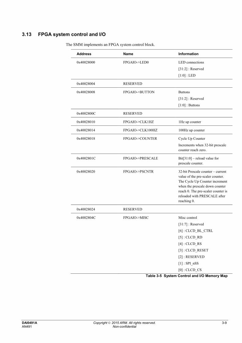
3.13 FPGA system control and I/O
The SMM implements an FPGA system control block.
Address Name Information
0x40028000 FPGAIO->LED0 LED connections
[31:2] : Reserved
[1:0] : LED
0x40028004 RESERVED
0x40028008 FPGAIO->BUTTON Buttons
[31:2] : Reserved
[1:0] : Buttons
0x4002800C RESERVED
0x40028010 FPGAIO->CLK1HZ 1Hz up counter
0x40028014 FPGAIO->CLK100HZ 100Hz up counter
0x40028018 FPGAIO->COUNTER Cycle Up Counter
Increments when 32-bit prescale
counter reach zero.
0x4002801C FPGAIO->PRESCALE Bit[31:0] – reload value for
prescale counter.
0x40028020 FPGAIO->PSCNTR 32-bit Prescale counter – current
value of the pre-scaler counter.
The Cycle Up Counter increment
when the prescale down counter
reach 0. The pre-scaler counter is
reloaded with PRESCALE after
reaching 0.
0x40028024 RESERVED
0x4002804C FPGAIO->MISC Misc control
[31:7] : Reserved
[6] : CLCD_BL_CTRL
[5] : CLCD_RD
[4] : CLCD_RS
[3] : CLCD_RESET
[2] : RESERVED
[1] : SPI_nSS
[0] : CLCD_CS
Table 3-5 System Control and I/O Memory Map
DAI0491A Copyright 2015 ARM. All rights reserved. 4-1AN491 Non-confidential
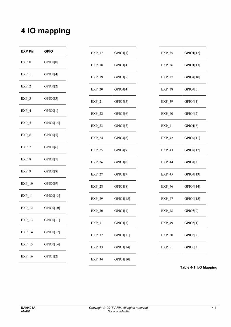
4 IO mapping
EXP Pin GPIO
EXP_0 GPIO0[0]
EXP_1 GPIO0[4]
EXP_2 GPIO0[2]
EXP_3 GPIO0[3]
EXP_4 GPIO0[1]
EXP_5 GPIO0[15]
EXP_6 GPIO0[5]
EXP_7 GPIO0[6]
EXP_8 GPIO0[7]
EXP_9 GPIO0[8]
EXP_10 GPIO0[9]
EXP_11 GPIO0[13]
EXP_12 GPIO0[10]
EXP_13 GPIO0[11]
EXP_14 GPIO0[12]
EXP_15 GPIO0[14]
EXP_16 GPIO1[2]
EXP_17 GPIO1[3]
EXP_18 GPIO1[4]
EXP_19 GPIO1[5]
EXP_20 GPIO4[4]
EXP_21 GPIO4[5]
EXP_22 GPIO4[6]
EXP_23 GPIO4[7]
EXP_24 GPIO4[8]
EXP_25 GPIO4[9]
EXP_26 GPIO1[0]
EXP_27 GPIO1[9]
EXP_28 GPIO1[8]
EXP_29 GPIO1[15]
EXP_30 GPIO1[1]
EXP_31 GPIO1[7]
EXP_32 GPIO1[11]
EXP_33 GPIO1[14]
EXP_34 GPIO1[10]
EXP_35 GPIO1[12]
EXP_36 GPIO1[13]
EXP_37 GPIO4[10]
EXP_38 GPIO4[0]
EXP_39 GPIO4[1]
EXP_40 GPIO4[2]
EXP_41 GPIO1[6]
EXP_42 GPIO4[11]
EXP_43 GPIO4[12]
EXP_44 GPIO4[3]
EXP_45 GPIO4[13]
EXP_46 GPIO4[14]
EXP_47 GPIO4[15]
EXP_48 GPIO5[0]
EXP_49 GPIO5[1]
EXP_50 GPIO5[2]
EXP_51 GPIO5[3]
Table 4-1 I/O Mapping
DAI0491A Copyright 2015 ARM. All rights reserved. 5-1AN491 Non-confidential
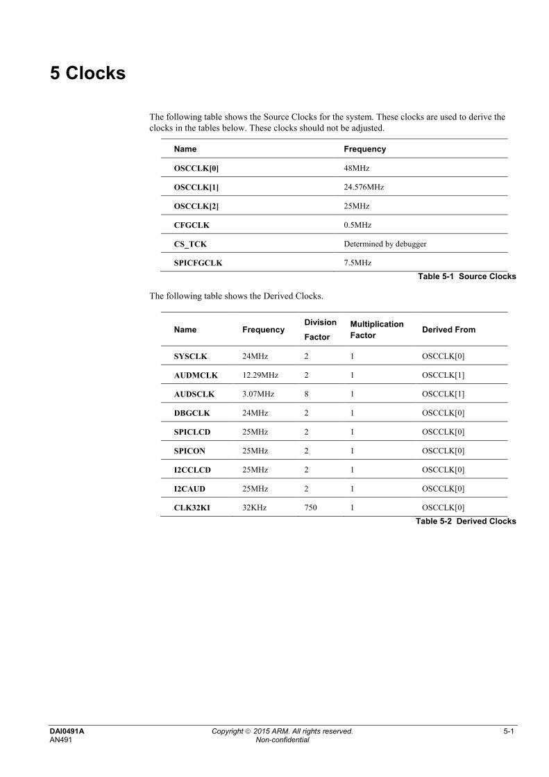
5 Clocks
The following table shows the Source Clocks for the system. These clocks are used to derive theclocks in the tables below. These clocks should not be adjusted.
Name Frequency
OSCCLK[0] 48MHz
OSCCLK[1] 24.576MHz
OSCCLK[2] 25MHz
CFGCLK 0.5MHz
CS_TCK Determined by debugger
SPICFGCLK 7.5MHz
Table 5-1 Source Clocks
The following table shows the Derived Clocks.
Name FrequencyDivision
Factor
Multiplication
FactorDerived From
SYSCLK 24MHz 2 1 OSCCLK[0]
AUDMCLK 12.29MHz 2 1 OSCCLK[1]
AUDSCLK 3.07MHz 8 1 OSCCLK[1]
DBGCLK 24MHz 2 1 OSCCLK[0]
SPICLCD 25MHz 2 1 OSCCLK[0]
SPICON 25MHz 2 1 OSCCLK[0]
I2CCLCD 25MHz 2 1 OSCCLK[0]
I2CAUD 25MHz 2 1 OSCCLK[0]
CLK32KI 32KHz 750 1 OSCCLK[0]
Table 5-2 Derived Clocks
DAI0491A Copyright 2015 ARM. All rights reserved. 6-1AN491 Non-confidential
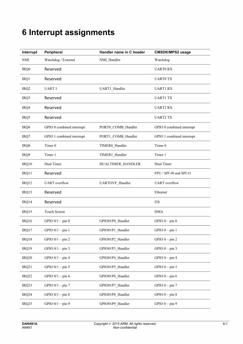
6 Interrupt assignments
Interrupt Peripheral Handler name in C header CMSDK/MPS2 usage
NMI Watchdog / External NMI_Handler Watchdog
IRQ0 Reserved UART0 RX
IRQ1 Reserved UART0 TX
IRQ2 UART 1 UART1_Handler UART1 RX
IRQ3 Reserved UART1 TX
IRQ4 Reserved UART2 RX
IRQ5 Reserved UART2 TX
IRQ6 GPIO 0 combined interrupt PORT0_COMB_Handler GPIO 0 combined interrupt
IRQ7 GPIO 1 combined interrupt PORT1_COMB_Handler GPIO 1 combined interrupt
IRQ8 Timer 0 TIMER0_Handler Timer 0
IRQ9 Timer 1 TIMER1_Handler Timer 1
IRQ10 Dual Timer DUALTIMER_HANDLER Dual Timer
IRQ11 Reserved FPU / SPI #0 and SPI #1
IRQ12 UART overflow UARTOVF_Handler UART overflow
IRQ13 Reserved Ethernet
IRQ14 Reserved I2S
IRQ15 Touch Screen DMA
IRQ16 GPIO 0/1 – pin 0 GPIO01P0_Handler GPIO 0 – pin 0
IRQ17 GPIO 0/1 – pin 1 GPIO01P1_Handler GPIO 0 – pin 1
IRQ18 GPIO 0/1 – pin 2 GPIO01P2_Handler GPIO 0 – pin 2
IRQ19 GPIO 0/1 – pin 3 GPIO01P3_Handler GPIO 0 – pin 3
IRQ20 GPIO 0/1 – pin 4 GPIO01P4_Handler GPIO 0 – pin 4
IRQ21 GPIO 0/1 – pin 5 GPIO01P5_Handler GPIO 0 – pin 5
IRQ22 GPIO 0/1 – pin 6 GPIO01P6_Handler GPIO 0 – pin 6
IRQ23 GPIO 0/1 – pin 7 GPIO01P7_Handler GPIO 0 – pin 7
IRQ24 GPIO 0/1 – pin 8 GPIO01P8_Handler GPIO 0 – pin 8
IRQ25 GPIO 0/1 – pin 9 GPIO01P9_Handler GPIO 0 – pin 9
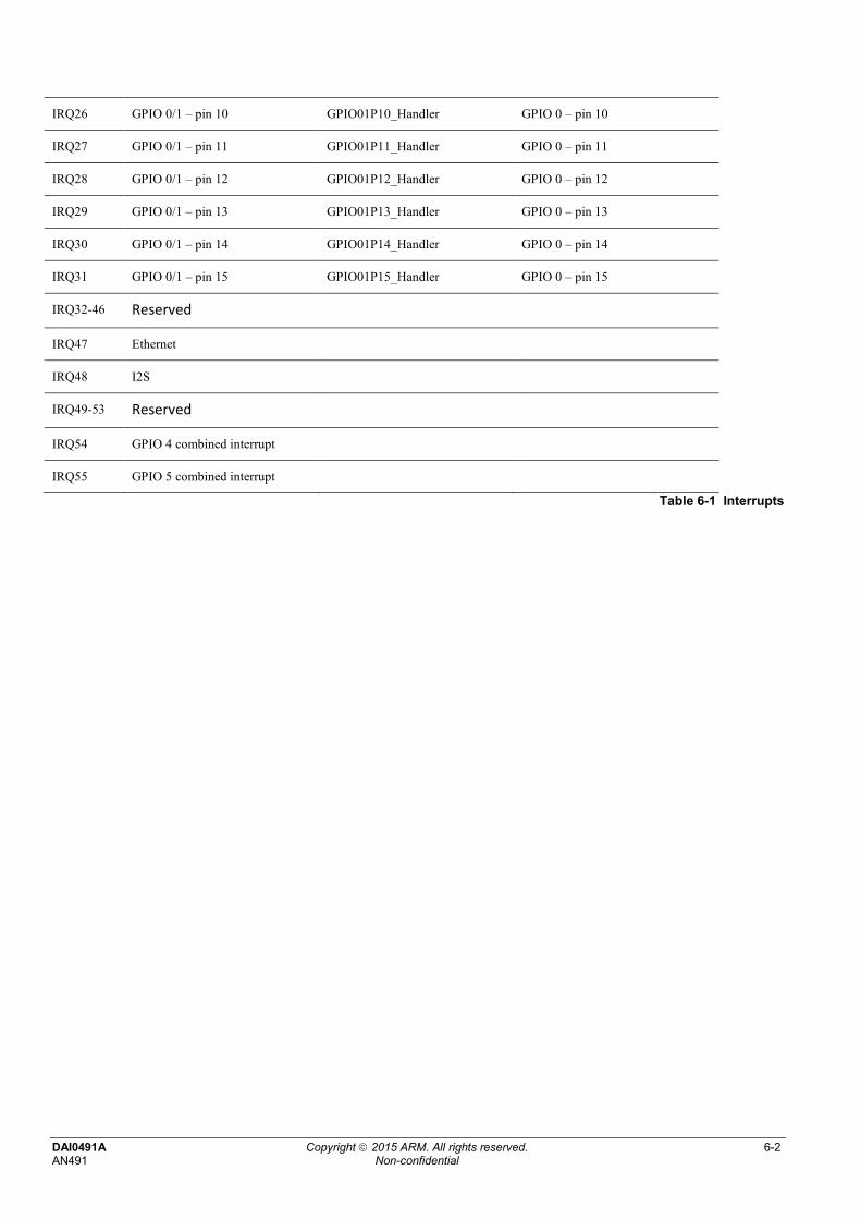
DAI0491A Copyright 2015 ARM. All rights reserved. 6-2AN491 Non-confidential
IRQ26 GPIO 0/1 – pin 10 GPIO01P10_Handler GPIO 0 – pin 10
IRQ27 GPIO 0/1 – pin 11 GPIO01P11_Handler GPIO 0 – pin 11
IRQ28 GPIO 0/1 – pin 12 GPIO01P12_Handler GPIO 0 – pin 12
IRQ29 GPIO 0/1 – pin 13 GPIO01P13_Handler GPIO 0 – pin 13
IRQ30 GPIO 0/1 – pin 14 GPIO01P14_Handler GPIO 0 – pin 14
IRQ31 GPIO 0/1 – pin 15 GPIO01P15_Handler GPIO 0 – pin 15
IRQ32-46 Reserved
IRQ47 Ethernet
IRQ48 I2S
IRQ49-53 Reserved
IRQ54 GPIO 4 combined interrupt
IRQ55 GPIO 5 combined interrupt
Table 6-1 Interrupts

DAI0491A Copyright 2015 ARM. All rights reserved. 7-3AN491 Non-confidential
7 Serial Communication Controller (SCC)
The SMM implements communication between the microcontroller and the FPGA system throughan SCC interface.
Figure 7-1 Diagram of the SCC Interface
The read-addresses and write-addresses of the SCC interface do not use bits[1:0].All address words are word-aligned.
Address Name Information
0x000 CFG_REG0 Bits[31:0] Reserved
0x004 CFG_REG1 Bits [31:8] Reserved
Bits [7:0] MCC LEDs: 0 = OFF 1 = ON
0x008 CFG_REG2 Reserved
0x00C CFG_REG3 Bits [31:8] Reserved
Bits [7:0] MCC switches: 0 = OFF 1 = ON
0x010 CFG_REG4 Bits [31:4] Reserved
Bits [3:0] Board Revision
0x014 CFG_REG5 Reserved
0x018 CFG_REG6 Reserved
0x01C CFG_REG7 Reserved
0x020 – 0x09C RESERVED -
0x0A0 SYS_CFGDATA_RTN 32bit DATA [r/w]
0x0A4 SYS_CFGDATA_OUT 32bit DATA [r/w]

DAI0491A Copyright 2015 ARM. All rights reserved. 7-4AN491 Non-confidential
Address Name Information
0x0A8 SYS_CFGCTRL Bit[31] : Start (generates interrupt on write to this
bit)
Bit[30] : R/W access
Bits[29:26] : Reserved
Bits[25:20] : Function value
Bits[19:12] : Reserved
Bits[11:0] : Device (value of 0/1/2 for supported
clocks)
0x0AC SYS_CFGSTAT Bit 0 : Complete
Bit 1 : Error
0x0AD – 0x0FC RESERVED -
0x100 SCC_DLL DLL lock register
Bits [31:24] DLL LOCK MASK[7:0] - These bits
indicate if the DLL locked is masked.
Bits [23:16] DLL LOCK MASK[7:0] - These bits
indicate if the DLLs are locked or unlocked.
Bits [15:1] : Reserved
Bit[0] This bit indicates if all enabled DLLs arelocked:
0x104 – 0xFF4 RESERVED -
0xFF8 SCC_AID SCC AID register is read only
Bits[31:24] : FPGA build number
Bits[23:20] : V2M-MPS2 target board revision
1 = (B) V2M-MPS2, 2 = (C) V2M-MPS2+
Bits[19:8] Reserved
Bits[7:0] number of SCC configuration register
0xFFC SCC_ID SCC ID register is read only
Bits[31:24] : Implementer ID: 0x41 = ARM
Bits[23:20] : Application note IP variant number(note 1)
Bits[19:16] : IP Architecture: 0x4 =AHB
Bits[11:4] : Primary part number: 491 = AN491
Bits[3:0] : Application note IP revision number(note 1)
Table 7-1 SCC Register memory map
note 1 The variant and revision numbers relate to the rxpy number. For example for r1p0 processors the 1 would
be the variant number and the 0 would be the revision number.
Related Documents