ANALYSIS AND CLASSIFICATION OF MICROPROGRAMMED COMPUTERS by Bing Ho Yee SUBMITTED IN PARTIAL FULFILLMENT OF THE REQUIREMENTS FOR THE DEGREES OF BACHELOR OF SCIENCE and MASTER OF SCIENCE at the MASSACHUSETTS INSTITUTE OF TECHNOLOGY June, 1972 Signature of Author Department of Elect cal En eering, May 1 Certified by-, hsi s Superykftor Arc ' 1ss. 9 JUN 27 1972

Welcome message from author
This document is posted to help you gain knowledge. Please leave a comment to let me know what you think about it! Share it to your friends and learn new things together.
Transcript
ANALYSIS AND CLASSIFICATION OF MICROPROGRAMMED COMPUTERS
by
Bing Ho Yee
SUBMITTED IN PARTIAL FULFILLMENT OF THE
REQUIREMENTS FOR THE DEGREES OF
BACHELOR OF SCIENCE
and
MASTER OF SCIENCE
at the
MASSACHUSETTS INSTITUTE OF TECHNOLOGY
June, 1972
Signature of AuthorDepartment of Elect cal En eering, May 1
Certified by-,hsi s Superykftor
Arc '1ss. 9
JUN 27 1972
2
ANALYSIS AND CLASSIFICATION OF MICROPROGRAMMED COMPUTERS
by
Bing Ho Yee
Submitted to the Department of Electrical Engineering on
May 12, 1972 in partial fulfillment of the requirements
for the Degrees of Bachelor of Science and Master of
Science.
ABSTRACT
A representation scheme is developed to represent
microprogrammed computers for easy comparison. Design
trade-off issues on ROM word dimensions, control store
timing and bit encoding are analyzed. Also a summary
of some microprogrammed computers is presented.
THESIS SUPERVISOR: Stuart E. Madnick
TITLE: INSTRUCTOR
3
ACKNOWLEDGEMENTS
The author wishes to give thanks to the following:
Mr. Stuart Madnick, for much advice and guidance
throughout this research work; Mr. John Tucker, for much
help, encouragement, and understanding; Miss Anna Wong
and Miss Susan Yan ,for making the final preparation of
this thesis possible.
4
TABLE OF CONTENTS
Chapter 1
Chapter 2
Chapter 3
Chapter 4
Chapter 5
Introduction
Microprogramming
2.1 Why microprogramming
2.2 What is microprogramming
2.3 Advantages and disadvantages of micro-programming
2.4 Other meaning of microprogramming
2.5 Present status of microprogramming
A Representation Scheme for Microprocessor
3.1 Review of representation schemes
3.2 A representation scheme for micropro-cessor
3.3 An example
Some Trade-off Issues
4.1 Horizontal and vertical dimensions ofROM words
4.2 Timings for a microprocessor
4.3 Encoding of ROM bits
Summaries of Microprocessors
Chapter 6 Conclusion
Bibliography
5LIST OF FIGURES
2.2.1. Computer System
2.2.2. A section of a microprocessor
2.2.3. A general microprocessor configuration
2.2.4. ROM word format
2.3.1. Economic model
3.2.1. Active elements
3.2.2. Passive elements
3.2.3. Connecting links
3.3.1. Structure representation
3.3.2. Transfer constraint
3.3.3. Cycle time
4.0.1. Relative dimension of ROM words in implementing
the register-to-register add instruction
4.1.1. Example 4.1.
4.2.1. A control storage configuration
4.2.2. Overlap of s for cc
4.2.3. Example 4.2
4.2.4. Example 4.3
4.3.1. Example 4.4
5.0.1. H4200
5.0.2. IBM 360/40
5.0.3. IBM 370/155
5.0.4. RCA SPECTRA 70/45
5.0.5. UNIVAC C/SP
6
1. Introduction
In the past the control section of a computer is
implemented by an interconnection of logic elements.
This interconnection of logic elements is hardwired, and
little or no change can be incorporated easily into the
design later on. Recently a new trend in control logic
design, known as microprogramming, gradually replaces the
conventional method of designing the control section.
More and more computers nowadays are microprogram-
controlled.
With these thoughts in mind this thesis is written
to analyze and classify or represent micro-programmed
computers. The analysis focuses on some important trade-
off issues in the design of a microprogrammed control.
The representation attempts to represent any general
microprogrammed computer. The organization of the thesis
is outlined as follow:
First the concept of microprogramming is introduced
in chapter 2. Then a representation scheme for micro-
programmed computer is proposed in chapter 3. In Chapter
4 three trade-off issues in the design of microprogrammed
control are analyzed. Finally in chapter 5, summaries of
some major micro-programmed computers are presented in
terms of the representation scheme developed previously.
7
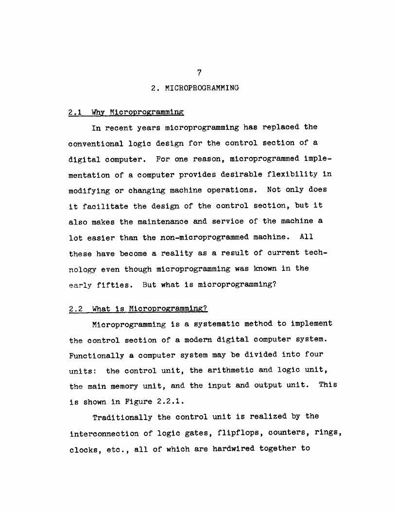
2. MICROPROGRAMMING
2.1 Why Microprogramming
In recent years microprogramming has replaced the
conventional logic design for the control section of a
digital computer. For one reason, microprogrammed imple-
mentation of a computer provides desirable flexibility in
modifying or changing machine operations. Not only does
it facilitate the design of the control section, but it
also makes the maintenance and service of the machine a
lot easier than the non-microprogrammed machine. All
these have become a reality as a result of current tech-
nology even though microprogramming was known in the
early fifties. But what is microprogramming?
2.2 What is Microprogramming?
Microprogramming is a systematic method to implement
the control section of a modern digital computer system.
Functionally a computer system may be divided into four
units: the control unit, the arithmetic and logic unit,
the main memory unit, and the input and output unit. This
is shown in Figure 2.2.1.
Traditionally the control unit is realized by the
interconnection of logic gates, flipflops, counters, rings,
clocks, etc., all of which are hardwired together to
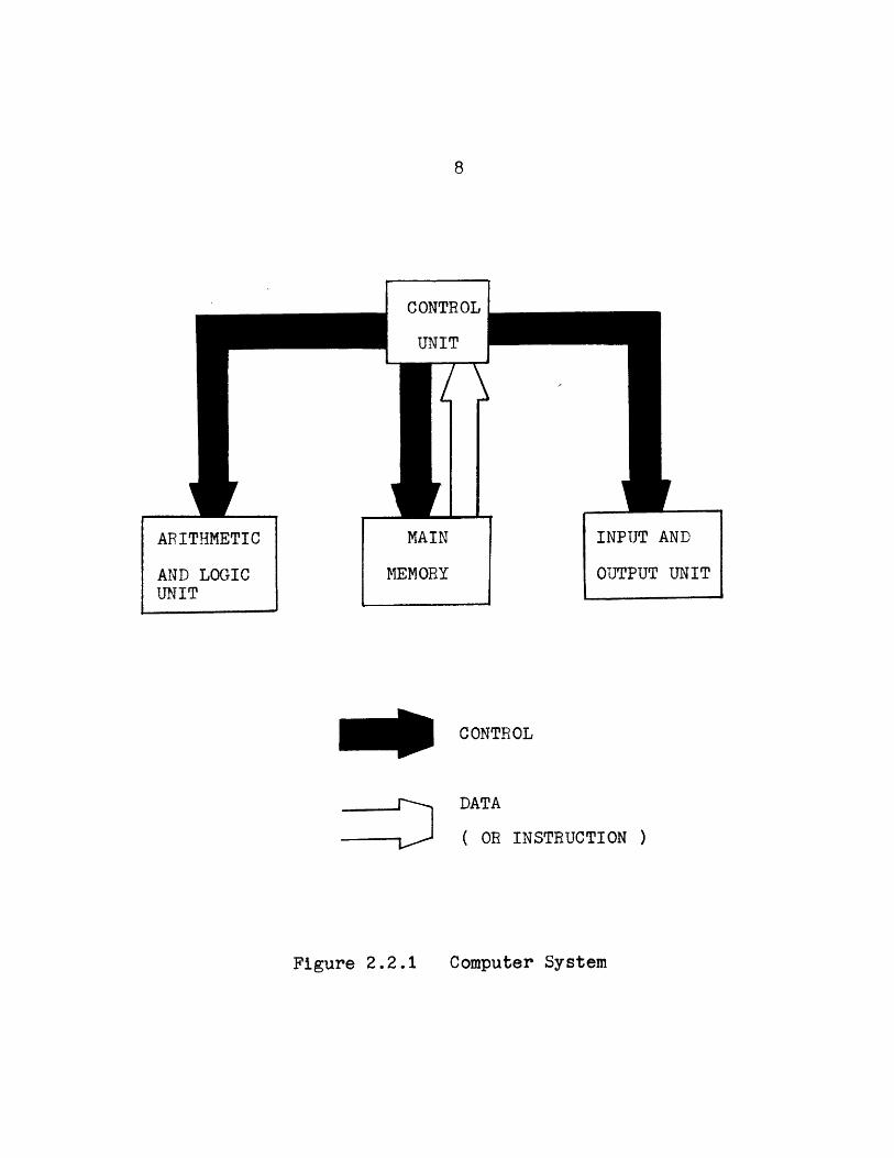
CONTROL
ARITHMETIC
AND LOGICUNIT
INPUT AND
OUTPUT UNIT
CONTROL
DATA
( OR INSTRUCTION )
Figure 2.2.1 Computer System
I
9
generate a sequence of control signals. Should the opera.
tion call for changes, a different sequence of control
signals has to be generated, involving a considerable
reconfiguration of the hardwares. This is inflexible
and ad hoc. In order to provide a more flexible and more
systematic design method than the traditional one, Wilkes
(2) advocated the idea of microprogramming. Here we con-
sider all the sub-machine level operations that are per-
formed to carry out (interpret) the machine operations.
For example a register-to-register addition instructioni
a machine instruction, may be interpreted by the following
sequence of sub-machine level operations:
#1. ADDRESS OF REG 1 TO LOCAL MEMORY ADDRESS REGISTER(LMAR)
#2. TRANSFER CONTENT OF REG 1 TO ADDER INPUT 1
#3. ADDRESS OF REG 2 TO LMAR
#. TRANSFER CONTENT OF REG 2 TO ADDER INPUT 2
#5. SET THE ADDER TO ADD
#6. TRANSFER THE SUM FROM THE ADDER OUTPUT TO THELOCAL MEMORY REGISTER (LMR)
#7. ADDRESS OF REG 1 TO LMAR
#8. WRITE THE CONTENT OF THE LMR INTO THE LOCALMEMORY
Here all the registers are in a fast local memory, see
Figure 2.2.2, which shows a section of a microprocessor
(i.e. a processor that is microprogrammed).1For example a 360 AR instruction
10
#3
42?
OUTPUT
ADDER MODE : ADD, SUBTRACT, ETC.
Figure 2.2.2 A Section of Microprocessor
11
Each of the above basic sub-machine level operation
is known as a micro-operation. Some other examples of
micro-operation are other arithmetic or logical operations
shifting, counting, decrement, increment, register to
register, register to bus transferand main memory request.
Now the designer will gather all the necessary micro-ope-
rations for the machine he is designing. Analogous to a
programmer's preparation of a program, he will formulate
a microprogram to execute all the required machine opera-
tions. The microprogram is a sequence of micro-
instructions each of which may have one or more micro-
operations. Most of the micro-instructions are executed
in one small time period. This is called the processor
cycle time (pc). Some, like a main memory request, may
require two pc's, or three pc's, or more, as present day
main memory speed is still behind the central processor
processing speed. This accounts for the main memory cycle
time (me) of usually two pc's or more. In order to avoid
any waiting for the required data, a fast but costly main
memory may be used. An alternative is to employ a rela-
tively smaller but faster buffer memory in addition to
the slow main memory storage.
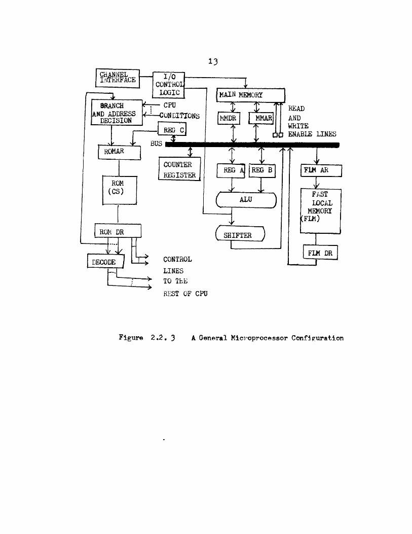
Generally the microprogram is stored in some form of
read-only memory (ROM) as a sequence of ROM words, see
12
Figure 2.2.3. A ROM word format is in Figure 2.2.4 The
ROMAF contains the address of the ROM word to be read out
in ROMDR. The control levels from ROMDR go to the rest
of the CPU to initiate various micro-operations. While
some portion of ROMDR goes to the branch and decision to
set up the next ROM word address, with the help from the
CPU conditions. The ROM and its associated access me-
chanisms is also called the control store unit. Its
cycle time is the control store cycle time (cc). Notice
that there is a high level of parallelism existing in the
microprocessor. If necessary, the adder, the shifter,
the counter, the fast local memory and/or main memory
requests can all be activated at the same time. An illus-
tration is the example 4.1 given in section 4.1.
Also the micro-operations are of very basic primitive
operations. Therefore microprogramming is on a much lower
level than even machine instruction programming. As a
result we can perform a variety of tasks with unusual
speed and efficiency: semaphore manipulation, hardware
special algorithm (like a square root algorithm),emulation,
microdiagnastics, etc. These are some advantages of micro-
programming, others are listed next.
2.3 Advantages of Microprogramming
The advantages of microprogramming are discussed with
13
A General Microprocessor ConfigurationFigure 2.2.- 3
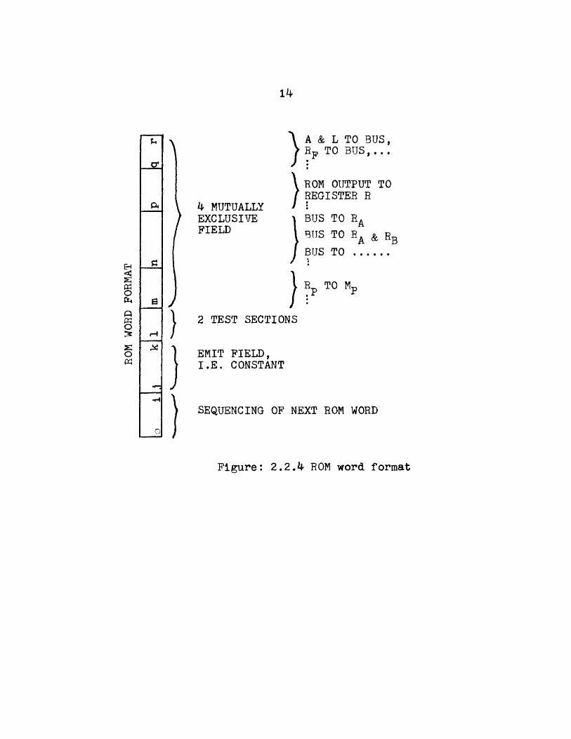
A & L TO BUS,RF TO BUS,...
4 MUTUALLYEXCLUSIVEFIELD
ROM OUTPUTREGISTER R
BUSBUS
BUS
TO
TO RATO RA & RBTO ......
}34
Figure: 2.2.4 ROM word format
H
J P TO M
2 TEST SECTIONS
EMIT FIELD,I.E. CONSTANT
SEQUENCING OF NEXT ROM WORD
15
respect to four view points. First, from a system
architectural view point, the system architecture can be
changed completely, for example by emulation, or extended,
where variable instruction set is allowed. If the machine
instructions were microprogrammed, a large set of instruc-
tions can be implemented for a small system at a low cost.
Second, microprogrammed control makes logic designs sys-
tematic, uniform, and with ease. It is more tractable
to check out the system than the conventional design,
which is hardwired control.
Third, microprogrammed controls takes up very small
space, and it is easy for maintenance. Microdiagnostics
is superior to software diagnostics because of faster
speed and closer resolution. Fourth, microprogramming
is also economical viable after certain point in increa-
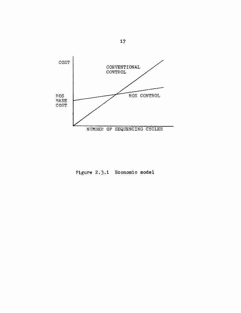
sing logic complexity. An economic model for microprogram-
med logic has set up by Bersner and Mills of IBM (15), and
the conclusion is as follow,
In summary, a crude economic model has been usedto compare the cost of conventional circuits withthe cost of stored logic to perform the same dataprocessing functions. The results indicate thatthere is a point at which, with increasing complex-ity, the cost of stored logic becomes less than thecost of conventional circuits. This cross-overpoint may occur at a relatively low degree of com-plexity. This model can be explored further butthe validity of many of the assumptions and appro-ximations does not warrant anyfurther analysis of it.
16
An intuitive illustration of this model is shown in
Figure 2.3.1.
Disadvantages of Microprogramming
From the architectural and economical views, micro-
grammed control is too expensive to justify for a small
system in which basic repetitive tasks are performed.
As far as performance is concerned, microprogrammed
control may be slow if appropriate overlap between the
control store cycle and the processor cycle is not
established. This overlap issue will be discussed
quantitatively in section 4.2. Finally there is a
hardware cost increase due to ROM and access mechanisms.
2.4. Other meaning of Microprogramming
Microprogramming is also used to denote programming
using machine instructions whose bits are used directly
to control logic gates in the computer. In a sense the
programmer and the logic designer are combined into one.
This term has been used in the Lincoln Laboratory, and
in the work done by Van der Poel (9). Also refer to (10)
for comments on the two types of microprogramming. This
secondary meaning of microprogramming is not oftenly
used. In general the primary meaning of microprogramming
is that of Wilkes, who introduced microprogramming in
the 1950's.
17
CONVENTIONALCONTROL
ROS CONTROL
NUMBER OF SEQUENCING CYCLES
Figure 2.3.1 Economic model
COST
R OSBASECOST
18
2.5 Present Status of Microprogramming
In deed technology played a big role in recognizing
the importance of microprogramming, which was first
noted back in the early 1950's (1), largely credited to
Wilkes (2). For a period of time it remained an idea
and received little attention in both the academic and
industrial worlds. Recently in the 60's, a new interest
has shown (3). This can be seen in the increased number
of articles and technical reports on microprogramming
and on issues closely related to it (3). Text books
begin to mention microprogramming (4,6); some universities
even offer courses on this subject area.
In 1964, IBM announced its System/360, a family of
architecturally compatible computers, that is a program-
mer can write one program for all these computers, because
they are functionally the same to him, even though the
internal hardware configuration of each computer may be
quite different (13). All of the then announced computers
except the largest (model 70) are microprogrammed. This
is followed by the appearance of a number of other systems
that employs this same design philosophy. For example,
the RCA Spectra/70, the Honeywell H 4200/H8200, and
Burroughs 2500 and 3600, Some small microprogrammed com-
puters are Standard Computer Corporation (SCC) IC-model 9,
19
Micro 800, and Meta 4 Series 16 (5). Some of the current
machines with writable control stores are Interdata
Model 3, SCC/C-model 9, and IC-9000, IBM 2025, and IBM
2085.
20
3. A REPRESENTATION SCHEME FOR MICROPROCESSOR
The present trend in computer logic design is that
more and more computers are microprogrammed. Facing
with any two microprocessors, how does one compare them?
This question is not trival unless one is content with
digesting the computer manuals for both microprocessors.
Before going into the microprocessor system, it is pro-
fitable to examine the representation schemes used in
other systems and to see how comparisons are made.
3.1 Review of representation schemes
In this section several system representation schemes
are reviewed. First the system of electrical networks is
examined. In elementary circuit analysis basic building
blocks are resistors, capacitors, inductors, sources, and
some nonlinear devices. A network is then synthesized by
the interconnection of appropriate basic building blocks.
The circuit may be described by differential equations
containing the voltage and current as variables. Given
any two circuits one may examine their topologies and
their differential equation descriptions. Therefore com-
parison may be made between two circuits. In the same
manner it is possible to describe a microprocessor in
terms of circuits. The description, however, may be too
21
detailed for understanding and hence not useful to des-
cribe a microprocessor.
A second possible representation is that of logic
design. Its components are AND, OR, NOT gates. The
system is governed by the properties of the components
and by the laws of boolean algebra. To compare two
logic designs, one merely compares the circuits consisting
of the logic components, or one may compare the boolean
equations. A microprocessor can be represented by this
network of logic components. But even at this level the
description may be still too minute to allow easy compar-
ison of two microprocessors.
A higher level description than logic design is that
of register transfer language (RTL). Currently RTL is
used as a primitive microprogramming language (12). In
this respect RTL is closer to the description of a micro-
processor than the previous two schemes of representation.
Another related scheme of representation is a com-
putational model called the program graphs (16). It can
represent precise description of parallel computations
of arbitrary complexity on nonstructured data. The prog-
ram graph is a directed graph consisted of nodes and
links. While the modes represent computation steps, the
links represent storage and transmission of data and/or
control information. The focus here is on computation,
22
but the hardware structures are relegated to secondary
position of importance. This is rather on contrary to
microprogramming, in which knowledge of the hardware is
essential. Improvement in this respect is included in
another computational model called a computation schema
(11).
A basic computation schema consists of two parts:
the data flow graph, and the precedence graph. The
former represents the data paths in terms of directed
links joining deciders, operators, and cells. Being a
directed graph, the latter prescribes the order of com-
putation in the data flow graph in term of operator,
instance nodes, conditional nodes, and iteration nodes.
The schemata described emphasize the notions of concur-
rency and parallelism. It is powerful in that it can
represent processors of arbitrary complexity. To repre-
sent a computation, one gives its corresponding data flow
graph and precedence graph. In order to represent compu-
tations within a microprocessor, the precedence graph
will be very elaborate and may- challenge the ease of
understanding.
On the other hand there exist macroscopic descrip-
tions of computer systems. The processor-memory switch
(PMS) and the instruction-set processor (ISP) are two new
language developed by Bell and Newell to describe
23
computer systems (6). The PMS represents major hardware
units in a processor. Its basic components are the pro-
cessor, memory, switch, and control unit. At the ISP level
a processor is described completely by giving the instruc-
tion set and the interpreter of the processor. The inter-
preter is in terms of its operations, data-types, and mem-
ories. As the-name as well as the language indicates,
both PMS and ISP are too macroscopic to describe the mi-
croprocessor. For example, the processor, and control
units are basic components in the PMS description. How-
ever, the interest here is to know more about the processor
and the control units themselves, not as unit components,
but as systems themselves.
3.2 A representation scheme for microprocessor
The previous representation schemes are adequate in
their own domain of description. As far as representing
microprocessor is concerned they are inadequate. Either
the representation scheme is too detailed and thus becomes
too complicated; or too restricted, as in the program
graphs and computation schemata; or too macroscopic, as
in the PMS and ISP. In the case of microprocessor the
focus is on its general characteristics which involves
issues like the following: flexibility of data path, how
many buses it has, how many working register it has, what
24
are the data transfer restrictions, what are the timing
relationships, etc.
With the needs mentioned above, a representation
scheme is proposed here to represent a microprocessor.
The scheme has three components: the structure represen-
tation, the transfer constraint, and the cycle time.
First the structure representation component is presented.
It conveys the general hardware structure of the micro-
processor. The general hardware structure refers to the
conventional central processor hardwares, which includes
the arithmetic and logic unit, with the working registers,
the high speed local memory, and the control unit - ROM
and associated hardware mechanisms. Also, buffer (or
cache) memory unit, main memory unit, and input output un-
it are represented. Besides representing the general
hardware structure, the structure representation also
indicates the general data flows within the microprocessor.
This realization is to be done with the minimum amount of
complexity shown in the representation.
The general hardware structure of a microprocessor
is abstractly represented by a set of passive and active
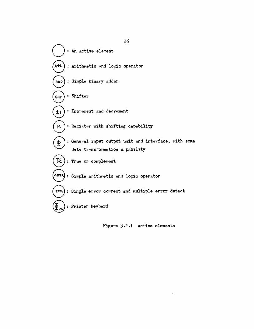
elements. Active elements represent hardware units that
performs transformations on data, and in general are
denoted by , or Q . While the former represents
25
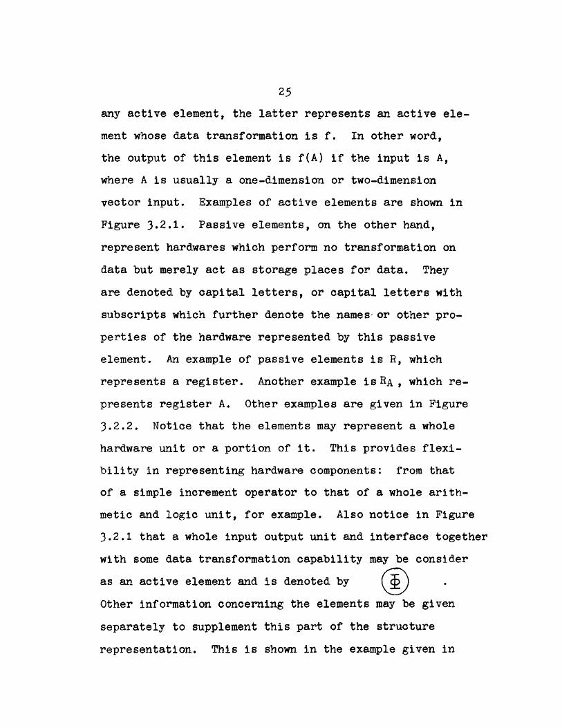
any active element, the latter represents an active ele-
ment whose data transformation is f. In other word,
the output of this element is f(A) if the input is A,
where A is usually a one-dimension or two-dimension
vector input. Examples of active elements are shown in
Figure 3.2.1. Passive elements, on the other hand,
represent hardwares which perform no transformation on
data but merely act as storage places for data. They
are denoted by capital letters, or capital letters with
subscripts which further denote the names- or other pro-
perties of the hardware represented by this passive
element. An example of passive elements is R, which
represents a register. Another example is RA, which re-
presents register A. Other examples are given in Figure
3.2.2. Notice that the elements may represent a whole
hardware unit or a portion of it. This provides flexi-
bility in representing hardware components: from that
of a simple increment operator to that of a whole arith-
metic and logic unit, for example. Also notice in Figure
3.2.1 that a whole input output unit and interface together
with some data transformation capability may be consider
as an active element and is denoted by
Other information concerning the elements may be given
separately to supplement this part of the structure
representation. This is shown in the example given in
26
An active element
Arithmetic ind logic operator
Simple binary adder
Shifter
Increment and decrement
Register with shifting capability
General input output unit and interface, with some
data transformation capability
True or complement
Sirple arithnetic and logic operator
Single error correct and multiple error detect
Printer keybard
Figure 3.?.1 Active elements
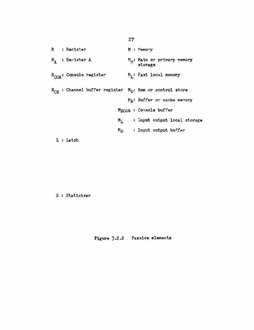
R : Resister
RA Register A
27
M :
ML:RCON: Console register
RcB : Channel buffer register M U:
MB:
M BCON
ML
MB :
Memory
Main or primary memorystorage
Fast local memory
Rom or control store
Buffer or cache memory
Console buffer
Input output local storage
Input output buffer
L : Latch
S : Staticizer
Figure 3.2.2 Passive elements
28
section 3.3.
To indicate the general data flows within the
microprocessor, a set of links is used to connect
graphically all the passive and active elements which
represent the hardware structure of the microprocessor.
This set includes the following three links:
2.
3.
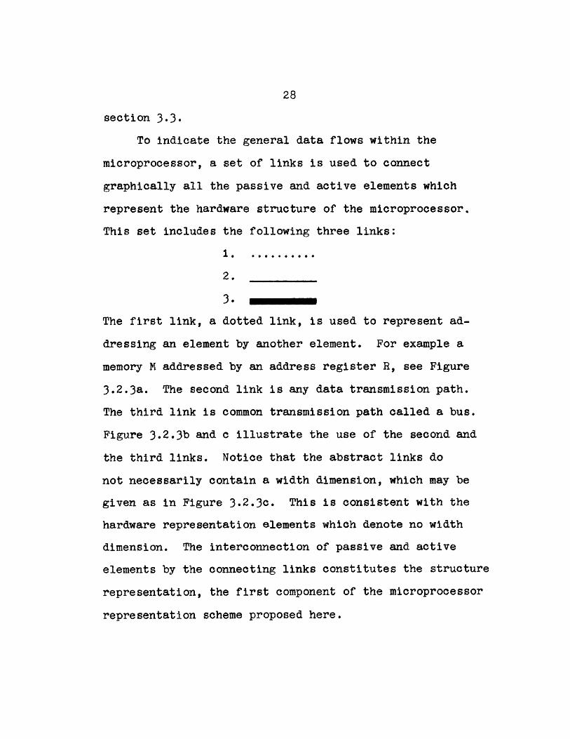
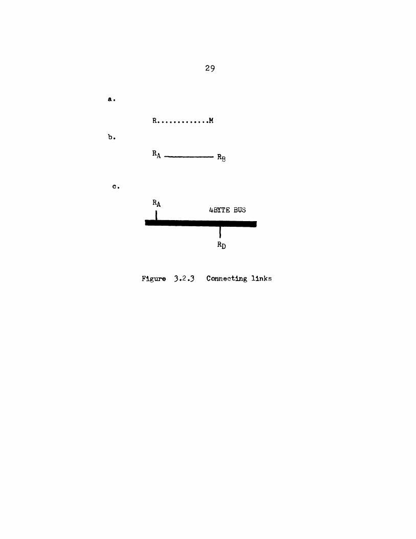
The first link, a dotted link, is used to represent ad-
dressing an element by another element. For example a
memory M addressed by an address register R, see Figure
3.2.3a. The second link is any data transmission path.
The third link is common transmission path called a bus.
Figure 3.2.3b and c illustrate the use of the second and
the third links. Notice that the abstract links do
not necessarily contain a width dimension, which may be
given as in Figure 3.2.3c. This is consistent with the
hardware representation elements which denote no width
dimension. The interconnection of passive and active
elements by the connecting links constitutes the structure
representation, the first component of the microprocessor
representation scheme proposed here.
29
R. ........ M
RA RB
4BYTE BUS
Figure 3.2.3 Connecting links
30
The transfer constraint
The second component of the microprocessor represen-
ration scheme is called the transfer constraint. This
component can reveal all the detailed data flows and
hardware structures within the microprocessor. It exhi-
bits the nature of the micro-operations defined in conjunc-
tion with this microprocessor. If the micro-operations
are simple and basic, microprogramming is easy and may
have flexible implementation of machine instructions.
If they are highly specialized, microprogramming may be
difficult. Also what matters most in a microprocessor is
the micro-operations that are allowed. All these informa-
tion is contained in the ROM word format. Therefore the
transfer constraint is denoted by the format of a ROM
word together with explanation of all the fields of the
ROM word. Consequently the transfer constraint conveys
more information than that mentioned before.
In addition, the transfer constraint tells the
sequencing of ROM words. It shows the emit field, that
is the constant field, and its size. As far as the micro-
operations are concerned, the transfer constraint lists
the mutually exclusive micro-operations defined by the
hardwares and by the designers of the microprocessor.
An example of the transfer constraint is shown in section
3.3. The transfer constraint, together with the structure,
31
is still not complete. It requires the third component
as well to complete the representation scheme.
The cycle time
Even though the transfer constraint conveys a vast
amount of information, it has no notion of any timing
relationship whatsoever. For example, a certain combin-
ation of bits in a field of the ROM word is for making
main memory read operation. This does not tell how long
it will take to get the data from the main memory.
It is true in a microprocessor that most hardware
operations are of time durations equal or less than the
processor cycle time. In these cases, knowledge of the
timings may not be necessary. In a main memory request,
it is necessary to know how long it takes to get the data
so that other operations may be performed on it. Usually
the main memory is slower than the CPU processing speed.
Similarly is the case for the local memory store. Its
cycle time is critical for application of some micro-
operations. The main memory and local memory cycle times
are not the determining factors for the system performance.
Partly the performance depends on the processor cycle time.
It is obvious that if two processors are identical except
for the processor cycle time then their relative perform-
ance is determined by their relative processor cycle time.
32
Finally the control store cycle time also determine the
performance.
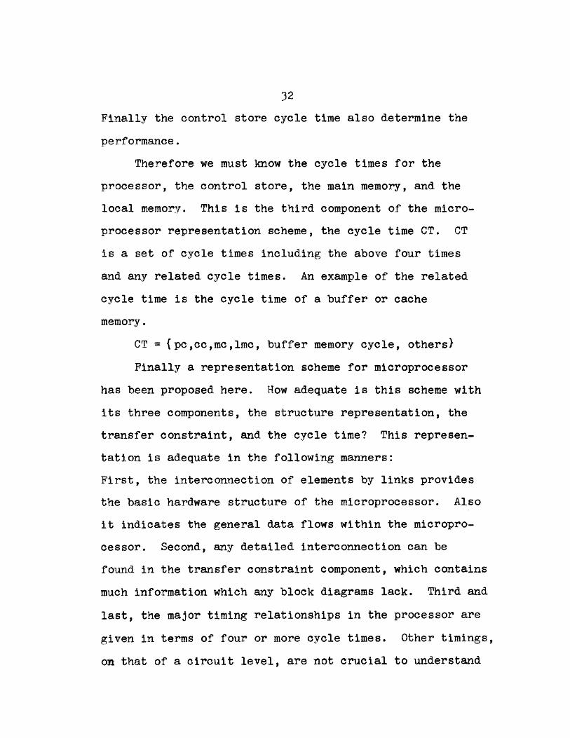
Therefore we must know the cycle times for the
processor, the control store, the main memory, and the
local memory. This is the third component of the micro-
processor representation scheme, the cycle time CT. CT
is a set of cycle times including the above four times
and any related cycle times. An example of the related
cycle time is the cycle time of a buffer or cache
memory.
CT = {pc,ccmclmc, buffer memory cycle, others)
Finally a representation scheme for microprocessor
has been proposed here. How adequate is this scheme with
its three components, the structure representation, the
transfer constraint, and the cycle time? This represen-
tation is adequate in the following manners:
First, the interconnection of elements by links provides
the basic hardware structure of the microprocessor. Also
it indicates the general data flows within the micropro-
cessor. Second, any detailed interconnection can be
found in the transfer constraint component, which contains
much information which any block diagrams lack. Third and
last, the major timing relationships in the processor are
given in terms of four or more cycle times. Other timings,
on that of a circuit level, are not crucial to understand
33
the system structures and the general data flows.
To illustrate the representation scheme, an example
is given next.
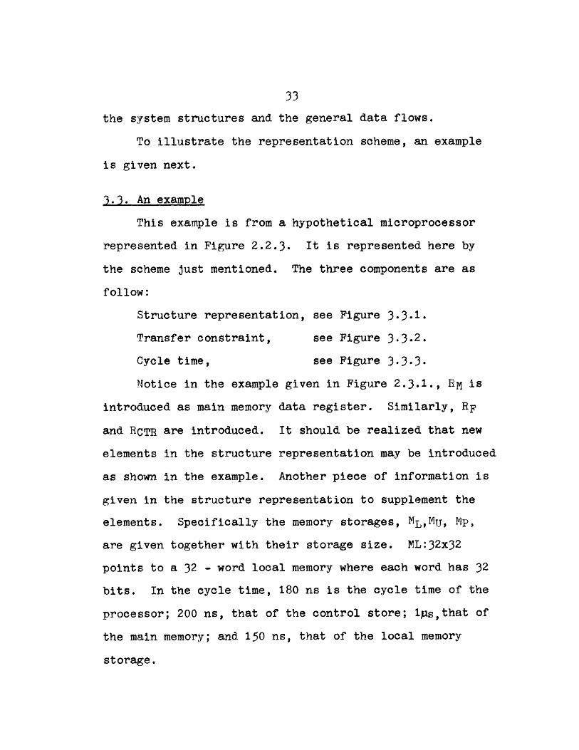
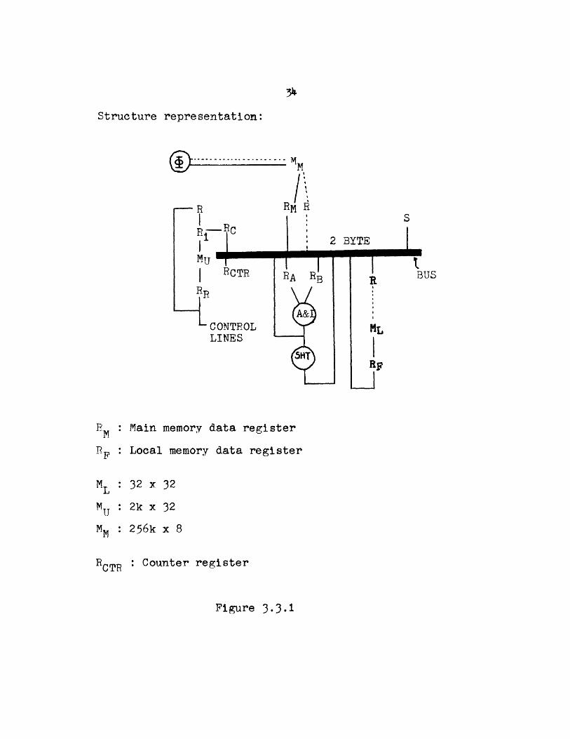
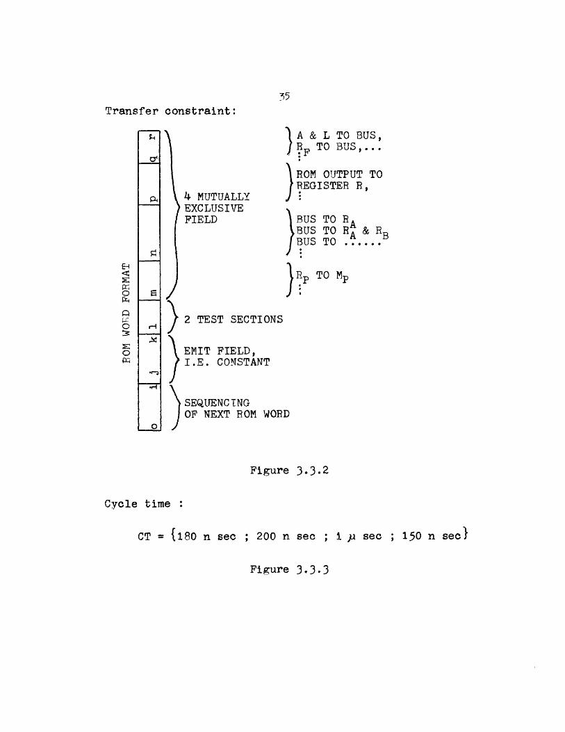
3.3. An example
This example is from a hypothetical microprocessor
represented in Figure 2.2.3. It is represented here by
the scheme just mentioned. The three components are as
follow:
Structure representation, see Figure 3.3.1.
Transfer constraint, see Figure 3.3.2.
Cycle time, see Figure 3.3.3.
Notice in the example given in Figure 2.3.1., EM is
introduced as main memory data register. Similarly, RF
and RCTR are introduced. It should be realized that new
elements in the structure representation may be introduced
as shown in the example. Another piece of information is
given in the structure representation to supplement the
elements. Specifically the memory storages, MLMU, Np,
are given together with their storage size. ML:32x32
points to a 32 - word local memory where each word has 32
bits. In the cycle time, 180 ns is the cycle time of the
processor; 200 ns, that of the control store; 1ps,that of
the main memory; and 150 ns, that of the local memory
storage.
Structure representation:
RC
MURCTR BA
RB
A&CONTROLLINES
2 BYTE
: Main memory data register
: Local memory data register
: 32 x 32
: 2k x 32
: 256k x 8
R : Counter register
Figure 3.3.1
ML
BUS
RMP
ML
MU
RCT
Transfer constraint:
4 MUTUALLYEXCLUSIVEFIELD
2 TEST SECTIO
EMIT FIELD,I.E. CONSTANT
SEQUENC INGOF NEXT ROM W
A & L TO BUS,F TO BUS,...
ROM OUTPUT TOREGISTER R,
BUS TOBUS TOBUS TO
R p TO I
RARA & RB...... *
ORD
Figure 3.3.2
Cycle time :
CT = i180 n sec ; 200 n sec ; I p sec ; 150 n sec 1
Figure 3.3.3
H
0
NS
36
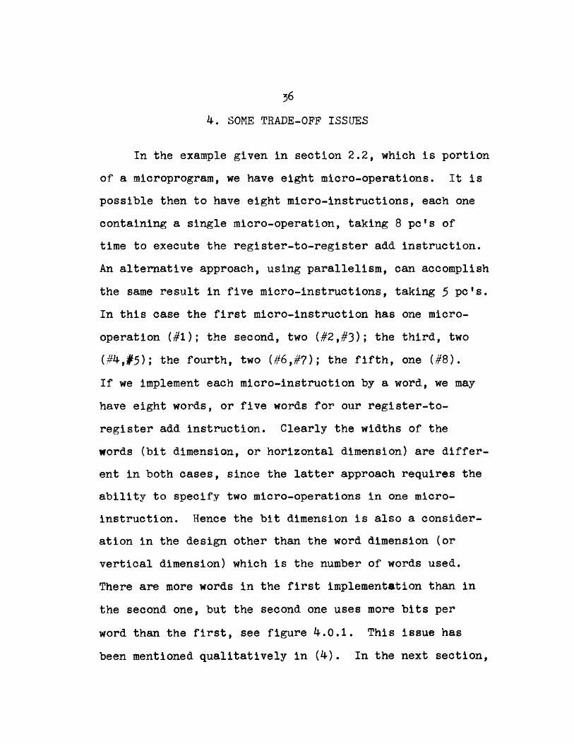
4. SOME TRADE-OFF ISSUES
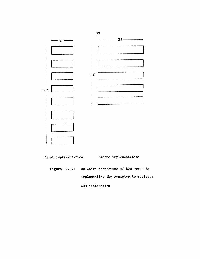
In the example given in section 2.2, which is portion
of a microprogram, we have eight micro-operations. It is
possible then to have eight micro-instructions, each one
containing a single micro-operation, taking 8 pc's of
time to execute the register-to-register add instruction.
An alternative approach, using parallelism, can accomplish
the same result in five micro-instructions, taking 5 pc's.
In this case the first micro-instruction has one micro-
operation (#1); the second, two (#2,#3); the third, two
(14,#5); the fourth, two (#6,#7); the fifth, one (#8).
If we implement each micro-instruction by a word, we may
have eight words, or five words for our register-to-
register add instruction. Clearly the widths of the
words (bit dimension, or horizontal dimension) are differ-
ent in both cases, since the latter approach requires the
ability to specify two micro-operations in one micro-
instruction. Hence the bit dimension is also a consider-
ation in the design other than the word dimension (or
vertical dimension) which is the number of words used.
There are more words in the first implementation than in
the second one, but the second one uses more bits per
word than the first, see figure 4.0.1. This issue has
been mentioned qualitatively in (4). In the next section,
4-
First implementation
372X
5Y
LKLEl
zuliliiJI7
Second implfementption
Figure 4.0.1 Relntive dimensions of ROM vordis in
implementing the rpgistpr-to..register
add instruction
38a quantitative analysis of this trade-off is given. Two
other trade-off issues are covered in sections 4.2 and
4.3.
4.1 Horizontal and vertical dimensions of ROM words
As the above example has shown,one of the design
issues is to determine the width of the ROM word and
the number of ROM words. If the horizontal dimension
is increased, the performance is improved because fewer
words are needed to implement a particular instruction.
However, increase in width invokes high cost as a result
of memory increase,ROM data register bits increase, access
mechanisms increase. On the other hand a decrease in
width implies an increase in the number of ROM words used.
Cost is reduced because more ROM words only calls for
cost in memory; no access mechanisms are involved. Now
the performance is degraded as more words are needed to
implement the instruction. The trade-off problem here
is to choose the optimum horizontal and vertical dimensions
for lowest cost and at the same time meets the performance
requirement.
To formulate this trade-off problem in precise terms,
the following assumptions and definitions are taken:
A set of micro-operations, (... mi...) is established
as the most primitive hardware operations in the micro-
processor. Each machine instruction i is to be implemented
39
by choosing micro-operations from the set. A particular
machine instruction may consist of following sequence:
ml, m2, m3;*
m6, m9, m1 0 , m13
m7, m 8, m1, mi15 , m16, m4, m5 , mig, m20;
m 3 0, m3l, m32, m 3 7 , m50-
The above sequence may be executed in at least four con-
secutive instances of times (steps). Each step performs
different number of micro-operations; three in the first
step, four in second step, nine in the third, and five
in the fourth. This sequence of steps is abbreviated as
(3, 4*, 9, 5)
or in general,*
tnij, ni2, ng,., nig,...}
for a particular machine instruction i which can perform
as many as nil micro-operations simultaneously in the first
step, as many as ni2 in the second step, and so on. The
execution order of the steps as given must be kept, as
results in a previous step may be needed by micro-operations
in the current step. nij indicates branching is to be per-
formed.
The total cost of the ROM and its associated access
mechanisms is no more than C, the cost constraint.
There is a speed requirement, Si, for each machine
instruction. Machine instructions include basic machine
40
instructions like binary, decimal, floating point, logical
instructions, and system instructions like V operation,
or P operation. Also there is no sharing of ROM words
among machine instructions.
Let T be the processor cycle time. As the width of
the ROM increases, T has a slight increase because word
drive pulse has to propagate a longer path. For this
analysis T is assumed to be constant over the range of
x that is of interest.
Let a be the cost per bit for ROM word access
mechanism and its associated hardware and design cost.
Hardwares here include ROM data register, ROM field deco-
des and drivers, and sense amplifiers.
Let g(k) be the cost per word for a word of k bits.
Here g(k) involves just memory cost and therefore is
much smaller than a k. Then g(k) = k b, where b is the
cost of memory per bit.
Finally let
x be the number of bits per word
yi be the number of words for machine instruction i.
y be the total number of words for all machine instruc-
tions.
Then the first trade-off issue can be formulated as
Minimize f = xa + y x b
41
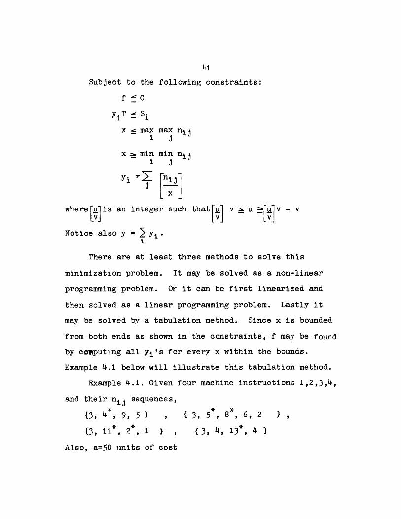
Subject to the following constraints:
f C
y.T Si
x 5 max max niji j
x min min nii j
Yi IInii]x
where2lis an integer such that v _ u - v
Notice also y = y.
There are at least three methods to solve this
minimization problem. It may be solved as a non-linear
programming problem. Or it can be first linearized and
then solved as a linear programming problem. Lastly it
may be solved by a tabulation method. Since x is bounded
from both ends as shown in the constraints, f may be found
by computing all yi's for every x within the bounds.
Example 4.1 below will illustrate this tabulation method.
Example 4.1. Given four machine instructions 1,2,3,4,
and their njj sequences,
{3, 4*,9,5 , { 3, 5, 8*, 6,2 ,
{3, 11*, 2*, 1 ) ,( 3, 4, 13*, 4 )
Also, a=50 units of cost
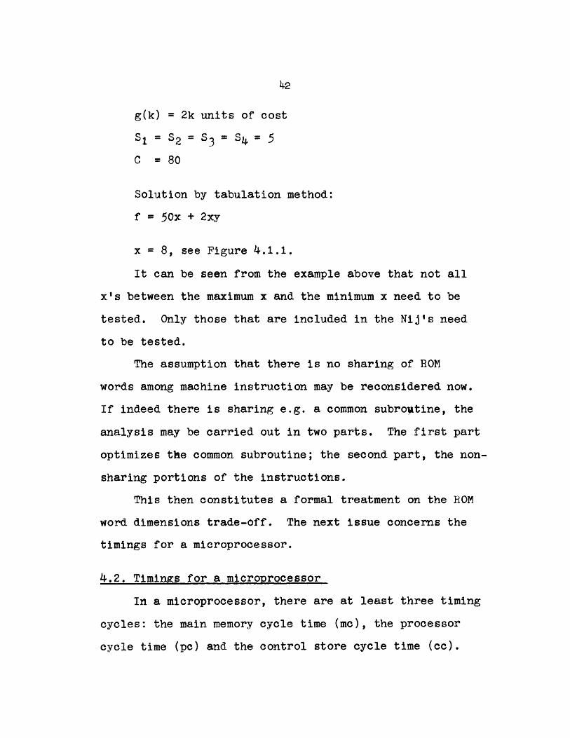
g(k) = 2k units of cost
S1 = S2 S S3 = S4 = 5
C = 80
Solution by tabulation method:
f = 50x + 2xy
x = 8, see Figure 4.1.1.
It can be seen from the example above that not all
x's between the maximum x and the minimum x need to be
tested. Only those that are included in the Nij's need
to be tested.
The assumption that there is no sharing of ROM
words among machine instruction may be reconsidered now.
If indeed there is sharing e.g. a common subroutine, the
analysis may be carried out in two parts. The first part
optimizes the common subroutine; the second part, the non-
sharing portions of the instructions.
This then constitutes a formal treatment on the ROM
word dimensions trade-off. The next issue concerns the
timings for a microprocessor.
4.2. Timings for a microprocessor
In a microprocessor, there are at least three timing
cycles: the main memory cycle time (mc), the processor
cycle time (pe) and the control store cycle time (cc).
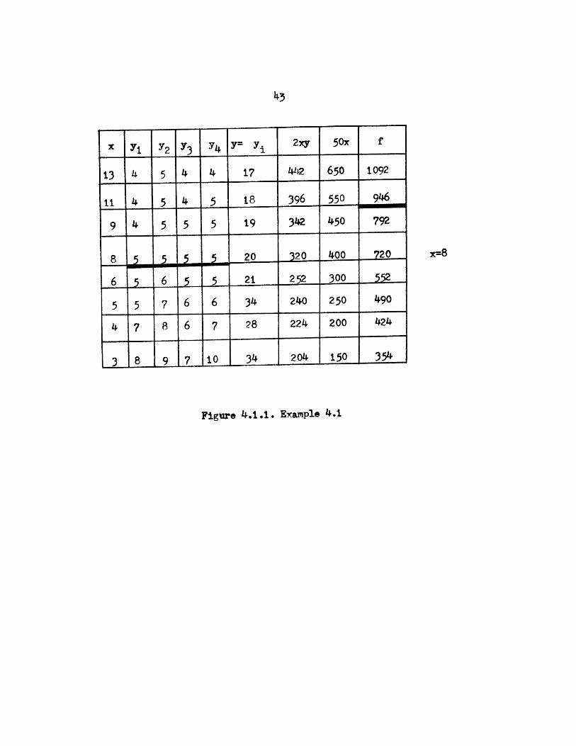
x y1 1 2 Y3 Y4 yy 2xy 50x f
13 4 5 4 4 17 442 650 1092
11 4 5 4 5 18 396 550 946
9 4 5 5 5 19 342 450 792
8 5 5 5 5 20 320o 400 720
6 5 6 5 5.. 21 252 300 55
5 5 7-6 6 34 240 250 490
8 6
9-
28 224 200 424
204 150 354, , .- , I______
Figure 4.1.1. Example 4.1
4
3
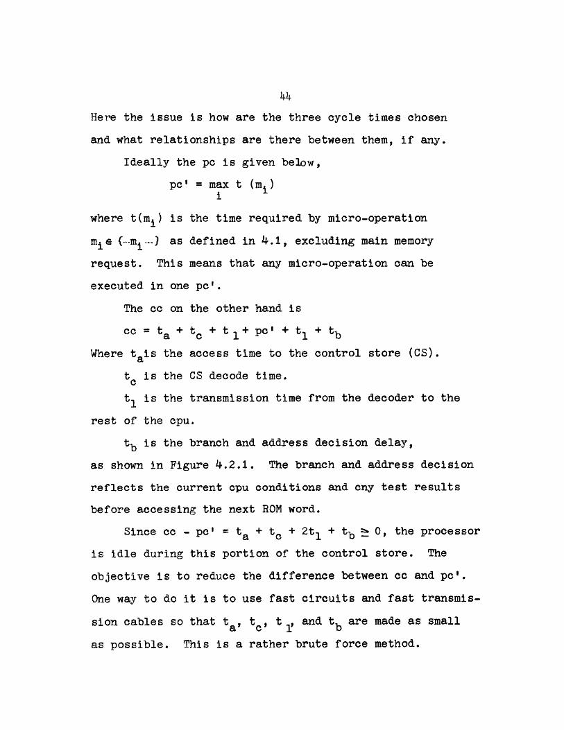
Here the issue is how are the three cycle times chosen
and what relationships are there between them, if any.
Ideally the pc is given below,
pc' = max t (m )i
where t(mi) is the time required by micro-operation
mie {-m.-) as defined in 4.1, excluding main memory
request. This means that any micro-operation can be
executed in one pc'.
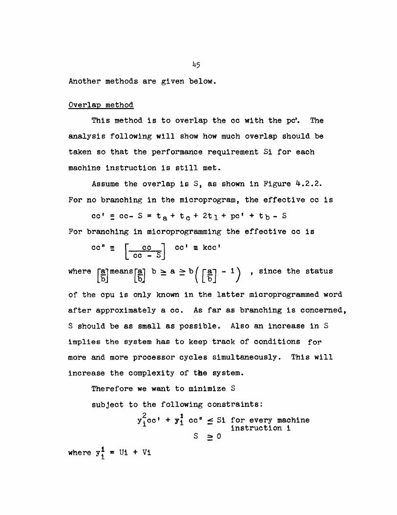
The cc on the other hand is
cc = ta + to + t 1 + pc' + t1 + tb
Where tais the access time to the control store (CS).
tc is the CS decode time.
t is the transmission time from the decoder to the
rest of the cpu.
tb is the branch and address decision delay,
as shown in Figure 4.2.1. The branch and address decision
reflects the current opu conditions and cny test results
before accessing the next ROM word.
Since c - pc' = ta + t + 2t + tb ' 0, the processor
is idle during this portion of the control store. The
objective is to reduce the difference between cc and pc'.
One way to do it is to use fast circuits and fast transmis-
sion cables so that ta' IC t 1, and tb are made as small
as possible. This is a rather brute force method.
145
Another methods are given below.
Overlap method
This method is to overlap the cc with the pc'. The
analysis following will show how much overlap should be
taken so that the performance requirement Si for each
machine instruction is still met.
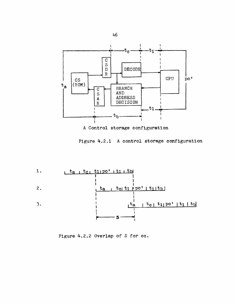
Assume the overlap is S, as shown in Figure 4.2.2.
For no branching in the microprogram, the effective cc is
cc' = cc- S = ta+ tc+ 2ti+ pc' + tb - S
For branching in microprogramming the effective cc is
cc" [ cc cc' a kcc'cc - S]
where [ajm eansraJ b a e b([ 1 ,since the status
of the cpu is only known in the latter microprogrammed word
after approximately a cc. As far as branching is concerned,
S should be as small as possible. Also an increase in S
implies the system has to keep track of conditions for
more and more processor cycles simultaneously. This will
increase the complexity of the system.
Therefore we want to minimize S
subject to the following constraints:
y2c' + yi cc" g Si for every machineinstruction i
S w=i0
where yl = Ui + Vi
I t tOij
rnC
tb
A Control storage configuration
Figure 4.2.1 A control storage configuration
i ta tc tipc' i t1 i tbII I
,ta t I_ tilpO' Iti I-tbl
|- S -ba
Figure 4.2.2 Overlap of S for cc.
ta i tcl tl1 pPC' I t1-ilth.
Ui = number of nj* in Yj
Vi = 1,if last n is n , or if last nij is not
the k th item in the last k grouping of nj 's.(See Multiple access for groupings of ni .)
,0,otherwise
y = number of n 's not included in yI iiand there must be no overlap between same t,' s from
different ROM cycles, tie ( ta, tc' tl, pc', tb )
This can be solved as a linear programming problem to get
the optimum value of S. Or it may be solved by taking
value of k from 1 to n, for some n, and list the cons-
traints for each k to get the optimum S.
Now the effective pc = cc' = cc - S, while-the
control store cycle time still is cc.
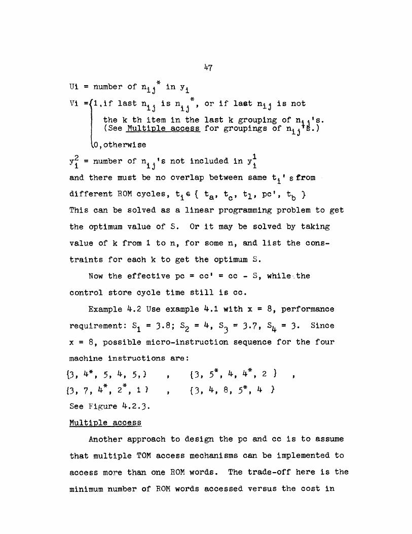
Example 4.2 Use example 4.1 with x = 8, performance
requirement: S, = 3.8; S2 = ' S3 = 3.7, S4 = 3. Since
x = 8, possible micro-instruction sequence for the four
machine instructions are:
{3, 4*, 5, 4, 5,) , 3, 5*, 4, 4*, 2 ,
{3, 7, 4*, 2*, 1 ) , {3, 4, 8, 5*, 4 )
See Figure 4.2.3.
Multiple access
Another approach to design the pc and cc is to assume
that multiple TOM access mechanisms can be implemented to
access more than one ROM words. The trade-off here is the
minimum number of ROM words accessed versus the cost in
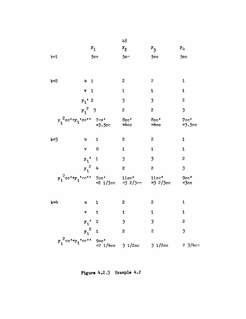
5cc
u1
vi
Yj' 2
yi 2 3
y 2cc'+y 'cc'' 7
U 1
v 0
y ' 1
3.5cc
7.2 41
y 2cc'+y 'ec'' 7
. u 1
v 1
71'
yi2
y. cc'+y 'cc''
cc' 11cc' 11cc'2 1/3cc =3 2/3cc =3 2/3cc
9cc'=2 1/4cc 3 1/2cc
2
1
3
2
3 1/2cc
Figure 4.2.3 Example 4.2
k=1
k=2
48
Y2
Sc-
2
1
3
2
y 3
5cc
2
1
3
8cc'=4cc
y4
5cc
1
1
2
3
7cc'=3.5cc
8cc'=4cc
9cc'=3cc
2 3/4cc
k=3
k=5
'Ii
y 2
j 2ce'+yi'ce
1
2
1
2 1/5cc
Y4
2
3
3 2/5cc 3 2/5cc 2 3/5cc
. . k3 is optimum
PC = cc' = cc - S = . =.cc
k 3
Figure 4.2.3 Example 4.2 (cont.)
50
the number of access mechanisms used.
let w be the number of ROM words accessed at one
time. It is desired to
Minimize w
Subject to the following constraints:
g cc1 (w) <_ Si Vmachine instruction i
w Ca <CA
where cc1 (w) = cc + (w -1) pC'
Ca is the approximate cost of the access mechanisms
for a single ROM word.
CA is the total cost allowed for access mechanisms
Given a sequence of micro-instructions nij ferig
machine instruction i, grouping of nij is by k
starting with lowest j. Each grouping either
has k or less n13 's. For the latter case the
last nij must be a nij or it is not the k th
item in the last k grouping of nij's. Let
gk be the number of such groupings. g = k=w
Therefore the optimum w will give the optimum cc1 (w)
= cc + (w-1) PC'.
Now the speed gain is clear because w pc"s are sharing
one (cc - pc') instead of 1 pc' sharing one (cc - pc') in
a single ROM access strategy.
Example 4.3 Given 4 machine instructions with n 's
as follow:
(3,4*,9,5) {3,5* ,8*,2 ) ,(3,11*,2*,1 },
(3,4,13*,4)
x = 8, performance requirement: S1 = 3.8, 32 = 4,
S3 = 5, S4 = 6;
CA = 3Ca. Finally, pc' = 1/3(cc - pC'), or pc' = cc.
Solution by tabulation method : See Figure 4.2.4.
The underlines indicate the grouping of multiple access.
In the above example the optimum solution is w=2.
It is important to realize that the performance Si
may be relaxed so that only certain desired machine
instructions have the performance constraints Si's, as
long as the total performance is under certain limit,
that is ygT -<Si for ie { desired machine ins-truction i )
y, T !Sii i
are used instead of the stricter constraints of
y T I Si machine instruction i.
So far the discussion involves only pc and cc. Now
me will be considered. There is really no basic depen-
dence between me and pc, or between mc and cc. However,
it is desirable to have mc = pc so that there is no waiting
when data is required. If mc = 2pc's or more, there is a
performance loss of 1 pc or more everywhere there is a
main memory request and that this can not be moved earlier
by 1 pc or more ( or equivalently by 1 ROM word or more).
Since x=8, possible Nij sequences are as follow:
3,4*, 5,4,5 3,5 *,4,4 *,2 3,7,4* ,2*,1 3,4,8,5*,4
w=1 5cc1 (1)
w=2 1,4t*,._4,5-
3cci(2)
=3 3/4 cc,(I)3cct(2)= 3 3/4 cc(1)
4cc1 (2)=5cc1 (1)
3ccj(2)=3 3/4ccl(1)
w=3 , 5.4.5
2CC0(3)
=4 1/4cc(1) =4 1/4ccl(1) =4 1/4cci(1)
Figure 4.2.4 Example 4.3
5cc (1) 5cc(I) 5cci(1)
3cc (3 )
j3cc1 (1)
3cci(3) 3ccl(3)
O,4$*,t 3.7.49 *, less 3.4.8,6e 4..
53
Hence there is strong dependence between pc and cc
but little or no dependence of either one with mc. The
next issue on trade-offs is on how much encoding.
4.3 Encoding of ROM bits
Finally we will deal with the encoding problem for
the ROM fields. Encoding saves bits and hence cost,
but it increases control line delay time because it
requires time to decode.
The assumptions are the following:
. A group of mutually exclusive lines are to be encoded
(n).
. If a line is not encoded, its cost is Cw.
If a line is one of j encoded lines, its cost is
(log2j) Cw.
The cost of decoding is offset by the saving resulting
from the reduction of ROM bits.
A cost limit Co is imposed, and (log2n) Cw/n f Co <nCw
. Decoding delay is approximately linear with the number
of lines encoded, i.e.
Atj jT0
where tj is the j - out put decoder delay; T0 is a
very small number.
. Associated with each line is ti and Ti, where ti is
the delay time of line i without encoding. Ti is the
maximum delay for line i whether it is encoded or not.
The problem of encoding M lines out of n lines is to
maximize M
subject to the following constraints:
ti + 4tM e Ti V line i that is encoded
(n - M) Cw + (log2 M) Cw/M<Co
M = , where k is an nonnegative integer.
Example 4.4 Encoding problem for group of 8
mutually exclusive control lines. The following infor-
mation is given:
Cw = 10; Co = 60; t1 = 7, t2 = 6, t3 = 8, t4 = 9,t5 = 4,
t6 = 6, t7 = 7, t8 = 6; T1= 10, T2 = 9, T3 = 10, T4 = 15,
T5 = 10, T6 = 9, T7 = 14, T8 = 13
Maximize M
subject to ti + tM = ti + M < Ti
(8 - M) 10 + (log2M) 10/M < 60
M =2k
Solution by tabulation: See figure 4.3.1.
For M = 2, 60 + }-10 = 65 $ 60
4, 40 + -10 = 45 < 60
8, 80 $60
M = 4 on lines 4, 5, 7, 8
X marks indicates that a line may be encoded
for a particular M.
t.
1 7
2 6
3 8
4 9
5 4
6 6
7 7
8 6
Figure 4.3.1 Example 4.4
M=8M=2
xx
x
x
x
x
X
x
T i
10
8
9
15
10
9
11
12
5. SUMMARIES OF MICEOPROCESSORS
The summaries of microprocessors are given here in
term of the representation scheme developed in chapter 3.
Each microprocessor is summarized in three components:
1) the structure representation, 2) the transfer cons-
traint, and 3) the cycle time. This serves to illustrate
the representation scheme as used on some major micro-
programmed computers. Another purpose is for ready com-
parison of microprocessors. The machines given below
include the ones from Honeywell, IBM, RCA, and Univac:
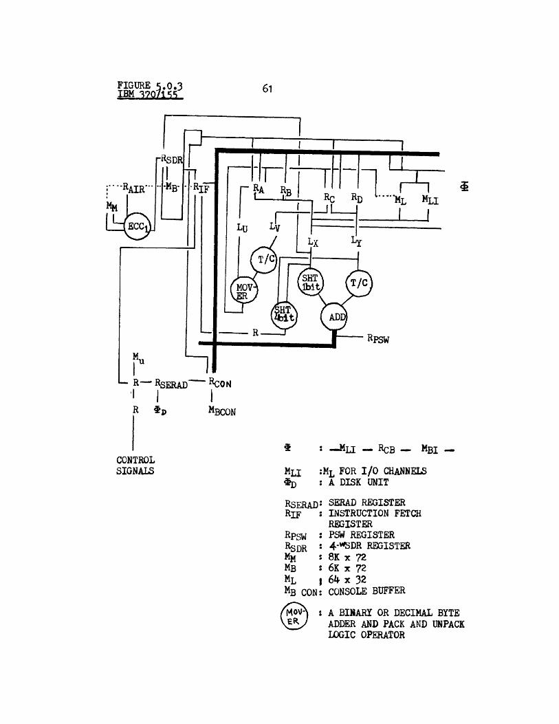
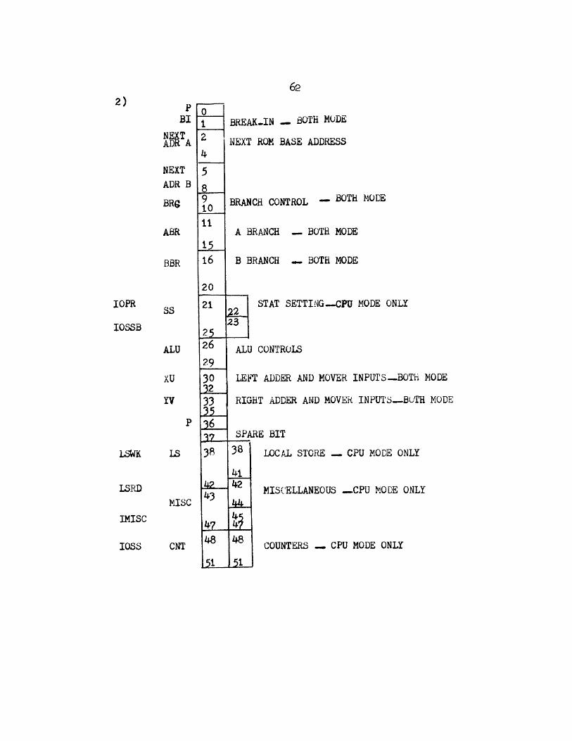
H4200 : Medium-to-large business data processing.
Figure 5.0.1.
IBM 360/40 : Medium-to-small general purpose process-
ing. Figure 5.0.2.IBM 370/155 : Medium high performance general purpose
processing. Figure 5.0.3.
RCA SPECTRA/70: Medium general purpose processing.
Figure 5.0.4.
UNIVAC C/SP: Medium communication processing.
Figure 5.0.5.
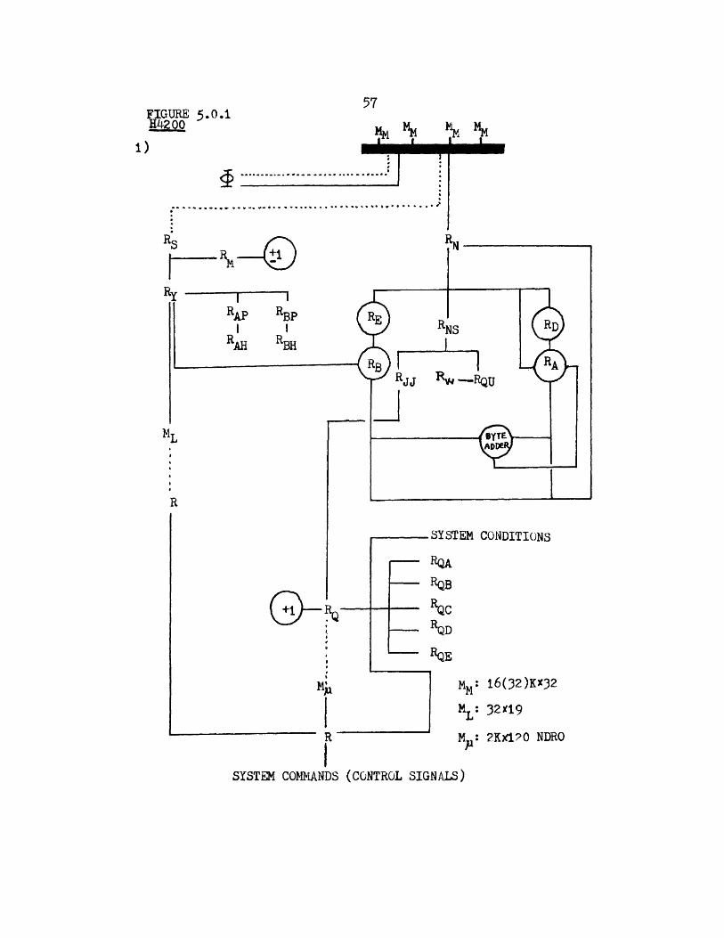
FIGURE 5.0.1H4200
mN1 1
-'IS
RAp RBPI I
R~ RBH
Rjj -RKQU
SYSTEM CONDITIONS
RQA
RQB
RQC
"QD- RQE
M
R M
SYSTEM COMMANDS (CONTROL SIGNALS)
M:
L:
:
16(32)Kx32
32X19
2Kx1?0 NDRO
0-
2) bit1 ~ NEXT f PARITY FOR BRANCH ADDRESS FIELD2 ~ DROM ' BRANCH ADDRESS FIELD FOR RQA -RQF
ADDRESS
1213 ~ C BRANCH ON STORED TEST14 ~ SELECT ONE OF FOUR GROUPS OF SEVEN15 L TEST ACTIONS IN EACH TEST SECTION16 EACH FIELD [QUAD GATE SELECT A18 SELECTS WHICH L19 SEVEN TESTS QUAD GATE SELECT B
IN EACH TEST21 SECTION WERE22 ACTIVATED [QUAD GATE SELECT C2425 ~-QUAD GATE SELECT D2728 [QUAD GATE SELECT E3031 QA.QE . LOAD BRANCH ADDRESSES IN
33 EACH ROM WORD34 ML
ADDRESS3839 OTHERS -GROUP.DECODED MICRO.OPERATIONS
91 [BASIC MICRO.OPERATIONS
120
3)CT: (125 n see, 125 n see, 750 ni sec, 125 nk see}
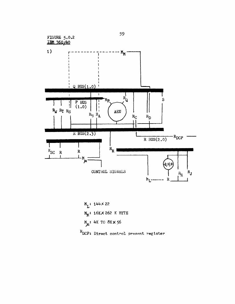
FIGURE 5.0.2
1) - --- -
A DTC 4 I
RSC R R
CONTROL SIGNALS
hL -------
M : 144X 22
16KX 262 K BYTE
1 : 4K TO 8K X 56
RDCP: Direct control present register
RfIR
-MM
R.DCP
2) Field POrt
A
B +
C
D
E
FG
T
M
S
H
R
Q
J
L
N
78
11121314
181920525333
565121
42-2628
3'
29
on
NEXTROMADDRESS
CONSTANT
PART OF NEXT ROM ADDRESS DEPENDSON B ANDID
DETERMINE
E DETERMINE
I WORK WITH
FIELD
NEXT ROM BIT ONE
NEXT ROM BIT ZERO
B
[ CURRENT WORD PARITY|~ALU FUNCTIONS CONTROL
ALU CARRY CONTROL
'ALU OUTPUT CONTROL
(ODD PARITY: THIS WORD
LS ADDRESS CONTROL ( E TO SET ADDRESS, J ANDL TO CONTROL READ AND WRITE)
MM AND MISC CONTROL
Q BUS FROM ALU
R BUS INPUT CONTROL
[R BUS OUTPUT CONTROL
USE WITH R TO SET OR RESET STAT
[EXTENDS FIELDS J AND P
INDICATE SKEW OPTION ON Q BUS INPUT
CT: { 625 n see, 625 n see, 2.5 ja see, 625 n see
I I
L uI jIR- RSERAD- RCON
R tD MBCON
CONTROLSIGNALS
W : -MLI - RCB -MBI -
MLI :ML FOR I/0 CHANNELSft : A DISK UNIT
RSERAD: SERAD REGISTERRIF : INSTRUCTION FETCH
REGISTERRpsy : PSW REGISTERRSDR : 4-vSDR REGISTERMM :8K x 72MB :6K x 72ML 64 x 321B CON: CONSOLE BUFFER
A BINARY OR DECIMAL BYTEADDER AND PACK AND UNPACKLOGIC OPERATOR
FIGURE 50,3IBM 327155
62
BREAK..IN ... BOTH MODE
NEXT ROM BASE ADDRESS
BRANCH CONTROL . BO
A BRANCH - BOTH MO
B BRANCH BOTH MO
Th MODE
PBI
NEXTAADR
NEXTADR B
BRg
ABR
BBR
STAT SETTING-.CPU MODE ONLY
CONTROLS
LEFT ADDER AND MOVER INPUTS.BOTH MODE
RIGHT ADDER AND MOVER INPUTS.BUTH MODE
SPARE BIT
)8 iLOCAL STORE . CPU MODE ONLY
MISCELLANEOUS .CPU MODE ONLY
COUNTERS . CPU MODE ONLY
DE
DE
IOPR
IOSSB
ALU
xU
LSWK
LSRD
IMISC
MISC
IOSS CNT
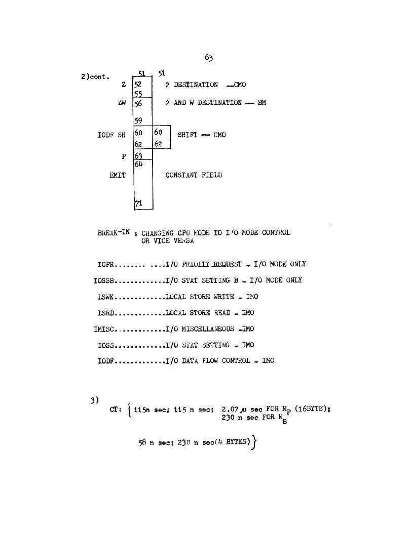
2)cont.z
zw
IODF SH
P
EMIT
BREAK-IN :
2 DESTINATION ....CM
2 AND W DESTINATION - BM
SHIFT - CMO
CONSTANT FIELD
CHANGING CPU MODE TO I/O MODE CONTROLOR VICE VERSA
IOPR ........ .... 1/0 PRIQITY _.REQUEST . I/O MODE ONLY
IOSSB.............I/0 STAT SETTING B . I/O MODE ONLY
LSWK.............LoCAL STORE WRITE . IMO
LSRD..D.........LOCAL STORE READ . IMO
IMISC..........I/O MISCELLANEOUS -IMO
IOSS...........I/0 STAT SETTING . IMO
IODF...........I/O DATA FLOW CONTROL - IMO
))CT: I 115n see; t15 n see; 2.07)u see FOR Mp (16BYTE);
230 n sec FOR MB
58 n sec; 230 n sec(4 BYTES))
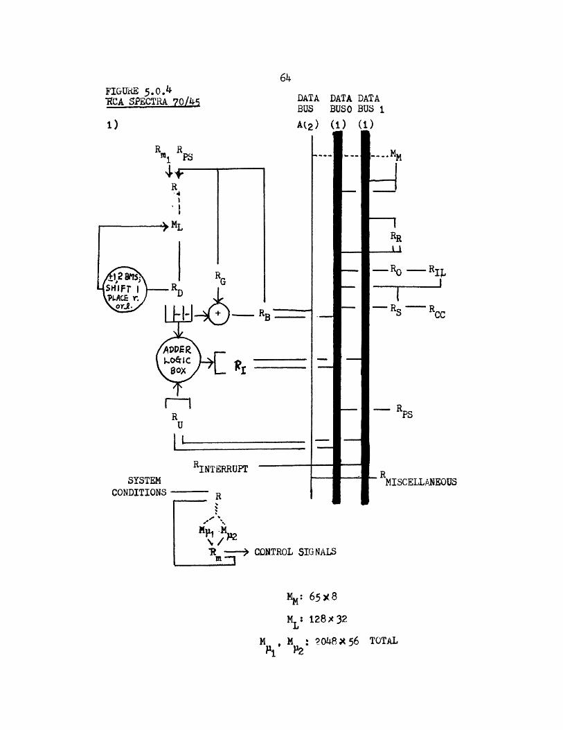
FIGURE 5-0.4XCA SPECTRA 7045 DATA DATA DATA
BUS BUSO BUS 1
AC2) (1- (1)
Rm R
4R
ML
J2 BSSHIFT I RDPLACE r.
* ' ||I
RG
+G
rnl
I'
NTERRUPTSYSTEM
CONDITIONS R
-R --- R
- Rs --- Rcc
-- Rp
RMISCELLANEOUS
CONTROL SIGNALS
MM: 65 X 8
M L: 128) x32
M , M : ?048x56 TOTAL
...- RB . --...
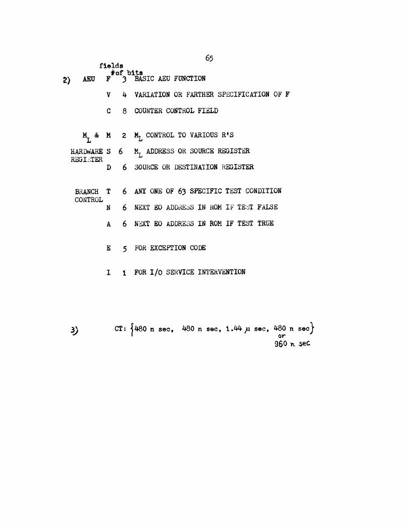
fields#of bits
AEU F 3 BASIC AEU FUNCTION
V 4 VARIATION OR FARTHER SPECIFICATION OF F
C 8 COUNTER CONTROL FIELD
mL &
HARDWAREREGI TER
BRANCH TCONTROL
N
A
E 5
2 ML CONTROL TO VARIOUS R'S
ML ADDRESS OR SOURCE REGISTER
6 SOURCE OR DESTINATION REGISTER
ANY ONE OF 63 SPECIFIC TEST CONDITION
NEXT EO ADDRESS IN ROM IF TEST FALSE
NEXT EO ADDRESS IN ROM IF TEST TRUE
FOR EXCEPTION CODE
I FOR I/O SERVICE INTERVENTION
CT: 480 n see, 480 n see, 1.44 p sec, 480 n sec)or
960 h, seC
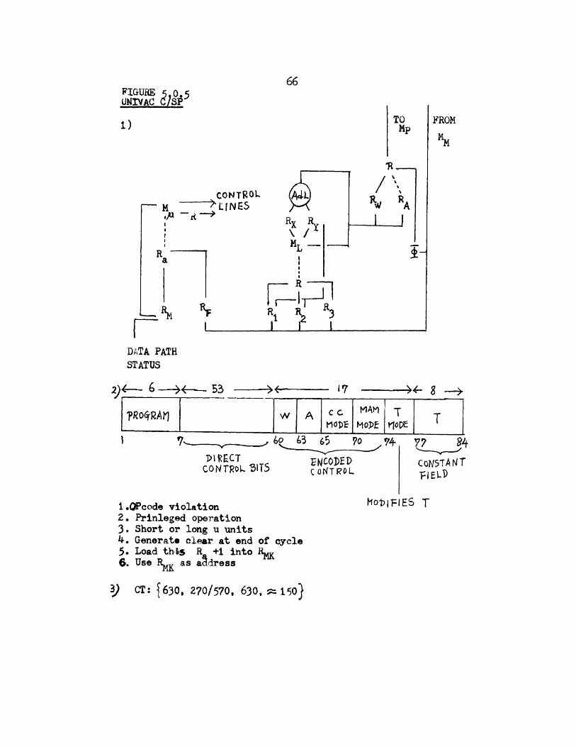
FIGURE 5 A.5UNIVAC C S
TO1) Mp
CONTROL LM L1NES A
RX RY
R ML
F - R
DATA PATHSTATUS
2)4-~ 6 -- +---- 3 ) : 17 )4-;
FROM
?RoqRArJ w A Cc MAM T TMODE MOPE vi0PE7, 6 0 O 74 7
coNTRI C TS ECODED co rANTcON~c<BTS CONTROL pIEO1
I.QPcode violation2. Prinleged operation3. Short or long u units4. Generate clear at end of cycle5. Load thbs R +1 into R'6. Use R as aadress
3) CT: (630, 270/570, 630, = 150)
Hotj-IES T
8 -- )
6. Conclusion
A background in microprogramming has been presented
to introduce a representation scheme and the trade-off
issues. An understanding of a microprocessor is persued
in two aspects: internal and external. First the internal
aspects of a microprocessor are taken up in the three trade
off issues analyzed. The three issues are the ROM word
dimensions, the timing relationships within the micropro-
cessor, and the encoding of ROM bits. Second the external
aspects of a microprocessor are taken up in the represen-
tation scheme, which is consisted of three components:
the structure representation, the transfer constraint,
and the cycle time. The representation scheme attempts
to represent a microprocessor in concise terms for easy
comparison with other microprocessors.
The analysis done in chapter 4 may be reconsidered
now. Many assumptions are idealized to bring out the
prominent deciding factors in the trade-offs. No attempts
have been made to cover all the factors. It can be seen
from the formulation of the trade-off problems that other
factors contributing to the design may be easily incor-
porated. This only lengthens the process of analysis.
As for the representation scheme, it is onlya scheme to
represent the microprocessor. This may serve as an
68
introduction to a more superior scheme.
It is hoped that the analysis of the trade-off issues
may provide concrete guidelines and directions in some
practical design problems in microprogramming. Though
other trade-off issues have not been covered, the ap-
proach presented here may be applied to them as well.
Finally it is hoped that the thesis can stimulate interest
in microprogramming and its related areas.
69
BIBLIOGRAPHY
(1). Mussell, H. A. and Frizzell, C. E. " Stored Program"
IBM - TR - 00.05.015.037, December, 1949.
(2). Wilkes, M.V. "The Best Way to Design an Automatic
Calculating Machine." Report of Manchester University
Computer Inaugural Conference, July, 1951, p16-2 1 .
(3). Wilkes, M.V. "The Growth of Interest in Microprogram-
ming: A Literature Survey." Computing Surveys Vol.1,
No. 3, p139-14 5, Sept., 1969.
(4). Husson, S. S. Microprogramming: Principles and
Practices Prentice-Hall, Inc., Englewood Cliffs,
New Jersey, 1970.
(5). Madnick, S. E. and Toong, H. D. "Design and
Construction of a Pedagogical Microprogrammable
Computer." Third Annual Workshop on Microprogramming,
October 12-13, 1970, Buffalo, New York.
(6). Bell, C. G. and Newell, A. Computer Structures:
Readings and Examples. New York McGraw - Hill, 1971.
(7). Rosin, R. F. "Contemporary Concepts of Microprogram-
ming and Emulation." Computing Survey Vol.1, No.4,
December, 1969.
(8). Hoff, G. " Design of Microprogrammed Control for
General Purpose Processors." IEEE Computer Conference,
September, 1971.
70
(9). Van der Poel, W. L. "Zebra, A Simple Binary Computer."
Information Processing, Proc. Int. Conf. on Informa-
tion Processing, UNESCO, 1959, Butterwirths, London,
p361.
(10).Beckman, F. S., Brooks, F. P., and Lawless, W. J.,
"Developments in the Logical Organization of Computer
Arithmetic and Control Units." Proc. IRE 49 (1961),53.
(11).Dennis, J. B. and Patil, S. S. Computation Structure
Notes for subject 6.232, Department of Electrical
Engineering, M.I.T., Cambridge, Massachusetts, 1971.
(12).Tucker, S. G. "Microprogram Control for System/360."
IBM System Journal, Vol. 6, No. 4, p222 -24 1 , 1967.
(13).Flagg, P., et al. "IBM System/360 Engineering"
Proceeding Fall Joint Computer Conference, 1964.
(14).Redfield, S. R. " A Study in Microprogrammed
Processors: A Medium sized Microprogrammed Processor"
IEEE Transactions on Computers, Vol.c-20, No. 7,
July, 1971.
(15).Beisner, A. M., "Microprogramming Study Report."
Department of Computer Mathematics, Center for
Exploratory studies, IBM - Federal Systems Division
Rockville, Naryland (September 1, 1966)
(16).Rodriguez, J. E., A graph Model for Parallel
Computations, ESL-R-398 MAC-TR-64 September, 1969
M. I. T.
(17).System/370 Model 155 Theory of Operation/Diagram
Manual, IBM Maintenance Library. Form SY 22-6860-0
(18).Wilkes, M. V. "Microprogramming." Proc. Eastern
Joint Comput. Conf., Dec. 1958. Spartan Books,
New York, p.18 .
(19).Kleir, R. L. & Ramamoorthy, C. V. "Optimization
Strategies for Microprograms." IEEE Transactions
on Computers, July, 1972. Volume c-20, Number 7
IEEE Inc. New York.
(20).Tucker, S. G. Emulation of large systems. Comm.
ACM 8, 12 (Dec.1965), p.753-76 1 .
(21).Glantz, H. T. "A note on microprogramming." J.ACM 3,
1(Jan. 1956), p.77-84.
(22).Mercer, R. J. "Micro-Programming." J. ACM 4, 2
(April, 1957), p. 157-171.
(23).Weher, H. "A Microprogrammed implementation of
EULER on IBM System /360 Model 30. Comm. ACM 10,
9 (Sept., 1967), p. 549-558.
Related Documents