© Copyright maxEmbedded 2011 maxEmbedded.wordpress.com 1 Analog to Digital Conversion Most real world data is analog. Whether it be temperature, pressure, voltage, etc, their variation is always analog in nature. For example, the temperature inside a boiler is around 800°C. During its light-up, the temperature never approaches directly to 800°C. If the ambient temperature is 400°C, it will start increasing gradually to 450°C, 500°C and thus reaches 800°C over a period of time. This is an analog data. Now, we must process the data that we have received. But analog signal processing is quite inefficient in terms of accuracy, speed and desired output. Hence, we convert them to digital form using an Analog to Digital Converter (ADC). Signal Acquisition Process In general, the signal (or data) acquisition process has 3 steps. In the Real World, a sensor senses any physical parameter and converts into an equivalent analog electrical signal. For efficient and ease of signal processing, this analog signal is converted into a digital signal using an Analog to Digital Converter (ADC). This digital signal is then fed to the Microcontroller (MCU) and is processed accordingly. Interfacing Sensors In general, sensors provide with analog output, but a MCU is a digital one. Hence we need to use ADC. For simple circuits, comparator op-amps can be used. But even this won’t be required if we use a MCU. We can straightaway use the inbuilt ADC of the MCU. In ATMEGA16/32, PORTA contains the ADC pins. Figure 1: Signal Acquisition Process Figure 2: ADC Pins of ATMEGA16/32

Welcome message from author
This document is posted to help you gain knowledge. Please leave a comment to let me know what you think about it! Share it to your friends and learn new things together.
Transcript
© Copyright maxEmbedded 2011 maxEmbedded.wordpress.com
1
Analog to Digital Conversion
Most real world data is analog. Whether it be temperature, pressure,
voltage, etc, their variation is always analog in nature. For example,
the temperature inside a boiler is around 800°C. During its light-up,
the temperature never approaches directly to 800°C. If the ambient
temperature is 400°C, it will start increasing gradually to 450°C,
500°C and thus reaches 800°C over a period of time. This is an
analog data.
Now, we must process the data that we have
received. But analog signal processing is quite
inefficient in terms of accuracy, speed and
desired output. Hence, we convert them to
digital form using an Analog to Digital
Converter (ADC).
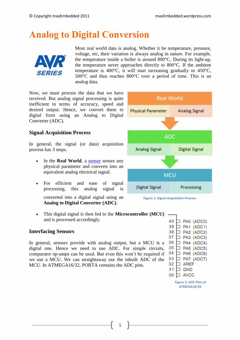
Signal Acquisition Process
In general, the signal (or data) acquisition
process has 3 steps.
In the Real World, a sensor senses any
physical parameter and converts into an
equivalent analog electrical signal.
For efficient and ease of signal
processing, this analog signal is
converted into a digital signal using an
Analog to Digital Converter (ADC).
This digital signal is then fed to the Microcontroller (MCU)
and is processed accordingly.
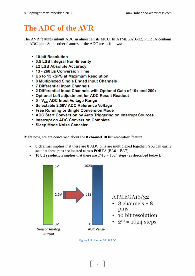
Interfacing Sensors
In general, sensors provide with analog output, but a MCU is a
digital one. Hence we need to use ADC. For simple circuits,
comparator op-amps can be used. But even this won’t be required if
we use a MCU. We can straightaway use the inbuilt ADC of the
MCU. In ATMEGA16/32, PORTA contains the ADC pins.
Figure 1: Signal Acquisition Process
Figure 2: ADC Pins of ATMEGA16/32
© Copyright maxEmbedded 2011 maxEmbedded.wordpress.com
2
The ADC of the AVR
The AVR features inbuilt ADC in almost all its MCU. In ATMEGA16/32, PORTA contains
the ADC pins. Some other features of the ADC are as follows:
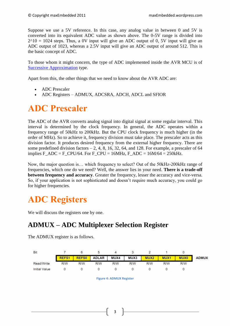
Right now, we are concerned about the 8 channel 10 bit resolution feature.
8 channel implies that there are 8 ADC pins are multiplexed together. You can easily
see that these pins are located across PORTA (PA0…PA7).
10 bit resolution implies that there are 2^10 = 1024 steps (as described below).
Figure 3: 8 channel 10 bit ADC
© Copyright maxEmbedded 2011 maxEmbedded.wordpress.com
3
Suppose we use a 5V reference. In this case, any analog value in between 0 and 5V is
converted into its equivalent ADC value as shown above. The 0-5V range is divided into
2^10 = 1024 steps. Thus, a 0V input will give an ADC output of 0, 5V input will give an
ADC output of 1023, whereas a 2.5V input will give an ADC output of around 512. This is
the basic concept of ADC.
To those whom it might concern, the type of ADC implemented inside the AVR MCU is of
Successive Approximation type.
Apart from this, the other things that we need to know about the AVR ADC are:
ADC Prescaler
ADC Registers – ADMUX, ADCSRA, ADCH, ADCL and SFIOR
ADC Prescaler
The ADC of the AVR converts analog signal into digital signal at some regular interval. This
interval is determined by the clock frequency. In general, the ADC operates within a
frequency range of 50kHz to 200kHz. But the CPU clock frequency is much higher (in the
order of MHz). So to achieve it, frequency division must take place. The prescaler acts as this
division factor. It produces desired frequency from the external higher frequency. There are
some predefined division factors – 2, 4, 8, 16, 32, 64, and 128. For example, a prescaler of 64
implies F_ADC = F_CPU/64. For F_CPU = 16MHz, F_ADC = 16M/64 = 250kHz.
Now, the major question is… which frequency to select? Out of the 50kHz-200kHz range of
frequencies, which one do we need? Well, the answer lies in your need. There is a trade-off
between frequency and accuracy. Greater the frequency, lesser the accuracy and vice-versa.
So, if your application is not sophisticated and doesn’t require much accuracy, you could go
for higher frequencies.
ADC Registers
We will discuss the registers one by one.
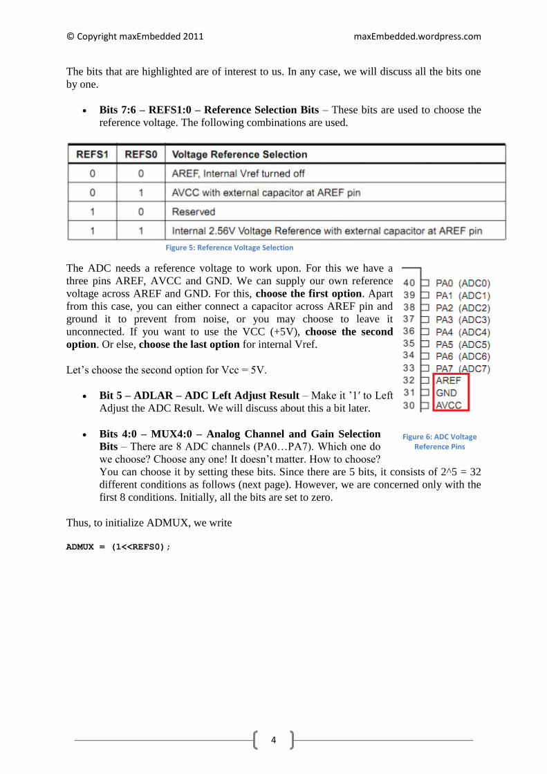
ADMUX – ADC Multiplexer Selection Register
The ADMUX register is as follows.
Figure 4: ADMUX Register
© Copyright maxEmbedded 2011 maxEmbedded.wordpress.com
4
The bits that are highlighted are of interest to us. In any case, we will discuss all the bits one
by one.
Bits 7:6 – REFS1:0 – Reference Selection Bits – These bits are used to choose the
reference voltage. The following combinations are used.
Figure 5: Reference Voltage Selection
The ADC needs a reference voltage to work upon. For this we have a
three pins AREF, AVCC and GND. We can supply our own reference
voltage across AREF and GND. For this, choose the first option. Apart
from this case, you can either connect a capacitor across AREF pin and
ground it to prevent from noise, or you may choose to leave it
unconnected. If you want to use the VCC (+5V), choose the second
option. Or else, choose the last option for internal Vref.
Let’s choose the second option for Vcc = 5V.
Bit 5 – ADLAR – ADC Left Adjust Result – Make it ’1′ to Left
Adjust the ADC Result. We will discuss about this a bit later.
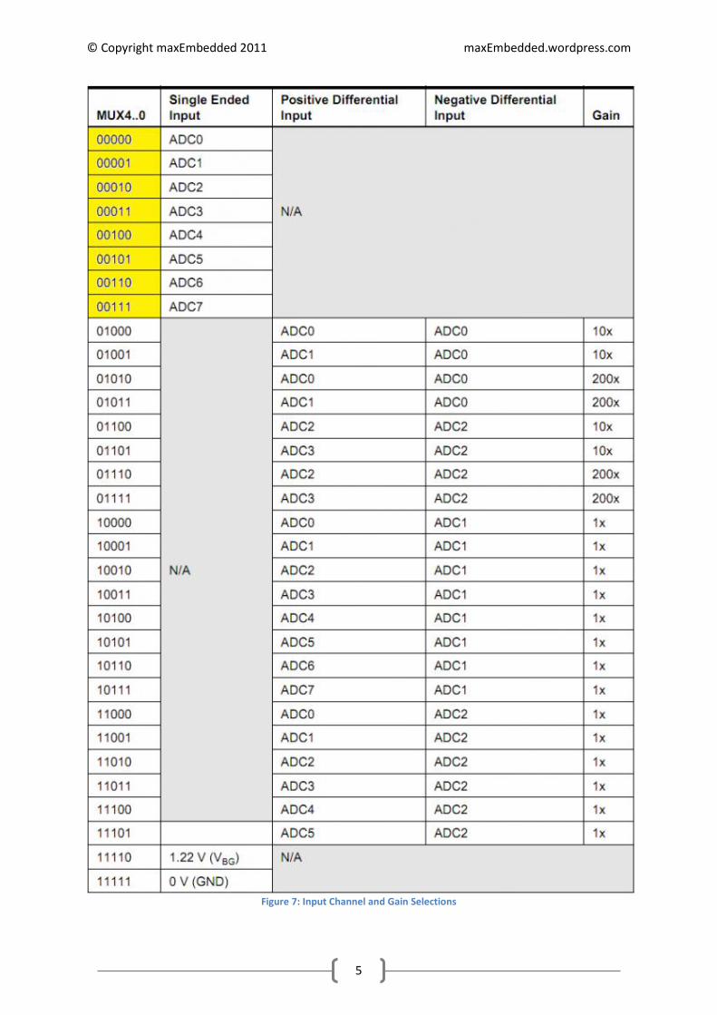
Bits 4:0 – MUX4:0 – Analog Channel and Gain Selection
Bits – There are 8 ADC channels (PA0…PA7). Which one do
we choose? Choose any one! It doesn’t matter. How to choose?
You can choose it by setting these bits. Since there are 5 bits, it consists of 2^5 = 32
different conditions as follows (next page). However, we are concerned only with the
first 8 conditions. Initially, all the bits are set to zero.
Thus, to initialize ADMUX, we write
ADMUX = (1<<REFS0);
Figure 6: ADC Voltage Reference Pins
© Copyright maxEmbedded 2011 maxEmbedded.wordpress.com
5
Figure 7: Input Channel and Gain Selections
© Copyright maxEmbedded 2011 maxEmbedded.wordpress.com
6
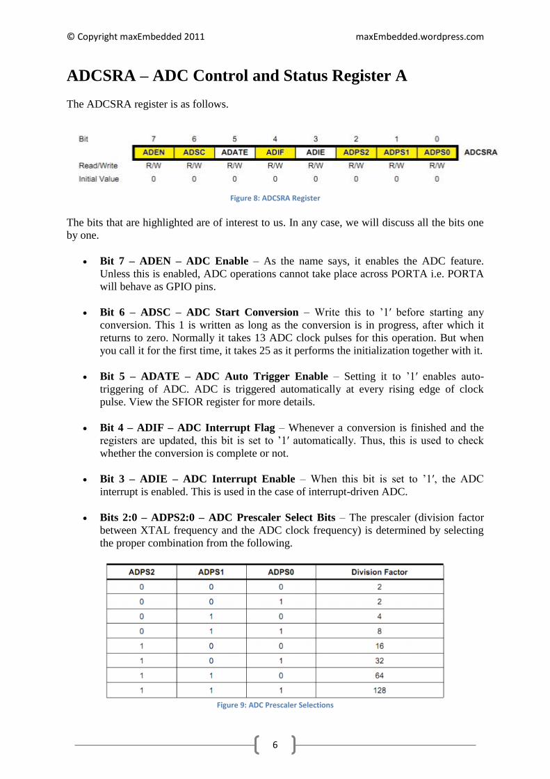
ADCSRA – ADC Control and Status Register A
The ADCSRA register is as follows.
Figure 8: ADCSRA Register
The bits that are highlighted are of interest to us. In any case, we will discuss all the bits one
by one.
Bit 7 – ADEN – ADC Enable – As the name says, it enables the ADC feature.
Unless this is enabled, ADC operations cannot take place across PORTA i.e. PORTA
will behave as GPIO pins.
Bit 6 – ADSC – ADC Start Conversion – Write this to ’1′ before starting any
conversion. This 1 is written as long as the conversion is in progress, after which it
returns to zero. Normally it takes 13 ADC clock pulses for this operation. But when
you call it for the first time, it takes 25 as it performs the initialization together with it.
Bit 5 – ADATE – ADC Auto Trigger Enable – Setting it to ’1′ enables auto-
triggering of ADC. ADC is triggered automatically at every rising edge of clock
pulse. View the SFIOR register for more details.
Bit 4 – ADIF – ADC Interrupt Flag – Whenever a conversion is finished and the
registers are updated, this bit is set to ’1′ automatically. Thus, this is used to check
whether the conversion is complete or not.
Bit 3 – ADIE – ADC Interrupt Enable – When this bit is set to ’1′, the ADC
interrupt is enabled. This is used in the case of interrupt-driven ADC.
Bits 2:0 – ADPS2:0 – ADC Prescaler Select Bits – The prescaler (division factor
between XTAL frequency and the ADC clock frequency) is determined by selecting
the proper combination from the following.
Figure 9: ADC Prescaler Selections
© Copyright maxEmbedded 2011 maxEmbedded.wordpress.com
7
Assuming XTAL frequency of 16MHz and the frequency range of 50kHz-200kHz, we
choose a prescaler of 128.
Thus, F_ADC = 16M/128 = 125kHz.
Thus, we initialize ADCSRA as follows.
ADCSRA = (1<<ADEN)|(1<<ADPS2)|(1<<ADPS1)|(1<<ADPS0); // prescaler = 128
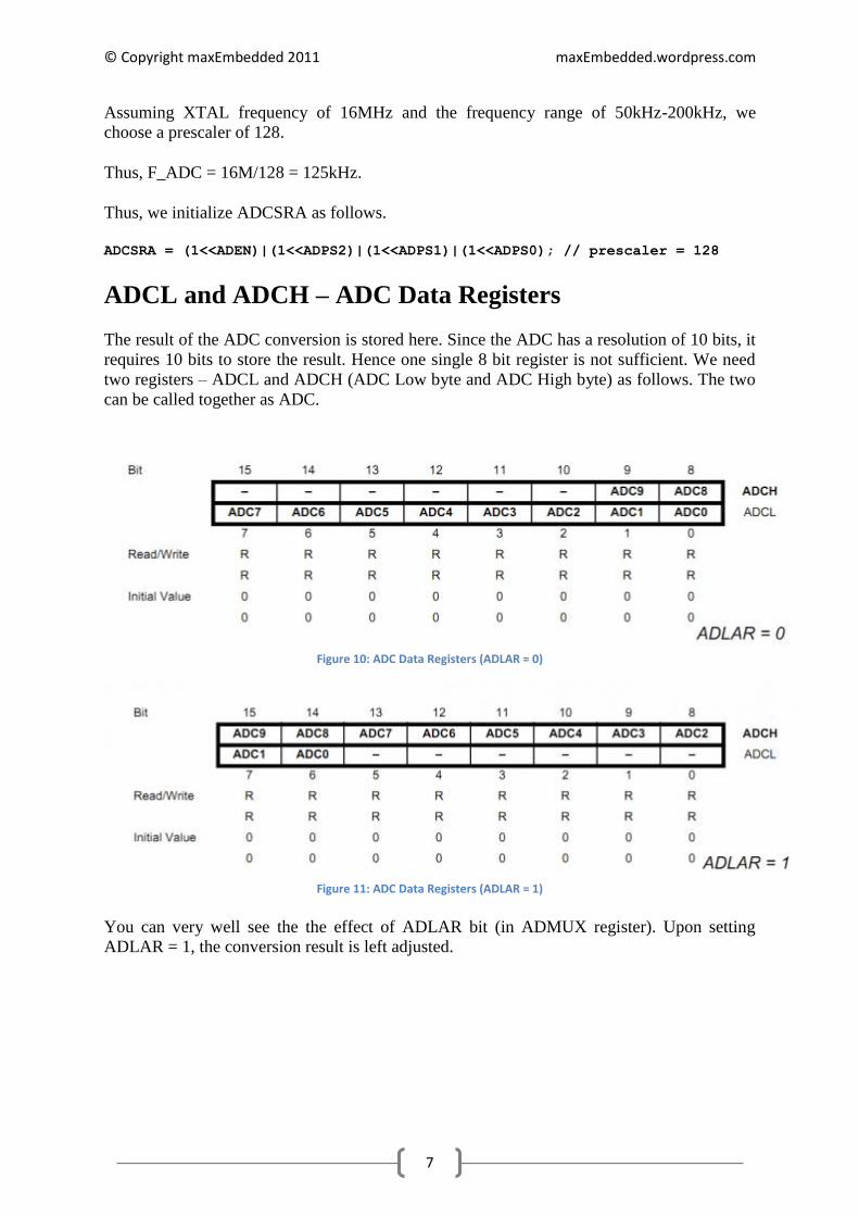
ADCL and ADCH – ADC Data Registers
The result of the ADC conversion is stored here. Since the ADC has a resolution of 10 bits, it
requires 10 bits to store the result. Hence one single 8 bit register is not sufficient. We need
two registers – ADCL and ADCH (ADC Low byte and ADC High byte) as follows. The two
can be called together as ADC.
Figure 10: ADC Data Registers (ADLAR = 0)
Figure 11: ADC Data Registers (ADLAR = 1)
You can very well see the the effect of ADLAR bit (in ADMUX register). Upon setting
ADLAR = 1, the conversion result is left adjusted.
© Copyright maxEmbedded 2011 maxEmbedded.wordpress.com
8
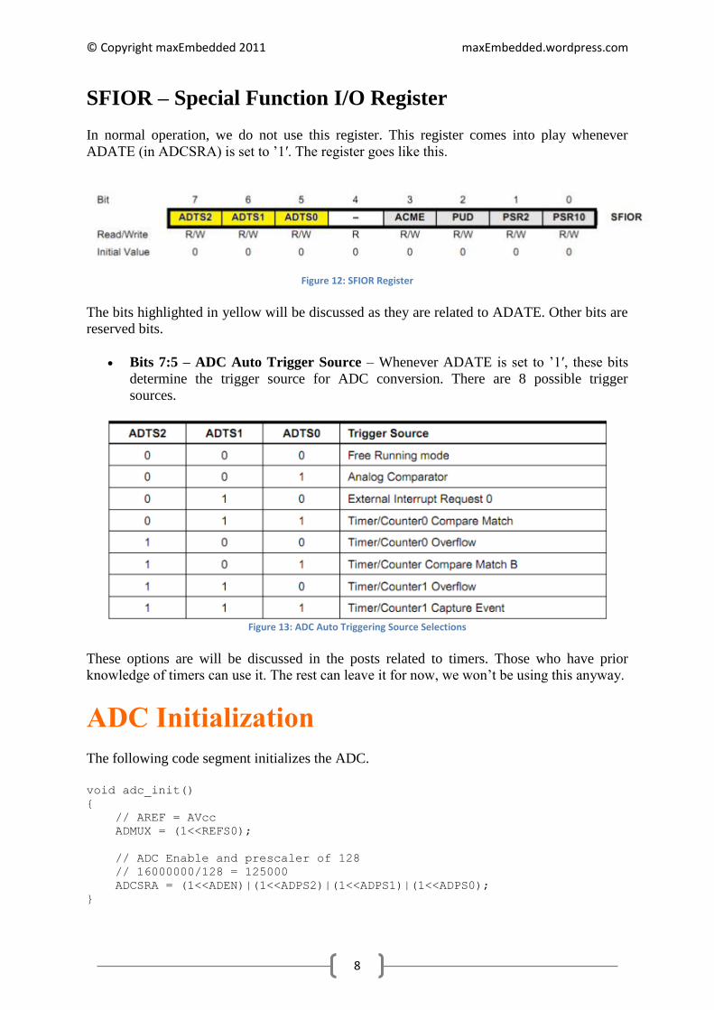
SFIOR – Special Function I/O Register
In normal operation, we do not use this register. This register comes into play whenever
ADATE (in ADCSRA) is set to ’1′. The register goes like this.
Figure 12: SFIOR Register
The bits highlighted in yellow will be discussed as they are related to ADATE. Other bits are
reserved bits.
Bits 7:5 – ADC Auto Trigger Source – Whenever ADATE is set to ’1′, these bits
determine the trigger source for ADC conversion. There are 8 possible trigger
sources.
Figure 13: ADC Auto Triggering Source Selections
These options are will be discussed in the posts related to timers. Those who have prior
knowledge of timers can use it. The rest can leave it for now, we won’t be using this anyway.
ADC Initialization
The following code segment initializes the ADC.
void adc_init()
{
// AREF = AVcc
ADMUX = (1<<REFS0);
// ADC Enable and prescaler of 128
// 16000000/128 = 125000
ADCSRA = (1<<ADEN)|(1<<ADPS2)|(1<<ADPS1)|(1<<ADPS0);
}
© Copyright maxEmbedded 2011 maxEmbedded.wordpress.com
9
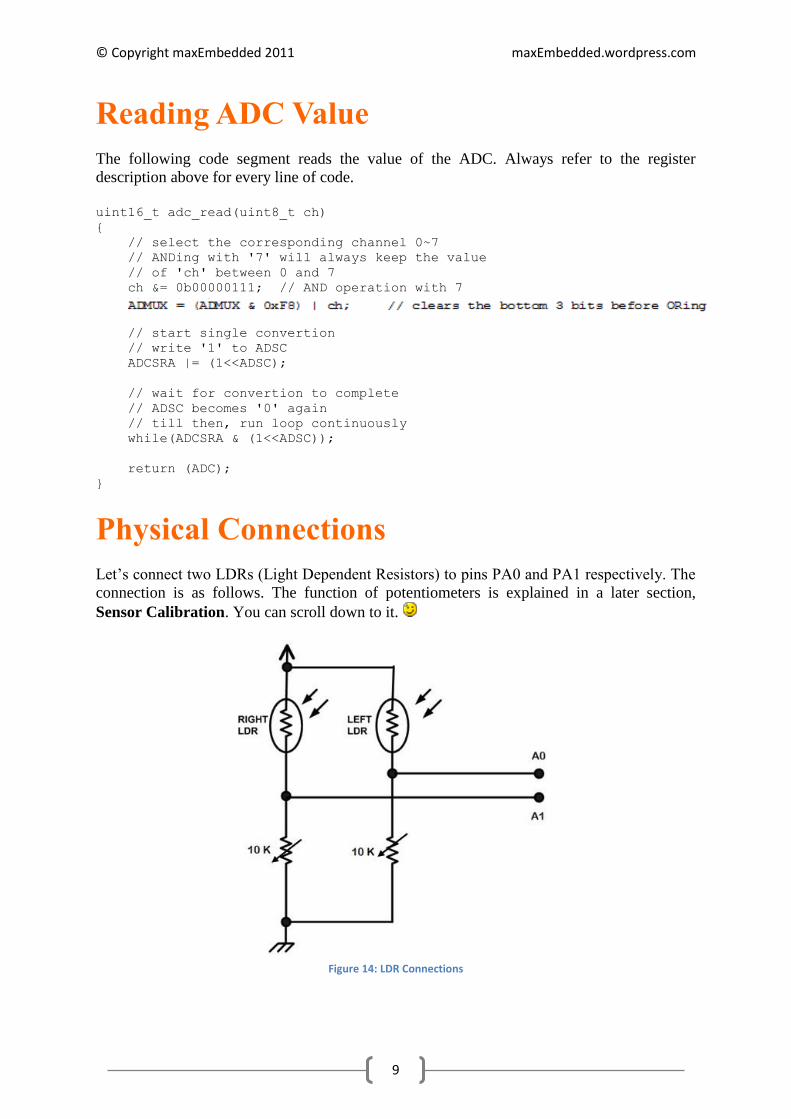
Reading ADC Value
The following code segment reads the value of the ADC. Always refer to the register
description above for every line of code.
uint16_t adc_read(uint8_t ch)
{
// select the corresponding channel 0~7
// ANDing with '7' will always keep the value
// of 'ch' between 0 and 7
ch &= 0b00000111; // AND operation with 7
ADMUX |= ch;
// start single convertion
// write '1' to ADSC
ADCSRA |= (1<<ADSC);
// wait for convertion to complete
// ADSC becomes '0' again
// till then, run loop continuously
while(ADCSRA & (1<<ADSC));
return (ADC);
}
Physical Connections
Let’s connect two LDRs (Light Dependent Resistors) to pins PA0 and PA1 respectively. The
connection is as follows. The function of potentiometers is explained in a later section,
Sensor Calibration. You can scroll down to it.
Figure 14: LDR Connections
© Copyright maxEmbedded 2011 maxEmbedded.wordpress.com
10
Now suppose we want to display the corresponding ADC values in an LCD. So, we also need
to connect an LCD to our MCU. Read this post to know about LCD interfacing.
Since it is an LDR, it senses the intensity of light and accordingly change its resistance. The
resistance decreases exponentially as the light intensity increases. Suppose we also want to
light up an LED whenever the light level decreases. So, we can connect the LED to any one
of the GPIO pins, say PC0.
Note that since the ADC returns values in between 0 and 1023, for dark conditions, the value
should be low (below 100 or 150) whereas for bright conditions, the value should be quite
high (above 900).
Now let’s write the complete code.
Example Code
To learn about LCD interfacing, view this post. You can type, compile and build it in AVR
Studio 5. View this page to know how. To know about the I/O port operations in AVR, view
this page.
#include <avr/io.h>
#include <util/delay.h>
#include "lcd.h"
#define LTHRES 500
#define RTHRES 500
// initialize adc
void adc_init()
{
// AREF = AVcc
ADMUX = (1<<REFS0);
// ADC Enable and prescaler of 128
// 16000000/128 = 125000
ADCSRA = (1<<ADEN)|(1<<ADPS2)|(1<<ADPS1)|(1<<ADPS0);
}
// read adc value
uint16_t adc_read(uint8_t ch)
{
// select the corresponding channel 0~7
// ANDing with '7' will always keep the value
// of 'ch' between 0 and 7
ch &= 0b00000111; // AND operation with 7
ADMUX |= ch;
// start single conversion
// write '1' to ADSC
ADCSRA |= (1<<ADSC);
// wait for conversion to complete
// ADSC becomes '0' again
// till then, run loop continuously
© Copyright maxEmbedded 2011 maxEmbedded.wordpress.com
11
while(ADCSRA & (1<<ADSC));
return (ADC);
}
int main()
{
uint16_t adc_result0, adc_result1;
char int_buffer[10];
DDRC = 0x01; // to connect led to PC0
// initialize adc and lcd
adc_init();
lcd_init(LCD_DISP_ON_CURSOR);
// display the labels on LCD
lcd_puts("left ADC = ");
lcd_gotoxy(0,1);
lcd_puts("right ADC = ");
_delay_ms(50);
while(1)
{
adc_result0 = adc_read(0); // read adc value at PA0
adc_result1 = adc_read(1); // read adc value at PA1
// condition for led to glow
if (adc_result0 < LTHRES && adc_result1 < RTHRES)
PORTC = 0x01;
else
PORTC = 0x00;
// now display on lcd
itoa(adc_result0, int_buffer, 10);
lcd_gotoxy(12,0);
lcd_puts(int_buffer);
itoa(adc_result0, int_buffer, 10);
lcd_gotoxy(12,1);
lcd_puts(int_buffer);
_delay_ms(50);
}
}
Sensor Calibration
Calibration means linking your real world data with the virtual data. In the problem statement
given earlier, I have mentioned that the LED should glow if the light intensity reduces. But
when should it start to glow? The MCU/code doesn’t know by itself. You get the readings
from the sensor continuously in between 0 and 1023. So, the question is how do we know that
below ‘such and such’ level the LED should glow?
This is achieved by calibration. You need to physically set this value. What you do is that you
run the sensor for all the lighting conditions. You have the ADC values for all these levels.
Now, you need to physically see and check the conditions yourself and then apply a
© Copyright maxEmbedded 2011 maxEmbedded.wordpress.com
12
threshold. Below this threshold, the light intensity goes sufficiently down enough for the
LED to glow.
The potentiometer connected in the circuit is also for the same reason. Now, by the basic
knowledge of electronics, you could easily say that upon changing the pot value the ADC
value changes. Thus, for various reasons (like poor lighting conditions, you are unable to
distinguish between bright and dark conditions, etc), you can vary the pot to get desired
results.
This is why I have given the two thresholds (RTHRES anf LTHRES) in the beginning of the
code.
So, this is all with the ADC. I hope you enjoyed reading this. Please post the comments for
any kind of suggestion, doubt, clarification, etc in the homepage or you can also email me.
Other Links
1. LCD Interfacing
http://maxembedded.wordpress.com/2011/06/16/lcd-interfacing-with-avr/
2. Sensor Fundamentals
http://maxembedded.wordpress.com/2011/06/18/sensor-fundamentals/
3. Using AVR Studio 5
http://maxembedded.wordpress.com/2011/06/12/using-avr-studio-5/
4. I/O Port Operations in AVR
http://maxembedded.wordpress.com/2011/06/10/port-operations-in-avr/
5. maxEmbedded Homepage
http://maxembedded.wordpress.com/
6. The ADC of the AVR (This article)
http://maxembedded.wordpress.com/2011/06/20/the-adc-of-the-avr/
Written By
Mayank Prasad
maxEmbedded.wordpress.com
Related Documents