Permission is hereby granted to the University of Alberta Libraries to reproduce single copies of this thesis and to lend or sell such copies for private, scholarly or scientific research purposes only. Where the thesis is converted to, or otherwise made available in digital form, the University of Alberta will advise potential users of the thesis of these terms. The author reserves all other publication and other rights in association with the copyright in the thesis and, except as herein before provided, neither the thesis nor any substantial portion thereof may be printed or otherwise reproduced in any material form whatsoever without the author's prior written permission. University of Alberta Materials Characterization and Growth Mechanisms of ZnO, ZrO 2 , and HfO 2 Deposited by Atomic Layer Deposition by Amir Afshar A thesis submitted to the Faculty of Graduate Studies and Research in partial fulfillment of the requirements for the degree of Doctor of Philosophy in Materials Engineering Department of Chemical and Materials Engineering © Amir Afshar Spring 2014 Edmonton, Alberta

Welcome message from author
This document is posted to help you gain knowledge. Please leave a comment to let me know what you think about it! Share it to your friends and learn new things together.
Transcript
Permission is hereby granted to the University of Alberta Libraries to reproduce single copies of this
thesis and to lend or sell such copies for private, scholarly or scientific research purposes only. Where
the thesis is converted to, or otherwise made available in digital form, the University of Alberta
will advise potential users of the thesis of these terms.
The author reserves all other publication and other rights in association with the copyright in the thesis
and, except as herein before provided, neither the thesis nor any substantial portion thereof may be printed
or otherwise reproduced in any material form whatsoever without the author's prior written permission.
University of Alberta
Materials Characterization and Growth Mechanisms of ZnO, ZrO2, and HfO2 Deposited by
Atomic Layer Deposition
by
Amir Afshar
A thesis submitted to the Faculty of Graduate Studies and Research
in partial fulfillment of the requirements for the degree of
Doctor of Philosophy
in
Materials Engineering
Department of Chemical and Materials Engineering
© Amir Afshar
Spring 2014
Edmonton, Alberta

To my wonderful wife, Arezou, who has always been there inspiring me to do
better.
And to my parents, Mahrokh and Esmaeil, and to my sisters, Azin and Ada.
Abstract
Gallium Nitride (GaN) is recognized as one of the best candidates for high-
power high-frequency metal-oxide-semiconductor field-effect-transistors
(MOSFETs). The critical component to enable this technology is the development
of a robust oxide with low density of defects and preferential mobility properties
that can produce an enhancement mode transistor rather than a depletion mode
transistor. Zirconium oxide (ZrO2) and hafnium oxide (HfO2) are considered as
two promising oxides for the gate oxide of the GaN MOSFETs. On the other hand,
zinc oxide (ZnO) is an alternative wide bandgap semiconductor for GaN. ZnO has
some advantages over GaN in optoelectronics due to its large exciton binding
energy (~60 meV), and is widely used as the active channel in thin film transistors
(TFTs). To control the electrical properties of the deposited thin films, a
fundamental understanding of the nucleation and growth mechanisms is essential.
In this dissertation, the material characterization and growth mechanisms of
atomic layer deposition (ALD) of the three important oxides in semiconductor
industry, ZnO, ZrO2, and HfO2, were investigated. The oxides were deposited
using thermal and plasma-enhanced ALD on Si(100) substrate at various
deposition temperatures. Different analytical techniques, including spectroscopic
ellipsometry (SE), X-ray photoelectron spectroscopy (XPS), X-ray diffraction
(XRD), atomic force microscopy (AFM), and transmission electron microscopy
(TEM) were utilized to analyze the optical, chemical, and morphological
characteristics of the oxide thin films. Based on the results, nucleation and growth
mechanisms were proposed for thermal and plasma enhanced ALD of ZnO, ZrO2,
and HfO2. The role of ALD parameters, as well as –OH reaction sites on the
nucleation and growth mechanisms were described. Atomistic growth
mechanisms of thermal ALD ZnO, ZrO2, and HfO2 were studied using a density
functional theory (DFT) approach. The important role of formation of
intermediate structures between surface reaction sites and the precursor molecules
were emphasized. The results were found to be consistent with the variation of
growth rate of the ALD oxides with the deposition temperature. Finally, it was
found that PEALD ZrO2 offered the best properties for the gate oxide of the GaN
MOSFETs with the lowest value of density of interface traps.
Acknowledgments
This thesis would never come to existence without support and assistance from
many individuals. I would like to gratefully thank my supervisor Dr. Ken Cadien
for his support, enthusiastic guidance, inspiration, and patience throughout my
PhD program. I would also like to thank Dr. Douglas Barlage for his advice, and
encouragements along my study. I am also grateful to the examining committee
members, Dr. John Nychka, Dr. Vinay Prasad, and Dr. David Emslie for their
insightful comments on my thesis.
Much of the work I did was the results of collaborations with my fellow
colleagues. I would like to especially thank Dr. Ali Foroughi, Triratna Muneshwar,
Kyle Bothe, Peter von Hauff, Alex Ma, Gem Shoute, Mei Shen, Dr. Manisha
Gupta, Mourad Benlarmi, Alireza Kohan Dehghan, and Dr. Farshid Vejahati, for
many insightful debates and ideas.
I am grateful to Dr. Bruce Rayner, Noel O'Toole, and Don Fillipelli from Kurt
J. Lesker for their time on training me on the atomic layer deposition system and
also helping me in troubleshooting the system.
I would like to thank the faculty and staff of the Department of Chemical and
Materials Engineering, especially Lily Laser, Mia Law, Marion Pritchard, and
Kevin Heidebrecht for all the provided fundamental administrative and technical
assistance to me.
I would like to thank my beloved wife, Arezou Elliyoon, for her patience,
support, and encouragements throughout my PhD studies and also helping me

with drawing the schematic figures in this thesis. Lastly, I would like to thank my
parents and my sisters for their constant support throughout the course of my
studies.
Table of Contents
1. Introduction ........................................................................................................ 1
1.1 Background ............................................................................................... 1
1.2 Literature Review ..................................................................................... 2
1.2.1 Zinc Oxide (ZnO) ......................................................................... 2
1.2.2 Gallium Nitride (GaN) ................................................................. 2
1.2.3 GaN-Based Transistors ................................................................ 4
1.2.4 MOSFET Operation and Interface Oxides ................................... 6
1.2.5 Gate Oxide Materials for GaN MOSFETs ................................... 7
1.2.6 Heterojunction Band Alignment .................................................. 9
1.2.7 Previous Studies on Dielectric Materials for GaN MOSFETs .. 10
1.2.8 Atomic Layer Deposition (ALD) of Oxides .............................. 15
1.3 Objectives of This Work......................................................................... 18
1.4 Outline of Thesis .................................................................................... 19
2. Theoretical Background of Quantum Chemistry Calculations ................... 20
2.1 Schrödinger Equation for a Many-Body System .................................... 20
2.2 Born-Oppenheimer Approximation and Variational Theorem .............. 22
2.3 Basis Functions ....................................................................................... 23
2.4 Molecular Orbital Methods – Hartree-Fock ........................................... 25
2.5 Density Functional Theory ..................................................................... 27
2.6 Geometry Optimization and Frequency Calculations ............................ 29
2.7 Computational Chemistry Approach to Atomic Layer Deposition ........ 30
2.8 Computational Method in This Thesis ................................................... 31
3. Experimental Procedures ................................................................................ 32
3.1 ALD Reactor .......................................................................................... 32
3.2 Sample Preparation ................................................................................. 35
3.3 In-Situ Spectroscopic Ellipsometry ........................................................ 36
3.4 Atomic Force Microscopy (AFM) .......................................................... 38
3.5 X-Ray Photoelectron (XPS) Analyses .................................................... 40
3.6 X-Ray Diffraction (XRD) Analyses ....................................................... 41
4. Atomic Layer Deposition of Zinc Oxide ........................................................ 43
4.1 Introduction ............................................................................................ 43
4.2 Experimental Procedure and Theoretical Model .................................... 45
4.3 Results and Discussion ........................................................................... 46
4.3.1 Optical Constants ....................................................................... 46
4.3.2 Saturation curves and GPC ........................................................ 50
4.3.3 Chemical Composition ............................................................... 52
4.3.4 Roughness .................................................................................. 56
4.3.5 Crystallinity ................................................................................ 59
4.3.6 Electrical Resistivity .................................................................. 62
4.4 Growth Mechanism of TALD ZnO: DFT Approach.............................. 64
4.5 Conclusions ............................................................................................ 76
5. Atomic Layer Deposition of Zirconium Oxide .............................................. 77
5.1 Introduction ............................................................................................ 77
5.2 Experimental Procedure ......................................................................... 78
5.3 Results .................................................................................................... 79
5.3.1 Optical Constants ....................................................................... 79
5.3.2 Growth Rate and Saturation Curves ........................................... 81
5.3.3 Chemical Composition ............................................................... 83
5.3.4 Roughness .................................................................................. 86
5.3.5 Crystallinity ................................................................................ 88
5.4 Characterization of Cr/ZrO2/GaN MOS ................................................. 90
5.5 Growth Mechanism of TALD ZrO2: DFT Approach ............................. 92
5.6 Conclusions .......................................................................................... 103
6. Atomic Layer Deposition of Hafnium Oxide ............................................... 105
6.1 Introduction .......................................................................................... 105
6.2 Experimental Procedure and Computational Calculations ................... 107
6.3 Results .................................................................................................. 107
6.3.1 Optical Constants ..................................................................... 107
6.3.2 Growth Per Cycle (GPC) ......................................................... 110
6.3.3 Chemical Composition ............................................................. 111
6.3.4 Roughness and Crystallinity .................................................... 115
6.4 Characterization of Cr/HfO2/GaN MOS .............................................. 117
6.5 Growth Mechanism of TALD HfO2: DFT Approach .......................... 118
6.6 Conclusions .......................................................................................... 128
7. Conclusions and Future Work ...................................................................... 130
7.1 Summary of Contributions to Knowledge ............................................ 133
7.2 Future Work .......................................................................................... 134
Bibliography ....................................................................................................... 136
List of Tables
Table 1.1 Some GaN characteristics ....................................................................... 4
Table 1.2 FOM for various semiconductors normalized with respect Si ............... 5
Table 1.3 Calculated band offsets of dielectrics on GaN (eV) ............................ 10
Table 1.4 A summary of some of the properties of dielectric materials used as the
gate oxide of the GaN MOSFETs ......................................................... 15
Table 3.1 Flow rates of ALD line for deposition of the ALD oxides (sccm) ....... 34
Table 3.2 Calibration table for the setpoint of the substrate temperature ............. 36
Table 3.3 The temperature of the various parts of the ALD system during the
deposition .............................................................................................................. 36
Table 4.1 Optical bandgap of ALD ZnO at various deposition temperatures ...... 48
Table 4.2 Chemical compositions of ZnO films (at.%) deposited at various
temperatures using thermal and plasma-enhanced ALD ....................... 55
Table 4.3 RMS Roughness parameters of the TALD and PEALD ZnO deposited
at various temperatures .......................................................................... 56
Table 4.4 Average grain size of ALD ZnO films (nm) ......................................... 58
Table 4.5 Variation of GPC with the substrate temperature for the ALD
of ZnO ................................................................................................... 64
Table 4.6 Effect of cluster size on the half-reactions energies and the geometry of
structures 6 and 11 ................................................................................. 73
Table 5.1 Chemical composition of zirconium oxide samples deposited by TALD
and PEALD at various temperatures ..................................................... 86
Table 5.2 RMS Roughness of the TALD and PEALD ZrO2 deposited at various
temperatures (nm) .................................................................................. 86
Table 6.1 Chemical compositions of hafnium oxide samples deposited by TALD
and PEALD at various temperatures ................................................... 114
Table 6.2 RMS Roughness of the TALD and PEALD HfO2 deposited at various
temperatures (nm) ................................................................................ 115
List of Figures
Figure 1.1 Schematic diagrams of wurtzite (a) and zincblende (b) crystal
structures... ............................................................................................ 4
Figure 1.2 Schematic view of an n-channel MOSFET. .......................................... 6
Figure 1.3 Possible band alignments of two semiconductors in contact: (a) type I,
(b) type II, staggered, and (c) type III, broken gap alignments. .......... 10
Figure 1.4 Schematic representation of an ALD cycle. ........................................ 16
Figure 1.5 Schematic of ALD window and possible behavior of ALD growth. .. 17
Figure 2.1 A system of two nuclei and two electrons. α and β are nuclei and i and
j represent the electrons in the system................................................. 22
Figure 3.1 Views of (a) the ALD-150LX system and (b) the inside of the ALD
cabinet. 1:Load-lock; 2: ALD cabinet; 3: ALD chamber; 4: Plasma
Source; 5: Ampoule heater box; 6: Water ampoule. ........................... 33
Figure 3.2 Schematic view of the ALD system. ................................................... 33
Figure 3.3 A Schematic view of SE. ..................................................................... 37
Figure 3.4 A Schematic view of the SE mounted on the ALD chamber. The
plasma source on top of the chamber was not shown in this figure. ... 37
Figure 4.1 Refractive index (a,b) and extinction coefficient (c,d) of TALD (a,c)
and PEALD (b,d) ZnO at the deposition temperature. For more clarity
the refractive index and extinction coefficient of the samples
deposited at 200 °C are shown in (e, f). .............................................. 47
Figure 4.2 Illustration of the procedure of finding the optical bandgap of PEALD
ZnO at 100 °C. .................................................................................... 48
Figure 4.3 Effect of temperature on the optical bandgap of TALD ZnO deposited
at 200 °C. ............................................................................................. 49
Figure 4.4 Variation of GPC vs. DEZ (a), H2O (b), and oxygen plasma (c)
exposure times for ALD of ZnO at 100 °C. ........................................ 51
Figure 4.5 Variation of GPC with deposition temperature for TALD and PEALD
of ZnO. ................................................................................................ 52
Figure 4.6 High Resolution XPS graphs of Zn2p (a), O1s (b), and C1s (c), for
ALD ZnO with different deposition conditions. ................................. 54
Figure 4.7 Average RMS roughness of the ALD ZnO thin films vs. the deposition
temperature. ......................................................................................... 56
Figure 4.8 AFM surface plots of the ALD ZnO deposited at different
temperatures using thermal and plasma-enhanced approaches. .......... 58
Figure 4.9 Average grain size of ALD ZnO films vs. the deposition temperature.59
Figure 4.10 XRD profiles of the TALD and PEALD ZnO samples deposited at
various temperatures. ........................................................................ 60
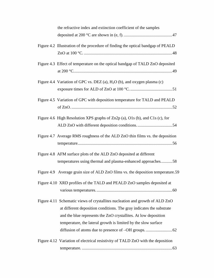
Figure 4.11 Schematic views of crystallites nucleation and growth of ALD ZnO
at different deposition conditions. The gray indicates the substrate
and the blue represents the ZnO crystallites. At low deposition
temperature, the lateral growth is limited by the slow surface
diffusion of atoms due to presence of –OH groups. ......................... 62
Figure 4.12 Variation of electrical resistivity of TALD ZnO with the deposition
temperature. ...................................................................................... 63
Figure 4.13 Reaction pathway of DEZ half-reaction. The white spheres represent
H, red: O, black: C, and blue: Zn atoms. The bond lengths and
angles are reported in Å and degrees. ............................................... 66
Figure 4.14 Potential energy surface for the DEZ half-reaction. The calculations
were carried out at the B3LYP/6-311G(d) level. The enthalpy values
are reported at 0 K. For clarity, the ZnO structure in the reactions is
shown with a smaller cluster. ............................................................ 67
Figure 4.15 Reaction pathway of H2O half-reaction. The white spheres represent
H, red: O, black: C, and blue: Zn atoms. The bond lengths and
angles are reported in Å and degrees. ............................................... 69
Figure 4.16 PES of H2O half-reaction. All the calculations were carried out at the
B3LYP/6-311G(d) level. The enthalpy values are reported at 0 K. 70
Figure 4.17 PES of H2O half-reaction and the structure of AS-8, calculated at the
B3LYP/6-31G(d) level. The enthalpy values are reported at zero
Kelvin. .............................................................................................. 70
Figure 4.18 The structure of the ZnO cluster models, which were used to study
the effect of near neighbor atoms on the ZnO ALD half-reactions. . 72
Figure 4.19 Temperature-dependent variation of GPC, and Gibbs free energies of
adsorption of DEZ and H2O during ALD of ZnO. The rate of
variation of GPC with temperature changes approximately at the
same temperature that the Gibbs free energies of adsorption of
precursors become positive. .............................................................. 75
Figure 5.1 Refractive index (a,b) and extinction coefficient (c,d) of TALD (a,c)
and PEALD (b,d) ZrO2 vs. the incident photon energy and ALD
temperatures. For more clarity the refractive index and extinction
coefficient of the samples deposited at 200 °C are shown in (e, f). .... 80
Figure 5.2 Saturation curves for the TDMAZr (a), H2O (b), and (c) O2-Plasma at
200 °C. ................................................................................................ 82
Figure 5.3 GPC of ALD ZrO2 with deposition temperature for both thermal and
plasma-enhanced processes. ................................................................ 83
Figure 5.4 High Resolution XPS graphs of Zr3d (a), O1s (b), and C1s (c) for
ALD ZrO2 at different deposition conditions...................................... 84
Figure 5.5 AFM surface plots of the ALD ZrO2 deposited at different
temperatures using thermal and plasma-enhanced approaches. .......... 87
Figure 5.6 XRD profiles of the ALD ZrO2 samples deposited by thermal and
plasma-enhanced ALD processes at different deposition temperatures.89
Figure 5.7 A schematic model for crystallites nucleation and growth in ZrO2 and
HfO2 thin films fabricated by ALD. The grey, orange, and black areas
show the substrate, amorphous phase, and crystalline phase of the
ALD oxides. ........................................................................................ 90
Figure 5.8 TEM image of Cr/ZrO2/GaN MOS structure revealing the
polycrystalline microstructure of ZrO2 and the quality of the
ZrO2/GaN interface. ............................................................................ 91
Figure 5.9 C-V characteristics of the Cr/P-Zr-100/GaN MOSCAPs. ................... 92
Figure 5.10 Reaction path for first partial reaction of ZrO2 ALD, involving
TDMAZr and Zr-OH* surface reaction sites. The bond lengths are
reported in Å and the angles are reported in °. ................................. 94
Figure 5.11 PES of the first partial reaction of the ALD ZrO2, between TDMAZr
and –OH surface reaction sites. ........................................................ 95
Figure 5.12 Reaction path for second partial reaction of ZrO2 ALD, involving
H2O and -Zr-(N(CH3)2)3* surface reaction sites. The bond lengths
are reported in Å and the angles are reported in °. ........................... 96
Figure 5.13 PES of the second partial reaction of the ALD ZrO2, between H2O
and -Zr-(N(CH3)2)3* surface reaction sites. ...................................... 97
Figure 5.14 Reaction pathway for the third partial reaction of ZrO2 ALD,
involving H2O and –Zr(OH)-(N(CH3)2)2* surface reaction sites. The
bond lengths are reported in Å and the angles are reported in °. ...... 98
Figure 5.15 PES of the third partial reaction of the ALD ZrO2, between H2O and
-Zr-(N(CH3)2)2* surface reaction sites. ........................................... 100
Figure 5.16 Reaction path for fourth partial reaction of ZrO2 ALD, involving H2O
and –Zr(OH)2-N(CH3)2* surface reaction sites. The bond lengths are
reported in Å and the angles are reported in °. ............................... 101
Figure 5.17 PES of the fourth partial reaction of the ALD ZrO2, between H2O and
–Zr(OH)2-N(CH3)2* surface reaction sites. .................................... 102
Figure 5.18 Temperature-dependent variation of GPC, and Gibbs free energies of
adsorption of TDMAZr and H2O during ALD of ZrO2. ................. 103
Figure 6.1 Refractive index (a,b) and extinction coefficient (c,d) of TALD (a,c)
and PEALD (b,d) HfO2 vs. the incident photon energy at various
deposition temperatures. For more clarity the refractive index and
extinction coefficient of the samples deposited at 200 °C are shown in
(e, f). .................................................................................................. 109
Figure 6.2 Variation of GPC with deposition temperature for TALD and PEALD
of HfO2. ............................................................................................. 111
Figure 6.3 High-Resolution XPS profiles of Hf4f (a), O1s (b), C1s (c), and N1s
for ALD HfO2 at different deposition conditions. ............................ 113
Figure 6.4 AFM surface plots of the ALD HfO2 deposited at different
temperatures using thermal and plasma-enhanced approaches. ........ 116
Figure 6.5 XRD profiles of the ALD HfO2 samples deposited by thermal and
plasma-enhanced ALD processes at different deposition temperatures.117
Figure 6.6 C-V characteristics of the Cr/P-Hf-100/GaN MOSCAPs. ................ 118
Figure 6.7 Reaction path for first partial reaction of HfO2 ALD, involving
TDMAHf and Hf-OH* surface reaction sites. The bond lengths are
reported in Å and the angles are reported in °. .................................. 120
Figure 6.8 PES of the first partial reaction of the ALD HfO2, between TDMAHf
and –OH surface reaction sites. ......................................................... 121
Figure 6.9 Reaction path for second partial reaction of HfO2 ALD, involving H2O
and -Hf-(N(CH3)2)3* surface reaction sites. The bond lengths are
reported in Å and the angles are reported in °. .................................. 122
Figure 6.10 PES of the second partial reaction of the ALD HfO2, between H2O
and -Hf-(N(CH3)2)3* surface reaction sites. ............................................... 123
Figure 6.11 Reaction path for third partial reaction of HfO2 ALD, involving H2O
and –Hf(OH)-(N(CH3)2)2* surface reaction sites. The bond lengths
are reported in Å and the angles are reported in °. ......................... 124
Figure 6.12 PES of the third partial reaction of the ALD HfO2, between H2O and
-Hf-(N(CH3)2)2* surface reaction sites. .......................................... 125
Figure 6.13 Reaction path for fourth partial reaction of HfO2 ALD, involving
H2O and –Hf(OH)2-N(CH3)2* surface reaction sites. The bond
lengths are reported in Å and the angles are reported in °. ............. 126
Figure 6.14 PES of the fourth partial reaction of the ALD HfO2, between H2O
and –Hf(OH)2-N(CH3)2* surface reaction sites. ............................. 127
Figure 6.15 Temperature-dependent variation of GPC, and Gibbs free energies of
adsorption of TDMAHf and H2O during ALD of HfO2. ................ 128
List of Abbreviations
AFM: Atomic Force Microscopy
ALD: Atomic Layer Deposition
AS: Absorbed State
CL: Cody-Lorentz
CMOS: Complementary Metal–Oxide–Semiconductor
CV: Capacitance-Voltage
CVD: Chemical Vapor Deposition
DEZ: Diethylzinc
DFT: Density Functional Theory
ECP: Effective Core Potential
FOM: Figure of Merit
HF: Hartree-Fock
HFET: Heterojunction Field-Effect-Transistors
LED: Light Emitting Diode
MBE: Molecular Beam Epitaxy
MISFETs: Metal-Insulator-Semiconductor Field-Effect-Transistors
MOSCAP: Metal-Oxide-Semiconductor capacitor
MOSFETs: Metal-Oxide-Semiconductor Field-Effect-Transistors
MSE: Mean Square Error
PEALD: Plasma-Enhanced Atomic Layer Deposition
PECVD: Plasma-Enhanced Chemical Vapor Deposition
RMS: Root Mean Square
SCF: Self-Consistent Field
SE: Spectroscopy Ellipsometry
SEM: Scanning Electron Microscopy
STO: Slater-Type Orbital
TALD: Thermal Atomic Layer Deposition
TDMAHf: tetrakis(dimethylamido)hafnium
TDMAZr: tetrakis(dimethylamido)zirconium
TEM: Transmission Electron Microscopy
TFTs: Thin Film Transistors
TL: Tauc-Lorentz
TS: Transition State
XPS: X-ray Photoelectron Spectroscopy
XRD: X-Ray Diffraction
XRR: X-Ray Reflectivity
XTEM: Cross-Sectional Transmission Electron Microscopy
1
Chapter 1
Introduction
1.1 Background
Gallium Nitride (GaN) is recognized as one of the best candidates for high-
temperature, high-power, and high-frequency metal-oxide-semiconductor field-
effect transistors (MOSFETs). Power devices made with GaN have the potential
to offer a switching speed with a figure of merit more than 500 times greater than
that achievable in silicon. The critical component to enable this technology is the
development of a robust oxide with low density of defects and preferential
mobility properties that can produce an enhancement mode transistor rather than a
depletion mode transistor. However, gate leakage current through the gate oxide
and Fermi-level pinning due to large number of interface states at the
dielectric/GaN interface limit their usage in such applications. Moreover, the
oxides must fulfill various requirements such as a large bandgap to increase the
breakdown voltage.
Different methods, such as molecular beam epitaxy (MBE) and plasma-
enhanced chemical vapor deposition (PECVD) have been used to deposit high
dielectric constant materials on GaN. Atomic layer deposition (ALD) is another
thin film deposition technique with the ability of controlling thickness at atomic
scale and producing highly conformal films. It is thus an ideal method for
deposition of gate oxides of MOSFETs.
2
Zinc oxide (ZnO) is an alternative wide bandgap semiconductor for GaN. ZnO
is recognized for its prospective applications in optoelectronics. ZnO has some
advantages over GaN in optoelectronics applications due to its large exciton
binding energy (~60 meV), and is widely used as the active channel in thin film
transistors (TFTs). ALD of ZnO has been attracted a lot of attention recently.
In this thesis an in-depth investigation of thermal and plasma-enhanced ALD
of ZnO is presented. ALD of HfO2 and ZrO2 were investigated as promising gate
oxides for GaN MOSFETs.
1.2 Literature Review
1.2.1 Zinc Oxide (ZnO)
ZnO has been the center of attention of several studies for decades. The first
reports on its characterization go back to 1935 and its crystal structure and optical
properties were subject of many studies. A comprehensive review on ZnO
materials and devices has recently published by Ozgur et al. [1]. The ZnO
properties and structure will be discussed later in Chapter 4, along with a
literature review on the ALD of ZnO.
1.2.2 Gallium Nitride (GaN)
The earliest attempt at GaN synthesis dated back to 1932 [2]. Juza and Hahn
[3] determined the lattice constant of GaN for the first time. The luminescence
properties of GaN were studied by Grimmeiss and Koelmans [4]. However, all of
these works studied small crystals in the shape of pellets and needles. Maruska
and Tietjen [5] produced epitaxial GaN layers on sapphire and determined that the
3
direct bandgap of the material to be 3.39 eV at room temperature. Discovery of
effective blue electroluminescence property and Light-Emitting Diode (LED)
potential motivated many laboratories to synthesize GaN and to investigate its
properties [6].
Photonic research led to growth of high-quality GaN with improved electrical
properties. It stimulated researchers to study GaN-based materials as a candidate
for microwave and high-power high-temperature transistors [7]. High electron
mobility and saturation velocity, high sheet carrier concentration at interface, and
high breakdown electric field make GaN-based semiconductors ideal for high-
power high-temperature applications [8].
The common crystal structures of III-Nitrides are: the wurtzite (WZ),
zincblende (ZB) and rocksalt (RS) structures. The degree of ionicity determines
which structure will be dominant [9]. For GaN, at room temperature and pressure,
the WZ structure is the stable structure, however, the ZB structure is quasistable
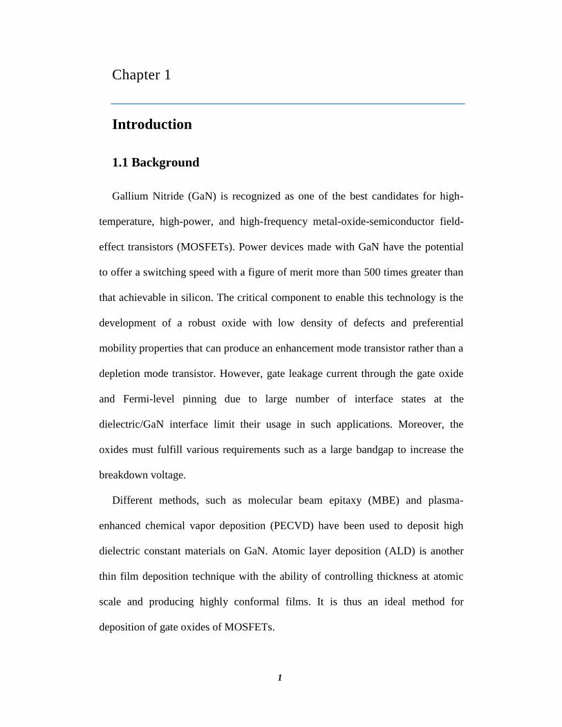
[10]. Both structures have fourfold coordination (see Figure 1.1). The difference
between these two structures is the bond angle of the second-nearest neighbor
[11]. The stacking order in WZ is ABABAB along [0001] direction, but in ZB is
ABCABC along [111] direction. At high pressure, the RC crystal structure is the
stable one [10]. Table 1.1 compares some properties of WZ and ZB GaN.
4
(a) (b)
Figure 1.1 Schematic diagrams of wurtzite (a) and zincblende (b) crystal structures. The
dark, and bright spheres represent nitrogen, and gallium atoms, respectively.
Table 1.1 Some GaN characteristics [12]
Crystal structure Wurtzite Zincblende
Group of Symmetry
Density (g/cm3)
Dielectric constant
Static
High frequency
Lattice constant (Å)
C6vP63mc
6.15
8.9-9.5
5.35
a=3.189, c=5.185
6.15
9.7
5.3
4.52
1.2.3 GaN-Based Transistors
A combination of high current density, high breakdown electric field, and good
thermal conductivity can be found in GaN-based transistors [13]. This allows high
microwave performance for the solid-state transistors. GaN power devices have
the potential to offer a high switching speed and power density with a figure of
merit (FOM) greater than 500 times than that achievable in silicon [10].
Several figures of merit (FOM) have been developed for microwave
transistors: Johnson’s (vsatEc/π) 2, Baliga’s (Ec
2), and Keyes’ FOM ((vsat/r)
0.5)
[13]. Here, Ec is the breakdown electric field, vsat is the electron saturation
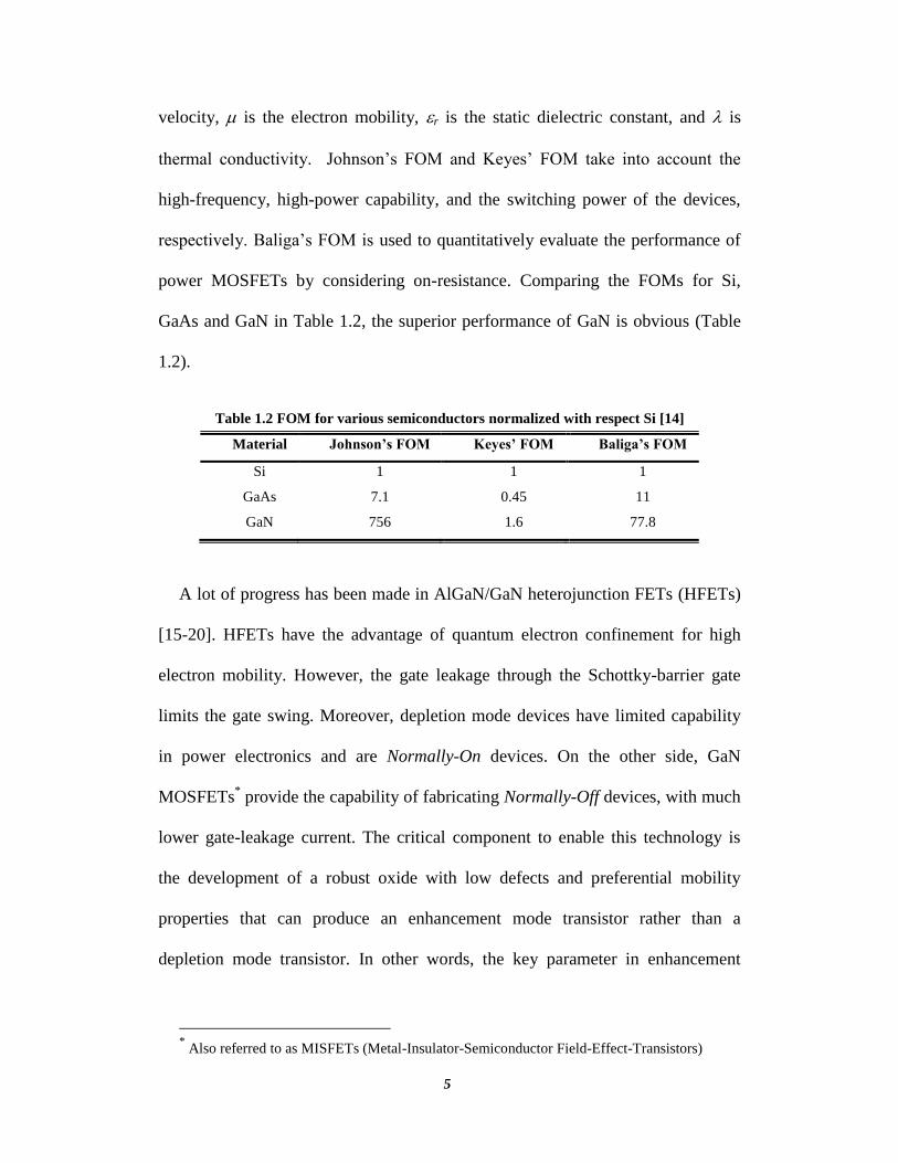
5
velocity, is the electron mobility, r is the static dielectric constant, and is
thermal conductivity. Johnson’s FOM and Keyes’ FOM take into account the
high-frequency, high-power capability, and the switching power of the devices,
respectively. Baliga’s FOM is used to quantitatively evaluate the performance of
power MOSFETs by considering on-resistance. Comparing the FOMs for Si,
GaAs and GaN in Table 1.2, the superior performance of GaN is obvious (Table
1.2).
Table 1.2 FOM for various semiconductors normalized with respect Si [14]
Material Johnson’s FOM Keyes’ FOM Baliga’s FOM
Si
GaAs
GaN
1
7.1
756
1
0.45
1.6
1
11
77.8
A lot of progress has been made in AlGaN/GaN heterojunction FETs (HFETs)
[15-20]. HFETs have the advantage of quantum electron confinement for high
electron mobility. However, the gate leakage through the Schottky-barrier gate
limits the gate swing. Moreover, depletion mode devices have limited capability
in power electronics and are Normally-On devices. On the other side, GaN
MOSFETs* provide the capability of fabricating Normally-Off devices, with much
lower gate-leakage current. The critical component to enable this technology is
the development of a robust oxide with low defects and preferential mobility
properties that can produce an enhancement mode transistor rather than a
depletion mode transistor. In other words, the key parameter in enhancement
* Also referred to as MISFETs (Metal-Insulator-Semiconductor Field-Effect-Transistors)
6
mode transistors is the quality of the gate oxide and its compatibility with
underlying GaN material.
1.2.4 MOSFET Operation and Interface Oxides
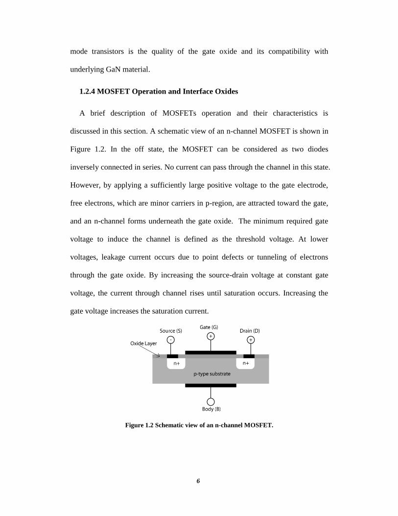
A brief description of MOSFETs operation and their characteristics is
discussed in this section. A schematic view of an n-channel MOSFET is shown in
Figure 1.2. In the off state, the MOSFET can be considered as two diodes
inversely connected in series. No current can pass through the channel in this state.
However, by applying a sufficiently large positive voltage to the gate electrode,
free electrons, which are minor carriers in p-region, are attracted toward the gate,
and an n-channel forms underneath the gate oxide. The minimum required gate
voltage to induce the channel is defined as the threshold voltage. At lower
voltages, leakage current occurs due to point defects or tunneling of electrons
through the gate oxide. By increasing the source-drain voltage at constant gate
voltage, the current through channel rises until saturation occurs. Increasing the
gate voltage increases the saturation current.
Figure 1.2 Schematic view of an n-channel MOSFET.

7
The quality of the gate oxide has a lot of influence on the performance of the
MOSFET. Trapped charges in gate oxide may degrade the electrical performance.
Four types of charges can be found in the gate oxide [21]: (1) Fixed oxide charge,
which is the result of structural defects in oxide layer, but it has no interaction
with the buried semiconductor. Annealing in N2 or Ar atmosphere can eliminate
these defects. (2) Mobile oxide charge, which comes from ionic impurities like
Na+ and Li
+ ions. (3) Oxide trapped charge, which comes from holes and
electrons trapped in bulk oxide due to the ionizing radiation or avalanche injection
of carriers from channel. (4) Interface trapped charge, which is due to structural
defects at the interface of oxide/semiconductor. The latter is in electrical
communication with underlying semiconductor layer and may degrade electrical
performance of the device.
Capacitance-Voltage (C-V) curves measured at different frequencies and
biases are used to determine the density of interface states. Different methods
have been developed for this purpose as discussed in ref. [21]. Interface states also
can affect the threshold voltage or cause increase of leakage current. Carriers can
jump into interface states and then easily tunnel through the gate oxide. This
current is temperature dependent and can be detected through temperature
dependent I-V curves [22].
1.2.5 Gate Oxide Materials for GaN MOSFETs
As mentioned earlier, GaN-based MOSFETs have some major advantages over
Schottky gate devices. Enhancement-mode MOSFETs have a larger voltage
sweep range, lower gate leakage currents, improved thermal stability and higher
8
temperature operation. Moreover, the circuit design process is simpler since they
can be used to form single supply voltage control circuits for power transistors [23,
24]. Moreover, integration of dielectrics can decrease the current collapse by
surface passivation, which is the main obstacle of AlGaN/GaN HFETs [25].
There are two problems with the native oxides of III-V compounds [26]: (1)
since they are binary in nature finding a synthesis method for their formation is
very difficult, and (2) surface atom bonds have formal fractional occupancy. For
example, on the (0001) face in GaN, the formal orbital occupancy for gallium
dangling bond is 3/4 of an electron, and for nitrogen is 5/4 of an electron. As a
result, insulators such as SiO2 and Si3N4 cannot form covalent two electron pair
bonds between the GaN surface atoms without the creation of charged bonding
arrangements. These charged bonds generally degrade interface electronic
properties.
Processes like remote plasma ALD, with separate control over interface
formation and film deposition can promote the charge distribution on GaN surface
and could allow two electrons interfacial bonding between dielectric and GaN
[26]. By replacing the SiO2 with high-κ dielectrics in silicon MOSFETs, silicon
has lost some of its advantages over wide bandgap semiconductors, because the
high-κ dielectrics are not native oxides and can be deposited on any
semiconductor [27].
The key guidelines for selecting a high-κ gate dielectric are [27, 28]:
(1) high permittivity, large bandgap, and sufficient band offset (>1eV)
(2) thermal stability
9
(3) thermodynamic stability in contact with the semiconductor
(4) good passivation and interface quality
(5) compatibility with the current or expected materials to be used in
processing for CMOS devices
(6) process compatibility
(7) reliability.
Many dielectrics meet some of these requirements but very few materials are
favorable with respect to all of the criteria. A summary of these dielectric
materials will be presented after describing heterojunction band alignment.
1.2.6 Heterojunction Band Alignment
The band alignment at the interface of GaN/dielectric has an important
influence on device performance. As mentioned earlier, large valence and
conduction band offsets are required to prevent injection of free electrons and
holes [27].
Based on bandgap and electron affinities, three types of band alignments can
be formed when two materials with bandgaps are in contact [29]: (1) type I, (2)
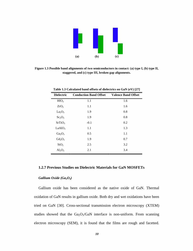
type II, staggered, and (3) type III, broken gap alignments (Figure 1.3). Direct
interaction between semiconductor materials results in space charge redistribution
and leads to band bending near the junction. A nominated dielectric should form
type I band alignment to reduce the leakage currents in MOSFET device. Table
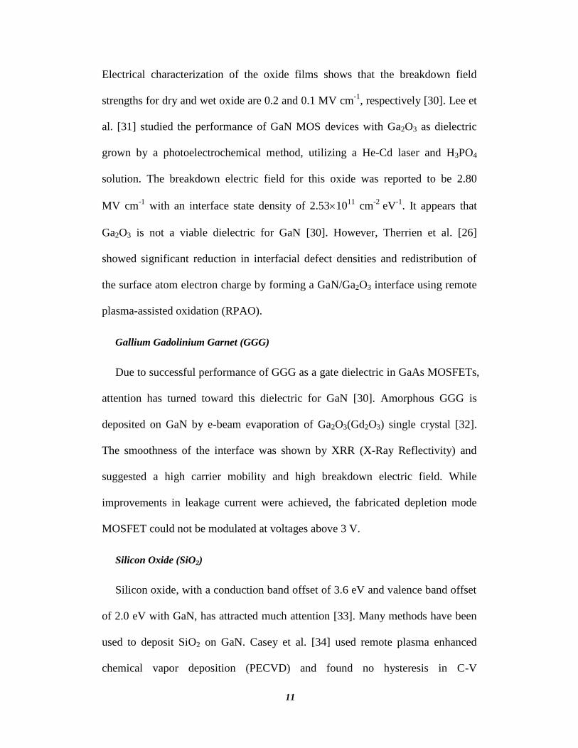
1.3 shows the band alignment of various oxides on GaN.
10
Figure 1.3 Possible band alignments of two semiconductors in contact: (a) type I, (b) type II,
staggered, and (c) type III, broken gap alignments.
Table 1.3 Calculated band offsets of dielectrics on GaN (eV) [27]
Dielectric Conduction Band Offset Valence Band Offset
HfO2
ZrO2
La2O3
Sc2O3
SrTiO3
LaAlO3
Ga2O3
Gd2O3
SiO2
Al2O3
1.1
1.1
1.9
1.9
-0.1
1.1
0.5
1.9
2.5
2.1
1.6
1.6
0.8
0.8
0.2
1.3
1.1
0.7
3.2
3.4
1.2.7 Previous Studies on Dielectric Materials for GaN MOSFETs
Gallium Oxide (Ga2O3)
Gallium oxide has been considered as the native oxide of GaN. Thermal
oxidation of GaN results in gallium oxide. Both dry and wet oxidations have been
tried on GaN [30]. Cross-sectional transmission electron microscopy (XTEM)
studies showed that the Ga2O3/GaN interface is non-uniform. From scanning
electron microscopy (SEM), it is found that the films are rough and facetted.
11
Electrical characterization of the oxide films shows that the breakdown field
strengths for dry and wet oxide are 0.2 and 0.1 MV cm-1
, respectively [30]. Lee et
al. [31] studied the performance of GaN MOS devices with Ga2O3 as dielectric
grown by a photoelectrochemical method, utilizing a He-Cd laser and H3PO4
solution. The breakdown electric field for this oxide was reported to be 2.80
MV cm-1
with an interface state density of 2.531011
cm-2
eV-1
. It appears that
Ga2O3 is not a viable dielectric for GaN [30]. However, Therrien et al. [26]
showed significant reduction in interfacial defect densities and redistribution of
the surface atom electron charge by forming a GaN/Ga2O3 interface using remote
plasma-assisted oxidation (RPAO).
Gallium Gadolinium Garnet (GGG)
Due to successful performance of GGG as a gate dielectric in GaAs MOSFETs,
attention has turned toward this dielectric for GaN [30]. Amorphous GGG is
deposited on GaN by e-beam evaporation of Ga2O3(Gd2O3) single crystal [32].
The smoothness of the interface was shown by XRR (X-Ray Reflectivity) and
suggested a high carrier mobility and high breakdown electric field. While
improvements in leakage current were achieved, the fabricated depletion mode
MOSFET could not be modulated at voltages above 3 V.
Silicon Oxide (SiO2)
Silicon oxide, with a conduction band offset of 3.6 eV and valence band offset
of 2.0 eV with GaN, has attracted much attention [33]. Many methods have been
used to deposit SiO2 on GaN. Casey et al. [34] used remote plasma enhanced
chemical vapor deposition (PECVD) and found no hysteresis in C-V
12
measurements. Sawada et al. [35], using the same deposition method, showed an
interface state density as low as 11011
eV-1
cm-2
. Despite a low interface state
density, SiO2 suffers from a low dielectric constant (3.9) that results in high
leakage current.
Silicon Nitride (Si3N4)
Silicon nitride has been extensively used for the passivation of HFET surfaces.
Silicon nitride deposited on GaN by electron cyclotron resonance assisted plasma
chemical vapor deposition (ECR-PCVD) showed interface state density of
51010
eV-1
cm-2
[36]. However, Si3N4 forms a type II band alignment with GaN
and has a low dielectric constant as 5. As a result, it can only be used as a barrier.
Aluminum Nitride (AlN)
Undopped aluminum nitride with a bandgap of 6.2 eV can act as an insulator.
The dielectric constant is relatively high, 8-9, and hexagonal aluminum nitride has
only 2.4% lattice mismatch with hexagonal gallium nitride on the (0001) plane
[37]. In spite of this, AlN has a tendency to deposit with a polycrystalline
structure. Unlike amorphous dielectrics, single crystal and polycrystalline AlN
films suffer from low breakdown field due to defects and grain boundaries [30].
The AlN deposited by metal-organic molecular beam epitaxy (MOMBE) at
400 C showed a breakdown field of 1.4 MV cm-1
[37].
MgO, and MgCaO Ternary Oxide
MgO has a bandgap of 8 eV and a dielectric constant of 9.8 and hence it is an
alternative gate oxide material for GaN [38]. An interface state density as low as
13
21011
eV-1
cm-2
was achieved for MgO deposited on GaN using elemental Mg
and oxygen plasma [38]. CaO is also a rocksalt dielectric like MgO and has a
dielectric constant of 11.8. Although the lattice constant of MgO is smaller than
GaN, CaO has larger lattice constant [30]. A ternary oxide consisting of MgO and
CaO could thus be closely matched to GaN. Mg0.5Ca0.5O was found to have the
same atomic spacing on (111) plane as GaN [30]. The problem with this material
system is that Mg and Ca are immiscible due to the large difference in atomic
diameter between Mg and Ca and the film is unstable. Capping the film with
stable oxides such as Sc2O3 can overcome this degradation [39].
Rare Earth Oxides
Rare earth elements are extremely reactive with oxygen and form very stable
oxides. Their cubic and hexagonal phases are interesting as gate oxides for GaN
MOSFETs [22]. The rare earth oxides with smaller ionic radii crystallize in the
bixbyite structure. The bixbyite crystal structure exhibits similar atomic symmetry
in the (111) plane as the GaN (0001), so they could be grown epitaxially on GaN.
Another interesting feature of rare earth oxides is their large bandgap, close to
6 eV, and the large band offsets with GaN [22]. The dielectric constant of these
oxides is relatively very high ( = 7 - 20).
Gadolinium oxide (Gd2O3) is an attractive oxide because of high dielectric
constant, 11.4, and a bandgap of 5.3 eV [30]. However, the bond length mismatch
between Gd2O3 (111) and GaN (0001) is about 20% [30]. As a consequence, the
dislocations created in the film limit the breakdown field by acting as current
leakage paths. Johnson et al. [40] showed that the formation of the stacked gate
14
dielectric of SiO2/Gd2O3 could terminate the formation of the dislocations in the
crystalline oxides. The high melting point of these materials suggests high thermal
stability.
Scandium Oxide (Sc2O3) has a much smaller lattice constant than Gd2O3
(9.2% mismatch to GaN), which should make it less defective when deposited on
GaN [30]. It has a bandgap of 6.3 eV and a dielectric constant of 14 [30]. Sc2O3
has been grown epitaxially on GaN using MBE [41]. The results showed that a
GaOx passivation layer is needed to allow for a suitable growth of the epitaxial
oxide on GaN and to achieve low leakage current densities. From the I–V and C–
V data, a forward breakdown field of 0.7 MV cm-1
and an interface state density
41011
eV-1
cm-2
were calculated [42]. Lanthanum Oxide (La2O3) is also among
the rare earth oxides deposited on GaN [30, 43, 44]. However, the rare earth
oxides are hygroscopic [22]. They become hydrated and carbonated in contact
with atmosphere at ambient pressure and temperature. In fact, the OH- can easily
bond to the rare earth atom. Hydroxide contamination results in degradation of the
dielectric constant [22].
Aluminum Oxide (Al2O3)
Al2O3 is attractive due to its large bandgap, 9 eV, and high breakdown field,
~10 MV cm-1
[23, 45, 46]. To date MBE [47] and MOCVD [48] have been used
to deposit alumina on GaN. One of the advantages of Al2O3 is that it can easily be
deposited using atomic layer deposition (ALD) and hence it can have all the
advantages of ALD, which are discussed in next section. For example, Ye et al.
[45] deposited alumina on GaN using ALD at 300 C. The midgap interface trap
15
density was found to be 1011
– 1012
eV-1
cm-2
. Wu et al. [49] made a GaN
MOSFET with ALD Al2O3 as its gate oxide and measured a leakage current less
than 10-6
mA mm-1
at a gate voltage of 4V, one order of magnitude less than that
of Gd2O3. Using remote-plasma ALD, Yun et al. [46] achieved a MOS structure
with a leakage current density as low as 10-10
A cm-2
at 1MV cm-1
and an
interface state density about 1.21011
eV-1
cm-2
. Compared to rare earth oxides,
however, the dielectric constant of alumina, ~ 9, is low.
The properties of the different dielectric materials used as the gate oxide of the
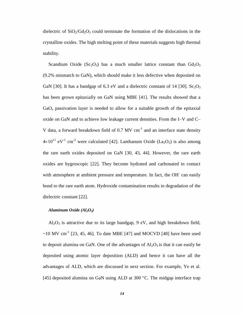
GaN MOSFETs are summarized in table 1.4.
Table 1.4 A summary of some of the properties of dielectric materials used as the gate oxide
of the GaN MOSFETs
Material Bandgap
(eV)
Dielectric
Constant
Breakdown voltage
(MV cm-1
)
Defect Density
(eV-1
cm-2
)
Mismatch
to GaN (%)
Ga2O3
SiO2
Si3N4
AlN
MgO
Gd2O3
Sc2O3
Al2O3
5
9
5
6.2
8
5.3
6.3
9
10
3.9
5
8 – 9
9.8
11.4
14
9
0.1 – 2.8
-
-
1.4
-
-
0.7
1-10
2.531011
11011
51010
-
21011
-
41011
1011
-1012
-
-
-
2.4
-
20
9.2
-
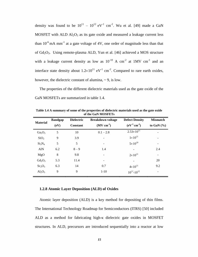
1.2.8 Atomic Layer Deposition (ALD) of Oxides
Atomic layer deposition (ALD) is a key method for depositing of thin films.
The International Technology Roadmap for Semiconductors (ITRS) [50] included
ALD as a method for fabricating high-κ dielectric gate oxides in MOSFET
structures. In ALD, precursors are introduced sequentially into a reactor at low
16
pressures, ~1 torr. Each reactant pulse is followed by a purge step to sweep out
the excess reactants and byproducts (See Figure 1.4). ALD is a self-limiting
process with a subnanometer control over thickness of layers, with uniform and
conformal thin films.
Figure 1.4 Schematic representation of an ALD cycle.
Conformality is a key characteristic because unlike the traditional
semiconductor technology, the basic building blocks for nanotechnology are not
limited to planar type substrates [51]. Another characteristic of ALD is its control
over thickness and composition [51]. This makes ALD an ideal technique for
depositing high-κ dielectrics gate oxides for MOSFET applications. The other
feature of ALD is that it is fundamentally a low-temperature deposition technique
[51]. For example, ALD of Al2O3 at 33 C has been reported by Groner et al. [52].
This feature is more important for depositing polymers and low-k dielectric
materials.
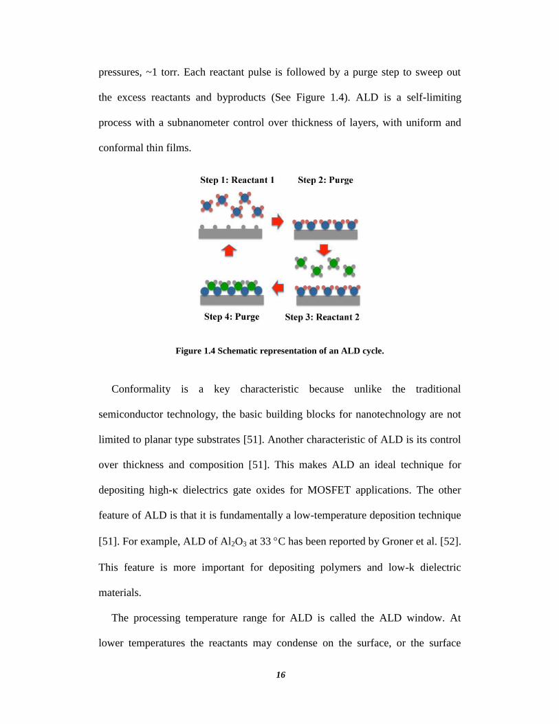
The processing temperature range for ALD is called the ALD window. At
lower temperatures the reactants may condense on the surface, or the surface
17
reactions may not have enough thermal energy to proceed [53]. At higher
temperatures decomposition or desorption of surface species occurs and the
growth rate decreases [53]. A schematic of the ALD window has shown in Figure
1.5.
Figure 1.5 Schematic of ALD window and possible behavior of ALD growth.
With utilization of ALD in large-scale production for Si-based integrated
circuits, attention has been attracted to using ALD for depositing high-κ
dielectrics on Ge and III-V materials [54]. The native oxide on the surface of
III-V semiconductors has a significant impact on the interface state density and
results in poor device performance due to Fermi level pinning [54].
Al2O3, HfO2, and HfAlO (Al2O3/HfO2) are among the gate oxide materials
deposited by ALD on III-V semiconductors [54]. A lot of progress has been made
in understanding the effect of the chemistry of the oxide/semiconductor interface
on electrical performance such as Fermi level pinning and the nature of the
associated defect states [54]. However, more effort is needed to enable the
realization of high-performance MOSFETs using III-V semiconductors. An
18
introduction and a literature review of ALD of ZrO2 and HfO2 are discussed in
Chapters 5 and 6, respectively.
1.3 Objectives of This Work
In the last decade, ALD has recently been recognized as an ideal tool for
depositing high-κ materials on silicon. However, few studies have been done on
ALD of high-κ dielectrics on GaN. HfO2 and ZrO2 are two promising high-κ
materials, which have rarely been studied for the application as a gate oxide of
GaN and ZnO. A fundamental understanding of the nucleation and growth
mechanisms is required to control the quality of the ALD oxides and developing
new applications. Meanwhile, there is a lack of a systematic study on growth
mechanisms and characteristics of HfO2 and ZrO2 as well as ZnO thin films
deposited by ALD. Two different approaches were used to tackle this problem. In
the first approach, different analytical tools including X-ray diffraction (XRD), X-
ray photoelectron spectroscopy (XPS), atomic force microscopy (AFM),
transmission electron microscopy (TEM), in-situ spectroscopy ellipsometry, Hall
mobility and four-point probe techniques were used to investigate the HfO2, ZrO2,
and ZnO thin films properties. The growth models were proposed for ALD of the
oxide based on the experimental results. In the second approach, density
functional theory (DFT) was utilized to explore the reaction pathways between the
precursor molecules and the oxide surface, and to compute the thermodynamic
stability of intermediate states and activation energies of various reactions at the
deposition temperature and pressure. Finally, metal-oxide-semiconductor
capacitors (MOSCAPs) were fabricated and capacitance-voltage (C-V)
19
measurements were performed on the structure to study the quality of the
interface between the semiconductor and high-κ oxides.
1.4 Outline of Thesis
An introduction on ALD, GaN, ZnO, and the high-κ oxides was presented in
this chapter. The objective and the roadmap to tackle the problems were offered
as well. Chapter 2 is a brief introduction to the quantum chemical modeling and
density functional theory, which are utilized in chapters 4-6 to study the reaction
pathways of the ALD oxides. Chapter 3 outlines the experimental procedure and
techniques used to explore the ALD oxides. Chapter 4, 5, and 6 discuss a
thorough and comprehensive study on characterization of structure, morphology,
and chemistry of ZnO, ZrO2, and HfO2 deposited by thermal and plasma-
enhanced ALD methods. Chapter 7 introduces the novel method for investigation
of nucleation and growth mechanism of ALD oxides utilizing in-situ
spectroscopic ellipsometry. The overall conclusion of this work is summarized in
Chapter 8, along with suggestions for future work.
20
Chapter 2
Theoretical Background of Quantum Chemistry
Calculations
In the early twentieth century, physicists discovered that Newton’s classical
mechanics did not properly describe the behavior of a system containing very
small particles. The groundbreaking contributions of Planck, Einstein, Bohr,
Heisenberg, Born, Jordan, Pauli, Fermi, Schrödinger, Dirac, de Broglie and Bose
led to discovery of quantum mechanics, which described the behavior of such
systems. Pauling, Hartree, Fock, Slater, Thomas, Fermi, Bloch, Dirac, Wigner,
and Mulliken applied quantum mechanics to the problems in chemistry and laid
the foundation of modern computational quantum chemistry.
This chapter provides an introductory summary to the theory underlying
computational chemistry. The emphasis is on the molecular electronic structure,
energetic, geometry and vibrational calculations. More detailed knowledge of
quantum chemistry can be found in “Quantum Chemistry” by Levin [55].
2.1 Schrödinger Equation for a Many-Body System
To describe the state of a system in quantum mechanics, we have to find the
state function or wave function, Ψ(r, t), of that system. Ψ(r, t) is a function of the
coordinates of the particles in the system and time, and contains all the possible
information about the system. The fundamental equation of quantum chemistry is
the Schrödinger wave equation or time-dependent Schrödinger equation.
21
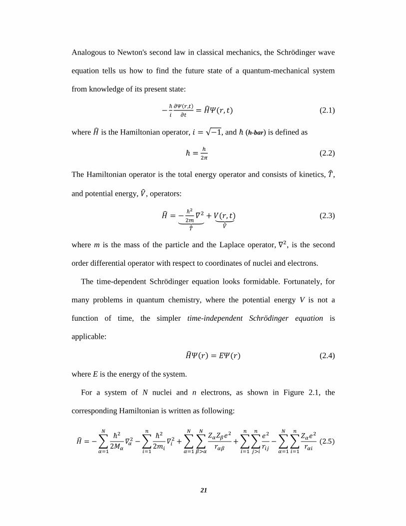
Analogous to Newton's second law in classical mechanics, the Schrödinger wave
equation tells us how to find the future state of a quantum-mechanical system
from knowledge of its present state:
(2.1)
where is the Hamiltonian operator, , and (h-bar) is defined as
(2.2)
The Hamiltonian operator is the total energy operator and consists of kinetics, ,
and potential energy, , operators:
(2.3)
where m is the mass of the particle and the Laplace operator, , is the second
order differential operator with respect to coordinates of nuclei and electrons.
The time-dependent Schrödinger equation looks formidable. Fortunately, for
many problems in quantum chemistry, where the potential energy V is not a
function of time, the simpler time-independent Schrödinger equation is
applicable:
(2.4)
where E is the energy of the system.
For a system of N nuclei and n electrons, as shown in Figure 2.1, the
corresponding Hamiltonian is written as following:
22
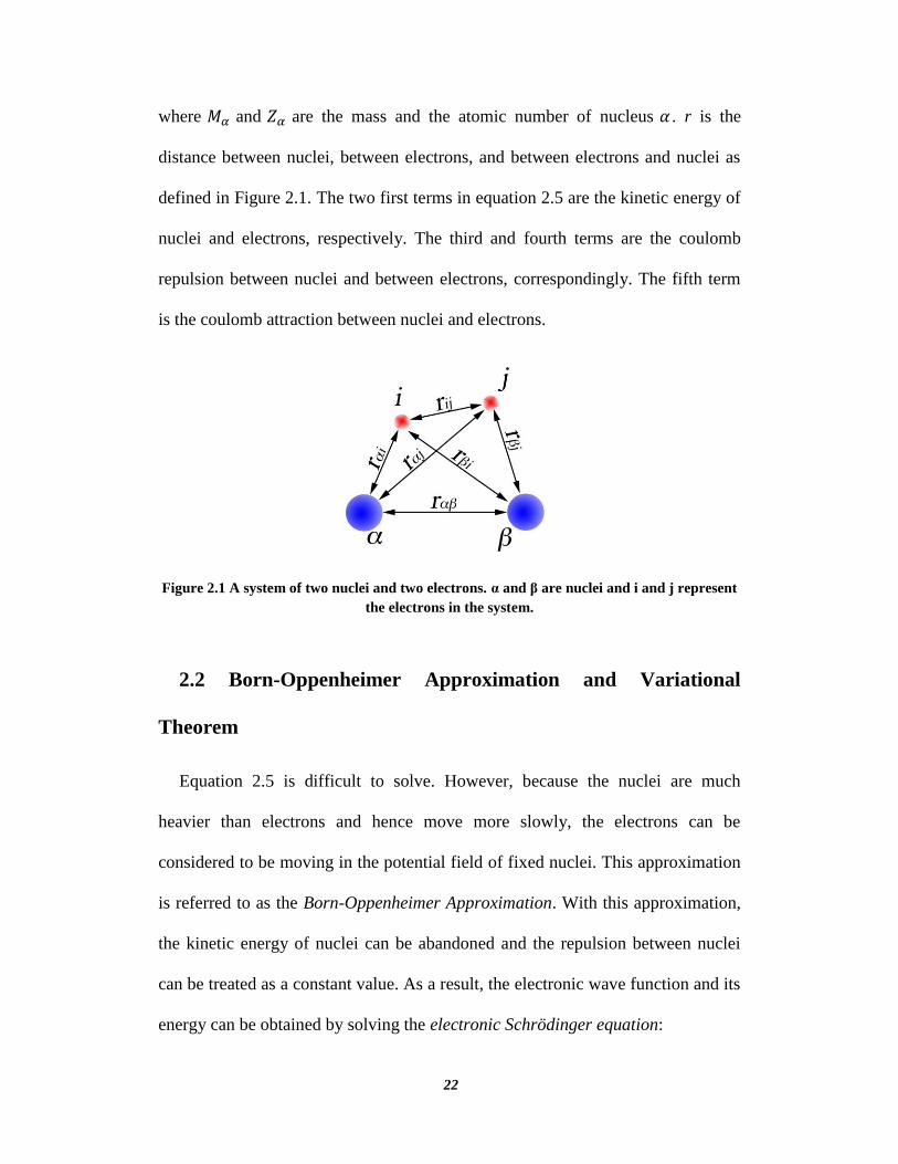
where and are the mass and the atomic number of nucleus . r is the
distance between nuclei, between electrons, and between electrons and nuclei as
defined in Figure 2.1. The two first terms in equation 2.5 are the kinetic energy of
nuclei and electrons, respectively. The third and fourth terms are the coulomb
repulsion between nuclei and between electrons, correspondingly. The fifth term
is the coulomb attraction between nuclei and electrons.
Figure 2.1 A system of two nuclei and two electrons. α and β are nuclei and i and j represent
the electrons in the system.
2.2 Born-Oppenheimer Approximation and Variational
Theorem
Equation 2.5 is difficult to solve. However, because the nuclei are much
heavier than electrons and hence move more slowly, the electrons can be
considered to be moving in the potential field of fixed nuclei. This approximation
is referred to as the Born-Oppenheimer Approximation. With this approximation,
the kinetic energy of nuclei can be abandoned and the repulsion between nuclei
can be treated as a constant value. As a result, the electronic wave function and its
energy can be obtained by solving the electronic Schrödinger equation:
23
(2.6)
where the electronic Hamiltonian, , is
Solving the electronic Schrödinger equation is still a challenging task.
However, we can make approximate solutions by employing the variational
theorem. The variational theorem states that any approximate wave function has
an energy that is above or equal to that of the exact wave function energy and the
equality stands for the exact solution. Practically, a trial wave function is chosen
and then the variational theorem is used to indicate accuracy of the trial: the lower
the calculation energy, the closer the trial wave function to the real solution.
The common approach is to construct a trial wave function as a linear
combination of basis functions, φi,
(2.8)
The task is to find the optimum set of basis function coefficient, {ci}, which gives
the lowest possible energy.
2.3 Basis Functions
Two most common basis functions are Slater-type functions and Gaussian-type
functions. The Slater-type has the form of
(2.9)
and the Gaussian-type function has the form of
(2.10)
24
ζ and α are Slater and Gaussian orbital exponents. The orbital exponents
determine the diffuseness of the basis functions. A small exponent results in a
large dense function. The differences between these two type of basis functions
occur at r = RA, where the Gaussian function has a slope of zero while the Slater
functions has a finite slope. Moreover, at large values of the Gaussian
function falls off more rapidly. In spite of Slater functions, which can only be
computed numerically, the integral over Gaussian functions can be solved
analytically and this means much faster calculations. However, it is worthy to
mention that the exact solution to the Schrödinger equation for the hydrogen atom
is a Slater-type orbital (STO). For a better description of the shape of molecular
orbitals using the Gaussian functions, a linear combination of the primitive
functions are used to construct a contracted Gaussian function.
Larger basis sets describe molecule orbitals better as they enforce fewer
restrictions on the location of the electrons in space. One method is to use more
than one basis set to describe each valence orbital. These sets of functions are
called split valence basis sets. Adding polarization functions, with higher angular
momentum, and diffuse functions, which allows orbitals to span a larger space, are
other ways to improve the basis functions. For the atoms beyond the third row of
periodic table, it is common to use effective core potentials (ECP). The ECP
describes the electrons near the nucleus while the Gaussian basis functions depicts
the valence electrons.
Basis sets denoted by the general nomenclature N-M1G or N-M11G, where N
and M are integers. The G in the name simply indicates the Gaussian basis
25
functions. The N-M1G is a split valence double zeta basis set while the N-M11G
is a split valence triple zeta basis set. As an example, in the split valence double
zeta basis set 6-31+G(d,p) basis set for carbon atom, N=6 represents the number
of the Gaussian functions to describe the core orbital, 1s. M=3 indicates the
number of Gaussian primitives to describe 2s and 2p orbitals. The “1” means one
Gaussian primitive is used to define the 2s’ and 2p’ basis functions. (d,p) shows
that one set of d-type polarization functions is added to all non-hydrogen atoms
and one set of p-type polarization functions is added to hydrogen atoms. The +
sign means that one set of sp-type diffuse basis functions is added to non-
hydrogen atoms. To summarize this example, the 6-31+G(d,p) basis set for carbon
contains 19 basis functions and 32 primitive functions:
1s (6 primitives)
2s, 2p, 2p, 2p (4×3=12 primitives)
2s’, 2p’, 2p’, 2p’(4×1=4 primitives)
3d, 3d, 3d, 3d, 3d, 3d (6×1=6 primitives)
2s+, 2p+, 2p+, 2p+ (4×1=4 primitives)
2.4 Molecular Orbital Methods – Hartree-Fock
Solving the Schrödinger equation for a molecule is a many-body problem and
is difficult to solve. The Hamiltonian depends on the wave function and vice versa
because of the two-electron repulsion term. The simplest approach is to overlook
this term. In this case, similar to the total probability of the independent events,
the wave function of the non-interacting electrons is the product of each single
electron wave function, which is called the Hartree product. However, the
26
Hartree product does not satisfy the antisymmetry principle. The antisymmetry
principle states that the wave function changes sign with respect to the
interchange of any two electrons.
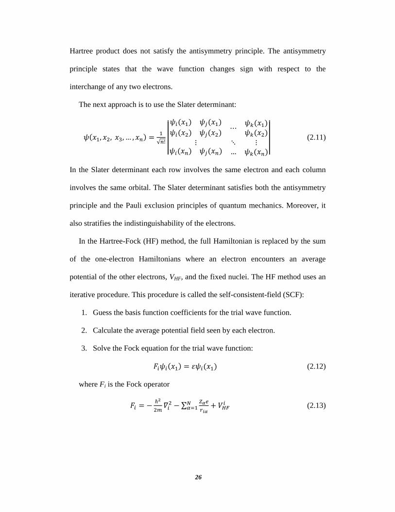
The next approach is to use the Slater determinant:
(2.11)
In the Slater determinant each row involves the same electron and each column
involves the same orbital. The Slater determinant satisfies both the antisymmetry
principle and the Pauli exclusion principles of quantum mechanics. Moreover, it
also stratifies the indistinguishability of the electrons.
In the Hartree-Fock (HF) method, the full Hamiltonian is replaced by the sum
of the one-electron Hamiltonians where an electron encounters an average
potential of the other electrons, VHF, and the fixed nuclei. The HF method uses an
iterative procedure. This procedure is called the self-consistent-field (SCF):
1. Guess the basis function coefficients for the trial wave function.
2. Calculate the average potential field seen by each electron.
3. Solve the Fock equation for the trial wave function:
(2.12)
where Fi is the Fock operator
(2.13)
27
4. Minimize the expectation value of the Fock operator, Fi, with respect to
the basis set coefficients and construct a new set of orbitals and new trial
wave function.
5. Calculate the new VHF from the new trial function and repeat steps 3 and 4
until the potential field and the wave function do not change.
The HF method neglects electron correlation and this can cause a large
deviation from the exact solution. Modern methods are implemented to account
for the correlation and coupling effects. These methods are categorized as post-
HF methods. More description of these methods can be found in quantum
chemistry textbooks [55].
2.5 Density Functional Theory
Unlike the HF and post-HF methods, density functional theory (DFT) does not
calculate the wave function of the electrons. DFT is based on two theorems,
known as the Hohenberg-Kohn theorems [56]:
“1. Knowing the ground-state density, , it is possible to drive the
corresponding wave function. It means that the ground-state wave function is a
functional of electron density, .
2. The electron density that minimizes the energy of the overall functional is
the exact electron density corresponding to the full solution of the Schrödinger’s
equation.”
Unfortunately, the Hohenberg-Kohn theorems do not describe how to find the
electron density, or how to calculate the energy from the electron density. This
was done by Kohn and Sham in 1965 [57].
28
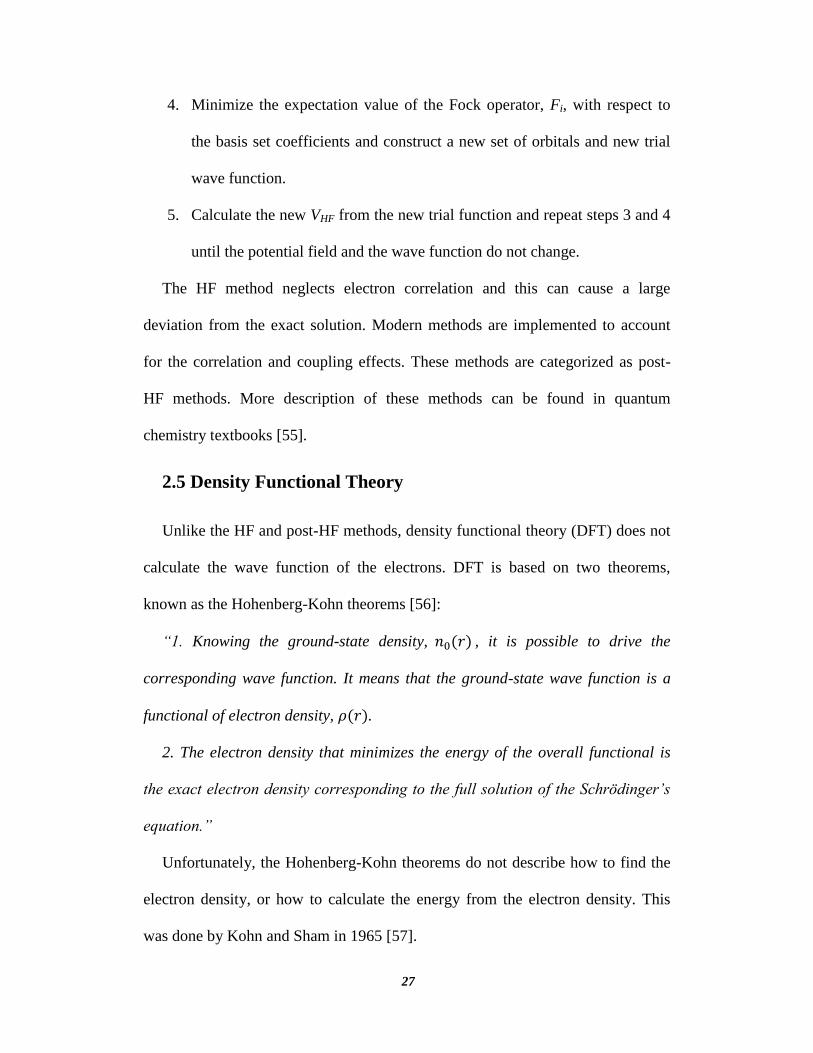
The energy of the system, EKS, can be written as:
(2.14)
where T is the electronic kinetic energy, Ve-n is the electronic potential energy
from attraction of electrons and nuclei, Ve-e is the electronic potential from
repulsion of electrons, and Exc is the exchange-correlation energy.
To determine the energy, the Kohn-Sham equation has to be solved using the
variational principle:
(2.15)
where is the Kahn-Sham orbital. The electronic density is calculated using:
(2.16)
and the exchange-correlation potential, Vxc, is found using:
(2.17)
The only unknown is the exchange-correlation energy functional. The
improvements in Exc lead to improvement in the calculated properties and energy
of the system under study.
Local density approximation (LDA) assumes a uniform electron gas of the
same density in the molecule [58]. However, in real molecules the electron gas is
not uniform. This resulted in the introduction of the generalized gradient
approximation (GGA) that involves the gradient corrections.
Another method, known as Hybrid DFT, involves the combination of
exchange-correlation functional from DFT approaches and HF method. The well-
known B3LYP [59-62] method, the most popular DFT method, is an example of
this approach.
29
2.6 Geometry Optimization and Frequency Calculations
To find the stable or transition structure of the molecules, the stationary points
on the potential energy surface (PES) must be found. This is done by performing
the geometry optimization. PES relates the energy of the system to its molecular
configuration, or the nuclei positions. The stable configuration and the transition
state are considered as the minimum and the first saddle point, respectively. At
both of these configurations the first derivative of energy, which is proportional to
the force, is zero. A geometry optimization begins with finding the electronic
structure of molecular structure. Then, the gradient of the PES is calculated. The
later determines the direction to a stationary point on the PES, which is the new
structure. The energy and forces are calculated for this new structure and the
procedure repeats until:
1. The maximum force is less than a maximum value.
2. The root mean square (RMS) of the forces is less than a maximum value.
3. The maximum displacement is less than a maximum value.
4. The root mean square (RMS) of the displacements is less than a
maximum value.
At this final structure the vibrational frequencies are computed by taking the
second-derivative of the energy with respect to the nuclei positions. For the
stationary point, all the frequencies must be real. However, for the transition
structure, there must be exactly one imaginary frequency [63].
30
2.7 Computational Chemistry Approach to Atomic Layer
Deposition
Computational Chemistry has been used to model ALD chemistry of different
oxides, and nitrides. From these studies the activation energies of the ALD half-
reactions have been computed and the most probable reaction pathways have been
found. These data can be used to design new precursors and to provide validation
for models. A review on the existing papers in this topic is published by Elliott
[64].
Simulation of the ALD reactions can be classified into two categories:
homodeposition or product-on-product, and heterodeposition or product-on-
substrate. The homodeposition refers to the steady-state part of the ALD where
the growth rate is constant. The aim of these studies is to find the desirable and
undesirable reaction pathways. These data provide to understanding on how the
surface reaction sites are consumed and to find the stability of the intermediate
complexes formed during ALD half-reactions. Quantitative answers can lead to
prediction of growth rate, and its dependence on temperature and dose/purge
times.
On the other hand, the heterodeposition refers to the stage where the reactions
are between the substrate, for example Si(100) surface, and the ALD precursors.
The results of these simulations have been used to determine the influence of
reaction site chemistry, for example –H terminated vs. –OH terminated, to control
the interface at atomic levels, and to observe the cleaning effect of the precursors.
31
2.8 Computational Method in This Thesis
Computational chemistry calculations have been performed to aid
interpretation of the experimental results. The homodeposition of zinc oxide,
zirconium oxide, and hafnium oxide was studied by employing the cluster
approximation to represent the oxide surface on which the reactions occur. The
cluster approximations are explained later in the appropriate sections.
GAUSSIAN 09 was used to perform molecular orbital calculations. The geometry
of stationary points was located using the B3LYP gradient corrected density
functional method. 6-311G(d) and 6-31+G(d,p) basis sets were used to describe
the Zn, O, N, C, and H atoms. The LanL2DZ ECP basis set was used for Hf and
Zr atoms. The tight optimization convergence criteria (OPT=TIGHT) and
ultrafine grid (INT=ULTRAFINE) were used for calculations in ZrO2 and HfO2
systems. The frequency calculations were carried out at the same level of theory
to identify the nature of the stationary points (local minima and transition states)
and to calculate the zero-point energy corrections, and the thermal corrections at
ALD temperature and pressure. All energies reported were corrected by the zero-
point energy correction value. To be consistent with the most the literature cited
in this thesis, we used "kcal/mol" unit to report the calculated energies. In order to
test the validity of the calculations, the results were compared with available
experimental data whenever possible.
32
Chapter 3
Experimental Procedures
This chapter presents the methods used to prepare and characterize the samples
using fabricated with ALD. The detailed descriptions of the ALD system and the
characterization methods utilized to quantify the samples are also discussed.
3.1 ALD Reactor
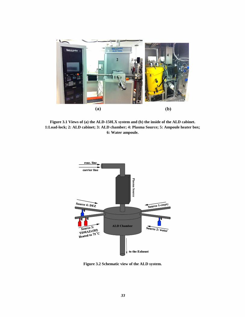
All ALD samples were deposited in an ALD-150LX from Kurt J. Lesker
Company. This reactor is capable of thermal and plasma-enhanced ALD. A
picture of the reactor is shown in Figure 3.1. The samples were loaded into a load-
lock connected to the ALD chamber. The load-lock was then evacuated to 10-7
torr of vacuum to protect the ALD chamber from contamination.
A schematic view of the ALD is shown in Figure 3.2. The use of high-speed
valves in ALD-150LX reactor let the most efficient use of the precursors, with a
dose time as low as 20 ms. Inert gases, Ar or N2, always flow in the reaction lines
to prevent any backflow of the precursors or byproducts from the chamber. The
ALD ampoules are heated to provide sufficient vapor pressure of the precursors, if
required. During the dose time, the ALD mass flow control (MFC) valves open
for a specific time and the Ar flow delivers the precursor vapor to the showerhead
in the main chamber.
33
Figure 3.1 Views of (a) the ALD-150LX system and (b) the inside of the ALD cabinet.
1:Load-lock; 2: ALD cabinet; 3: ALD chamber; 4: Plasma Source; 5: Ampoule heater box;
6: Water ampoule.
Figure 3.2 Schematic view of the ALD system.
34
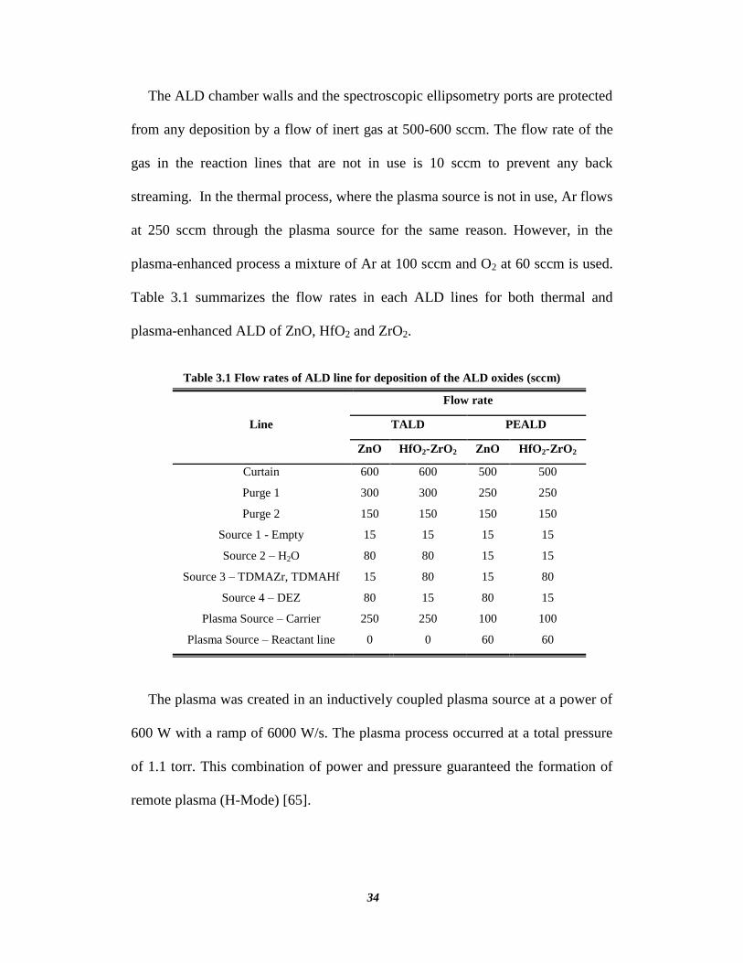
The ALD chamber walls and the spectroscopic ellipsometry ports are protected
from any deposition by a flow of inert gas at 500-600 sccm. The flow rate of the
gas in the reaction lines that are not in use is 10 sccm to prevent any back
streaming. In the thermal process, where the plasma source is not in use, Ar flows
at 250 sccm through the plasma source for the same reason. However, in the
plasma-enhanced process a mixture of Ar at 100 sccm and O2 at 60 sccm is used.
Table 3.1 summarizes the flow rates in each ALD lines for both thermal and
plasma-enhanced ALD of ZnO, HfO2 and ZrO2.
Table 3.1 Flow rates of ALD line for deposition of the ALD oxides (sccm)
Line
Flow rate
TALD PEALD
ZnO HfO2-ZrO2 ZnO HfO2-ZrO2
Curtain
Purge 1
Purge 2
Source 1 - Empty
Source 2 – H2O
Source 3 – TDMAZr, TDMAHf
Source 4 – DEZ
Plasma Source – Carrier
Plasma Source – Reactant line
600
300
150
15
80
15
80
250
0
600
300
150
15
80
80
15
250
0
500
250
150
15
15
15
80
100
60
500
250
150
15
15
80
15
100
60
The plasma was created in an inductively coupled plasma source at a power of
600 W with a ramp of 6000 W/s. The plasma process occurred at a total pressure
of 1.1 torr. This combination of power and pressure guaranteed the formation of
remote plasma (H-Mode) [65].
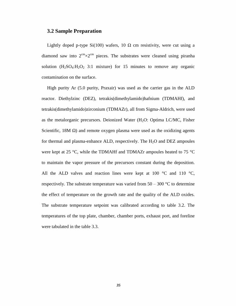
35
3.2 Sample Preparation
Lightly doped p-type Si(100) wafers, 10 Ω cm resistivity, were cut using a
diamond saw into 2cm
×2cm
pieces. The substrates were cleaned using piranha
solution (H2SO4:H2O2 3:1 mixture) for 15 minutes to remove any organic
contamination on the surface.
High purity Ar (5.0 purity, Praxair) was used as the carrier gas in the ALD
reactor. Diethylzinc (DEZ), tetrakis(dimethylamido)hafnium (TDMAHf), and
tetrakis(dimethylamido)zirconium (TDMAZr), all from Sigma-Aldrich, were used
as the metalorganic precursors. Deionized Water (H2O: Optima LC/MC, Fisher
Scientific, 18M Ω) and remote oxygen plasma were used as the oxidizing agents
for thermal and plasma-enhance ALD, respectively. The H2O and DEZ ampoules
were kept at 25 °C, while the TDMAHf and TDMAZr ampoules heated to 75 °C
to maintain the vapor pressure of the precursors constant during the deposition.
All the ALD valves and reaction lines were kept at 100 °C and 110 °C,
respectively. The substrate temperature was varied from 50 – 300 °C to determine
the effect of temperature on the growth rate and the quality of the ALD oxides.
The substrate temperature setpoint was calibrated according to table 3.2. The
temperatures of the top plate, chamber, chamber ports, exhaust port, and foreline
were tabulated in the table 3.3.
36
Table 3.2 Calibration table for the setpoint of the substrate temperature
Setpoint (°C) Substrate Temperature (°C)
55
107
158
210
266
328
50
100
150
200
250
300
Table 3.3 The temperature of the various parts of the ALD system during the deposition
ALD Part Substrate Temperature (°C)
50 100 ≥ 150
Top Plate
Chamber
Chamber Ports
Exhaust Port
Foreline
35
45
45
45
55
87
97
97
97
107
120
130
130
130
140
The T(P)-Mm-TTT format is used to name the samples in this thesis. T or P
specifies if the sample is deposited using TALD or PEALD process. Mm is the
metal in the oxide (Zn:ZnO, Zr:ZrO2, and Hf:HfO2), and TTT is the deposition
temperature.
3.3 In-Situ Spectroscopic Ellipsometry
Spectroscopic ellipsometry (SE) is an optical technique that enables
determination of the thickness and optical properties of thin films. SE measures
the change in polarization of monochromatic polarized light reflected from the
material under study and converts the data into two parameters: the amplitude
ratio, Ψ, and the phase change, Δ.
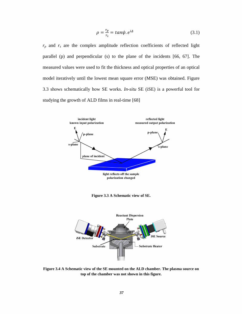
37
(3.1)
rp and rs are the complex amplitude reflection coefficients of reflected light
parallel (p) and perpendicular (s) to the plane of the incidents [66, 67]. The
measured values were used to fit the thickness and optical properties of an optical
model iteratively until the lowest mean square error (MSE) was obtained. Figure
3.3 shows schematically how SE works. In-situ SE (iSE) is a powerful tool for
studying the growth of ALD films in real-time [68]
Figure 3.3 A Schematic view of SE.
Figure 3.4 A Schematic view of the SE mounted on the ALD chamber. The plasma source on
top of the chamber was not shown in this figure.
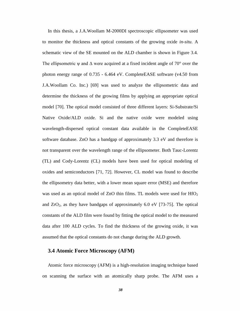
38
In this thesis, a J.A.Woollam M-2000DI spectroscopic ellipsometer was used
to monitor the thickness and optical constants of the growing oxide in-situ. A
schematic view of the SE mounted on the ALD chamber is shown in Figure 3.4.
The ellipsometric ψ and Δ were acquired at a fixed incident angle of 70° over the
photon energy range of 0.735 - 6.464 eV. CompleteEASE software (v4.50 from
J.A.Woollam Co. Inc.) [69] was used to analyze the ellipsometric data and
determine the thickness of the growing films by applying an appropriate optical
model [70]. The optical model consisted of three different layers: Si-Substrate/Si
Native Oxide/ALD oxide. Si and the native oxide were modeled using
wavelength-dispersed optical constant data available in the CompleteEASE
software database. ZnO has a bandgap of approximately 3.3 eV and therefore is
not transparent over the wavelength range of the ellipsometer. Both Tauc-Lorentz
(TL) and Cody-Lorentz (CL) models have been used for optical modeling of
oxides and semiconductors [71, 72]. However, CL model was found to describe
the ellipsometry data better, with a lower mean square error (MSE) and therefore
was used as an optical model of ZnO thin films. TL models were used for HfO2
and ZrO2, as they have bandgaps of approximately 6.0 eV [73-75]. The optical
constants of the ALD film were found by fitting the optical model to the measured
data after 100 ALD cycles. To find the thickness of the growing oxide, it was
assumed that the optical constants do not change during the ALD growth.
3.4 Atomic Force Microscopy (AFM)
Atomic force microscopy (AFM) is a high-resolution imaging technique based
on scanning the surface with an atomically sharp probe. The AFM uses a
39
microfabricated cantilever to scan the surface. A laser reflected off the cantilever
monitors the deflection, or the oscillation amplitude of the cantilever due to the
change in the atomic force between the tip and the surface. A feedback-controlled
piezoscanner adjusts the detected changes in deflection or amplitude to a setpoint
value by actuating the cantilever in Z-direction. The lateral resolution of AFM is
limited by the sharpness of the tip, which is on the order of few nanometers. New
probes offer a typical tip radius of curvature of less than 8 nm. However, the
resolution in Z direction is restricted by the electronic or thermal vibrations and is
on the order of an Angstrom [76].
In this study, A Veeco Dimension 3100 Atomic Force Microscope was used to
study the roughness and to characterize the quality of the ALD films. The AFM
instrument was located on a structurally isolated floor pad on an air table to
minimize any vibration from the surrounding environment. All measurements
were taken in tapping mode using NanoWorld Pointprobe® NCH probes with a
force constant of 42 N/m and a resonance frequency of 320 kHz. Scans were
made from a 1.0×1.0 μm2 area with a scan rate of 1 Hz and a resolution of 512
lines in both X and Y direction. All the AFM studies were performed on 20nm-
thick films.
After obtaining the AFM images, they were subjected to 3rd
order flattening
using the NanoScope Analysis v1.40r1 software to remove any nonlinear
background artifacts due to the piezoscanner. Three different roughness
parameters were calculated:
(3.2)
40
(3.3)
(3.4)
where Zj is the height of the profile at point j, N is the number of the points, Ra is
the roughness average, Rq is the root mean square (RMS) roughness, Rp is the
maximum peak height, Rv is the maximum valley depth, and Rmax is the maximum
roughness depth.
3.5 X-Ray Photoelectron (XPS) Analyses
X-ray photoelectron spectroscopy (XPS) is a quantitative spectroscopic
technique for surface chemical analysis that measures the elemental composition,
chemical state, and electronic states of elements. XPS applies a focused
monochromatic X-ray beam, usually Al-Kα, to study the chemistry of surfaces.
The material under study absorbs the photons and emits electrons (photoelectrons)
by a process known as the photoelectric effect [77]. The XPS spectrum is then
plotted as the count rate of photoelectrons detected versus the binding energy of
the electrons, Ebinding, according to Ernest Rutherford’s equation:
(3.5)
where Ekinetic is the kinetic energy of the emitted photoelectron, Ephoton is the
known photon energy, and ϕ is the work function of the spectrometer. Each
element creates a characteristic set of XPS peaks at specific binding energy values.
The binding energy of an electron also depends on the oxidation state of the
element, and its local chemical and physical environment. For example, an atom
of higher positive oxidation state exhibits a higher BE due to extra columbic
41
attraction between the electron and the nuclei and an atom with a more negative
oxidation state has a peak shifted to a lower BE positions. Detection limit of the
XPS is in the range of 0.1-1.0 at. %.
In this thesis, X-ray photoelectron spectroscopy (XPS) measurements were
performed in an ULTRA (Kratos Analytical) AXIS-165 spectrometer using
monochromatic Al-Kα radiation (hν = 1486.6 eV) run at a power of 210 W. The
XPS samples was 20 nm thick and sputter etched by 4 keV Ar+ for 2 min before
the analyses. Data was collected under ultrahigh vacuum (10-9
torr) from an area
of 300μm×700μm. High-resolution spectra were collected with step energy of 0.1
eV. A charge neutralizer was used to compensate charging effects. The XPS data
were analyzed using CasaXPS software. The binding energy scale was calibrated
using the C1s peak at 284.8 eV, presented in all the samples. Background
subtraction was done using a nonlinear Shirley-type background model.
3.6 X-Ray Diffraction (XRD) Analyses
X-ray Diffraction (XRD) is a method used for determining the atomic and
molecular structure of a crystal. The crystalline materials cause a beam of X-rays
to diffract into many specific directions determined by Bragg’s law [78]:
(3.6)
where d is the spacing between diffracting planes, θ is the incident angle, n is an
integer, and λ is the wavelength of the beam. These specific directions, θ, then are
used to determine the interplanar distances, d, in the material under study.
Rigaku Ultima IV In-plane system was used with Cu-Kα radiation (40 kV, 44
mA) with a thin film attachment in order to investigate crystallinity of ALD

42
samples. The scan speed was 2.00 ° min-1
with a 0.05° sampling width and the
scan range was from 20 to 90°.
43
Chapter 4
Atomic Layer Deposition of Zinc Oxide
4.1 Introduction
Zinc oxide (ZnO) has become one of the most important electronic materials
today as a low-cost alternative to gallium nitride (GaN) and indium tin oxide
(ITO) [79, 80]. In ZnO, the empty 4s orbital of Zn2+
and the filled 2p orbital of
O2-
form the conduction and valence bands, respectively [81]. This electronic
structure and the ionic nature of ZnO bonds results in the unique properties of
ZnO including a direct wide bandgap of 3.3 eV at 300 K and the excellent
controllability of carrier types, concentration, and mobility. Due to these
properties, ZnO has found many applications in optoelectronics including light
emitting diodes (LEDs), photodiodes, transparent thin film transistors, and
photovoltaic (PV) cells [1, 82, 83]. Various methods have been utilized to deposit
ZnO thin films including sol-gel, pulsed-laser ablation, and sputtering [84].
Atomic layer deposition (ALD) is a deposition technique based on alternative
exposures of the surface to the precursors separated by purging of an inert gas
[53]. The self-limiting nature of ALD arises from this distinctive precursor
delivery to the substrate. Due to this fact, ALD offers precise control over
thickness, conformal films, and high uniformity of thin films. Furthermore, using
highly reactive precursors enables ALD of oxides at very low temperatures [85,
86]. Due to these exceptional properties, ALD ZnO has attracted attention
recently [87-93].
44
The first successful ALD of ZnO using diethylzinc (DEZ) and water was
reported by Yamada et al. [94]. They found an ALD window in the range of 105-
165 °C for the process. Ott and Chang [95] achieved a maximum growth rate of
1.9 Å/cycle at 130 °C using the same precursors. It was shown that good quality
ZnO could be achieved by ALD at low temperatures by controlling the deposition
temperature and dose/purge times without any post-treatment [85, 87, 96].
However, the electrical properties of ALD ZnO thin films were observed to be
very dependent on the deposition temperature even in the ALD window
temperature range [97]. O3 [98], O2 [88], and remote oxygen plasma [89, 91] were
utilized instead of H2O as the oxidizing reagents in order to lower the growth
temperature. However, this led to higher resistivity ZnO films due to the inclusion
of Si impurities and oxygen interstitials into the films. Thomas and Cui [99]
showed that the resistivity of the films could be controlled using plasma-enhanced
thermal-ALD.
In spite of this research on the ALD of ZnO, there is a lack of a fundamental
study on growth mechanism of ALD ZnO thin films. In this chapter, a systematic
approach to ALD ZnO is presented for both thermal (TALD) and plasma-
enhanced ALD (PEALD) at different deposition temperatures. The chemical
analysis, crystallography, roughness, optical constants, and electrical properties of
the PEALD and TALD films deposited at different temperatures are measured,
compared, and discussed. At the end of the chapter a density functional theory
(DFT) approach to the growth mechanism of ALD ZnO is presented. A good
match between experimental and theoretical results was found.
45
4.2 Experimental Procedure and Theoretical Model
The details of ALD process and substrate preparation were discussed in
Chapter 3. The saturation curves for DEZ, H2O, and O2-plama were plotted at
100 °C, to find the optimum dose times. These optimal values were used for the
deposition of ZnO at all other deposition temperatures. The optical model for the
growing oxides were fitted at the end of cycle number 100 and fixed to fit the
oxide thickness throughout the ALD process. XPS, XRD, AFM characterizations
were done on the 20nm-thick ALD films. More details can be found in Chapter 3.
40-nm thick ALD ZnO oxide was deposited on pre-cleaned glass microscope
slides (Fisher: 75×50 mm2) for electrical resistivity measurements. The four-point
probe measurements were carried out with a Jandel® probe with a Keithley®
2400 source, with probe spacing of 1.575 mm. To avoid the need of applying any
additional geometric correction factor, the measurements were performed in the
center of the samples, at least 10 mm from the edges.
GAUSSIAN 09 [100] was used to perform molecular orbital calculations. The
geometry of stationary points was located using the B3LYP gradient corrected
density functional method [59-62] with 6-311G(d) polarized triple split valence
basis set [101, 102]. This level of theory has shown reliable results in studying
growth mechanisms of chemical vapor deposition (CVD) of ZnO [103-105]. We
carried out the frequency calculations at the same level of theory to identify the
nature of the stationary points (local minima and transition states) and to calculate
the zero-point energy corrections and the thermal corrections at ALD temperature
and pressure. All energies reported here are corrected by the zero-point energy
46
correction value. In order to test the validity of the calculations, we compared our
results with available experimental data whenever possible.
4.3 Results and Discussion
4.3.1 Optical Constants
Variations of optical constants, refractive index (n) and extinction coefficient
(k), vs. deposition temperature and energy of the incident photon for TALD and
PEALD ZnO films are depicted in Figure 4.1(a-d). TALD ZnO grown at
T<100 °C results in a poor quality oxide with a low refractive index, which
reveals the low density of the zinc oxide. PEALD of ZnO leads to higher
refractive index than TALD films grown at the same deposition temperature.
However, both ALD methods deposit ZnO with the optical constants that are
comparable to the bulk ZnO values [106] and films deposited by RF magnetron
sputtering [107] at deposition temperatures above 100 °C. An increase in
deposition temperature above 200 °C has no noticeable effect on the optical
constants of the ALD ZnO.
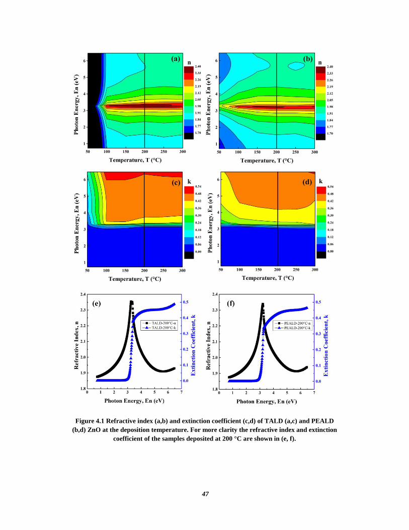
47
Figure 4.1 Refractive index (a,b) and extinction coefficient (c,d) of TALD (a,c) and PEALD
(b,d) ZnO at the deposition temperature. For more clarity the refractive index and extinction
coefficient of the samples deposited at 200 °C are shown in (e, f).
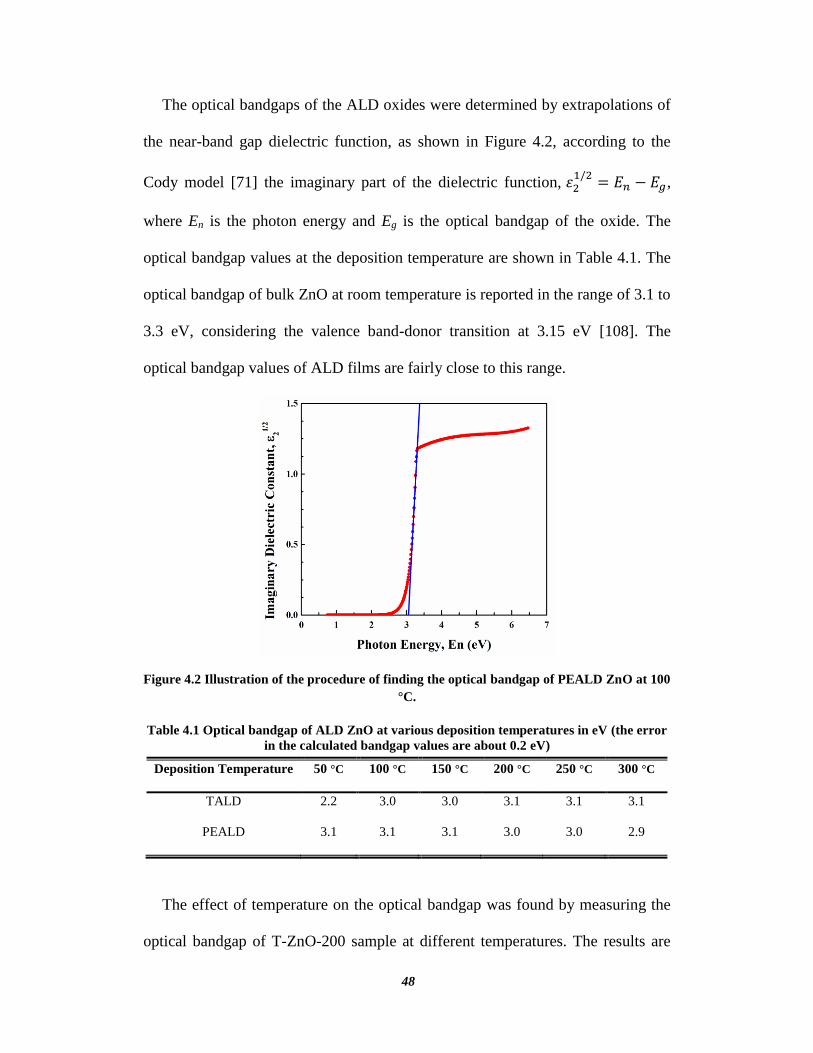
48
The optical bandgaps of the ALD oxides were determined by extrapolations of
the near-band gap dielectric function, as shown in Figure 4.2, according to the
Cody model [71] the imaginary part of the dielectric function,
,
where En is the photon energy and Eg is the optical bandgap of the oxide. The
optical bandgap values at the deposition temperature are shown in Table 4.1. The
optical bandgap of bulk ZnO at room temperature is reported in the range of 3.1 to
3.3 eV, considering the valence band-donor transition at 3.15 eV [108]. The
optical bandgap values of ALD films are fairly close to this range.
Figure 4.2 Illustration of the procedure of finding the optical bandgap of PEALD ZnO at 100
°C.
Table 4.1 Optical bandgap of ALD ZnO at various deposition temperatures in eV (the error
in the calculated bandgap values are about 0.2 eV)
Deposition Temperature 50 °C 100 °C 150 °C 200 °C 250 °C 300 °C
TALD
PEALD
2.2
3.1
3.0
3.1
3.0
3.1
3.1
3.0
3.1
3.0
3.1
2.9
The effect of temperature on the optical bandgap was found by measuring the
optical bandgap of T-ZnO-200 sample at different temperatures. The results are
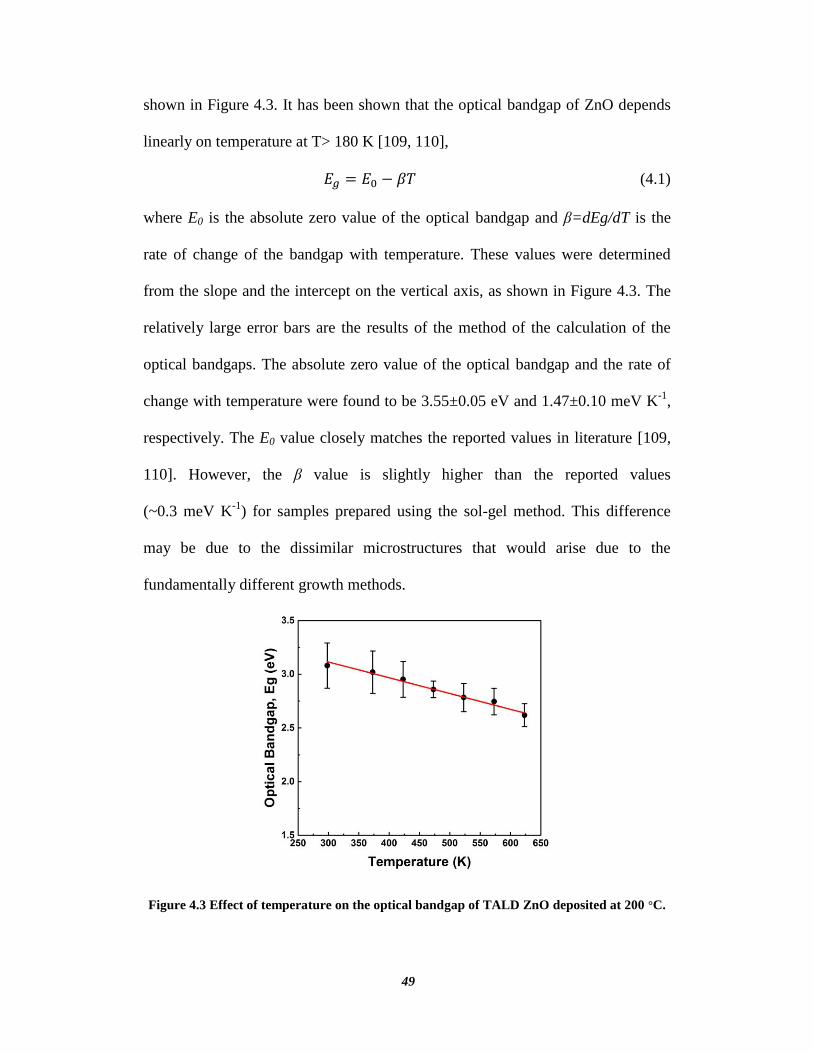
49
shown in Figure 4.3. It has been shown that the optical bandgap of ZnO depends
linearly on temperature at T> 180 K [109, 110],
(4.1)
where E0 is the absolute zero value of the optical bandgap and β=dEg/dT is the
rate of change of the bandgap with temperature. These values were determined
from the slope and the intercept on the vertical axis, as shown in Figure 4.3. The
relatively large error bars are the results of the method of the calculation of the
optical bandgaps. The absolute zero value of the optical bandgap and the rate of
change with temperature were found to be 3.55±0.05 eV and 1.47±0.10 meV K-1
,
respectively. The E0 value closely matches the reported values in literature [109,
110]. However, the β value is slightly higher than the reported values
(~0.3 meV K-1
) for samples prepared using the sol-gel method. This difference
may be due to the dissimilar microstructures that would arise due to the
fundamentally different growth methods.
Figure 4.3 Effect of temperature on the optical bandgap of TALD ZnO deposited at 200 °C.
50
Two explanations have been given for the shift of the direct bandgap with
temperature in the semiconductors [111]: (1) lattice thermal expansion which is
related to the change of electron energies with the volume, and (2) direct
renormalization of the band energies due to the temperature dependence of the
electron–phonon interactions.
4.3.2 Saturation curves and GPC
The ALD saturation curves for TALD and PEALD of ZnO are shown in Figure
4.4. The minimum dose time for saturation of GPC is 20ms for DEZ, 0.1s for H2O
and 2.0s for oxygen plasma.
The dependence of growth per cycle (GPC) of the ALD oxides on deposition
temperature is shown in Figure 4.5. For both ALD techniques the GPC increased
with deposition temperature and reached a maximum at 150 °C. The ALD
window is in the range of 100-200 °C and is in agreement with the existing
literature [89, 97]. More insightful explanation of the behavior of the GPC with
deposition temperature is discussed later in section 4.4, where the reaction
pathways of surface chemical reactions are discussed using density functional
theory (DFT) calculations.
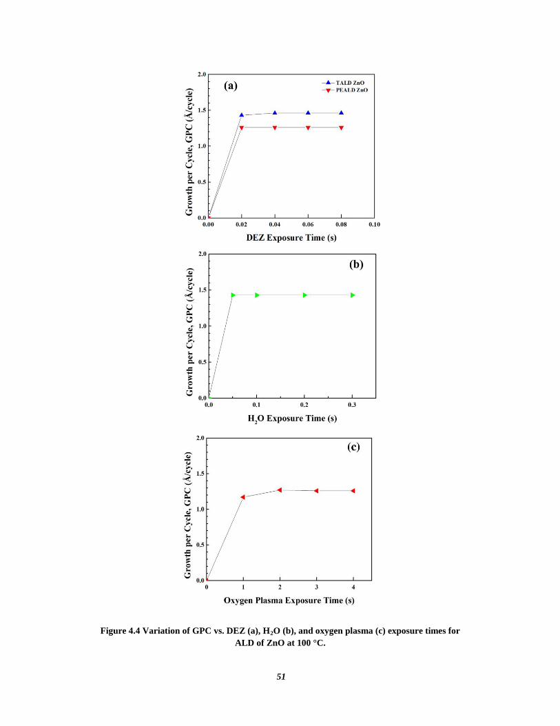
51
Figure 4.4 Variation of GPC vs. DEZ (a), H2O (b), and oxygen plasma (c) exposure times for
ALD of ZnO at 100 °C.
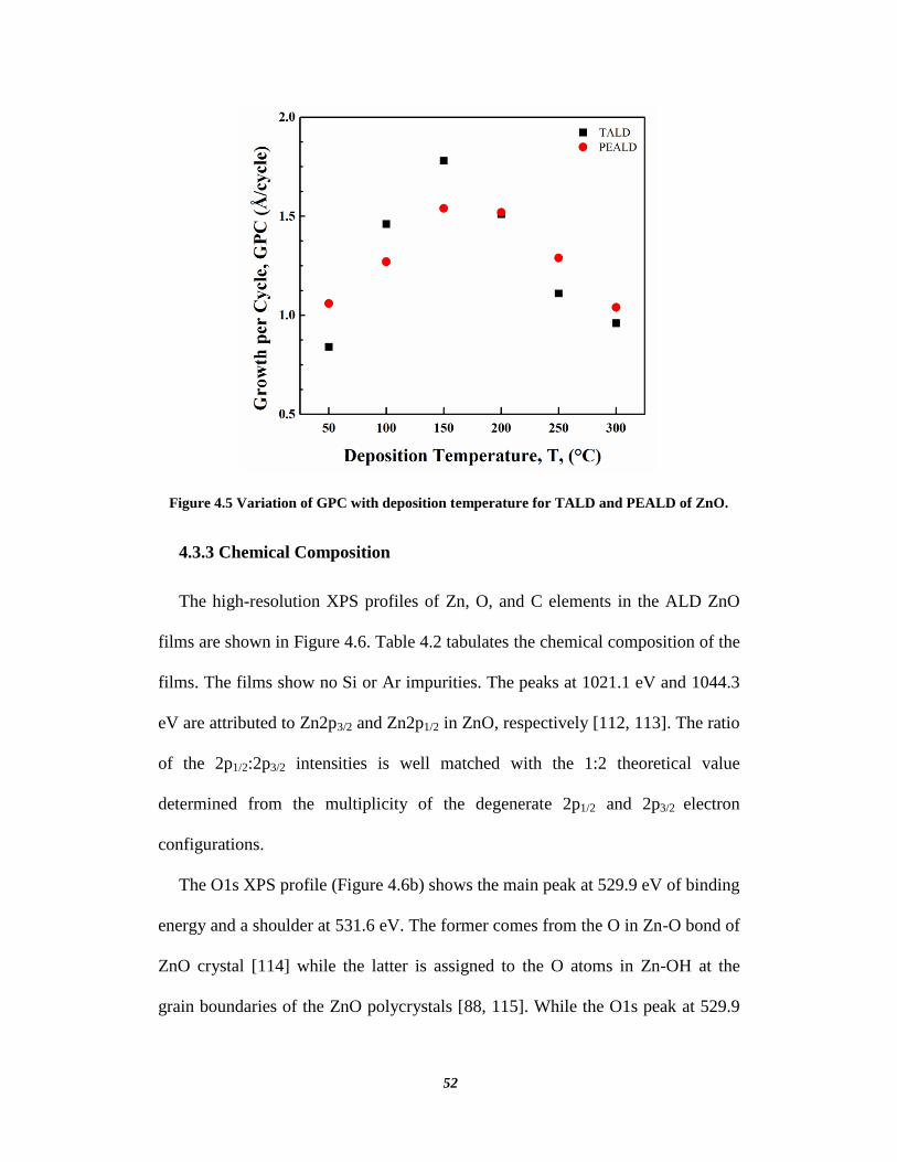
52
Figure 4.5 Variation of GPC with deposition temperature for TALD and PEALD of ZnO.
4.3.3 Chemical Composition
The high-resolution XPS profiles of Zn, O, and C elements in the ALD ZnO
films are shown in Figure 4.6. Table 4.2 tabulates the chemical composition of the
films. The films show no Si or Ar impurities. The peaks at 1021.1 eV and 1044.3
eV are attributed to Zn2p3/2 and Zn2p1/2 in ZnO, respectively [112, 113]. The ratio
of the 2p1/2:2p3/2 intensities is well matched with the 1:2 theoretical value
determined from the multiplicity of the degenerate 2p1/2 and 2p3/2 electron
configurations.
The O1s XPS profile (Figure 4.6b) shows the main peak at 529.9 eV of binding
energy and a shoulder at 531.6 eV. The former comes from the O in Zn-O bond of
ZnO crystal [114] while the latter is assigned to the O atoms in Zn-OH at the
grain boundaries of the ZnO polycrystals [88, 115]. While the O1s peak at 529.9
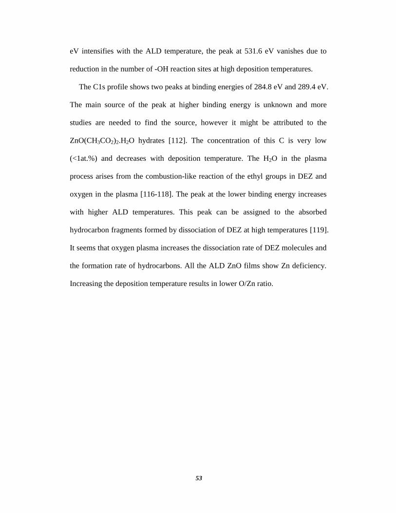
53
eV intensifies with the ALD temperature, the peak at 531.6 eV vanishes due to
reduction in the number of -OH reaction sites at high deposition temperatures.
The C1s profile shows two peaks at binding energies of 284.8 eV and 289.4 eV.
The main source of the peak at higher binding energy is unknown and more
studies are needed to find the source, however it might be attributed to the
ZnO(CH3CO2)2.H2O hydrates [112]. The concentration of this C is very low
(<1at.%) and decreases with deposition temperature. The H2O in the plasma
process arises from the combustion-like reaction of the ethyl groups in DEZ and
oxygen in the plasma [116-118]. The peak at the lower binding energy increases
with higher ALD temperatures. This peak can be assigned to the absorbed
hydrocarbon fragments formed by dissociation of DEZ at high temperatures [119].
It seems that oxygen plasma increases the dissociation rate of DEZ molecules and
the formation rate of hydrocarbons. All the ALD ZnO films show Zn deficiency.
Increasing the deposition temperature results in lower O/Zn ratio.
54
Figure 4.6 High Resolution XPS graphs of Zn2p (a), O1s (b), and C1s (c), for ALD ZnO with
different deposition conditions.
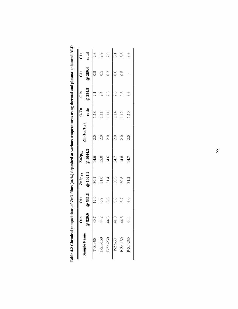
55
Ta
ble
4.2
Ch
em
ica
l co
mp
osi
tio
ns
of
Zn
O f
ilm
s (a
t.%
) d
epo
site
d a
t v
ari
ou
s te
mp
era
ture
s u
sin
g t
her
ma
l a
nd
pla
sma
-en
ha
nce
d A
LD
Sa
mp
le N
am
e
O1
s
@ 5
29
.9
O1
s
@ 5
31
.6
Zn
2p
3/2
@ 1
02
1.2
Zn
2p
1/2
@ 1
04
4.3
Z
n (
I 3/2
/I1/2
) O
/Zn
rati
o
C1
s
@ 2
84
.8
C1
s
@ 2
89
.4
C1
s
tota
l
T-Z
n-5
0
T-Z
n-1
50
T-Z
n-2
50
40
.7
44
.2
44
.5
12
.0
6.9
6.6
30
.1
31
.0
31
.4
14
.6
15
.0
14
.6
2.0
2.0
2.0
1.1
8
1.1
1
1.1
1
2.1
2.4
2.6
0.5
0.5
0.3
2.6
2.9
2.9
P-Z
n-5
0
P-Z
n-1
50
P-Z
n-2
50
41
.9
44
.3
44
.4
9.8
6.7
6.0
30
.5
30
.8
31
.2
14
.7
14
.8
14
.7
2.0
2.0
2.0
1.1
4
1.1
2
1.1
0
2.5
2.8
3.6
0.6
0.5
-
3.1
3.3
3.6
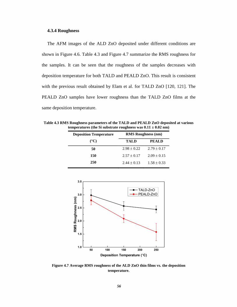
56
4.3.4 Roughness
The AFM images of the ALD ZnO deposited under different conditions are
shown in Figure 4.6. Table 4.3 and Figure 4.7 summarize the RMS roughness for
the samples. It can be seen that the roughness of the samples decreases with
deposition temperature for both TALD and PEALD ZnO. This result is consistent
with the previous result obtained by Elam et al. for TALD ZnO [120, 121]. The
PEALD ZnO samples have lower roughness than the TALD ZnO films at the
same deposition temperature.
Table 4.3 RMS Roughness parameters of the TALD and PEALD ZnO deposited at various
temperatures (the Si substrate roughness was 0.11 ± 0.02 nm)
Deposition Temperature
(°C)
RMS Roughness (nm)
TALD PEALD
50
150
250
2.98 0.22
2.57 0.17
2.44 0.13
2.79 0.17
2.09 0.15
1.58 0.33
Figure 4.7 Average RMS roughness of the ALD ZnO thin films vs. the deposition
temperature.
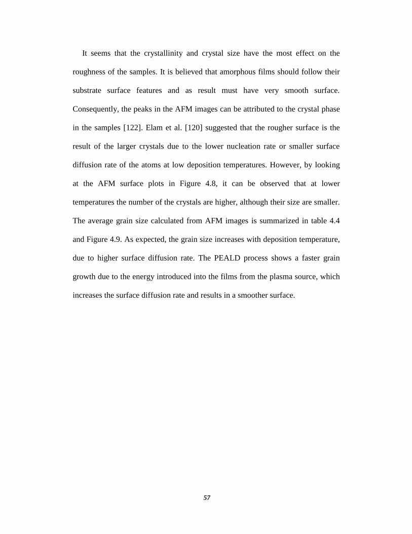
57
It seems that the crystallinity and crystal size have the most effect on the
roughness of the samples. It is believed that amorphous films should follow their
substrate surface features and as result must have very smooth surface.
Consequently, the peaks in the AFM images can be attributed to the crystal phase
in the samples [122]. Elam et al. [120] suggested that the rougher surface is the
result of the larger crystals due to the lower nucleation rate or smaller surface
diffusion rate of the atoms at low deposition temperatures. However, by looking
at the AFM surface plots in Figure 4.8, it can be observed that at lower
temperatures the number of the crystals are higher, although their size are smaller.
The average grain size calculated from AFM images is summarized in table 4.4
and Figure 4.9. As expected, the grain size increases with deposition temperature,
due to higher surface diffusion rate. The PEALD process shows a faster grain
growth due to the energy introduced into the films from the plasma source, which
increases the surface diffusion rate and results in a smoother surface.
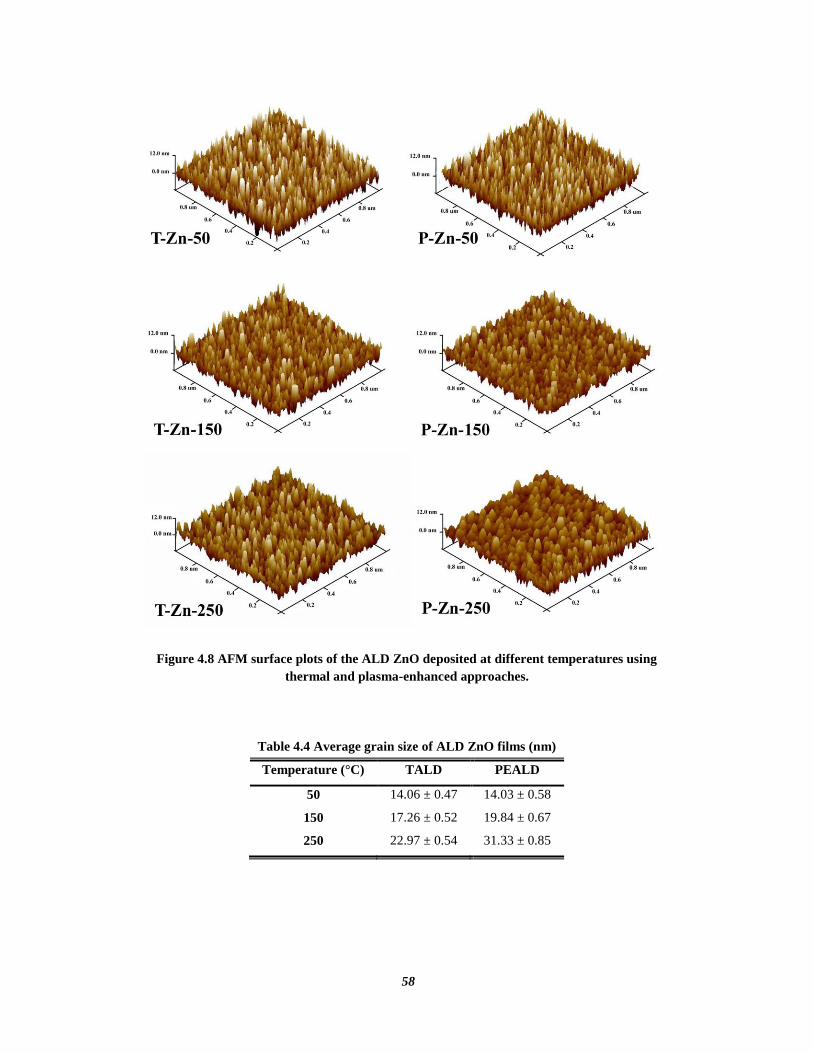
58
Figure 4.8 AFM surface plots of the ALD ZnO deposited at different temperatures using
thermal and plasma-enhanced approaches.
Table 4.4 Average grain size of ALD ZnO films (nm)
Temperature (°C) TALD PEALD
50
150
250
14.06 ± 0.47
17.26 ± 0.52
22.97 ± 0.54
14.03 ± 0.58
19.84 ± 0.67
31.33 ± 0.85
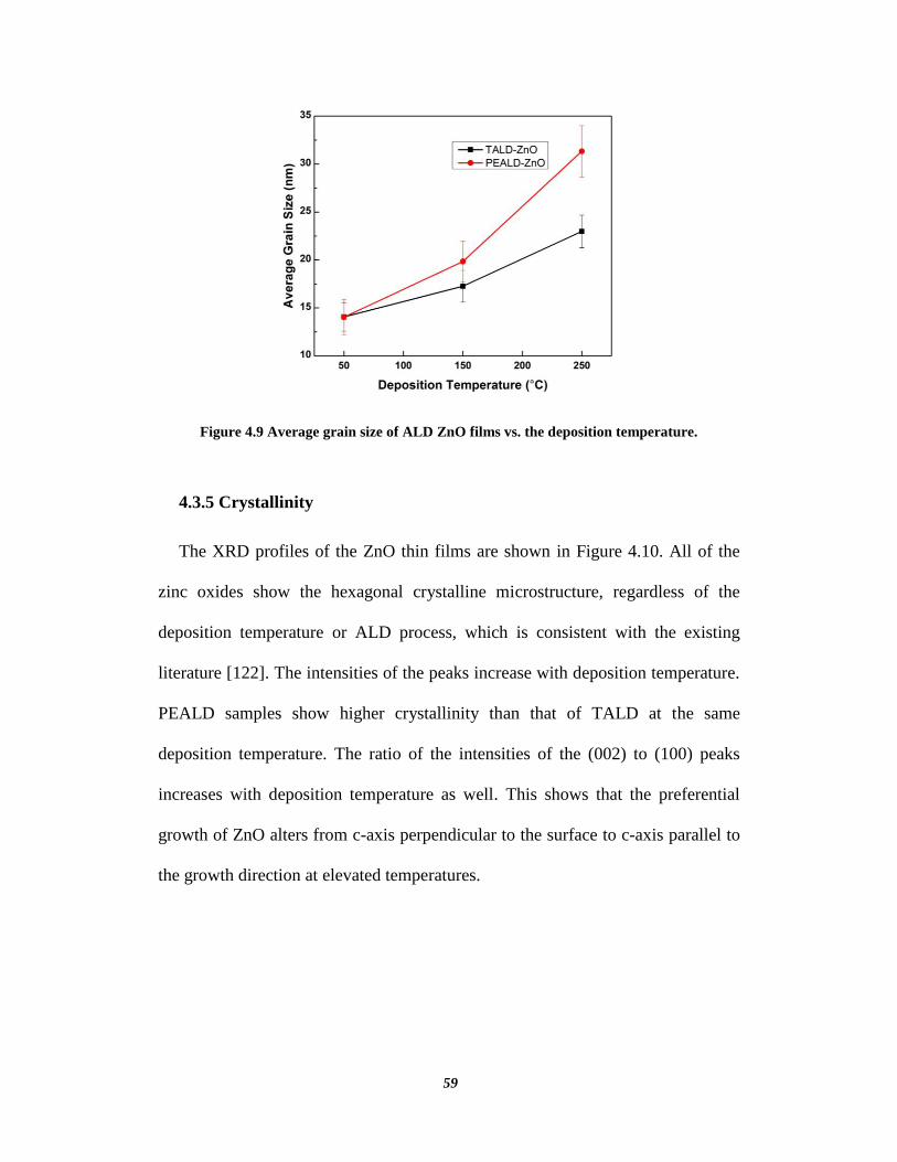
59
Figure 4.9 Average grain size of ALD ZnO films vs. the deposition temperature.
4.3.5 Crystallinity
The XRD profiles of the ZnO thin films are shown in Figure 4.10. All of the
zinc oxides show the hexagonal crystalline microstructure, regardless of the
deposition temperature or ALD process, which is consistent with the existing
literature [122]. The intensities of the peaks increase with deposition temperature.
PEALD samples show higher crystallinity than that of TALD at the same
deposition temperature. The ratio of the intensities of the (002) to (100) peaks
increases with deposition temperature as well. This shows that the preferential
growth of ZnO alters from c-axis perpendicular to the surface to c-axis parallel to
the growth direction at elevated temperatures.
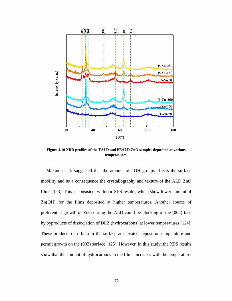
60
Figure 4.10 XRD profiles of the TALD and PEALD ZnO samples deposited at various
temperatures.
Makino et al. suggested that the amount of –OH groups affects the surface
mobility and as a consequence the crystallography and texture of the ALD ZnO
films [123]. This is consistent with our XPS results, which show lower amount of
Zn(OH) for the films deposited at higher temperatures. Another source of
preferential growth of ZnO during the ALD could be blocking of the (002) face
by byproducts of dissociation of DEZ (hydrocarbons) at lower temperatures [124].
These products desorb from the surface at elevated deposition temperature and
permit growth on the (002) surface [125]. However, in this study, the XPS results
show that the amount of hydrocarbons in the films increases with the temperature.
61
It seems that –OH groups has more influence on the preferential growth of the
ZnO than physisorbed hydrocarbon species.
It must be mentioned that chemistry of the substrate and its crystallographic
orientation, the chemistry of the precursors, ALD film thickness, and dose and
purge time durations can affect the crystallinity and roughness of the ZnO films
[125]. All of these parameters were kept constant during this thesis.
Based on the above observations, a model for crystal growth of the ALD ZnO
samples is proposed. The ZnO grains nucleate at random crystallographic
directions at low deposition temperatures. The surface migration is limited by the
high concentration of –OH groups and low deposition temperature. As a result a
columnar growth of ZnO crystals is observed, which leads to a rough ZnO surface.
By increasing the deposition temperature, the –OH group concentration decreases
and the surface diffusion of atoms become more convenient, and the grains start
to grow laterally. The [0001] direction is the preferential orientation because of
the surface energy considerations [126]. Based on this model, elongating the
purge time shifts the preferred orientation towards [0001] direction due to extra
time available for the adsorbed species to desorb from the surface and –OH
groups to recombine and desorb from the surface in form of H2O. This model
agrees well with the experimental results from Malm et al. [127], who showed
high (002) peak intensities at low temperature by using relatively long purge
times. Using oxygen plasma, or molecular oxygen, also changes the crystals
orientation towards [0001] due to lower –OH concentration on the surface and at
the grain boundaries. This matches with Park and Lee’s [128] observations and
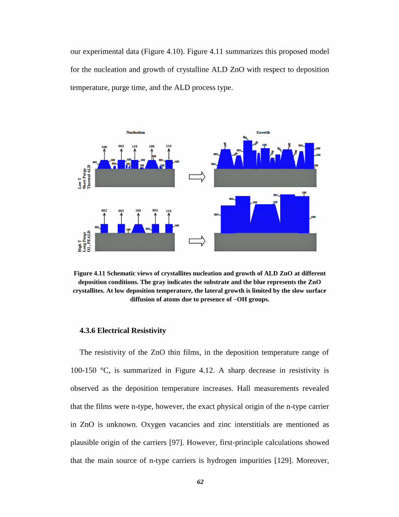
62
our experimental data (Figure 4.10). Figure 4.11 summarizes this proposed model
for the nucleation and growth of crystalline ALD ZnO with respect to deposition
temperature, purge time, and the ALD process type.
Figure 4.11 Schematic views of crystallites nucleation and growth of ALD ZnO at different
deposition conditions. The gray indicates the substrate and the blue represents the ZnO
crystallites. At low deposition temperature, the lateral growth is limited by the slow surface
diffusion of atoms due to presence of –OH groups.
4.3.6 Electrical Resistivity
The resistivity of the ZnO thin films, in the deposition temperature range of
100-150 °C, is summarized in Figure 4.12. A sharp decrease in resistivity is
observed as the deposition temperature increases. Hall measurements revealed
that the films were n-type, however, the exact physical origin of the n-type carrier
in ZnO is unknown. Oxygen vacancies and zinc interstitials are mentioned as
plausible origin of the carriers [97]. However, first-principle calculations showed
that the main source of n-type carriers is hydrogen impurities [129]. Moreover,

63
the zinc vacancies, , act as the compensating sites for n-carriers in n-ZnO
[130]. This explanation agrees with our XPS results, which showed that the Zn
deficiency of the samples decreases with increasing deposition temperature. On
the other hand, although the hydrogen impurities cannot be detected by XPS, our
XPS results showed that the amount of hydrocarbons increased with the
deposition temperature. These results might indicate that the amount of hydrogen
in samples deposited at higher deposition temperatures is larger and as a
consequence they show much lower resistivity.
Figure 4.12 Variation of electrical resistivity of TALD ZnO with the deposition temperature.
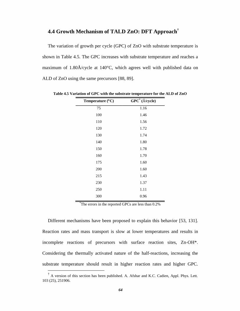
64
4.4 Growth Mechanism of TALD ZnO: DFT Approach†
The variation of growth per cycle (GPC) of ZnO with substrate temperature is
shown in Table 4.5. The GPC increases with substrate temperature and reaches a
maximum of 1.80Å/cycle at 140°C, which agrees well with published data on
ALD of ZnO using the same precursors [88, 89].
Table 4.5 Variation of GPC with the substrate temperature for the ALD of ZnO
Temperature (C) GPC* ( /cycle)
75
100
110
120
130
140
150
160
175
200
215
230
250
300
1.16
1.46
1.56
1.72
1.74
1.80
1.78
1.70
1.60
1.60
1.43
1.37
1.11
0.96
*The errors in the reported GPCs are less than 0.2%
Different mechanisms have been proposed to explain this behavior [53, 131].
Reaction rates and mass transport is slow at lower temperatures and results in
incomplete reactions of precursors with surface reaction sites, Zn-OH*.
Considering the thermally activated nature of the half-reactions, increasing the
substrate temperature should result in higher reaction rates and higher GPC.
† A version of this section has been published. A. Afshar and K.C. Cadien, Appl. Phys. Lett.
103 (25), 251906.
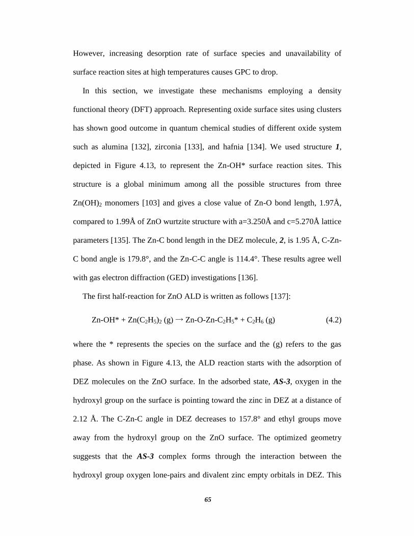
65
However, increasing desorption rate of surface species and unavailability of
surface reaction sites at high temperatures causes GPC to drop.
In this section, we investigate these mechanisms employing a density
functional theory (DFT) approach. Representing oxide surface sites using clusters
has shown good outcome in quantum chemical studies of different oxide system
such as alumina [132], zirconia [133], and hafnia [134]. We used structure 1,
depicted in Figure 4.13, to represent the Zn-OH* surface reaction sites. This
structure is a global minimum among all the possible structures from three
Zn(OH)2 monomers [103] and gives a close value of Zn-O bond length, 1.97Å,
compared to 1.99Å of ZnO wurtzite structure with a=3.250Å and c=5.270Å lattice
parameters [135]. The Zn-C bond length in the DEZ molecule, 2, is 1.95 Å, C-Zn-
C bond angle is 179.8°, and the Zn-C-C angle is 114.4°. These results agree well
with gas electron diffraction (GED) investigations [136].
The first half-reaction for ZnO ALD is written as follows [137]:
Zn-OH* + Zn(C2H5)2 (g) → Zn-O-Zn-C2H5* + C2H6 (g) (4.2)
where the * represents the species on the surface and the (g) refers to the gas
phase. As shown in Figure 4.13, the ALD reaction starts with the adsorption of
DEZ molecules on the ZnO surface. In the adsorbed state, AS-3, oxygen in the
hydroxyl group on the surface is pointing toward the zinc in DEZ at a distance of
2.12 Å. The C-Zn-C angle in DEZ decreases to 157.8° and ethyl groups move
away from the hydroxyl group on the ZnO surface. The optimized geometry
suggests that the AS-3 complex forms through the interaction between the
hydroxyl group oxygen lone-pairs and divalent zinc empty orbitals in DEZ. This
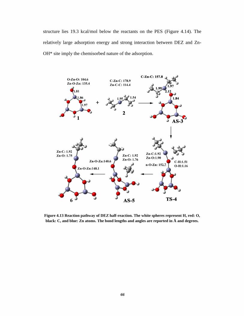
66
structure lies 19.3 kcal/mol below the reactants on the PES (Figure 4.14). The
relatively large adsorption energy and strong interaction between DEZ and Zn-
OH* site imply the chemisorbed nature of the adsorption.
Figure 4.13 Reaction pathway of DEZ half-reaction. The white spheres represent H, red: O,
black: C, and blue: Zn atoms. The bond lengths and angles are reported in Å and degrees.
67
Figure 4.14 Potential energy surface for the DEZ half-reaction. The calculations were
carried out at the B3LYP/6-311G(d) level. The enthalpy values are reported at 0 K. For
clarity, the ZnO structure in the reactions is shown with a smaller cluster.
The ALD reaction proceeds by formation of a four-center transition state, TS-4,
between O-H-Zn-C atoms. The transition vector is dominated by the movement of
the H atom from a hydroxyl group to an ethyl ligand to form ethane. In TS-4, one
of the Zn-C bonds in DEZ is broken and the Zn-C distance increases from 1.95Å
to 2.38Å. The Zn-O bond forms between Zn in DEZ and O in the hydroxyl site on
the ZnO surface and the O-H distance increases from 0.95Å in the chemisorbed
state to 1.16Å in the transition state. Concurrently, the C-H distance decreases to
1.51Å from the 3.14Å in AS-3. TS-4 lies 11.8 kcal/mol above the reactants and
31.1 kcal/mol above the chemisorbed state on the PES, which shows the reaction
must gain supplementary energy to proceed.
In the post transition state structure, AS-5, C2H6 is adsorbed on the ZnO
surface. AS-5 lies 11.9 kcal/mol lower than the desorbed state, 6 + C2H6, on the
PES and the distance of the ethane molecule is 3.43Å from the oxygen in ZnO.
This implies that the interaction of C2H6 with surface is not strong and the
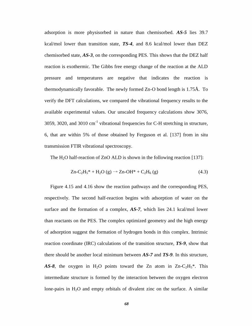
68
adsorption is more physisorbed in nature than chemisorbed. AS-5 lies 39.7
kcal/mol lower than transition state, TS-4, and 8.6 kcal/mol lower than DEZ
chemisorbed state, AS-3, on the corresponding PES. This shows that the DEZ half
reaction is exothermic. The Gibbs free energy change of the reaction at the ALD
pressure and temperatures are negative that indicates the reaction is
thermodynamically favorable. The newly formed Zn-O bond length is 1.75Å. To
verify the DFT calculations, we compared the vibrational frequency results to the
available experimental values. Our unscaled frequency calculations show 3076,
3059, 3020, and 3010 cm-1
vibrational frequencies for C-H stretching in structure,
6, that are within 5% of those obtained by Ferguson et al. [137] from in situ
transmission FTIR vibrational spectroscopy.
The H2O half-reaction of ZnO ALD is shown in the following reaction [137]:
Zn-C2H5* + H2O (g) → Zn-OH* + C2H6 (g) (4.3)
Figure 4.15 and 4.16 show the reaction pathways and the corresponding PES,
respectively. The second half-reaction begins with adsorption of water on the
surface and the formation of a complex, AS-7, which lies 24.1 kcal/mol lower
than reactants on the PES. The complex optimized geometry and the high energy
of adsorption suggest the formation of hydrogen bonds in this complex. Intrinsic
reaction coordinate (IRC) calculations of the transition structure, TS-9, show that
there should be another local minimum between AS-7 and TS-9. In this structure,
AS-8, the oxygen in H2O points toward the Zn atom in Zn-C2H5*. This
intermediate structure is formed by the interaction between the oxygen electron
lone-pairs in H2O and empty orbitals of divalent zinc on the surface. A similar
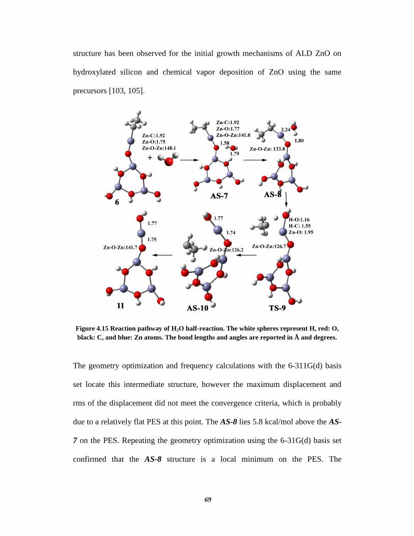
69
structure has been observed for the initial growth mechanisms of ALD ZnO on
hydroxylated silicon and chemical vapor deposition of ZnO using the same
precursors [103, 105].
Figure 4.15 Reaction pathway of H2O half-reaction. The white spheres represent H, red: O,
black: C, and blue: Zn atoms. The bond lengths and angles are reported in Å and degrees.
The geometry optimization and frequency calculations with the 6-311G(d) basis
set locate this intermediate structure, however the maximum displacement and
rms of the displacement did not meet the convergence criteria, which is probably
due to a relatively flat PES at this point. The AS-8 lies 5.8 kcal/mol above the AS-
7 on the PES. Repeating the geometry optimization using the 6-31G(d) basis set
confirmed that the AS-8 structure is a local minimum on the PES. The
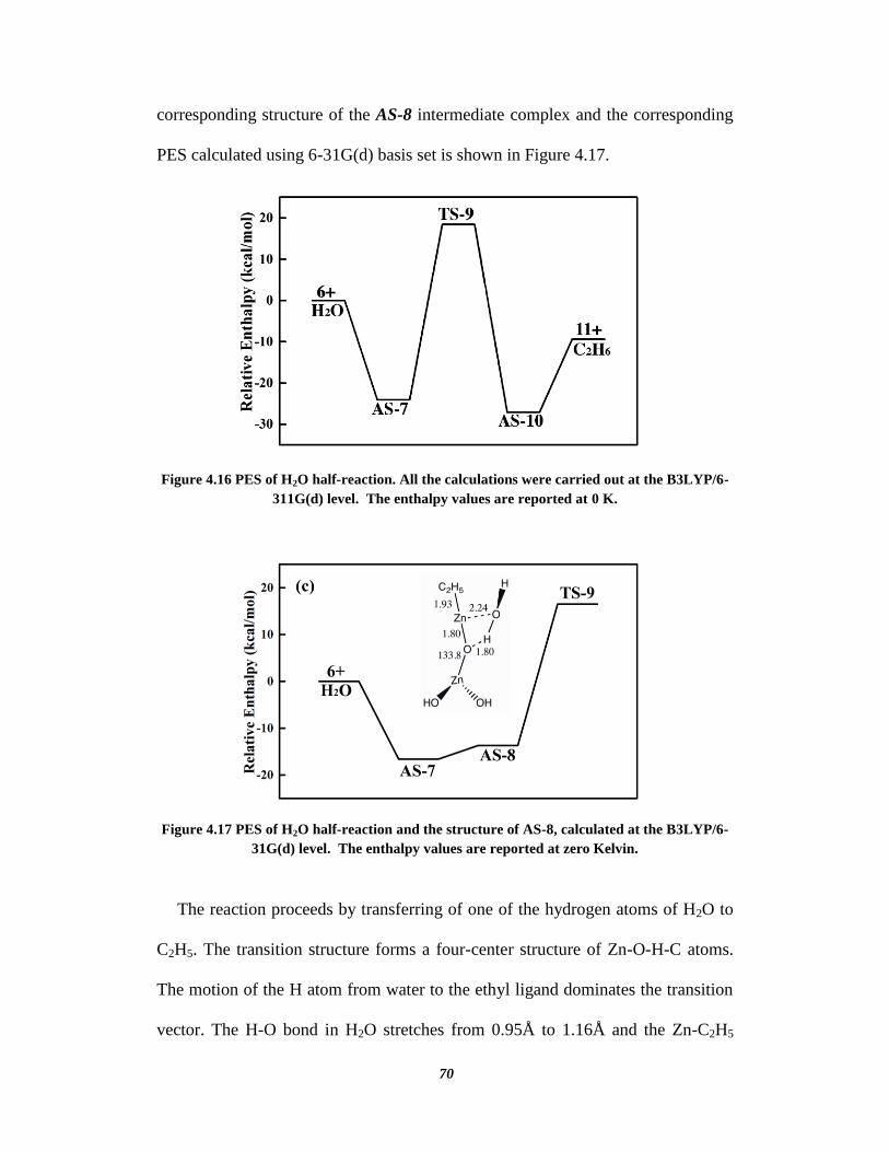
70
corresponding structure of the AS-8 intermediate complex and the corresponding
PES calculated using 6-31G(d) basis set is shown in Figure 4.17.
Figure 4.16 PES of H2O half-reaction. All the calculations were carried out at the B3LYP/6-
311G(d) level. The enthalpy values are reported at 0 K.
Figure 4.17 PES of H2O half-reaction and the structure of AS-8, calculated at the B3LYP/6-
31G(d) level. The enthalpy values are reported at zero Kelvin.
The reaction proceeds by transferring of one of the hydrogen atoms of H2O to
C2H5. The transition structure forms a four-center structure of Zn-O-H-C atoms.
The motion of the H atom from water to the ethyl ligand dominates the transition
vector. The H-O bond in H2O stretches from 0.95Å to 1.16Å and the Zn-C2H5
71
bond breaks completely. The Zn-C distance increases to 2.24Å in the transition
structure. The H-C2H5 bond forms and its length is 1.55Å in TS-9. The transition
structure, TS-9, lies 18.4 kcal/mol above the reactants on the PES. This means
that the second half-reaction requires an additional energy to proceed.
The post-transition complex, AS-10 lies 45.2 kcal/mol below the TS-9 on the
PES. The C2H6 locates 3.68Å above the ZnO surface, with one of its C-H bonds
pointing towards oxygen in ZnO. The desorbed state of C2H6 from the ZnO
surface, 11, is located 16.7 kcal/mol higher on the PES than the post-reaction
complex, AS-10. The products of the second ALD half-reaction lie 9.4 kcal/mol
lower than the reactants on the corresponding PES, which indicates that the
second half-reaction is exothermic. The Gibbs free energy of the reaction is
negative at all the ALD temperatures, which means the reaction is
thermodynamically favorable. The unscaled 3848 cm-1
stretching mode for the
OH bond on ZnO surface is within 5% of in situ FTIR studies by Ferguson et al.
[137].
We also used a smaller, Zn(OH2), and a larger cluster, (Zn9O9H6-(OH)6),
composed of three layers of structure 1, to study the effect of near neighbor atoms
on the surface reactions (Figure 4.18). These clusters were used to calculate the
overall half-reaction thermodynamics and the geometry of the reactants and by-
products (Table 4.6). The comparison between the half-reaction enthalpies, Gibbs
free energies, and the geometries of the surface by-products for different clusters
showed that the reactions are fairly insensitive to the cluster size and structure 1 is
a good model for the reaction site.
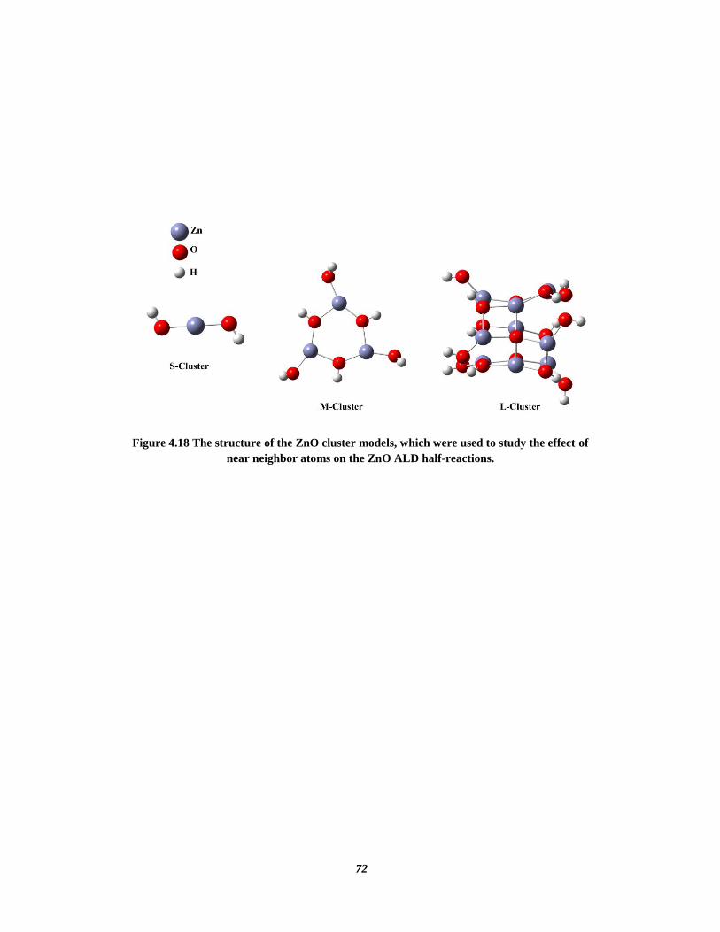
72
Figure 4.18 The structure of the ZnO cluster models, which were used to study the effect of
near neighbor atoms on the ZnO ALD half-reactions.
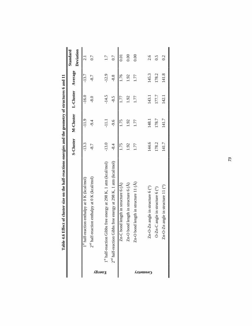
73
Ta
ble
4.6
Eff
ect
of
clu
ster
siz
e o
n t
he
ha
lf-r
ea
ctio
ns
ener
gie
s a
nd
th
e g
eom
etry
of
stru
ctu
res
6 a
nd
11
S
-Clu
ster
M
-Clu
ster
L
-Clu
ster
A
ver
ag
e S
tan
da
rd
Dev
iati
on
Energy
1st h
alf-
reac
tio
n e
nth
alp
y a
t 0
K (
kca
l/m
ol)
2n
d h
alf-
reac
tio
n e
nth
alp
y a
t 0
K (
kca
l/m
ol)
1st h
alf-
reac
tio
n G
ibb
s fr
ee e
ner
gy a
t 2
98
K,
1 a
tm (
kca
l/m
ol)
2n
d h
alf-
reac
tio
n G
ibb
s fr
ee e
ner
gy a
t 2
98
K,
1 a
tm (
kca
l/m
ol)
-13
.3
-8.7
-13
.0
-8.4
-11
.9
-9.4
-11
.1
-9.6
-16
.0
-8.0
-14
.5
-8.5
-13
.7
-8.7
-12
.9
-8.8
2.1
0.7
1.7
0.7
Geometry
Zn-C
bo
nd
len
gth
in s
truct
ure
6 (
Å)
Zn-O
bo
nd
len
gth
in s
truct
ure
6 (
Å)
Zn-O
bo
nd
len
gth
in s
truct
ure
11
(Å
)
Zn-O
-Zn a
ngle
in s
truct
ure
6 (
°)
O-Z
n-C
an
gle
in s
truct
ure
6 (
°)
Zn-O
-Zn a
ngle
in s
truct
ure
11
(°)
1.7
5
1.9
2
1.7
7
14
4.6
17
8.2
14
1.7
1.7
5
1.9
2
1.7
7
14
8.1
17
8.7
14
1.7
1.7
7
1.9
2
1.7
7
14
3.1
17
7.7
14
2.1
1.7
6
1.9
2
1.7
7
14
5.3
17
8.2
14
1.8
0.0
1
0.0
0
0.0
0
2.6
0.5
0.2
74
It can be deduced from the previous discussion that both ALD half-reactions
involve formation of intermediate complexes. These complexes form between
DEZ and Zn-OH* in the 1st half-reaction, AS-3, and between H2O and Zn-C2H5*
in 2nd
half-reaction, AS-8. The variations of the Gibbs free energy of formation of
these complexes with temperature are shown in Figure 4.19 along with GPC of
ALD ZnO. At temperatures higher than 120°C the desorbed state of DEZ is more
stable than its chemisorbed state. This occurs for the H2O half-reaction at
temperatures above 200°C. In other words, the formation of the complexes
becomes more thermodynamically unfavorable with increasing ALD temperature.
At high temperatures, the entropy-temperature product becomes much larger than
the enthalpy and dominates Gibbs free energy. In chemisorbed states, the motions
of adsorbates are limited compared to motions in the gaseous state. Consequently,
the desorbed states of precursors have higher entropy and become more stable
than the adsorbed states with increasing temperature. The stability of the
complexes directly influences the growth rate of ALD ZnO. This is shown in
Figure 4.19, where the rate of variation of GPC with temperature starts to change
at about the same temperatures that the Gibbs free energies of adsorption of the
precursors change sign to positive.
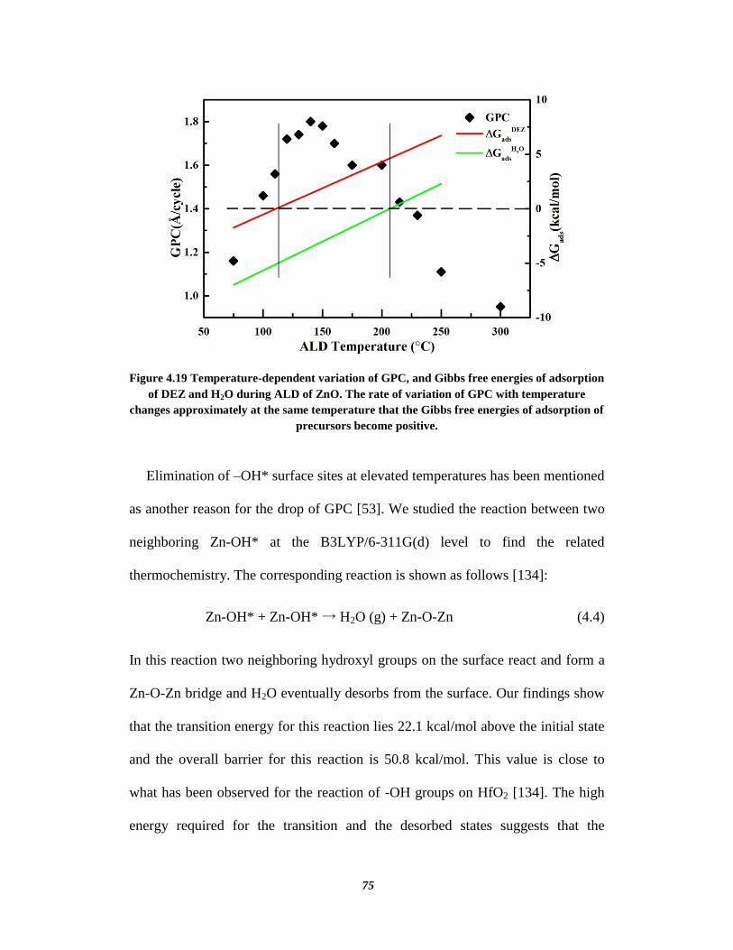
75
Figure 4.19 Temperature-dependent variation of GPC, and Gibbs free energies of adsorption
of DEZ and H2O during ALD of ZnO. The rate of variation of GPC with temperature
changes approximately at the same temperature that the Gibbs free energies of adsorption of
precursors become positive.
Elimination of –OH* surface sites at elevated temperatures has been mentioned
as another reason for the drop of GPC [53]. We studied the reaction between two
neighboring Zn-OH* at the B3LYP/6-311G(d) level to find the related
thermochemistry. The corresponding reaction is shown as follows [134]:
Zn-OH* + Zn-OH* → H2O (g) + Zn-O-Zn (4.4)
In this reaction two neighboring hydroxyl groups on the surface react and form a
Zn-O-Zn bridge and H2O eventually desorbs from the surface. Our findings show
that the transition energy for this reaction lies 22.1 kcal/mol above the initial state
and the overall barrier for this reaction is 50.8 kcal/mol. This value is close to
what has been observed for the reaction of -OH groups on HfO2 [134]. The high
energy required for the transition and the desorbed states suggests that the
76
elimination of the surface reaction sites is less probable in the temperature range
of this study.
4.5 Conclusions
The growth mechanisms of thermal and plasma-enhanced ALD of ZnO were
studied. The saturation curves showed that the optimum values for the exposure
time of DEZ, H2O, and O2-plasma are 0.02, 0.10, and 2.00s, respectively. The
maximum GPC was obtained at 140 °C with a value of 1.80 Å/cycle. The optical
constants of the ALD films were calculated by fitting the spectroscopy
ellipsometric data to a Cody-Lorentz model and showed to meet the bulk values at
deposition temperatures over 100 °C. The optical bandgaps for the samples were
approximately 3.0 eV at all the deposition temperatures above 100 °C. The AFM
studies showed that the roughness of the ZnO thin films decrease with the
deposition temperature. This was attributed to the formation of (002) preferential
orientation in ZnO crystallites at high deposition temperatures due to the much
less –OH concentration on the surface and the grain boundaries. A model for the
growth of ALD ZnO films was proposed based on the experimental results. The
chemical composition of the samples from XPS experiment showed that the ZnO
thin films had a zinc deficiency. The amount of C in the films was less than 4 at.%
for all the deposition temperatures. The main source of the carbon seemed to be
the decomposition of DEZ, especially at high deposition temperatures. A DFT
approach to the growth mechanism of TALD ZnO revealed that the stability of the
intermediate complexes, formed from adsorption of the precursors on the surface,
plays an important role in the growth rate of the ZnO.
77
Chapter 5
Atomic Layer Deposition of Zirconium Oxide
5.1 Introduction
Zirconium oxide (ZrO2), also known as zirconia, has been investigated as a
possible high- oxide candidate for the gate oxide in integrated circuits. It has a
permittivity value of 23 in the monoclinic phase, which can be manipulated by
adding stabilizing yttria cations (3-5 at. % ) to as high as 42 [138]. ZrO2 has a
bandgap of 5.8 eV, which makes it a promising gate oxide for wide bandgap
semiconductor devices [27, 139]. However, HfO2 is currently used for Si devices
due to the reactivity of Zr with Si [140]. ZrO2-Al2O3-ZrO2 (ZAZ) dielectric stack
is currently used in 60nm DRAMs [141, 142]. Moreover, ZrO2 has a good ion
conductivity and can be used in fuel cells as the solid electrolyte [143].
The first ALD of ZrO2 was reported by Ritala and Leskela [144] in 1994, using
ZrCl4 and H2O as the precursors. The film was deposited between 300 and 500 °C,
which was a low temperature range compared to chemical vapor deposition
techniques [144-146]. Using metalorganic precursors, which have higher vapor
pressure, it is possible to deposit ZrO2 at much lower temperatures [147-154].
Among this group of precursors, metal amides are widely used in ALD research
and industry [155]. Metal amides (tetrakis(dimethylamido)zirconium TDMAZr,
for example) have high volatility and are liquid under the vaporization conditions
of ALD, which are benefits in the synthesis, purification, and handling of the
precursor, which makes the ALD process more reproducible and cleaner.
78
Moreover, alkylamides do not harm the substrate surface by producing corrosive
byproducts such as hydrochloric acid, which is one ALD byproduct chloride
precursors are used [155].
Despite several studies on the application of ALD ZrO2 thin films deposited
using metal amides and water or oxygen sources, there is a lack of a systematic
study on the material characterization of ZrO2 ALD films [156-160]. In this
chapter, the chemical composition, crystallinity, roughness, and optical
characterizations of the ZrO2 ALD films deposited using TDMAZr precursor are
presented and discussed. Thermal and plasma-enhanced ALD of ZrO2 at various
deposition temperatures have been studied. TEM images and C-V characteristics
of Cr/ZrO2/GaN MOSCAPs show the high quality of the semiconductor/high-κ
oxide. The results show that ZrO2 is a promising candidate for GaN MOSFETs.
Finally, a density functional approach to the growth mechanism of ZrO2 is
presented.
5.2 Experimental Procedure
The details of the ALD process and substrate preparation are discussed in
Chapter 3. The saturation curves for TDMAZr, H2O, and O2-plama were plotted
at 200 °C to find the optimum dose times. The optimized exposure times at
200 °C were used for the deposition at all the other temperature. XPS, XRD, AFM
characterization were conducted on the 20nm-thick ALD films. More details on
the apparatus and the experimental conditions can be found in Chapter 3.
For the DFT study, GAUSSIAN 09 [100] was used to perform molecular
orbital calculations. The geometry of stationary points were located using the
79
B3LYP gradient corrected density functional method [59-62] with 6-31+G(d,p)
polarized double split valence basis set for nonmetallic atoms [161-168], i.e. H, C,
N, and O, and Los Alamos ECP plus DZ (LanL2DZ) for Zr [169-171]. This level
of theory has shown reliable results in studying growth mechanisms of ALD ZrO2
using ZrCl4 as the precursor [133, 172, 173]. The frequency calculations were
carried out at the same level of theory to identify the nature of the stationary
points (local minima and transition states) and to calculate the zero-point energy
corrections and the thermal corrections at the ALD temperature and pressure. All
reported energies are corrected by the zero-point energy correction value. In order
to test the validity of the calculations, we compared our results with available
experimental data whenever possible.
5.3 Results
5.3.1 Optical Constants
The dependence of the optical constants of TALD and PEALD of ZrO2 on
deposition temperature and photon energy is shown in Figure 5.1. The refractive
index increases with deposition temperature, as the crystallinity and density of the
oxide improve. The maximum refractive index is obtained between 200-250 °C
for both thermal and plasma-enhanced ALD oxides. These values are higher than
values reported previously for films deposited by magnetron sputtering [174] and
e-beam evaporation [175] and match the bulk values [176]. At higher deposition
temperature (T>250 °C) the refractive index decreases due to decomposition of
the precursor, which results in incorporation of impurities into the thin films [155].
A smoother change in optical profile vs. deposition temperature is observed for
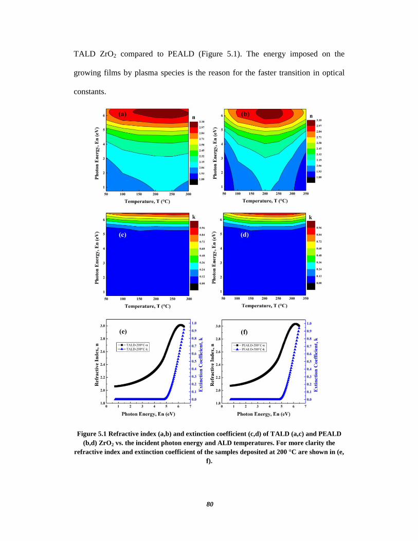
80
TALD ZrO2 compared to PEALD (Figure 5.1). The energy imposed on the
growing films by plasma species is the reason for the faster transition in optical
constants.
Figure 5.1 Refractive index (a,b) and extinction coefficient (c,d) of TALD (a,c) and PEALD
(b,d) ZrO2 vs. the incident photon energy and ALD temperatures. For more clarity the
refractive index and extinction coefficient of the samples deposited at 200 °C are shown in (e,
f).
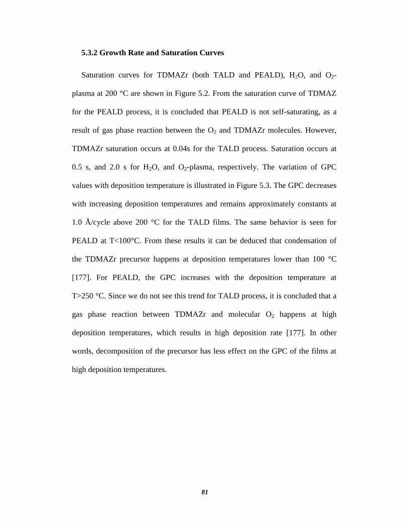
81
5.3.2 Growth Rate and Saturation Curves
Saturation curves for TDMAZr (both TALD and PEALD), H2O, and O2-
plasma at 200 °C are shown in Figure 5.2. From the saturation curve of TDMAZ
for the PEALD process, it is concluded that PEALD is not self-saturating, as a
result of gas phase reaction between the O2 and TDMAZr molecules. However,
TDMAZr saturation occurs at 0.04s for the TALD process. Saturation occurs at
0.5 s, and 2.0 s for H2O, and O2-plasma, respectively. The variation of GPC
values with deposition temperature is illustrated in Figure 5.3. The GPC decreases
with increasing deposition temperatures and remains approximately constants at
1.0 Å/cycle above 200 °C for the TALD films. The same behavior is seen for
PEALD at T<100°C. From these results it can be deduced that condensation of
the TDMAZr precursor happens at deposition temperatures lower than 100 °C
[177]. For PEALD, the GPC increases with the deposition temperature at
T>250 °C. Since we do not see this trend for TALD process, it is concluded that a
gas phase reaction between TDMAZr and molecular O2 happens at high
deposition temperatures, which results in high deposition rate [177]. In other
words, decomposition of the precursor has less effect on the GPC of the films at
high deposition temperatures.
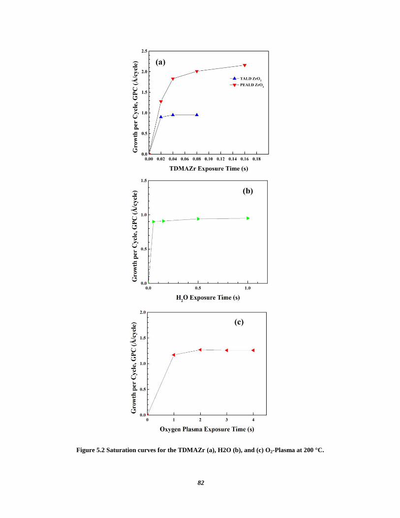
82
Figure 5.2 Saturation curves for the TDMAZr (a), H2O (b), and (c) O2-Plasma at 200 °C.
83
Figure 5.3 GPC of ALD ZrO2 with deposition temperature for both thermal and plasma-
enhanced processes.
5.3.3 Chemical Composition
High-resolution XPS profiles of the ALD ZrO2 thin films are shown in Figure
5.4. The chemical composition of the zirconium oxide is summarized in Table 5.1.
The Zr3d3/2 and Zr3d5/2 peaks are depicted in Figure 5.4a. The binding energy
difference of 2.4eV and the intensity ratio of 1.5 agree with the published values
[178]. The binding energy of Zr3d5/2 has been shown to vary from 180.2 eV to
182.7 eV depending on the oxidation state (Zr2+
: 180.2 eV, Zr3+
: 181.2 eV,
Zr4+
(O2-
): 181.9 eV, and Zr4+
(OH): 182.7 eV) [179-182].
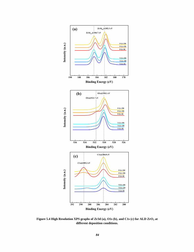
84
Figure 5.4 High Resolution XPS graphs of Zr3d (a), O1s (b), and C1s (c) for ALD ZrO2 at
different deposition conditions.
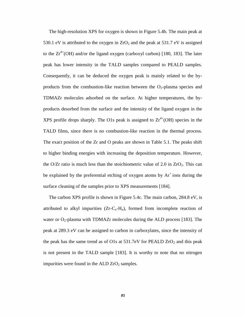
85
The high-resolution XPS for oxygen is shown in Figure 5.4b. The main peak at
530.1 eV is attributed to the oxygen in ZrO2 and the peak at 531.7 eV is assigned
to the Zr4+
(OH) and/or the ligand oxygen (carboxyl carbon) [180, 183]. The later
peak has lower intensity in the TALD samples compared to PEALD samples.
Consequently, it can be deduced the oxygen peak is mainly related to the by-
products from the combustion-like reaction between the O2-plasma species and
TDMAZr molecules adsorbed on the surface. At higher temperatures, the by-
products desorbed from the surface and the intensity of the ligand oxygen in the
XPS profile drops sharply. The O1s peak is assigned to Zr4+
(OH) species in the
TALD films, since there is no combustion-like reaction in the thermal process.
The exact position of the Zr and O peaks are shown in Table 5.1. The peaks shift
to higher binding energies with increasing the deposition temperature. However,
the O/Zr ratio is much less than the stoichiometric value of 2.0 in ZrO2. This can
be explained by the preferential etching of oxygen atoms by Ar+
ions during the
surface cleaning of the samples prior to XPS measurements [184].
The carbon XPS profile is shown in Figure 5.4c. The main carbon, 284.8 eV, is
attributed to alkyl impurities (Zr-Cx-Hn), formed from incomplete reaction of
water or O2-plasma with TDMAZr molecules during the ALD process [183]. The
peak at 289.3 eV can be assigned to carbon in carboxylates, since the intensity of
the peak has the same trend as of O1s at 531.7eV for PEALD ZrO2 and this peak
is not present in the TALD sample [183]. It is worthy to note that no nitrogen
impurities were found in the ALD ZrO2 samples.
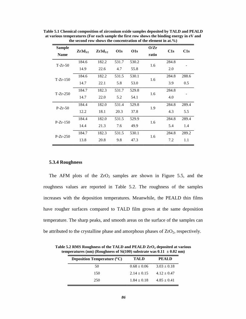
86
Table 5.1 Chemical composition of zirconium oxide samples deposited by TALD and PEALD
at various temperatures (For each sample the first row shows the binding energy in eV and
the second row shows the concentration of the element in at.%)
Sample
Name Zr3d3/2 Zr3d5/2 O1s O1s
O/Zr
ratio C1s C1s
T-Zr-50 184.6 182.2 531.7 530.2
1.6 284.8
- 14.9 22.6 4.7 55.8 2.0
T-Zr-150 184.6 182.2 531.5 530.1
1.6 284.8 288.6
14.7 22.1 5.8 53.0 3.9 0.5
T-Zr-250 184.7 182.3 531.7 529.8
1.6 284.8
- 14.7 22.0 5.2 54.1 4.0
P-Zr-50 184.4 182.0 531.4 529.8
1.9 284.8 289.4
12.2 18.1 20.3 37.8 4.3 5.5
P-Zr-150 184.4 182.0 531.5 529.9
1.6 284.8 289.4
14.4 21.3 7.6 49.9 5.4 1.4
P-Zr-250 184.7 182.3 531.5 530.1
1.6 284.8 289.2
13.8 20.8 9.8 47.3 7.2 1.1
5.3.4 Roughness
The AFM plots of the ZrO2 samples are shown in Figure 5.5, and the
roughness values are reported in Table 5.2. The roughness of the samples
increases with the deposition temperatures. Meanwhile, the PEALD thin films
have rougher surfaces compared to TALD film grown at the same deposition
temperature. The sharp peaks, and smooth areas on the surface of the samples can
be attributed to the crystalline phase and amorphous phases of ZrO2, respectively.
Table 5.2 RMS Roughness of the TALD and PEALD ZrO2 deposited at various
temperatures (nm) (Roughness of Si(100) substrate was 0.11 ± 0.02 nm)
Deposition Temperature (C) TALD PEALD
50
150
250
0.68 ± 0.06
2.14 ± 0.15
1.84 ± 0.18
3.03 ± 0.18
4.12 ± 0.47
4.85 ± 0.41
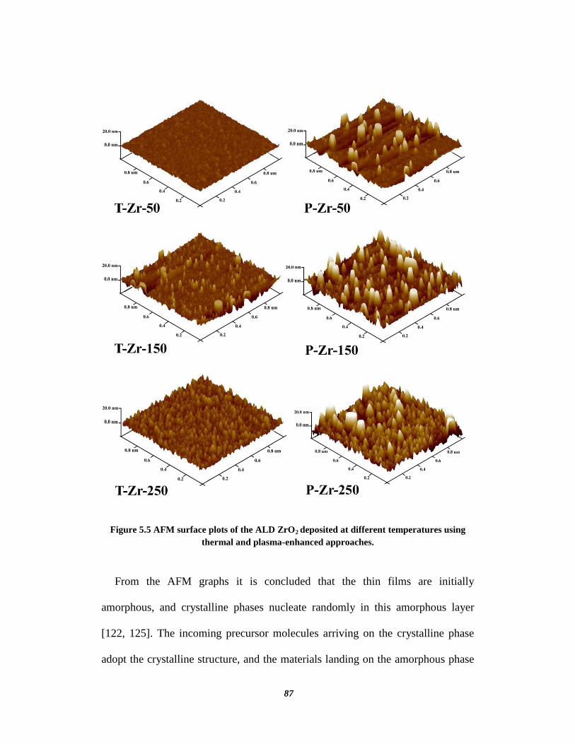
87
Figure 5.5 AFM surface plots of the ALD ZrO2 deposited at different temperatures using
thermal and plasma-enhanced approaches.
From the AFM graphs it is concluded that the thin films are initially
amorphous, and crystalline phases nucleate randomly in this amorphous layer
[122, 125]. The incoming precursor molecules arriving on the crystalline phase
adopt the crystalline structure, and the materials landing on the amorphous phase
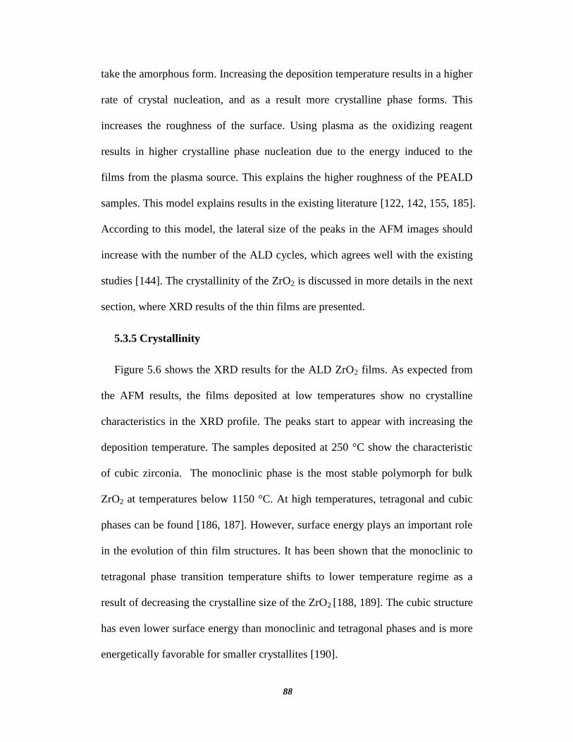
88
take the amorphous form. Increasing the deposition temperature results in a higher
rate of crystal nucleation, and as a result more crystalline phase forms. This
increases the roughness of the surface. Using plasma as the oxidizing reagent
results in higher crystalline phase nucleation due to the energy induced to the
films from the plasma source. This explains the higher roughness of the PEALD
samples. This model explains results in the existing literature [122, 142, 155, 185].
According to this model, the lateral size of the peaks in the AFM images should
increase with the number of the ALD cycles, which agrees well with the existing
studies [144]. The crystallinity of the ZrO2 is discussed in more details in the next
section, where XRD results of the thin films are presented.
5.3.5 Crystallinity
Figure 5.6 shows the XRD results for the ALD ZrO2 films. As expected from
the AFM results, the films deposited at low temperatures show no crystalline
characteristics in the XRD profile. The peaks start to appear with increasing the
deposition temperature. The samples deposited at 250 °C show the characteristic
of cubic zirconia. The monoclinic phase is the most stable polymorph for bulk
ZrO2 at temperatures below 1150 °C. At high temperatures, tetragonal and cubic
phases can be found [186, 187]. However, surface energy plays an important role
in the evolution of thin film structures. It has been shown that the monoclinic to
tetragonal phase transition temperature shifts to lower temperature regime as a
result of decreasing the crystalline size of the ZrO2 [188, 189]. The cubic structure
has even lower surface energy than monoclinic and tetragonal phases and is more
energetically favorable for smaller crystallites [190].
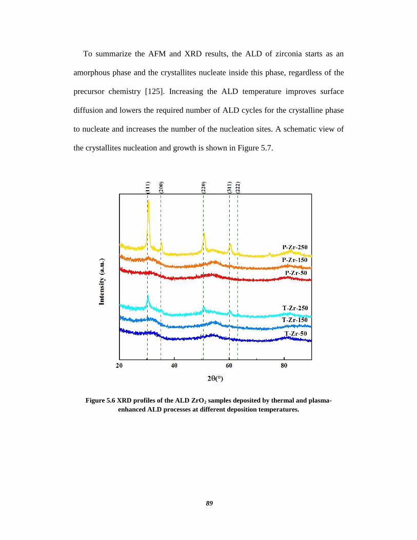
89
To summarize the AFM and XRD results, the ALD of zirconia starts as an
amorphous phase and the crystallites nucleate inside this phase, regardless of the
precursor chemistry [125]. Increasing the ALD temperature improves surface
diffusion and lowers the required number of ALD cycles for the crystalline phase
to nucleate and increases the number of the nucleation sites. A schematic view of
the crystallites nucleation and growth is shown in Figure 5.7.
Figure 5.6 XRD profiles of the ALD ZrO2 samples deposited by thermal and plasma-
enhanced ALD processes at different deposition temperatures.
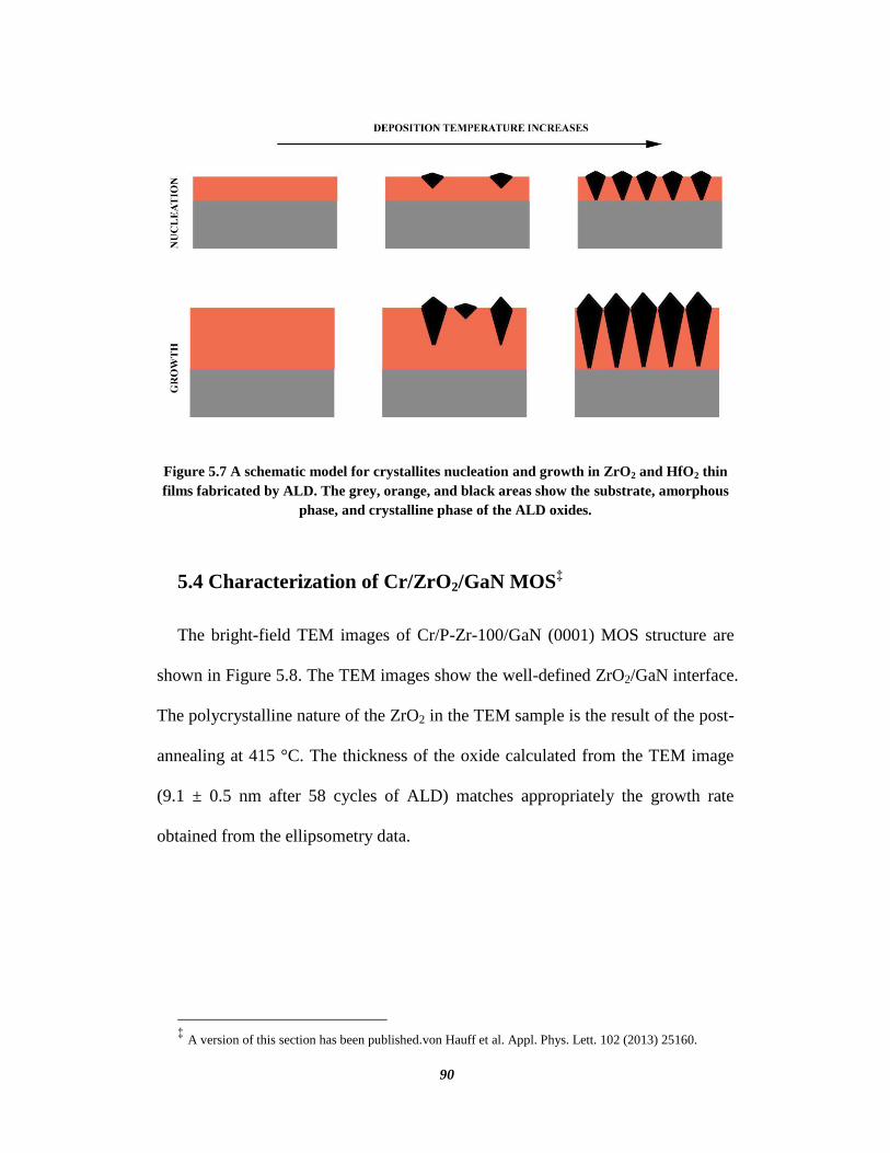
90
Figure 5.7 A schematic model for crystallites nucleation and growth in ZrO2 and HfO2 thin
films fabricated by ALD. The grey, orange, and black areas show the substrate, amorphous
phase, and crystalline phase of the ALD oxides.
5.4 Characterization of Cr/ZrO2/GaN MOS‡
The bright-field TEM images of Cr/P-Zr-100/GaN (0001) MOS structure are
shown in Figure 5.8. The TEM images show the well-defined ZrO2/GaN interface.
The polycrystalline nature of the ZrO2 in the TEM sample is the result of the post-
annealing at 415 °C. The thickness of the oxide calculated from the TEM image
(9.1 ± 0.5 nm after 58 cycles of ALD) matches appropriately the growth rate
obtained from the ellipsometry data.
‡ A version of this section has been published.von Hauff et al. Appl. Phys. Lett. 102 (2013) 25160.
91
Figure 5.8 TEM image of Cr/ZrO2/GaN MOS structure revealing the polycrystalline
microstructure of ZrO2 and the quality of the ZrO2/GaN interface.
The C-V characteristic of the MOSCAPs is represented in Figure 5.9. The raw
data is treated by transformation of a circular distributed capacitance model [159].
The hysteresis in the C-V measurements is 6mV at 20 kHz. The interface trap
density, Dit, is calculated from equation 5.1 [191].
(5.1)
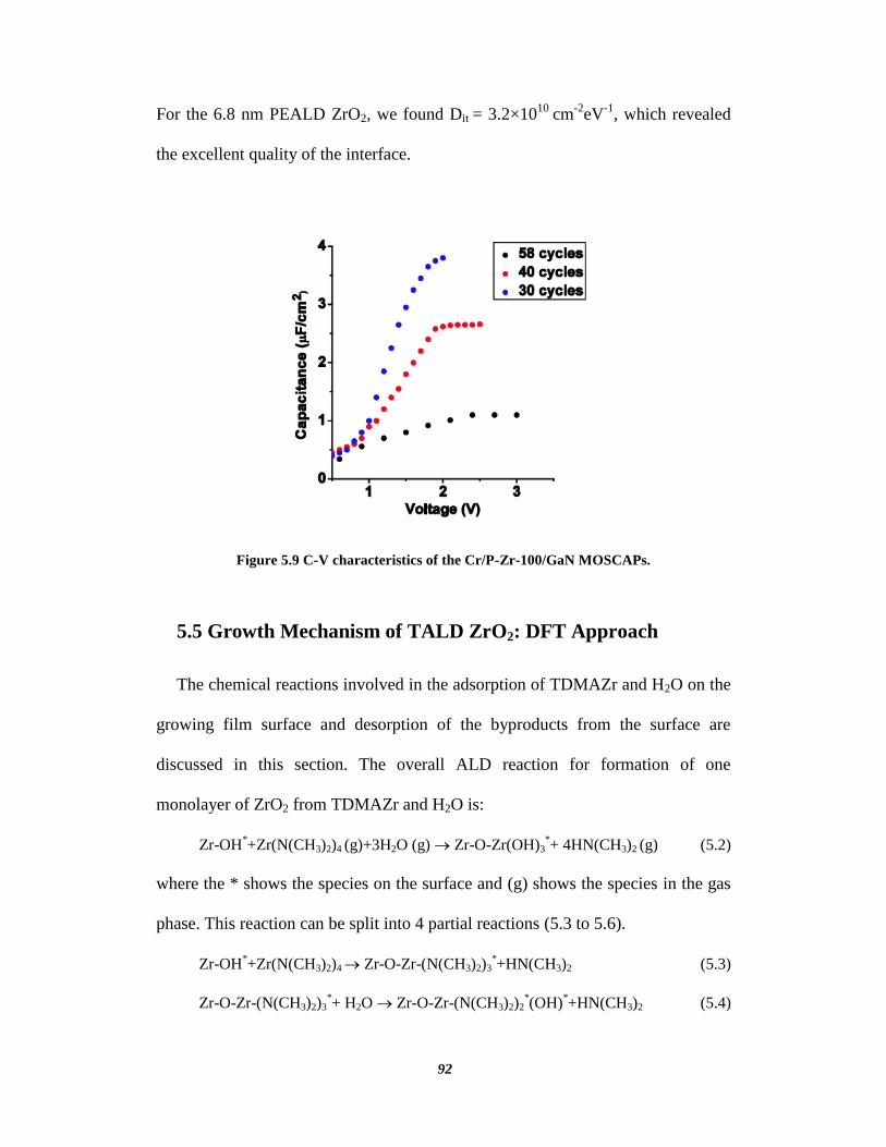
92
For the 6.8 nm PEALD ZrO2, we found Dit = 3.2×10¹⁰
cm-2
eV-1
, which revealed
the excellent quality of the interface.
Figure 5.9 C-V characteristics of the Cr/P-Zr-100/GaN MOSCAPs.
5.5 Growth Mechanism of TALD ZrO2: DFT Approach
The chemical reactions involved in the adsorption of TDMAZr and H2O on the
growing film surface and desorption of the byproducts from the surface are
discussed in this section. The overall ALD reaction for formation of one
monolayer of ZrO2 from TDMAZr and H2O is:
Zr-OH*+Zr(N(CH3)2)4 (g)+3H2O (g) Zr-O-Zr(OH)3
*+ 4HN(CH3)2 (g) (5.2)
where the * shows the species on the surface and (g) shows the species in the gas
phase. This reaction can be split into 4 partial reactions (5.3 to 5.6).
Zr-OH*+Zr(N(CH3)2)4 Zr-O-Zr-(N(CH3)2)3
*+HN(CH3)2 (5.3)
Zr-O-Zr-(N(CH3)2)3*+ H2O Zr-O-Zr-(N(CH3)2)2
*(OH)
*+HN(CH3)2 (5.4)
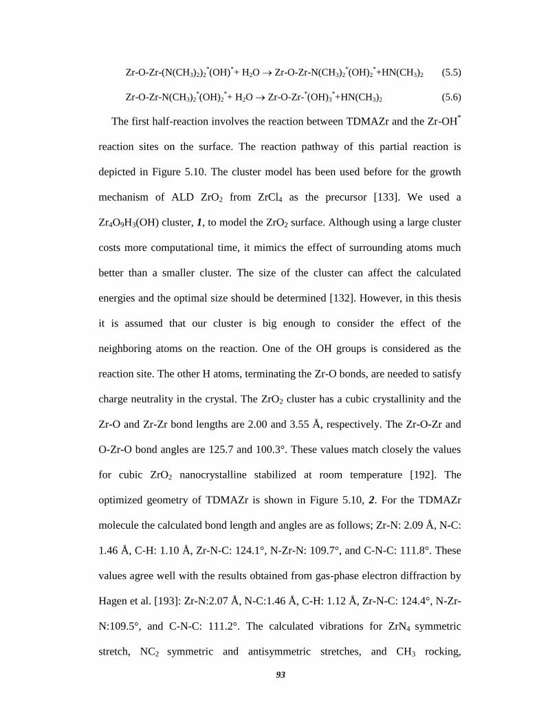
93
Zr-O-Zr-(N(CH3)2)2*(OH)
*+ H2O Zr-O-Zr-N(CH3)2
*(OH)2
*+HN(CH3)2 (5.5)
Zr-O-Zr-N(CH3)2*(OH)2
*+ H2O Zr-O-Zr-
*(OH)3
*+HN(CH3)2 (5.6)
The first half-reaction involves the reaction between TDMAZr and the Zr-OH*
reaction sites on the surface. The reaction pathway of this partial reaction is
depicted in Figure 5.10. The cluster model has been used before for the growth
mechanism of ALD ZrO2 from ZrCl4 as the precursor [133]. We used a
Zr4O9H3(OH) cluster, 1, to model the ZrO2 surface. Although using a large cluster
costs more computational time, it mimics the effect of surrounding atoms much
better than a smaller cluster. The size of the cluster can affect the calculated
energies and the optimal size should be determined [132]. However, in this thesis
it is assumed that our cluster is big enough to consider the effect of the
neighboring atoms on the reaction. One of the OH groups is considered as the
reaction site. The other H atoms, terminating the Zr-O bonds, are needed to satisfy
charge neutrality in the crystal. The ZrO2 cluster has a cubic crystallinity and the
Zr-O and Zr-Zr bond lengths are 2.00 and 3.55 Å, respectively. The Zr-O-Zr and
O-Zr-O bond angles are 125.7 and 100.3°. These values match closely the values
for cubic ZrO2 nanocrystalline stabilized at room temperature [192]. The
optimized geometry of TDMAZr is shown in Figure 5.10, 2. For the TDMAZr
molecule the calculated bond length and angles are as follows; Zr-N: 2.09 Å, N-C:
1.46 Å, C-H: 1.10 Å, Zr-N-C: 124.1°, N-Zr-N: 109.7°, and C-N-C: 111.8°. These
values agree well with the results obtained from gas-phase electron diffraction by
Hagen et al. [193]: Zr-N:2.07 Å, N-C:1.46 Å, C-H: 1.12 Å, Zr-N-C: 124.4°, N-Zr-
N:109.5°, and C-N-C: 111.2°. The calculated vibrations for ZrN4 symmetric
stretch, NC2 symmetric and antisymmetric stretches, and CH3 rocking,
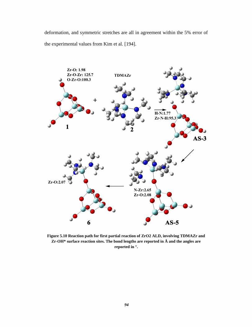
94
deformation, and symmetric stretches are all in agreement within the 5% error of
the experimental values from Kim et al. [194].
Figure 5.10 Reaction path for first partial reaction of ZrO2 ALD, involving TDMAZr and
Zr-OH* surface reaction sites. The bond lengths are reported in Å and the angles are
reported in °.
95
Figure 5.11 PES of the first partial reaction of the ALD ZrO2, between TDMAZr and –OH
surface reaction sites.
The potential energy surface (PES) of the first partial reaction is shown in
Figure 5.11. The reaction starts by adsorption of TDMAZr on the surface, AS-3.
The –OH group on the surface points towards one of the N atoms in TDMAZr.
The N-H distance is 1.77 Å and the O-H bond stretches from 0.96 Å to 1.00 Å.
This is an indication of the formation of a hydrogen bond between H in –OH* and
N in TDMAZr. The calculated adsorption energy is 4.5 kcal/mol. The adsorption
energy value and the N-H distance are very close to reported values for the
OH…N hydrogen bond [195]. Unfortunately, the geometry calculations for the
transition structure did not converge. However, from the post-transition structure
it is deduced that the reaction continues by proton transfer, H+, from –OH
* to the
N in the transition state, TS-4. In the post-transition state, AS-5, the HN(CH3)2
formed and adsorbed on the surface. This structure is located 28.2 kcal/mol lower
than the reactants on the PES. The N atom in adsorbed HN(CH3)2 points towards
the Zr at a distance of 2.65 Å. A bond is formed between O on the surface and the
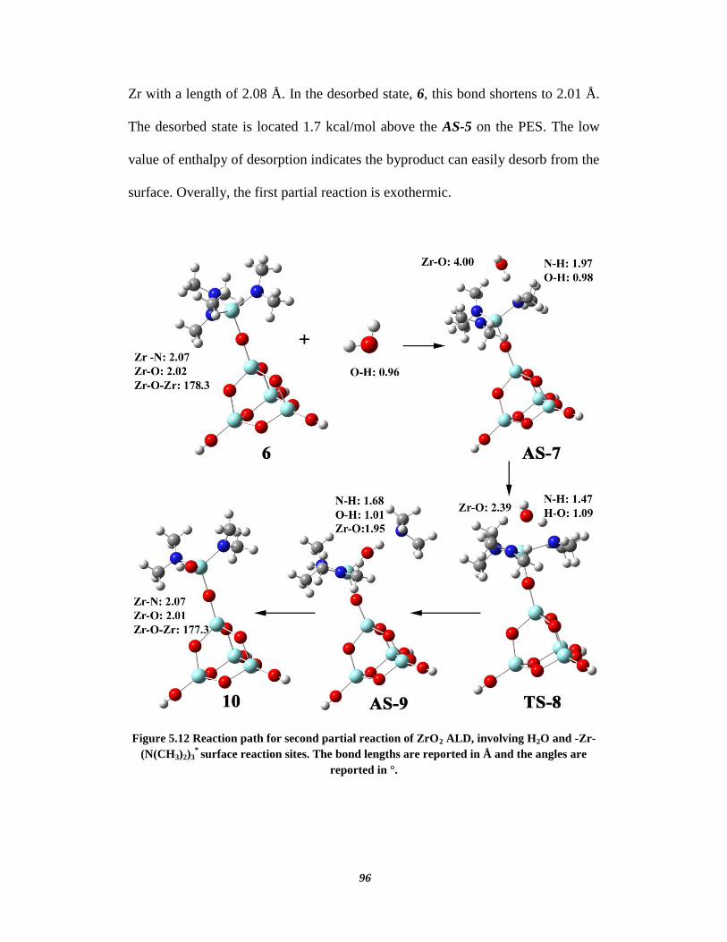
96
Zr with a length of 2.08 Å. In the desorbed state, 6, this bond shortens to 2.01 Å.
The desorbed state is located 1.7 kcal/mol above the AS-5 on the PES. The low
value of enthalpy of desorption indicates the byproduct can easily desorb from the
surface. Overally, the first partial reaction is exothermic.
Figure 5.12 Reaction path for second partial reaction of ZrO2 ALD, involving H2O and -Zr-
(N(CH3)2)3* surface reaction sites. The bond lengths are reported in Å and the angles are
reported in °.
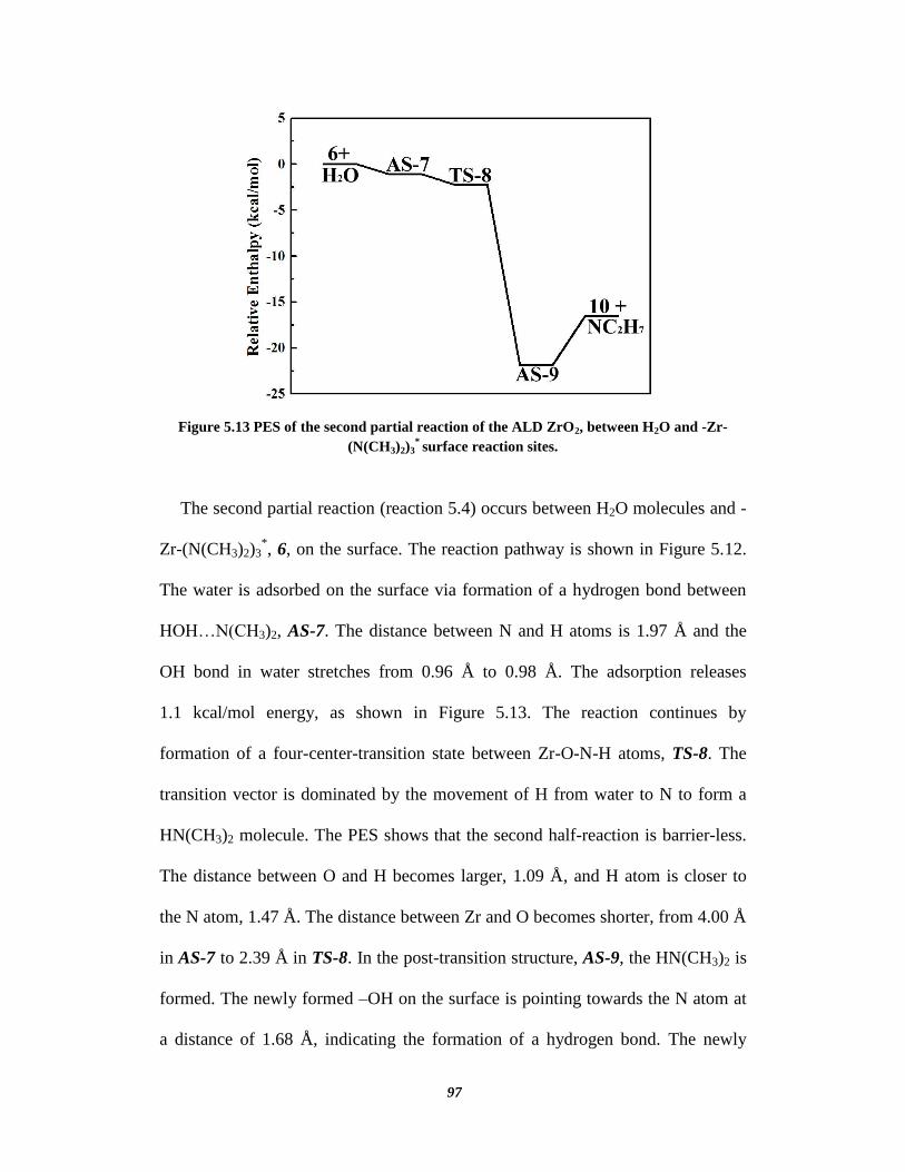
97
Figure 5.13 PES of the second partial reaction of the ALD ZrO2, between H2O and -Zr-
(N(CH3)2)3* surface reaction sites.
The second partial reaction (reaction 5.4) occurs between H2O molecules and -
Zr-(N(CH3)2)3*, 6, on the surface. The reaction pathway is shown in Figure 5.12.
The water is adsorbed on the surface via formation of a hydrogen bond between
HOH…N(CH3)2, AS-7. The distance between N and H atoms is 1.97 Å and the
OH bond in water stretches from 0.96 Å to 0.98 Å. The adsorption releases
1.1 kcal/mol energy, as shown in Figure 5.13. The reaction continues by
formation of a four-center-transition state between Zr-O-N-H atoms, TS-8. The
transition vector is dominated by the movement of H from water to N to form a
HN(CH3)2 molecule. The PES shows that the second half-reaction is barrier-less.
The distance between O and H becomes larger, 1.09 Å, and H atom is closer to
the N atom, 1.47 Å. The distance between Zr and O becomes shorter, from 4.00 Å
in AS-7 to 2.39 Å in TS-8. In the post-transition structure, AS-9, the HN(CH3)2 is
formed. The newly formed –OH on the surface is pointing towards the N atom at
a distance of 1.68 Å, indicating the formation of a hydrogen bond. The newly
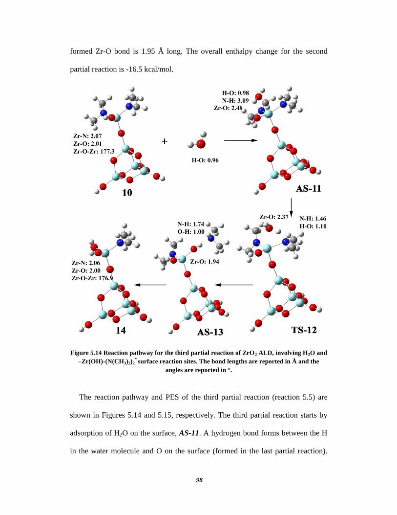
98
formed Zr-O bond is 1.95 Å long. The overall enthalpy change for the second
partial reaction is -16.5 kcal/mol.
Figure 5.14 Reaction pathway for the third partial reaction of ZrO2 ALD, involving H2O and
–Zr(OH)-(N(CH3)2)2* surface reaction sites. The bond lengths are reported in Å and the
angles are reported in °.
The reaction pathway and PES of the third partial reaction (reaction 5.5) are
shown in Figures 5.14 and 5.15, respectively. The third partial reaction starts by
adsorption of H2O on the surface, AS-11. A hydrogen bond forms between the H
in the water molecule and O on the surface (formed in the last partial reaction).
99
The enthalpy change is -4.9 kcal/mol, which is higher than the same reaction in
the second partial reaction. It seems that another weak hydrogen bond formed
between the other H in the water and the one of the N on the surface. The distance
between the O in H2O and Zr on the surface is 2.48 Å. This distance shortens to
2.37 Å in the transition state, TS-12. The water molecule rotates and the N-H
distance becomes shorter, from 3.09 to 1.46 Å. The four-center transition state is
formed between N-H-O-Zr and movement of H from water to N dominates the
transition vector. The transition state is 2.5kcal/mol above the AS-11 but is still
2.4 kcal/mol lower than the reactants. The post-transition state, AS-13, is located
22.6 kcal/mol lower than reactants on the PES. A hydrogen bond is formed
between newly formed OH on the surface and HN(CH3)2 molecules, as the OH
points towards the N at a distance of 1.74 Å. Desorption of the byproduct from the
surface is endothermic, 6.3 kcal/mol. However, the total enthalpy change for the
third partial reaction is -16.3 kcal/mol. The Zr-O bond length is 2.00 Å in the
byproduct on the surface, 14.
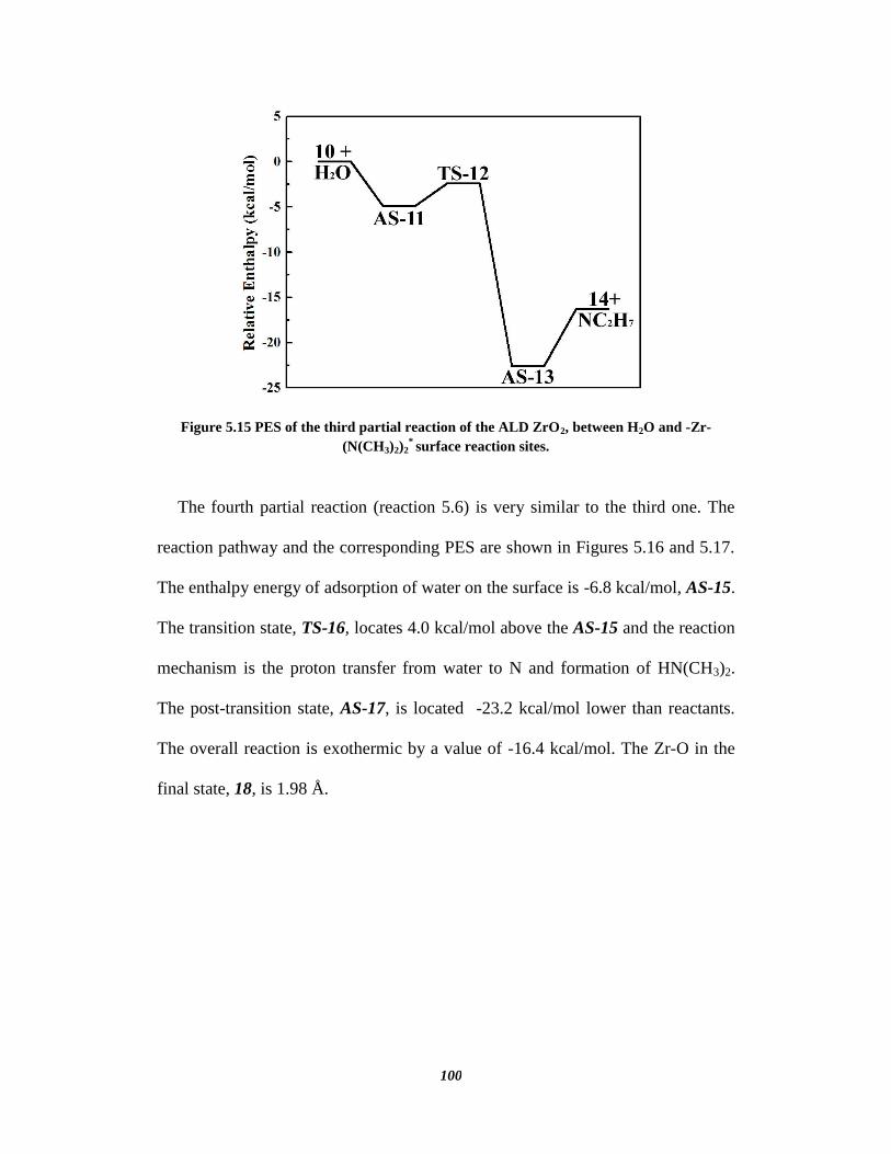
100
Figure 5.15 PES of the third partial reaction of the ALD ZrO2, between H2O and -Zr-
(N(CH3)2)2* surface reaction sites.
The fourth partial reaction (reaction 5.6) is very similar to the third one. The
reaction pathway and the corresponding PES are shown in Figures 5.16 and 5.17.
The enthalpy energy of adsorption of water on the surface is -6.8 kcal/mol, AS-15.
The transition state, TS-16, locates 4.0 kcal/mol above the AS-15 and the reaction
mechanism is the proton transfer from water to N and formation of HN(CH3)2.
The post-transition state, AS-17, is located -23.2 kcal/mol lower than reactants.
The overall reaction is exothermic by a value of -16.4 kcal/mol. The Zr-O in the
final state, 18, is 1.98 Å.

101
Figure 5.16 Reaction path for fourth partial reaction of ZrO2 ALD, involving H2O and –
Zr(OH)2-N(CH3)2* surface reaction sites. The bond lengths are reported in Å and the angles
are reported in °.
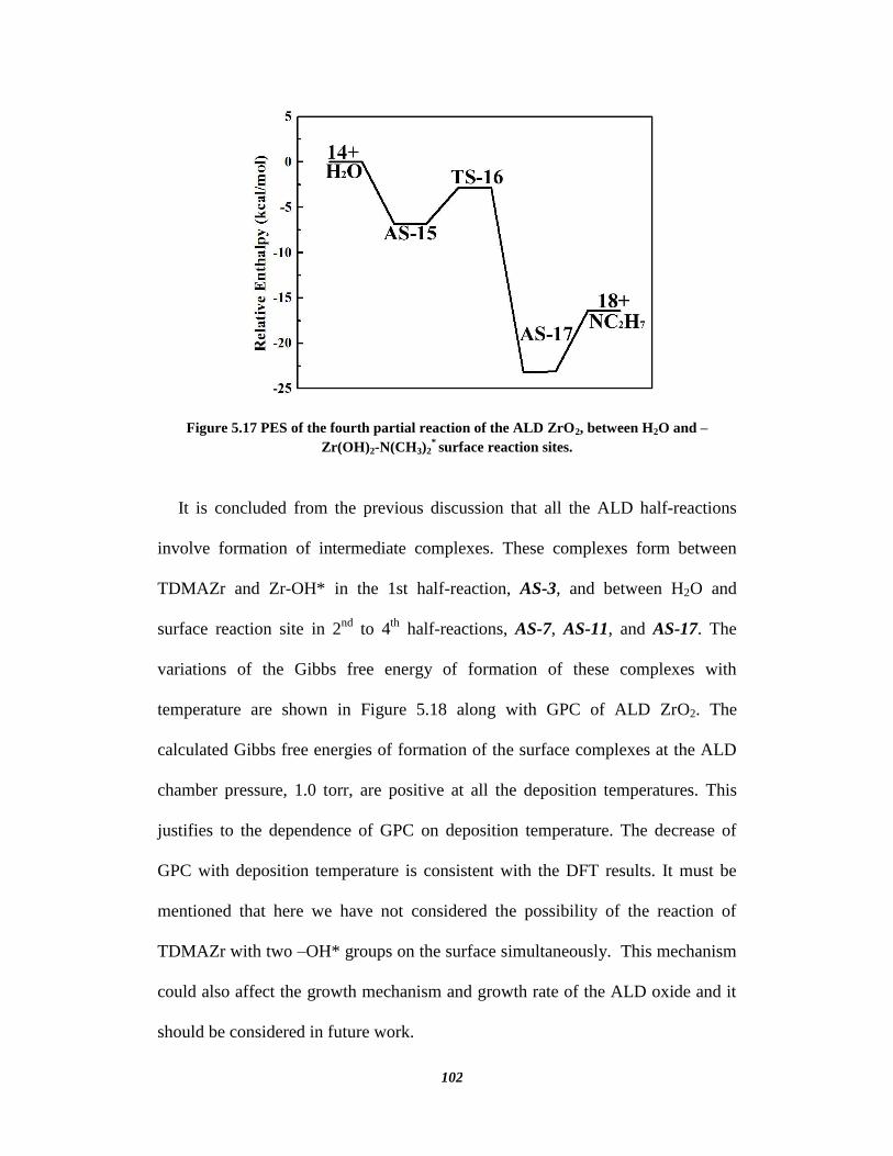
102
Figure 5.17 PES of the fourth partial reaction of the ALD ZrO2, between H2O and –
Zr(OH)2-N(CH3)2* surface reaction sites.
It is concluded from the previous discussion that all the ALD half-reactions
involve formation of intermediate complexes. These complexes form between
TDMAZr and Zr-OH* in the 1st half-reaction, AS-3, and between H2O and
surface reaction site in 2nd
to 4th
half-reactions, AS-7, AS-11, and AS-17. The
variations of the Gibbs free energy of formation of these complexes with
temperature are shown in Figure 5.18 along with GPC of ALD ZrO2. The
calculated Gibbs free energies of formation of the surface complexes at the ALD
chamber pressure, 1.0 torr, are positive at all the deposition temperatures. This
justifies to the dependence of GPC on deposition temperature. The decrease of
GPC with deposition temperature is consistent with the DFT results. It must be
mentioned that here we have not considered the possibility of the reaction of
TDMAZr with two –OH* groups on the surface simultaneously. This mechanism
could also affect the growth mechanism and growth rate of the ALD oxide and it
should be considered in future work.
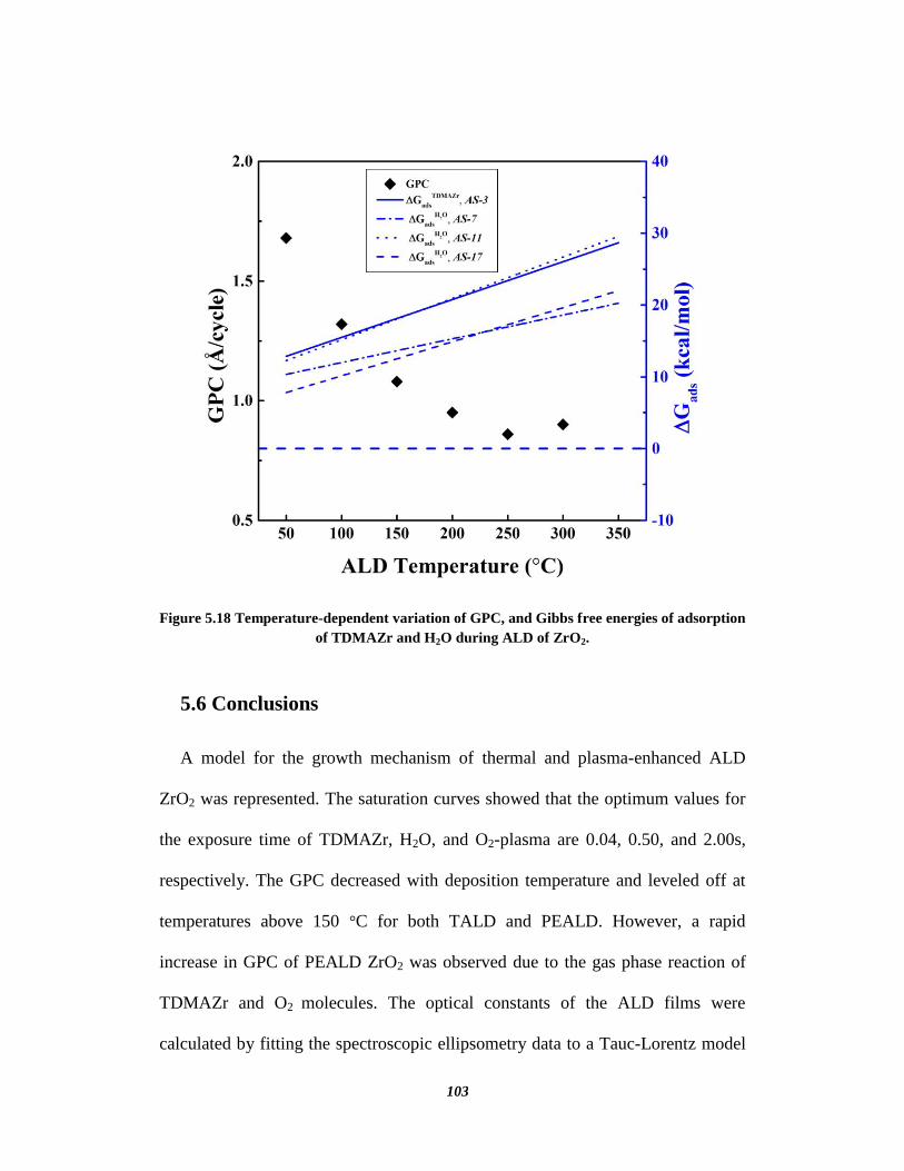
103
Figure 5.18 Temperature-dependent variation of GPC, and Gibbs free energies of adsorption
of TDMAZr and H2O during ALD of ZrO2.
5.6 Conclusions
A model for the growth mechanism of thermal and plasma-enhanced ALD
ZrO2 was represented. The saturation curves showed that the optimum values for
the exposure time of TDMAZr, H2O, and O2-plasma are 0.04, 0.50, and 2.00s,
respectively. The GPC decreased with deposition temperature and leveled off at
temperatures above 150 °C for both TALD and PEALD. However, a rapid
increase in GPC of PEALD ZrO2 was observed due to the gas phase reaction of
TDMAZr and O2 molecules. The optical constants of the ALD films were
calculated by fitting the spectroscopic ellipsometry data to a Tauc-Lorentz model
104
and agreed with the bulk values at the deposition temperatures. The optical
bandgaps for the samples were approximately 5.0 eV at all the deposition
temperatures with a slight drop at higher temperatures. The AFM studies showed
that the roughness of the ZrO2 thin films increases with the deposition
temperature due to formation of crystallites. The XRD results showed that the
crystallites have a cubic crystal structure. Based on these results, a model for the
growth of ALD ZrO2 films was proposed. The TEM images revealed the well-
defined nature of the GaN/ZrO2 interface. The density of interface trap states was
shown to be 3.2×10⁻¹⁰
cm-2
eV-1
by the C-V measurements. The chemical
compositions of the thin films were studied with XPS. It was found that ALD
ZrO2 was free from any N contamination. The amount of C in the samples varied
from 2.0 to 9.8 at.% depending on the deposition temperature. The PEALD
contained higher amount of carbon due to decomposition of TDMAZr. A DFT
approach to the growth mechanism of TALD ZrO2 was represented.
105
Chapter 6
Atomic Layer Deposition of Hafnium Oxide
6.1 Introduction
Hafnium oxide (HfO2) has a high dielectric constant of 22-25 and a large
bandgap of 5.5-6.0 eV [196, 197]. It is more stable than SiO2 (-53 kcal/mol higher
heat of formation) and it has 1.48 eV and 3.04 eV barrier heights at the interface
with Si for conductance and valence bands, respectively [196]. Hafnia also has
good thermal and chemical stability with Si [198]. These properties made HfO2 an
ideal gate oxide to replace SiO2 in MOSFETs (Metal-Oxide-Semiconductor Field-
Effect-Transistors), which are the main components of the CMOS
(complementary metal oxide semiconductor) devices [139]. HfO2 is already used
in 32-nm (2nd
Generation Gate-Last High-k Metal Gate) and 22-nm (First to
Implement Tri-Gate) Intel transistors [199]. HfO2 has been studied as the gate
material for the enhanced channel mobility MOSFETs, using III-V
semiconductors such as GaN [200, 201]. The conduction and valence band offsets
for HfO2/GaN are 1.1 and 1.6 eV, respectively and the conduction band offset for
HfO2/ZnO is 2.2 eV [27].
ALD of HfO2 has been performed using different precursor materials. Hafnium
halides (HfCl4 and HfI4) were used successfully to grow HfO2 at high deposition
temperatures (330-500 °C) [202, 203]. However, using halides as the precursor
resulted in highly crystalline films, which are not favorable because of high
leakage current [144, 204-206]. The crystalline nature of the ALD HfO2 using
106
halides was attributed to the high deposition temperature of the process. ALD
using halides at low deposition temperatures showed high level of impurities in
the films [207]. ALD of HfO2 using anhydrous hafnium nitrate (Hf(NO3)4) also
needs post-annealing at temperatures above 400 °C to remove NO3 and NO2
contaminations [208]. Consequently, complex metalorganics precursors have been
studied for HfO2 ALD as a route to low deposition temperatures [154, 209, 210].
Metal amides are highly reactive and can react at temperatures as low as 50 °C
[122]. They have high vapor pressure needed for atomic layer deposition [211,
212]. The ALD of HfO2 using three different alkylamide precursors
(tetrakis(dimethylamido) hafnium (TDMAHf), tetrakis(diethylamido) hafnium
(TDEAHf) , and tetrakis(ethylmethylamido)hafnium (TEMAHf)) were studied by
Hausmann et al. [155], and found to be self-limiting and to enable low deposition
temperatures. Kukli et al. [213, 214] performed an extensive study on the ALD of
HfO2 using TEMAHf and TDMAHf precursors at deposition temperatures above
200 °C. Deshpande et al. [215] used water and TDMAHf at temperatures between
250-350 °C to grow ALD HfO2. Ozone and oxygen plasma have been to replace
water as the oxidizing agent for the deposition of HfO2 at T>200 °C [216, 217].
However, there is lack of studies on ALD HfO2 using alkylamides at low
deposition temperatures.
In this chapter, the thermal and plasma-enhanced ALD of HfO2 using
TDMAHf are investigated in the temperature range 50 – 300 °C. The optical
constants, chemical composition, roughness, crystallinity, and C-V characteristics
107
of the thin films are studied. An atomistic model of thermal ALD of HfO2 is
presented using density functional theory approach.
6.2 Experimental Procedure and Computational Calculations
The details of experimental procedure can be found in Chapter 3 and 5.
GAUSSIAN 09 [100] was used to perform molecular orbital calculations. The
geometry of stationary points was located using the B3LYP gradient corrected
density functional method [59-62] with 6-31+G(d,p) basis set [161-168] for
nonmetallic atoms, and Los Alamos ECP plus DZ (LanL2DZ) for Hf [169-171].
This level of theory has shown reliable results in studying growth mechanisms of
ALD HfO2 using HfCl4 and alkylamides [134, 218-220]. Frequency calculations
were carried out at the same level of theory to identify the nature of the stationary
points (local minima and transition states) and to calculate the zero-point energy
corrections and the thermal corrections at ALD temperature and pressure. All
energies reported are modified by the zero-point energy correction value.
6.3 Results
6.3.1 Optical Constants
The refractive index and extinction coefficient of TALD and PEALD HfO2 are
plotted against deposition temperature and incident photon energy in Figure 6.1.
Good agreement between these results and literature values was found [221, 222].
Both n and k increase with the deposition temperature. As expected, the refractive
indices of the films increase with deposition temperatures due to higher density.
However, a small decrease in n is observed at 350 °C due to decomposition of the
108
precursor at elevated temperatures. This is discussed further in section 6.3.3,
where the chemical composition of the films is presented. The refractive index of
the PEALD films show an abrupt variation at deposition temperatures below
100 °C. The refractive index and extinction coefficient remain roughly constant
over the deposition temperature range of 100-300 °C. The optical bandgaps of the
films deposited using the same ALD system and deposition recipes were
discussed by Foroughi [223]. It was found that the optical bandgap of the ALD
HfO2 varies from 5.4 to 5.6 eV depending on the deposition temperature and is
slightly lower than bulk values due to presence of impurities.
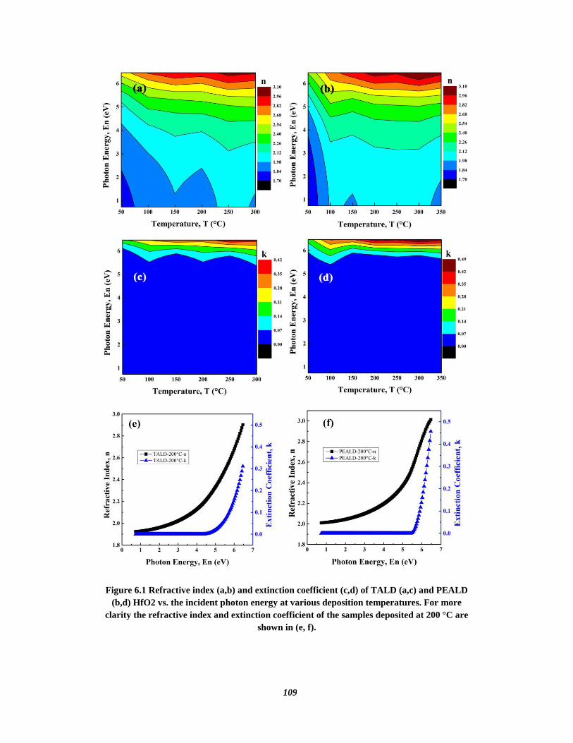
109
Figure 6.1 Refractive index (a,b) and extinction coefficient (c,d) of TALD (a,c) and PEALD
(b,d) HfO2 vs. the incident photon energy at various deposition temperatures. For more
clarity the refractive index and extinction coefficient of the samples deposited at 200 °C are
shown in (e, f).
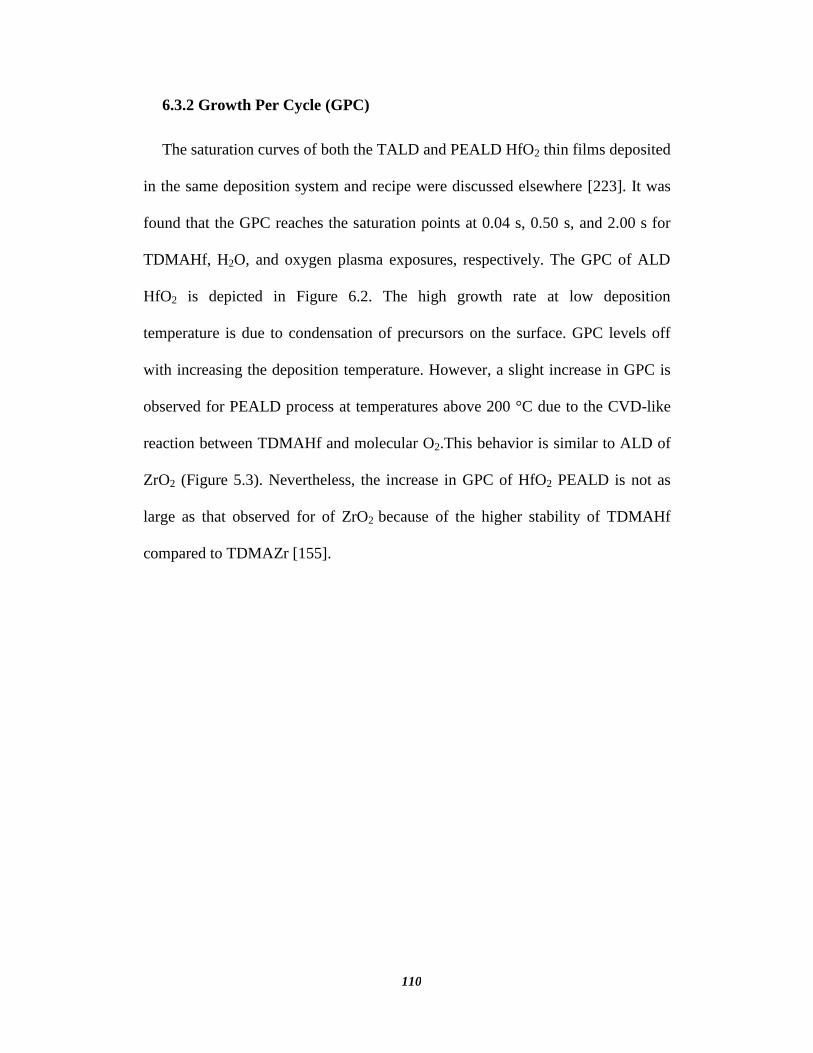
110
6.3.2 Growth Per Cycle (GPC)
The saturation curves of both the TALD and PEALD HfO2 thin films deposited
in the same deposition system and recipe were discussed elsewhere [223]. It was
found that the GPC reaches the saturation points at 0.04 s, 0.50 s, and 2.00 s for
TDMAHf, H2O, and oxygen plasma exposures, respectively. The GPC of ALD
HfO2 is depicted in Figure 6.2. The high growth rate at low deposition
temperature is due to condensation of precursors on the surface. GPC levels off
with increasing the deposition temperature. However, a slight increase in GPC is
observed for PEALD process at temperatures above 200 °C due to the CVD-like
reaction between TDMAHf and molecular O2.This behavior is similar to ALD of
ZrO2 (Figure 5.3). Nevertheless, the increase in GPC of HfO2 PEALD is not as
large as that observed for of ZrO2 because of the higher stability of TDMAHf
compared to TDMAZr [155].
111
Figure 6.2 Variation of GPC with deposition temperature for TALD and PEALD of HfO2.
6.3.3 Chemical Composition
High-resolution XPS profiles of Hf, O, C, and N elements are shown in Figure
6.3. Table 6.1 summarizes the binding energies and amount of each element in the
films. The Hf profile shows two distinct peaks at binding energies of 17.2 and
18.9 eV attributed to Hf4f7/2 and Hf4f5/2 doublets [224-226]. The intensity ratio of
these peaks agrees well with 4/3 value of theory. The spin-orbital split value i.e.
the difference between the binding energies of Hf4f7/2 and Hf4f5/2, matches the
1.66 eV reported by Kaichev et al. [184]. The ALD films at deposition
temperature of 250 °C show another peak at the binding energy of 16.4 eV related
to hafnium bonding with nitrogen [225, 227]. The appearance of this peak at
higher deposition temperature is an indication of decomposition of the precursor.
112
The O1s profile depicted in Figure 6.3b, shows the main peak at approximately
530.5 eV. This peak is attributed to Hf-O bond in HfO2 [225]. The difference
between O1s and Hf4f7/2 binding energies is 513.3 eV and agrees with the
reported value for HfO2 thin films on Si [184]. As shown in Table 6.1, the
marginal shifts of O1s and Hf4f peaks to higher binding energies indicate a
transition from suboxide to full oxide for HfO2 with increasing the deposition
temperature [228]. This also appears as the higher O/Hf ratio in Table 6.1.
However, it is worthy to recall that the preferential etching of O atoms by Ar+ ions
must be considered in treating the results [184]. The other oxygen peak at 532.1
eV can be attributed to the Hf-OH species. The intensity of this peak reduces with
increasing deposition temperature, due to desorption of the –OH from the surface
in the form of H2O.
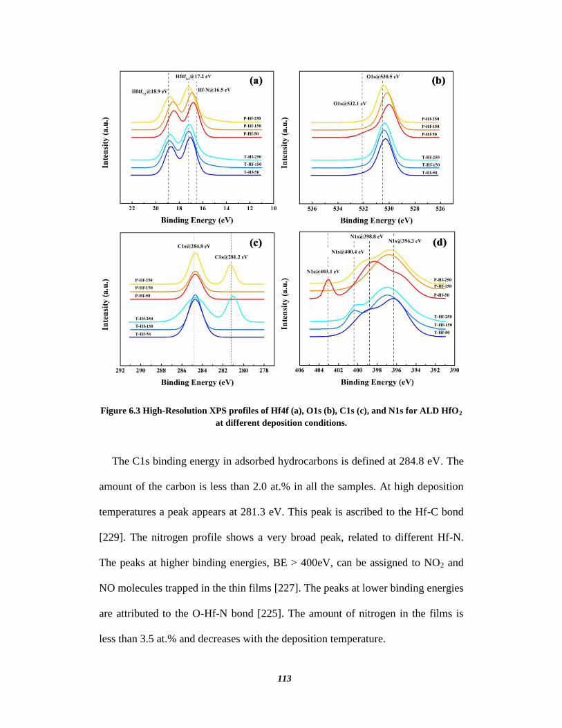
113
Figure 6.3 High-Resolution XPS profiles of Hf4f (a), O1s (b), C1s (c), and N1s for ALD HfO2
at different deposition conditions.
The C1s binding energy in adsorbed hydrocarbons is defined at 284.8 eV. The
amount of the carbon is less than 2.0 at.% in all the samples. At high deposition
temperatures a peak appears at 281.3 eV. This peak is ascribed to the Hf-C bond
[229]. The nitrogen profile shows a very broad peak, related to different Hf-N.
The peaks at higher binding energies, BE > 400eV, can be assigned to NO2 and
NO molecules trapped in the thin films [227]. The peaks at lower binding energies
are attributed to the O-Hf-N bond [225]. The amount of nitrogen in the films is
less than 3.5 at.% and decreases with the deposition temperature.
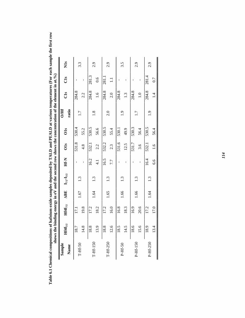
11
4
Ta
ble
6.1
Ch
em
ica
l co
mp
osi
tio
ns
of
ha
fniu
m o
xid
e sa
mp
les
dep
osi
ted
by
TA
LD
an
d P
EA
LD
at
va
rio
us
tem
per
atu
res
(Fo
r ea
ch s
am
ple
th
e fi
rst
row
sho
ws
the
bin
din
g e
ner
gy
in
eV
an
d t
he
seco
nd
ro
w s
ho
ws
the
con
cen
tra
tio
n o
f th
e el
emen
t in
at.
%)
Sa
mp
le
Na
me
Hf4
f 5/2
Hf4
f 7/2
ΔBE
I 7
/2-I
5/2
H
f-N
O
1s
O1
s O
/Hf
rati
o
C1
s C
1s
N1
s
T-H
f-5
0
18
.7
17
.1
1.6
7
1.3
-
53
1.8
5
30
.4
1.7
2
84
.8
- 3
.3
14
.8
19
.8
- 4
.8
55
.2
2.2
-
T-H
f-1
50
1
8.8
1
7.2
1
.64
1.3
1
6.2
5
32
.1
53
0.5
1
.8
28
4.8
2
81
.3
2.9
1
3.9
1
8.2
4
.1
2.2
5
6.6
1
.6
0.6
T-H
f-2
50
1
8.8
1
7.2
1
.65
1.3
1
6.5
5
32
.2
53
0.5
2
.0
28
4.8
2
81
.1
2.9
1
2.6
1
6.0
7
.7
2.3
5
5.4
2
.0
1.1
P-H
f-5
0
18
.5
16
.8
1.6
6
1.3
-
53
1.6
5
30
.1
1.9
2
84
.8
- 3
.5
14
.5
18
.3
- 1
2.5
4
9.9
1
.3
-
P-H
f-1
50
1
8.6
1
6.9
1
.66
1.3
-
53
1.7
5
30
.3
1.7
2
84
.8
- 2
.9
15
.6
20
.6
- 3
.6
56
.4
1.0
-
P-H
f-2
50
1
8.9
1
7.2
1
.64
1.3
1
6.4
5
32
.1
53
0.5
1
.9
28
4.8
2
81
.4
2.9
1
3.4
1
7.0
6
.6
1.6
5
6.4
1
.4
0.7

115
6.3.4 Roughness and Crystallinity
The roughness parameters for HfO2 thin films are reported in Table 6.2. The
AFM images are shown in Figure 6.3. The TALD samples have lower roughness
than PEALD. For both the processes, the roughness increases with the deposition
temperatures. The AFM images reveal that peaks appear on the surface of the thin
films with increasing temperatures. The number, height, and lateral size of these
peaks increase with the deposition temperature. At the same deposition
temperature, the PEALD process results in rougher surface than of TALD. These
peaks can be assigned to the crystallites in the ALD films [122]. The same model
discussed for the crystal nucleation and growth in ZrO2 ALD appears to be valid
for HfO2 as well. However, because of the stronger bonding in HfO2 (boiling
point of 5400 °C) compared to ZrO2 (4300 °C), crystal nucleation shifts to higher
temperatures.
Table 6.2 RMS Roughness of the TALD and PEALD HfO2 deposited at various
temperatures (nm) (the Si substrate roughness was 0.11 ± 0.02 nm)
Deposition Temperature (C) TALD PEALD
50
150
250
0.63 ± 0.06
0.92 ± 0.09
1.99 ± 0.12
1.41 ± 0.11
4.32 ± 0.25
8.69 ± 0.48
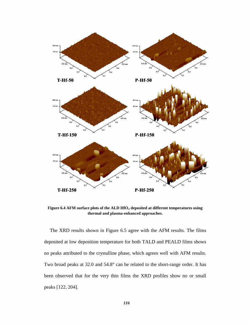
116
Figure 6.4 AFM surface plots of the ALD HfO2 deposited at different temperatures using
thermal and plasma-enhanced approaches.
The XRD results shown in Figure 6.5 agree with the AFM results. The films
deposited at low deposition temperature for both TALD and PEALD films shows
no peaks attributed to the crystalline phase, which agrees well with AFM results.
Two broad peaks at 32.0 and 54.8° can be related to the short-range order. It has
been observed that for the very thin films the XRD profiles show no or small
peaks [122, 204].
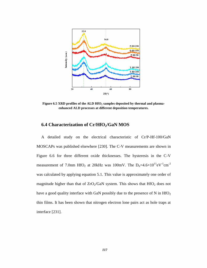
117
Figure 6.5 XRD profiles of the ALD HfO2 samples deposited by thermal and plasma-
enhanced ALD processes at different deposition temperatures.
6.4 Characterization of Cr/HfO2/GaN MOS
A detailed study on the electrical characteristic of Cr/P-Hf-100/GaN
MOSCAPs was published elsewhere [230]. The C-V measurements are shown in
Figure 6.6 for three different oxide thicknesses. The hysteresis in the C-V
measurement of 7.0nm HfO2 at 20kHz was 100mV. The Dit=4.6×10¹¹
eV-1
cm-2
was calculated by applying equation 5.1. This value is approximately one order of
magnitude higher than that of ZrO2/GaN system. This shows that HfO2 does not
have a good quality interface with GaN possibly due to the presence of N in HfO2
thin films. It has been shown that nitrogen electron lone pairs act as hole traps at
interface [231].
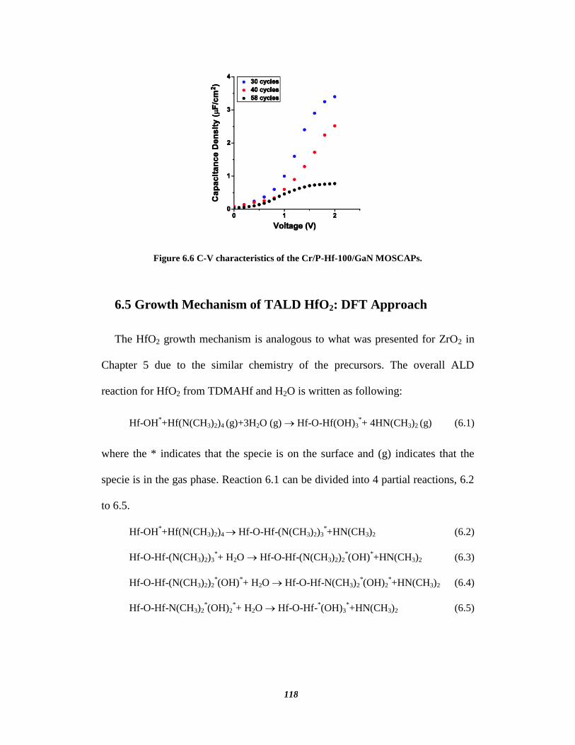
118
Figure 6.6 C-V characteristics of the Cr/P-Hf-100/GaN MOSCAPs.
6.5 Growth Mechanism of TALD HfO2: DFT Approach
The HfO2 growth mechanism is analogous to what was presented for ZrO2 in
Chapter 5 due to the similar chemistry of the precursors. The overall ALD
reaction for HfO2 from TDMAHf and H2O is written as following:
Hf-OH*+Hf(N(CH3)2)4 (g)+3H2O (g) Hf-O-Hf(OH)3
*+ 4HN(CH3)2 (g) (6.1)
where the * indicates that the specie is on the surface and (g) indicates that the
specie is in the gas phase. Reaction 6.1 can be divided into 4 partial reactions, 6.2
to 6.5.
Hf-OH*+Hf(N(CH3)2)4 Hf-O-Hf-(N(CH3)2)3
*+HN(CH3)2 (6.2)
Hf-O-Hf-(N(CH3)2)3*+ H2O Hf-O-Hf-(N(CH3)2)2
*(OH)
*+HN(CH3)2 (6.3)
Hf-O-Hf-(N(CH3)2)2*(OH)
*+ H2O Hf-O-Hf-N(CH3)2
*(OH)2
*+HN(CH3)2 (6.4)
Hf-O-Hf-N(CH3)2*(OH)2
*+ H2O Hf-O-Hf-
*(OH)3
*+HN(CH3)2 (6.5)
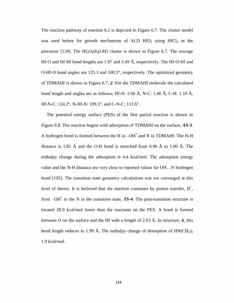
119
The reaction pathway of reaction 6.2 is depicted in Figure 6.7. The cluster model
was used before for growth mechanism of ALD HfO2 using HfCl4 as the
precursor [134]. The Hf4O9H3(OH) cluster is shown in Figure 6.7. The average
Hf-O and Hf-Hf bond lengths are 1.97 and 3.49 Å, respectively. The Hf-O-Hf and
O-Hf-O bond angles are 125.3 and 100.5°, respectively. The optimized geometry
of TDMAHf is shown in Figure 6.7, 2. For the TDMAHf molecule the calculated
bond length and angles are as follows; Hf-N: 2.06 Å, N-C: 1.46 Å, C-H: 1.10 Å,
Hf-N-C: 124.2°, N-Hf-N: 109.5°, and C-N-C: 111.6°.
The potential energy surface (PES) of the first partial reaction is shown in
Figure 6.8. The reaction begins with adsorption of TDMAHf on the surface, AS-3.
A hydrogen bond is formed between the H in –OH* and N in TDMAHf. The N-H
distance is 1.81 Å and the O-H bond is stretched from 0.96 Å to 1.00 Å. The
enthalpy change during the adsorption is 4.4 kcal/mol. The adsorption energy
value and the N-H distance are very close to reported values for OH…N hydrogen
bond [195]. The transition state geometry calculations was not converged at this
level of theory. It is believed that the reaction continues by proton transfer, H+,
from –OH* to the N in the transition state, TS-4. The post-transition structure is
located 28.9 kcal/mol lower than the reactants on the PES. A bond is formed
between O on the surface and the Hf with a length of 2.03 Å. In structure, 6, this
bond length reduces to 1.99 Å. The enthalpy change of desorption of HN(CH3)2
1.9 kcal/mol.
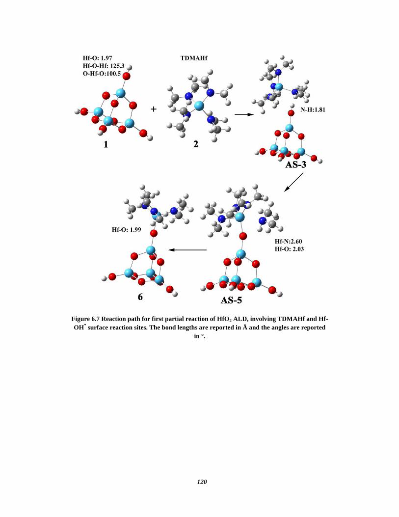
120
Figure 6.7 Reaction path for first partial reaction of HfO2 ALD, involving TDMAHf and Hf-
OH* surface reaction sites. The bond lengths are reported in Å and the angles are reported
in °.
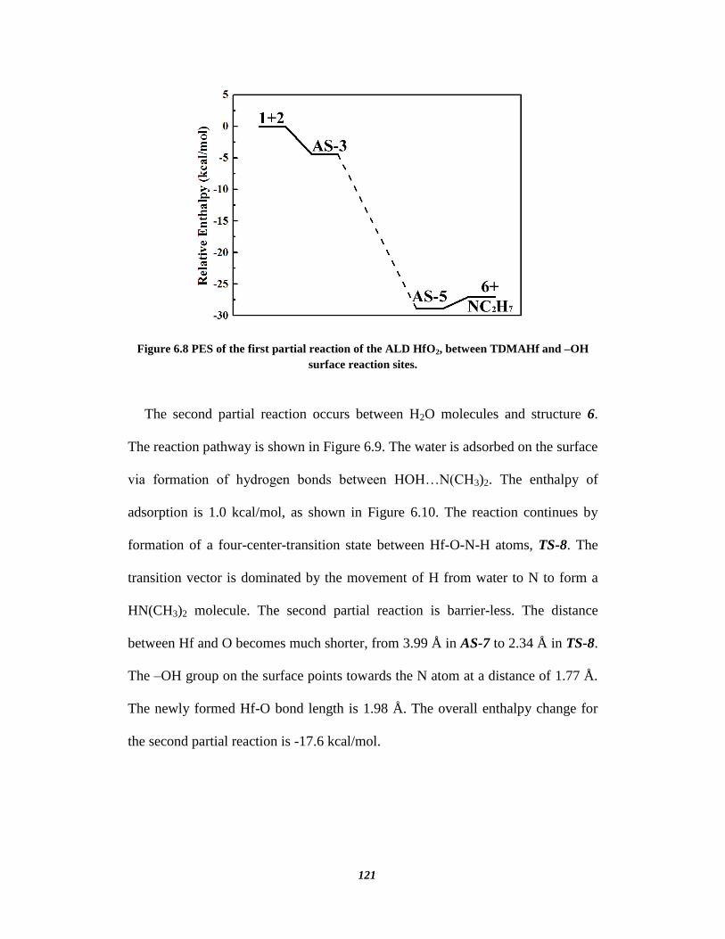
121
Figure 6.8 PES of the first partial reaction of the ALD HfO2, between TDMAHf and –OH
surface reaction sites.
The second partial reaction occurs between H2O molecules and structure 6.
The reaction pathway is shown in Figure 6.9. The water is adsorbed on the surface
via formation of hydrogen bonds between HOH…N(CH3)2. The enthalpy of
adsorption is 1.0 kcal/mol, as shown in Figure 6.10. The reaction continues by
formation of a four-center-transition state between Hf-O-N-H atoms, TS-8. The
transition vector is dominated by the movement of H from water to N to form a
HN(CH3)2 molecule. The second partial reaction is barrier-less. The distance
between Hf and O becomes much shorter, from 3.99 Å in AS-7 to 2.34 Å in TS-8.
The –OH group on the surface points towards the N atom at a distance of 1.77 Å.
The newly formed Hf-O bond length is 1.98 Å. The overall enthalpy change for
the second partial reaction is -17.6 kcal/mol.
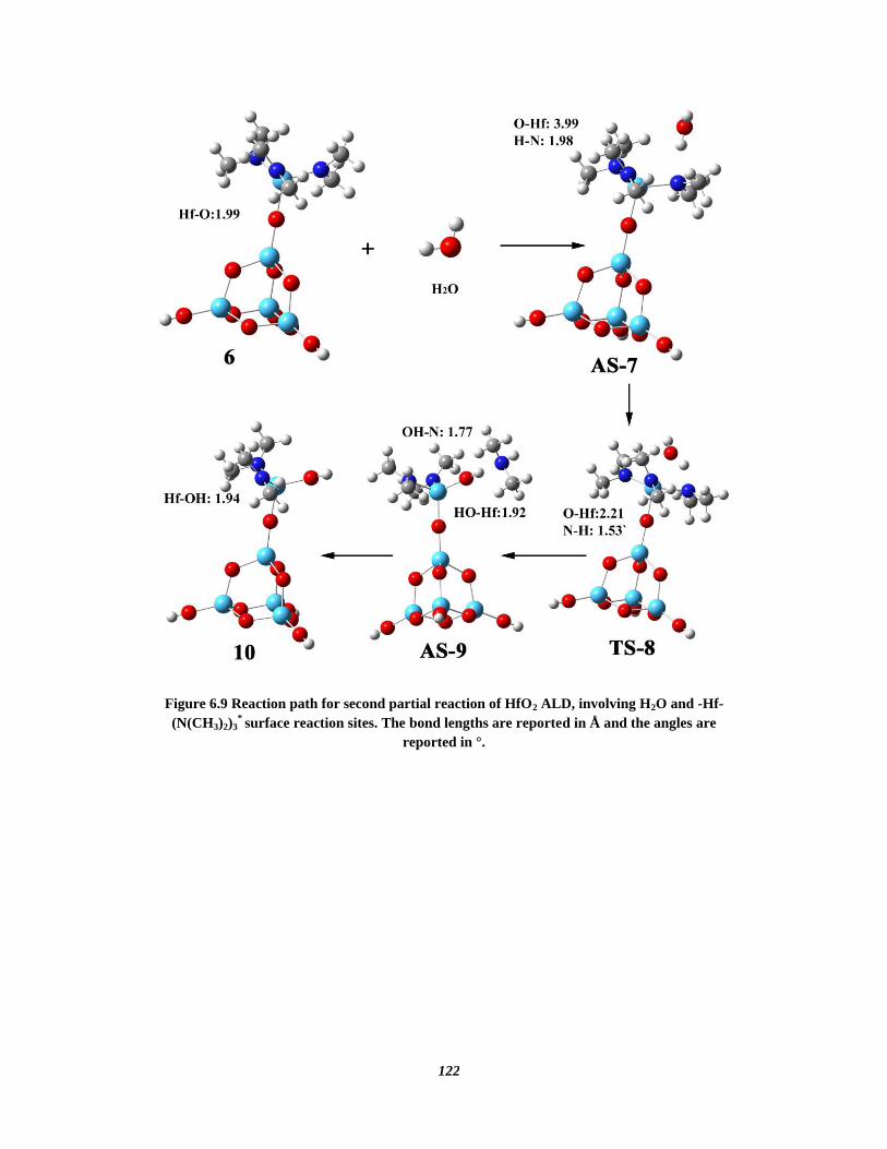
122
Figure 6.9 Reaction path for second partial reaction of HfO2 ALD, involving H2O and -Hf-
(N(CH3)2)3* surface reaction sites. The bond lengths are reported in Å and the angles are
reported in °.
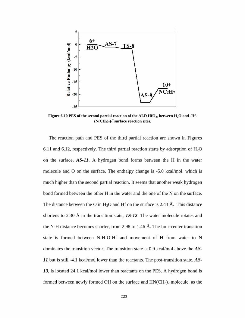
123
Figure 6.10 PES of the second partial reaction of the ALD HfO2, between H2O and -Hf-
(N(CH3)2)3* surface reaction sites.
The reaction path and PES of the third partial reaction are shown in Figures
6.11 and 6.12, respectively. The third partial reaction starts by adsorption of H2O
on the surface, AS-11. A hydrogen bond forms between the H in the water
molecule and O on the surface. The enthalpy change is -5.0 kcal/mol, which is
much higher than the second partial reaction. It seems that another weak hydrogen
bond formed between the other H in the water and the one of the N on the surface.
The distance between the O in H2O and Hf on the surface is 2.43 Å. This distance
shortens to 2.30 Å in the transition state, TS-12. The water molecule rotates and
the N-H distance becomes shorter, from 2.98 to 1.46 Å. The four-center transition
state is formed between N-H-O-Hf and movement of H from water to N
dominates the transition vector. The transition state is 0.9 kcal/mol above the AS-
11 but is still -4.1 kcal/mol lower than the reactants. The post-transition state, AS-
13, is located 24.1 kcal/mol lower than reactants on the PES. A hydrogen bond is
formed between newly formed OH on the surface and HN(CH3)2 molecule, as the
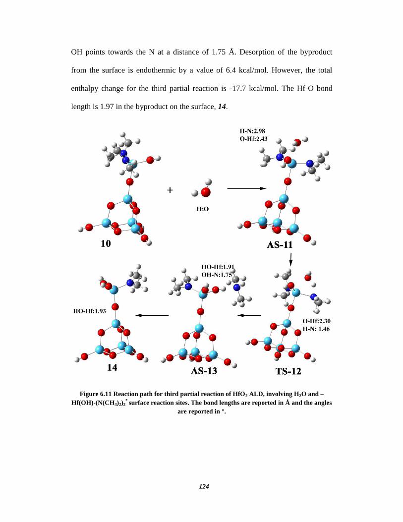
124
OH points towards the N at a distance of 1.75 Å. Desorption of the byproduct
from the surface is endothermic by a value of 6.4 kcal/mol. However, the total
enthalpy change for the third partial reaction is -17.7 kcal/mol. The Hf-O bond
length is 1.97 in the byproduct on the surface, 14.
Figure 6.11 Reaction path for third partial reaction of HfO2 ALD, involving H2O and –
Hf(OH)-(N(CH3)2)2* surface reaction sites. The bond lengths are reported in Å and the angles
are reported in °.
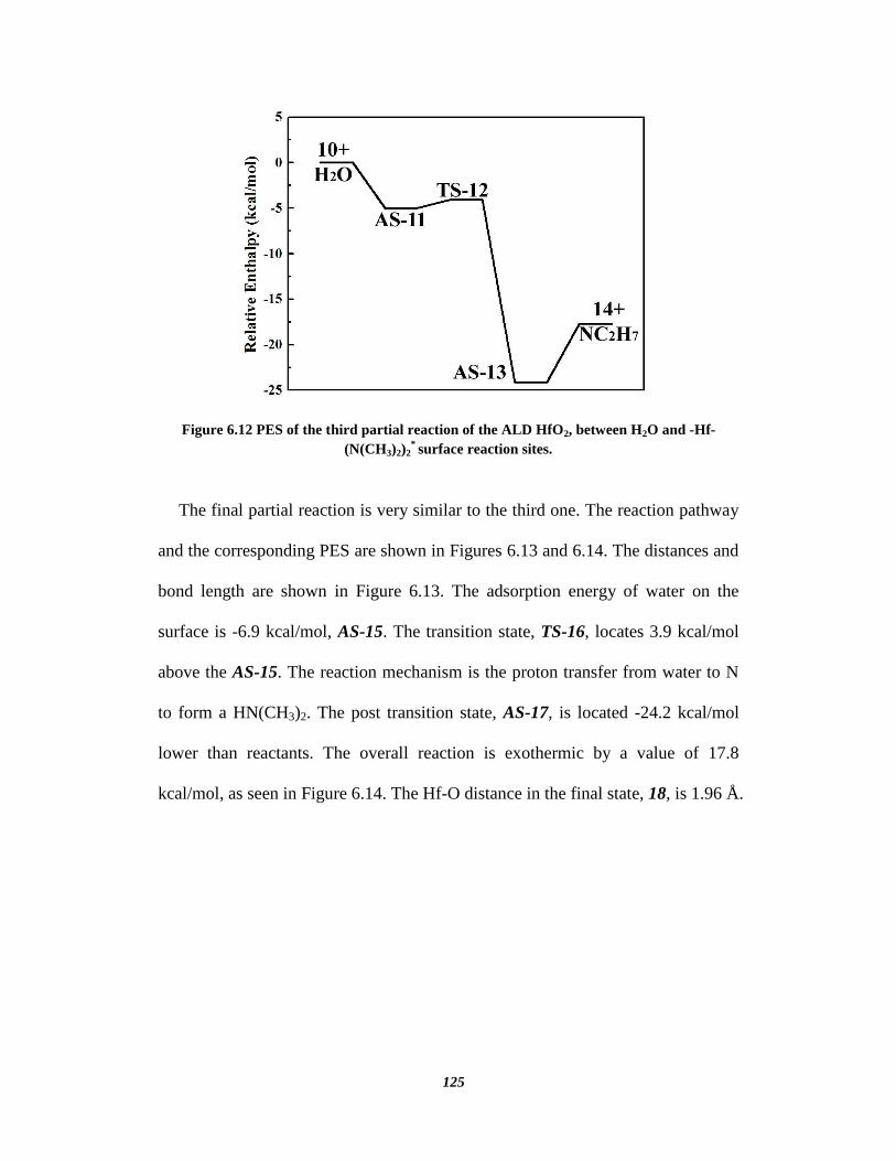
125
Figure 6.12 PES of the third partial reaction of the ALD HfO2, between H2O and -Hf-
(N(CH3)2)2* surface reaction sites.
The final partial reaction is very similar to the third one. The reaction pathway
and the corresponding PES are shown in Figures 6.13 and 6.14. The distances and
bond length are shown in Figure 6.13. The adsorption energy of water on the
surface is -6.9 kcal/mol, AS-15. The transition state, TS-16, locates 3.9 kcal/mol
above the AS-15. The reaction mechanism is the proton transfer from water to N
to form a HN(CH3)2. The post transition state, AS-17, is located -24.2 kcal/mol
lower than reactants. The overall reaction is exothermic by a value of 17.8
kcal/mol, as seen in Figure 6.14. The Hf-O distance in the final state, 18, is 1.96 Å.
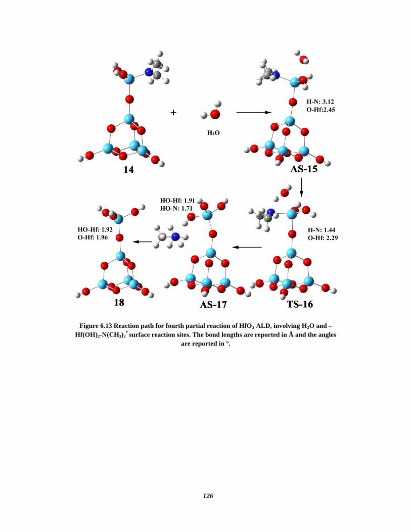
126
Figure 6.13 Reaction path for fourth partial reaction of HfO2 ALD, involving H2O and –
Hf(OH)2-N(CH3)2* surface reaction sites. The bond lengths are reported in Å and the angles
are reported in °.
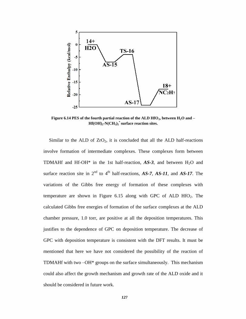
127
Figure 6.14 PES of the fourth partial reaction of the ALD HfO2, between H2O and –
Hf(OH)2-N(CH3)2* surface reaction sites.
Similar to the ALD of ZrO2, it is concluded that all the ALD half-reactions
involve formation of intermediate complexes. These complexes form between
TDMAHf and Hf-OH* in the 1st half-reaction, AS-3, and between H2O and
surface reaction site in 2nd
to 4th
half-reactions, AS-7, AS-11, and AS-17. The
variations of the Gibbs free energy of formation of these complexes with
temperature are shown in Figure 6.15 along with GPC of ALD HfO2. The
calculated Gibbs free energies of formation of the surface complexes at the ALD
chamber pressure, 1.0 torr, are positive at all the deposition temperatures. This
justifies to the dependence of GPC on deposition temperature. The decrease of
GPC with deposition temperature is consistent with the DFT results. It must be
mentioned that here we have not considered the possibility of the reaction of
TDMAHf with two –OH* groups on the surface simultaneously. This mechanism
could also affect the growth mechanism and growth rate of the ALD oxide and it
should be considered in future work.
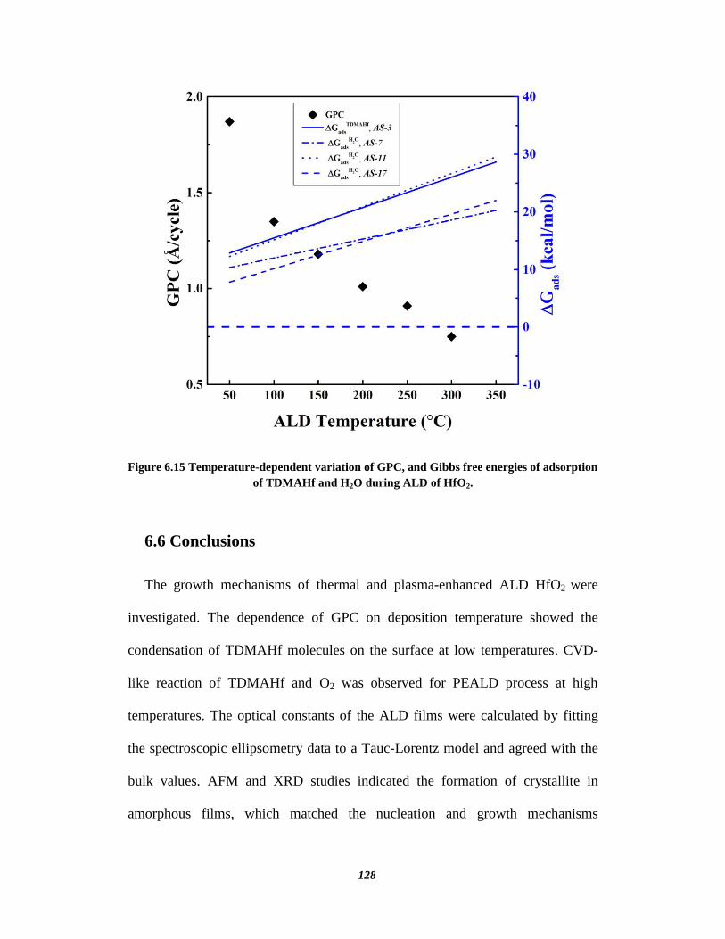
128
Figure 6.15 Temperature-dependent variation of GPC, and Gibbs free energies of adsorption
of TDMAHf and H2O during ALD of HfO2.
6.6 Conclusions
The growth mechanisms of thermal and plasma-enhanced ALD HfO2 were
investigated. The dependence of GPC on deposition temperature showed the
condensation of TDMAHf molecules on the surface at low temperatures. CVD-
like reaction of TDMAHf and O2 was observed for PEALD process at high
temperatures. The optical constants of the ALD films were calculated by fitting
the spectroscopic ellipsometry data to a Tauc-Lorentz model and agreed with the
bulk values. AFM and XRD studies indicated the formation of crystallite in
amorphous films, which matched the nucleation and growth mechanisms

129
proposed for ALD of ZrO2. The density of interface trap states was shown to be
an order of magnitude higher than that of ZrO2/GaN interface. This can be
attributed to the presence of N impurities in the HfO2 thin films. However, the
amount of C in the samples was less than 3.0 at.% depending on the deposition
temperature. A DFT approach to the growth mechanism of TALD HfO2 was
represented. It was observed that the enthalpy changes and reaction pathways are
very similar to ALD of ZrO2 due to the similar chemistry of the precursors.
130
Chapter 7
Conclusions and Future Work
The purpose of this thesis is an in-depth study of growth mechanisms of the
atomic layer deposition (ALD) of three important oxides with promising
applications in the wide bandgap semiconductor industry, i.e. ZnO, ZrO2 and
HfO2. The oxides were deposited with both thermal and plasma-enhanced ALD
approaches in the deposition temperature range from 50 - 300 °C.
Characterization techniques used included spectroscopic ellipsometry (SE), X-ray
photoelectron spectroscopy (XPS), atomic force microscopy (AFM), and X-ray
diffraction (XRD) to methodically study the material properties of the oxides. A
model for the nucleation and growth of the crystalline phase was proposed.
Finally, a detailed quantum chemistry approach based on density functional
theory was utilized to model the growth mechanism of the TALD oxides.
ZnO, with a bandgap of about 3.4 eV, has found many applications in thin-film
transistors (TFT) and is a promising low cost replacement for GaN in some
electronic and optical applications. ZrO2 and HfO2 are two promising high-κ
oxides for gate oxide on III-V metal-oxide-semiconductor field-effect transistors
(MOSFETs). ALD ZrO2 and HfO2 are currently used in fabrication of dynamic
random-access memories (DRAMs) and central processing units (CPUs). Despite
of the vast literature on the deposition, characterization, and application of these
three oxides, there is lack of an in-depth study on the growth mechanisms and the
materials characterization. The setup of the ALD chamber, carrier gas, chemistry
131
of precursors, deposition temperature, substrate material, and dose and purge
times can affect the properties of the oxides. In this thesis, the effect of deposition
temperature and the ALD process on the material properties of the TALD and
PEALD oxides was studied by keeping all the other parameters constant.
Diethylzinc (DEZ), tetrakis(dimethylamido)zirconium (TDMAZr), and
tetrakis(dimethylamido)hafnium (TDMAHf) were used as the metal precursors
for ALD of ZnO, ZrO2, and HfO2, respectively. H2O and remote oxygen plasma
were used as the oxidizing reagent for TALD and PEALD processes. The
saturation curves were studied to find the optimum dose times for the precursors.
It was found that the optimum values for the exposure time of DEZ, TDMAZr,
TDMAHf, H2O, and O2-plasma are 0.02, 0.04, 0.04, 0.10, and 2.00s, respectively.
The optical constants and optical bandgaps of the ALD films were found by
fitting the SE data to the appropriate optical models and were found to agree with
the bulk values at deposition temperatures over 100 °C. The growth-per-cycles
(GPCs) of the ALD films were calculated by fitting the in-Situ spectroscopic
ellipsometry data to the optical models.
GPC of ZnO reached the maximum value at ~150 °C. For the TALD ZrO2 and
HfO2 oxide the GPCs decrease with deposition temperature. The DFT models
showed that the Gibbs free energy of the adsorption of the precursors changed
sign at about the same temperature. It was found that the Gibbs free energy of
adsorption of TDMAZr and TDMAHf are slightly positive at all the deposition
temperatures. Based on these results, it was showed that the thermodynamic
132
stability of the intermediate structures has the most influence on the GPC of the
ALD oxides.
The AFM studies showed that the roughness of the ZnO thin films decrease
with the deposition temperature. XRD results showed formation of preferential
crystal orientation of the films with increasing deposition temperatures. The
chemical composition of the samples from XPS experiment showed a relatively
high concentration of Zn(OH) at low deposition temperatures. It is believed that –
OH groups deteriorate surface diffusion. Based on these results, a model was
proposed for the nucleation and growth of ALD ZnO. It was showed that –OH
groups on the surface and the grain boundaries have an important effect on the
crystallographic orientation of the ZnO films. XPS results also revealed that the
amount of carbon in the films were less than 4 at.% for all the deposition
temperatures. The main source of the carbon seemed to be the decomposition of
DEZ, especially at high deposition temperatures. The electrical resistivity of the
ALD films showed a drop at about 130 °C, possibly because of variation of zinc
vacancy and hydrogen concentration in the films. However, more study is needed
to find the exact source of this phenomenon.
An increase in GPCs of PEALD ZrO2 and HfO2 were observed due to gas
phase reaction of metal precursors and O2 molecules. The optical constants of the
ALD films were calculated by fitting the spectroscopy ellipsometric data to a
Tauc-Lorentz model and were found very close to the bulk values at all deposition
temperatures. The AFM studies showed that the roughness of the ZrO2 and HfO2
thin films increase with the deposition temperature due to formation of crystallites.
133
The crystallite nucleation temperature shifted to lower temperature in PEALD
process. The ZrO2 showed to have cubic phase at high deposition temperatures.
The XRD patterns of HfO2 films did not reveal the crystalline nature of the films.
Based on these results, a model for the growth of ALD ZrO2 and HfO2 films was
proposed. The chemical compositions of the thin films were studied with XPS.
For ALD ZrO2, the amount of C in the samples varied from 2.0 to 9.8 at.%
depending on the deposition temperature. The PEALD contained higher amount
of carbon due to decomposition of TDMAZr. It was found that ALD ZrO2 was
free from any N contamination. However, for ALD HfO2, the chemical
compositions of the thin films were shown presence of N in the films. The amount
of C in the samples was less than 3.0 at.% depending on the deposition
temperature. The oxygen/metal ratios of the films were less than 2, probably due
to preferential etching of oxygen atoms during cleaning of the samples with Ar+
prior to the XPS experiment.
C-V measurements on Cr/ZrO2/GaN metal-oxide-semiconductor capacitors
(MOSCAPs) showed that the density of interface trap states was shown to be less
than 1011
eV-1
cm-2
. The density of interface trap states was shown to be an order
of magnitude higher in Cr/HfO2/GaN MOSCAPs. The TEM images revealed a
well-defined interface for ZrO2/GaN interface.
7.1 Summary of Contributions to Knowledge
Nucleation and growth mechanisms were proposed for thermal and plasma
enhanced ALD of ZnO, ZrO2, and HfO2 based on the AFM, XRD, and
134
XPS results. The ALD growth of these oxides was studied as a function of
deposition variables.
The optical constants maps of the ZnO, ZrO2, and HfO2 vs. deposition
temperature and photon energy were obtained. The graphs can be used to
construct optical models of the ALD oxides for in-situ and ex-situ
spectroscopy measurements.
Atomistic growth mechanisms of thermal ALD ZnO, ZrO2, and HfO2 were
studied using density functional theory approach. The important role of
formation of intermediate structures between surface and the precursor
molecules were highlighted. The results found to be consistent with the
variation of GPC of the ALD oxides with deposition temperature.
We were able to develop a ZrO2/GaN interface with a very low density of
interface traps, which enables the fabrication of the GaN MOSFETs for
high-power and high-frequency applications.
7.2 Future Work
In this thesis, the dose and purge times were set to the optimal values from the
GPC point of view. However, as discussed in Chapter 4, dose and purge durations
can affect chemical composition, microstructure, and electrical properties of the
ALD oxides. A systematic approach to the effect of exposure time and purge
duration would be of interest. The role of hydrogen concentration on the electrical
characteristics of ZnO seemed to be crucial. However, XPS is not able to detect
hydrogen atoms. Rutherford backscattering spectroscopy (RBS) can be utilized to
detect hydrogen content of the ALD films.
135
We found DFT results valuable in understanding the behavior of the GPC of
the thermal ALD oxides with deposition temperature. The reaction of the
precursors with molecular oxygen, atomic oxygen, and oxygen radicals could be
used to understand the growth mechanisms of PEALD oxides better. The
thermodynamics of the gas phase reaction between the precursors and O2 can help
the understanding of the high GPC of ZrO2 and HfO2 at high deposition
temperatures. Meanwhile, increasing the accuracy of SE and reducing the
sampling time would result in accurately determining the activation energies of
the surface reactions and the results could be compared to the theoretical
calculations. Utilizing a mass spectrometer to analyze the chemistry of the species
in the chamber in real-time, along with the ellipsometer would be an asset.
In this thesis, we only studied the C-V characteristic of the ZrO2 and HfO2 thin
films deposited at 100 °C using PEALD process. Studying the interface trap
density of the MOSCAP using the ALD oxides at other deposition temperatures
can be helpful in understanding the relationship between the structure and
chemistry of the samples and the electrical characteristics of the oxides. DFT
again could be employed to better understand the involving mechanisms of
formation of interface traps at GaN/ALD-oxides interface.
136
Bibliography
1. g r, U., Alivov, Y.I., Liu, C., Teke, ., Reshchikov, M. ., o an, S.,
vrutin, ., Cho, S.J., and Morko , H., "A Comprehensive Review of ZnO
Materials and Devices". Journal of Applied Physics, 2005. 98(4): p. 041301.
2. Johnson, W.C., Parsons, J.B., and Crew, M.C., "Nitrogen Compounds of
Gallium III Gallic Nitride". Journal of Physical Chemistry, 1932. 36(7): p.
2651-2654.
3. Juza, V.R. and Hahn, H., "Uber Die Kristallstrukturen Von Cu3N, GaN Und
InN Metallamide Und Metallnitride". Zeitschrift fur anorganische und
allgemine Chemie, 1938. 239: p. 282 - 287.
4. Grimmeiss, H.G. and Koelmans, H., "Uber Die Kantenemission Und Andere
Emissionen Des GaN". Zeitschrift Fur Naturforschung Part a-Astrophysik
Physik Und Physikalische Chemie, 1959. 14(3): p. 264-271.
5. Maruska, H.P. and Tietjen, J.J., "The Prepration and Properties of Vapor-
Deposited Single-Crystalline GaN". Applied Physics Letters, 1969. 15: p. 327
- 329.
6. Pankove, J.I., "Prespective on Gallium Nitride". Materials Research Society
Samposium Proceedings, 1990. 162: p. 515 - 524.
7. Pearton, S.J., Ren, F., Zhang, A.P., Dang, G., Cao, X.A., Lee, K.P., Cho, H.,
Gila, B.P., Johnson, J.W., Monier, C., Abernathy, C.R., Han, J., Baca, A.G.,
Chyi, J.I., Lee, C.M., Nee, T.E., Chuo, C.C., and Chu, S.N.G., "GaN
Electronics for High Power, High Temperature Applications". Materials
Science and Engineering B, 2001. 82(1-3): p. 227-231.
8. Simin, G., Asif Khan, M., Shur, M.S., and Gaska, R., "Insulated Gate III-N
Heterostructure Field-Effect Transistors". International Journal of High Speed
Electronics and Systems, 2004. 14: p. 197 - 224.
9. Phillips, J.C., " Bonds and Bands in Semiconductors. 1973, New York:
Academic Press.
10. Takahashi, K., Yoshikawa, A., and Sandhu, A., eds. Wide Bandgap
Semiconductors: Fundamental, Properties, and Modern Photonic and
Electronic Devices. 2007, Springer: Berlin.
137
11. Morkoc, H., "Nitride Semiconductors and Devices. 1999, Berlin: Springer.
12. Rumyantsev, S.L. and Shur, M.S., "Materials Properties of Nitrides.
Summary". International Journal of High Speed Electronics and Systems,
2004. 14: p. 1-19.
13.Zhang, A.P., Ren, F., Anderson, T.J., Abernathy, C.R., Singh, R.K., Holloway,
P.H., Pearton, S.J., and Palmer, D., "High-Power GaN Electronic Devices".
Critical Reviews in Solid State and Materials Sciences, 2002. 27(1): p. 1-71.
14. Buniatyan, V.V. and Aroutiounian, V.M., "Wide Gap Semiconductor
Microwave Devices". Journal of Physics D-Applied Physics, 2007. 40(20): p.
6355-6385.
15. Balachander, K., Arulkumaran, S., Ishikawa, H., Baskar, K., and Egawal, T.,
"Studies on Electron Beam Evaporated ZrO2/AlGaN/GaN Metal-Oxide-
Semiconductor High-Electron-Mobility Transistors". Physica Status Solidi a-
Applied Research, 2005. 202(2): p. R16-R18.
16. Gila, B.P., Hlad, M., Anderson, T., Chen, J.-J., Allums, K.K., Gerger, A.,
Herrero, A., Jang, S., Kang, B., Abernathy, C.R., Ren, F., and Pearton, S.J.
"Oxide Dielectrics for Reliable Passivation of AlGaN-GaN HEMTs and
Insulated Gates". in ECS Transactions. 2006.
17. Liu, C., Chor, E.F., and Tan, L.S., "Investigations of HfO2∕AlGaN∕GaN Metal-
Oxide-Semiconductor High Electron Mobility Transistors". Applied Physics
Letters, 2006. 88(17): p. 173504.
18. Liu, Z.H., Ng, G.I., Arulkumaran, S., Maung, Y.K.T., Teo, K.L., Foo, S.C.,
and Sahmuganathan, V., "Improved Two-Dimensional Electron Gas Transport
Characteristics in Algan/Gan Metal-Insulator-Semiconductor High Electron
Mobility Transistor with Atomic Layer-Deposited Al2O3 as Gate Insulator".
Applied Physics Letters, 2009. 95(22): p. 223501.
19. Sugiura, S., Hayashi, Y., Kishimoto, S., Mizutani, T., Kuroda, M., Ueda, T.,
and Tanaka, T., "Fabrication of Normally-Off Mode GaN and AlGaN/GaN
Mosfets with HfO2 Gate Insulator". Solid-State Electronics, 2010. 54(1): p.
79-83.
20. Sun, X., Saadat, O.I., Chang-Liao, K.S., Palacios, T., Cui, S., and Ma, T.P.,
"Study of Gate Oxide Traps in HfO2/AlGaN/GaN Metal-Oxide-Semiconductor
High-Electron-Mobility Transistors by Use of AC Transconductance Method".
Applied Physics Letters, 2013. 102(10): p. 103504.
138
21. Schroder, D.K., "Semiconductor Material and Device Characterization. 1990,
The United States of America: Wiely-Interscience Publication.
22. Wheeler, V.D., Structure and Properties of Epitaxial Dielectrics on GaN, in
Material Science and Engineering, 2009, North Carolina State University:
Raleigh.
23. Chang, Y.C., Chang, W.H., Chiu, H.C., Tung, L.T., Lee, C.H., Shiu, K.H.,
Hong, M., Kwo, J., Hong, J.M., and Tsai, C.C., "Inversion-Channel GaN
Metal-Oxide-Semiconductor Field-Effect Transistor with Atomic-Layer-
Deposited Al2O3 as Gate Dielectric". Applied Physics Letters, 2008. 93(5): p.
053504.
24. Chen, J.J., Gila, B.P., Hlad, M., Gerger, A., Ren, F., Abernathy, C.R., and
Pearton, S.J., "Band Offsets in the Sc2O3/GaN Heterojunction System".
Applied Physics Letters, 2006. 88(14): p. 142115.
25. Gregusova, D., Stoklas, R., Cico, K., Lalinsky, T., and Kordos, P.,
"AlGaN/GaN Metal-Oxide-Semiconductor Heterostructure Field-Effect
Transistors with 4 nm Thick Al2O3 Gate Oxide". Semiconductor Science and
Technology, 2007. 22(8): p. 947-951.
26. Therrien, R., Lucovsky, G., and Davis, R.F., "Charge Redistribution at Gan-
Ga2O3 Interfaces: A Microscopic Mechanism for Low Defect Density
Interfaces in Remote Plasma Processed MOS Devices Prepared on Polar
GaN Faces". Physica Status Solidi a-Applied Research, 1999. 176(1): p. 793-
796.
27. Robertson, J. and Falabretti, B., "Band Offsets of High K Gate Oxides on III-V
Semiconductors". Journal of Applied Physics, 2006. 100(1): p. 014111.
28. Wilk, G.D., Wallace, R.M., and Anthony, J.M., "High-Kappa Gate
Dielectrics: Current Status and Materials Properties Considerations". Journal
of Applied Physics, 2001. 89(10): p. 5243-5275.
29. Razeghi, M., "Fundamentals of Solid State Engineering 2009, New York:
Springer.
30. Gila, B.P., Ren, F., and Abernathy, C.R., "Novel Insulators for Gate
Dielectrics and Surface Passivation of GaN-Based Electronic Devices".
Materials Science and Engineering: R: Reports, 2004. 44(6): p. 151-184.
139
31. Lee, C.T., Chen, H.W., and Lee, H.Y., "Metal-Oxide-Semiconductor Devices
Using Ga2O3 Dielectrics on N-Type GaN". Applied Physics Letters, 2003.
82(24): p. 4304-4306.
32. Ren, F., Hong, M., Chu, S.N.G., Marcus, M.A., Schurman, M.J., Baca, A.,
Pearton, S.J., and Abernathy, C.R., "Effect of Temperature on
Ga2O3(Gd2O3)/GaN Metal-Oxide-Semiconductor Field-Effect Transistors".
Applied Physics Letters, 1998. 73(26): p. 3893-3895.
33. Cook, T.E., Fulton, C.C., Mecouch, W.J., Tracy, K.M., Davis, R.F., Hurt,
E.H., Lucovsky, G., and Nemanich, R.J., "Measurement of the Band Offsets of
SiO2 on Clean N- and P-Type GaN(0001)". Journal of Applied Physics, 2003.
93(7): p. 3995-4004.
34. Casey, H.C., Fountain, G.G., Alley, R.G., Keller, B.P., and Denbaars, S.P.,
"Low Interface Trap Density for Remote Plasma Deposited SiO2 on N-Type
GaN". Applied Physics Letters, 1996. 68(13): p. 1850-1852.
35. Sawada, M., Sawada, T., Yamagata, Y., Imai, K., Kimura, H., Yoshino, M.,
Iizuka, K., and Tomozawa, H., "Electrical Characterization of N-GaN
Schottky and PCVD-SiO2/N-GaN Interfaces". Journal of Crystal Growth, 1998.
190: p. 706-710.
36. Nakasaki, R., Hashizume, T., and Hasegawa, H., "Insulator-GaN Interface
Structures Formed by Plasma-Assisted Chemical Vapor Deposition". Physica
E-Low-Dimensional Systems & Nanostructures, 2000. 7(3-4): p. 953-957.
37. Ren, F., Abernathy, C.R., Mackenzie, J.D., Gila, B.P., Pearton, S.J., Hong, M.,
Marcus, M.A., Schurman, M.J., Baca, A.G., and Shul, R.J., "Demonstration of
GaN MIS Diodes by Using AlN and Ga2O3(Gd2O3) as Dielectrics". Solid-
State Electronics, 1998. 42(12): p. 2177-2181.
38. Gila, B.P., Kim, J., Luo, B., Onstine, A., Johnson, W., Ren, F., Abernathy,
C.R., and Pearton, S.J., "Advantages and Limitations of MgO as a Dielectric
for GaN". Solid-State Electronics, 2003. 47(12): p. 2139-2142.
39. Chen, J.J., Hlad, M., Gerger, A.P., Gila, B.P., Ren, F., Abernathy, C.R., and
Pearton, S.J., "Band Offsets in the Mg0.5Ca0.5O/GaN Heterostructure System".
Journal of Electronic Materials, 2007. 36(4): p. 368-372.
40. Johnson, J.W., Gila, B.P., Luo, B., Lee, K.P., Abernathy, C.R., Pearton, S.J.,
Chyi, J.I., Nee, T.E., Lee, C.M., Chuo, C.C., and Ren, F., "SiO2/Gd2O3/GaN
Metal Oxide Semiconductor Field Effect Transistors". Journal of the
Electrochemical Society, 2001. 148(6): p. G303-G306.
140
41. Jur, J.S., Wheeler, G.D., Veety, M.T., Lichtenwalner, D.J., Barlage, D.W., and
Johnson, M.a.L. "Epitaxial Growth of High-Kappa Dielectrics for GaN
MOSFETs". in Advances in GaN, GaAs, SiC and Related Alloys on Silicon
Substrates. 2008. San Francisco, CA.
42. Gila, B.P., Johnson, J.W., Mehandru, R., Luo, B., Onstine, A.H., Allums,
K.K., Krishnamoorthy, V., Bates, S., Abernathy, C.R., Ren, F., and Pearton,
S.J., "Gadolinium Oxide and Scandium Oxide: Gate Dielectrics for GaN
MOSFETs". Physica Status Solidi a-Applied Research, 2001. 188(1): p. 239-
242.
43. Chiu, H.C., Lin, C.W., Chen, C.H., Yang, C.W., Lin, C.K., Fu, J.S., Chang,
L.B., Lin, R.M., and Hsueh, K.P., "Low Hysteresis Dispersion La2O3
AlGaN/GaN MOS-HEMTs". Journal of the Electrochemical Society, 2010.
157(2): p. H160-H164.
44. Gila, B.P., Thaler, G.T., Onstine, A.H., Hlad, M., Gerger, A., Herrero, A.,
Allums, K.K., Stodilka, D., Jang, S., Kang, B., Anderson, T., Abernathy, C.R.,
Ren, F., and Pearton, S.J., "Novel Dielectrics for Gate Oxides and Surface
Passivation on GaN". Solid-State Electronics, 2006. 50(6): p. 1016-1023.
45. Ye, P.D., Yang, B., Ng, K.K., Bude, J., Wilk, G.D., Halder, S., and Hwang,
J.C.M., "GaN Metal-Oxide-Semiconductor High-Electron-Mobility-Transistor
with Atomic Layer Deposited Al2O3 as Gate Dielectric". Applied Physics
Letters, 2005. 86(6): p. 063501.
46. Yun, H.S. and Kim, K.H., "Fabrication and Properties of GaN MIS
Capacitors with a Remote-Plasma Atomic-Layer-Deposited Al2O3 Gate
Dielectric". Journal of the Korean Physical Society, 2009. 54(2): p. 707-711.
47. Hashizume, T., Ootomo, S., and Hasegawa, H., "Suppression of Current
Collapse in Insulated Gate AlGaN/GaN Heterostructure Field-Effect
Transistors Using Ultrathin Al2O3 Dielectric". Applied Physics Letters, 2003.
83(14): p. 2952-2954.
48. Gregugova, D., Stoklas, R., Cico, K., Heidelberger, G., Marso, M., Novak, J.,
and Kordos, P., "Characterization of AlGaN/GaN MOSHFETs with Al2O3 as
Gate Oxide". Physica Status Solidi C - Current Topics in Solid State Physics,
Vol 4 No 7 2007, 2007. 4(7): p. 2720-2723
49. Wu, Y.Q., Ye, P.D., Wilk, G.D., and Yang, B., "Gan Metal-Oxide-
Semiconductor Field-Effect-Transistor with Atomic Layer Deposited Al2O3 as
Gate Dielectric". Materials Science and Engineering B-Solid State Materials
for Advanced Technology, 2006. 135(3): p. 282-284.
141
50. International Technology Roadmap for Semiconductors. 2009 Edition;
Available from: http://www.itrs.net.
51. Kim, H., Lee, H.B.R., and Maeng, W.J., "Applications of Atomic Layer
Deposition to Nanofabrication and Emerging Nanodevices". Thin Solid Films,
2009. 517(8): p. 2563-2580.
52. Groner, M.D., Fabreguette, F.H., Elam, J.W., and George, S.M., "Low-
Temperature Al2O3 Atomic Layer Deposition". Chemistry of Materials, 2004.
16(4): p. 639-645.
53. George, S.M., "Atomic Layer Deposition: An Overview". Chem Rev, 2010.
110(1): p. 111-31.
54. Wallace, R.M., Mcintyre, P.C., Kim, J., and Nishi, Y., "Atomic Layer
Deposition of Dielectrics on Ge and III-V Materials for Ultrahigh
Performance Transistors". Mrs Bulletin, 2009. 34(7): p. 493-503.
55. Levine, I.N., "Quantum Chemistry." 6th ed. 2009, Upper Saddle River, N.J.:
Pearson Prentice Hall. x, 751 p.
56. Kohn, W., "Nobel Lecture: Electronic Structure of Matter-Wave Functions
and Density Functionals". Reviews of Modern Physics, 1999. 71(5): p. 1253-
1266.
57. Kohn, W. and Sham, L.J., "Self-Consistent Equations Including Exchange and
Correlation Effects". Physical Review, 1965. 140(4A): p. 1133-&.
58. Jones, R.O., "The Density Functional Formalism, Its Applications and
Prospects". Reviews of Modern Physics, 1989. 61(3): p. 689-746.
59. Becke, A.D., "Density-Functional Exchange-Energy Approximation with
Correct Asymptotic Behavior". Physical Review A, 1988. 38(6): p. 3098-3100.
60. Becke, A.D., "A New Mixing of Hartree–Fock and Local Density-Functional
Theories". The Journal of Chemical Physics, 1993. 98(2): p. 1372.
61. Becke, A.D., "Density-Functional Thermochemistry. III. The Role of Exact
Exchange". The Journal of Chemical Physics, 1993. 98(7): p. 5648.
62. Lee, C., Yang, W., and Parr, R.G., "Development of the Colle-Salvetti
Correlation-Energy Formula into a Functional of the Electron Density".
Physical Review B, 1988. 37(2): p. 785-789.
142
63. Foresman, J.B. and Frisch, A., "Exploring Chemistry with Electronic
Structure Methods: A Guide to Using Gaussian." 2nd ed. 1996: Gaussian.
64. Elliott, S.D., "Atomic-Scale Simulation of Ald Chemistry". Semiconductor
Science and Technology, 2012. 27(7): p. 074008.
65. Ostrikov, K., Tsakadze, E., Jiang, N., Tsakadze, Z., Long, J., R. Storer, and
Shuyan, X., "Dynamics of Mode Transitions in Inductively-Coupled Plasmas".
IEEE Transactions on Plasma Science, 2002. 30(1): p. 128-129.
66. Fujiwara, H., "Spectroscopic Ellipsometry: Principles and Applications. 2007:
Wiley.
67. Azzam, R.M.A. and Bashara, N.M., "Ellipsometry and Polarized Light. 1987:
North-Holland.
68. Langereis, E., Heil, S.B.S., Knoops, H.C.M., Keuning, W., Van De Sanden,
M.C.M., and Kessels, W.M.M., "In Situspectroscopic Ellipsometry as a
Versatile Tool for Studying Atomic Layer Deposition". Journal of Physics D:
Applied Physics, 2009. 42(7): p. 073001.
69. Hale, J. and Blaine, J., Comopleteease, 1999-2010, J.A. Woollam Co., Inc.
70. Azzam, R.M.A. and Bashara, N.M., "Ellipsometry and Polarized Light. 1977,
Amsterdam ; New York: North-Holland Pub. Co. xvii, 529 p.
71. Ferlauto, A.S., Ferreira, G.M., Pearce, J.M., Wronski, C.R., Collins, R.W.,
Deng, X.M., and Ganguly, G., "Analytical Model for the Optical Functions of
Amorphous Semiconductors from the near-Infrared to Ultraviolet:
Applications in Thin Film Photovoltaics". Journal of Applied Physics, 2002.
92(5): p. 2424-2436.
72. Sancho-Parramon, J., Modreanu, M., Bosch, S., and Stchakovsky, M.,
"Optical Characterization of HfO2 by Spectroscopic Ellipsometry: Dispersion
Models and Direct Data Inversion". Thin Solid Films, 2008. 516(22): p. 7990-
7995.
73. Garcia, J.C., Scolfaro, L.M.R., Lino, A.T., Freire, V.N., Farias, G.A., Silva,
C.C., Alves, H.W.L., Rodrigues, S.C.P., and Da Silva, E.F., "Structural,
Electronic, and Optical Properties of ZrO2 from Ab Initio Calculations".
Journal of Applied Physics, 2006. 100(10): p. 104103.
143
74. Takeuchi, H., Ha, D., and King, T.-J., "Observation of Bulk HfO2 Defects by
Spectroscopic Ellipsometry". Journal of Vacuum Science & Technology A:
Vacuum, Surfaces, and Films, 2004. 22(4): p. 1337.
75. Zheng, Y., Mizuta, H., Tsuchiya, Y., Endo, M., Sato, D., and Oda, S., "In Situ
Real-Time Spectroscopic Ellipsometry Study of HfO2 Thin Films Grown by
Using the Pulsed-Source Metal-Organic Chemical-Vapor Deposition".
Journal of Applied Physics, 2005. 97(2): p. 023527.
76. Geisse, N.A., "AFM and Combined Optical Techniques". Materials Today,
2009. 12: p. 40-45.
77. Serway, R.A., "Physics for Scientists & Engineers." 3rd ed. Saunders Golden
Sunburst Series. 1990, Philadelphia: Saunders College Pub.
78. Cullity, B.D., "Elements of X-Ray Diffraction." 2d ed. Addison-Wesley Series
in Metallurgy and Materials. 1978, Reading, Mass.: Addison-Wesley Pub. Co.
xii, 555 p.
79. Wang, Z.L., "From Nanogenerators to Piezotronics—a Decade-Long Study of
ZnO Nanostructures". MRS Bulletin, 2012. 37(09): p. 814-827.
80. Lincot, D., "Solution Growth of Functional Zinc Oxide Films and
Nanostructures". MRS Bulletin, 2010. 35: p. 778-789.
81. Kamiya, T. and Kawasaki, M., "ZnO-Based Semiconductors as Building
Blocks for Active Devices". MRS Bulletin, 2008. 33: p. 1061-1066.
82. Hoffman, R.L., Norris, B.J., and Wager, J.F., " ZnO -Based Transparent Thin-
Film Transistors". Applied Physics Letters, 2003. 82(5): p. 733.
83. Pearton, S.J., Norton, D.P., and Ren, F., "The Promise and Perils of Wide-
Bandgap Semiconductor Nanowires for Sensing, Electronic, and Photonic
Applications". Small, 2007. 3(7): p. 1144-50.
84. Fortunato, E., Barquinha, P., Pimentel, A., Gonçalves, A., Marques, A.,
Pereira, L., and Martins, R., "Recent Advances in ZnO Transparent Thin Film
Transistors". Thin Solid Films, 2005. 487(1-2): p. 205-211.
85. Gu iewic , E., Kowalik, . ., Godlewski, M., Kopalko, K., Osinniy, .,
Jcik, ., Yatsunenko, S., Łusakowska, E., Pas kowic , ., and Gu iewic ,
M., "Extremely Low Temperature Growth of ZnO by Atomic Layer
Deposition". Journal of Applied Physics, 2008. 103(3): p. 033515.
144
86. Krajewski, T., Guziewicz, E., Godlewski, M., Wachnicki, L., Kowalik, I.A.,
Wojcik-Glodowska, A., Lukasiewicz, M., Kopalko, K., Osinniy, V., and
Guziewicz, M., "The Influence of Growth Temperature and Precursors’ Doses
on Electrical Parameters of ZnO Thin Films Grown by Atomic Layer
Deposition Technique". Microelectronics Journal, 2009. 40(2): p. 293-295.
87. Gu iewic , E., Godlewski, M., Krajewski, T. ., achnicki, Ł., Łuka, G.,
Pas kowic , ., omaga a, J. ., Pr e iecka, E., Łusakowska, E., and
Witkowski, B.S., " ZnO by ALD — Advantages of the Material Grown at Low
Temperature". Acta Physica Polonica A, 2009. 116: p. 814-817.
88. Janocha, E. and Pettenkofer, C., "ALD of ZnO Using Diethylzinc as Metal-
Precursor and Oxygen as Oxidizing Agent". Applied Surface Science, 2011.
257(23): p. 10031-10035.
89. Kim, D., Kang, H., Kim, J.-M., and Kim, H., "The Properties of Plasma-
Enhanced Atomic Layer Deposition (ALD) ZnO Thin Films and Comparison
with Thermal ALD". Applied Surface Science, 2011. 257(8): p. 3776-3779.
90. Hussin, R., Hou, X.H., and Choy, K.L., "Growth of ZnO Thin Films on Silicon
Substrates by Atomic Layer Deposition". Defect and Diffusion Forum, 2012.
329: p. 159-164.
91. Sultan, S.M., Clark, O.D., Masaud, T.B., Fang, Q., Gunn, R., Hakim, M.M.A.,
Sun, K., Ashburn, P., and Chong, H.M.H., "Remote Plasma Enhanced Atomic
Layer Deposition of ZnO for Thin Film Electronic Applications".
Microelectronic Engineering, 2012. 97: p. 162-165.
92. Gieraltowska, S., Wachnicki, L., Witkowski, B.S., Guziewicz, E., and
Godlewski, M., "Thin Films of High-K Oxides and ZnO for Transparent
Electronic Devices". Chemical Vapor Deposition, 2013. 19(4-6): p. 213-220.
93. Kawamura, Y., Hattori, N., Miyatake, N., and Uraoka, Y., "Comparison
between ZnO Films Grown by Plasma-Assisted Atomic Layer Deposition
Using H2O Plasma and O2 Plasma as Oxidant". Journal of Vacuum Science
& Technology A: Vacuum, Surfaces, and Films, 2013. 31(1): p. 01A142.
94. Yamada, A., Sang, B.S., and Konagai, M., "Atomic Layer Deposition of ZnO
Transparent Conducting Oxides". Applied Surface Science, 1997. 112: p.
216-222.
95. Ott, A.W. and Chang, R.P.H., "Atomic Layer-Controlled Growth of
Transparent Conducting ZnO on Plastic Substrates". Materials Chemistry and
Physics, 1999. 58(2): p. 132-138.
145
96. Huby, N., Ferrari, S., Guziewicz, E., Godlewski, M., and Osinniy, V.,
"Electrical Behavior of Zinc Oxide Layers Grown by Low Temperature
Atomic Layer Deposition". Applied Physics Letters, 2008. 92(2): p. 023502.
97. Lim, S.J., Kwon, S., and Kim, H., " ZnO Thin Films Prepared by Atomic
Layer Deposition and RF Sputtering as an Active Layer for Thin Film
Transistor". Thin Solid Films, 2008. 516(7): p. 1523-1528.
98. Keun Kim, S., Seong Hwang, C., Ko Park, S.-H., and Jin Yun, S.,
"Comparison between ZnO Films Grown by Atomic Layer Deposition Using
H2O or O3 as Oxidant". Thin Solid Films, 2005. 478(1-2): p. 103-108.
99. Thomas, M.A. and Cui, J.B., "Highly Tunable Electrical Properties in
Undoped ZnO Grown by Plasma Enhanced Thermal-Atomic Layer
Deposition". ACS Appl Mater Interfaces, 2012.
100. M. J. Frisch, G.W.T., H. B. Schlegel, G. E. Scuseria, M. A. Robb, J. R.
Cheeseman, G. Scalmani, V. Barone, B. Mennucci, G. A. Petersson, H.
Nakatsuji, M. Caricato, X. Li, H. P. Hratchian, A. F. Izmaylov, J. Bloino, G.
Zheng, J. L. Sonnenberg, M. Hada, M. Ehara, K. Toyota, R. Fukuda, J.
Hasegawa, M. Ishida, T. Nakajima, Y. Honda, O. Kitao, H. Nakai, T. Vreven,
J. J. A. Montgomery, J. E. Peralta, F. Ogliaro, M. Bearpark, J. J. Heyd, E.
Brothers, K. N. Kudin, V. N. Staroverov, T. Keith, R. Kobayashi, J. Normand,
K. Raghavachari, A. Rendell, J. C. Burant, S. S. Iyengar, J. Tomasi, M. Cossi,
N. Rega, J. M. Millam, M. Klene, J. E. Knox, J. B. Cross, V. Bakken, C.
Adamo, J. Jaramillo, R. Gomperts, R. E. Stratmann, O. Yazyev, A. J. Austin,
R. Cammi, C. Pomelli, J. W. Ochterski, R. L. Martin, K. Morokuma, V. G.
Zakrzewski, G. A. Voth, P. Salvador, J. J. Dannenberg, S. Dapprich, A. D.
Daniels, O. Farkas, J. B. Foresman, J. V. Ortiz, J. Cioslowski and D. J. Fox,
Gaussian, Inc., Wallingford Ct, 2010., Gaussian 09, 2010.
101. Krishnan, R., Binkley, J.S., Seeger, R., and Pople, J.A., "Self-Consistent
Molecular Orbital Methods. XX. A Basis Set for Correlated Wave Functions".
The Journal of Chemical Physics, 1980. 72(1): p. 650.
102. Mclean, A.D. and Chandler, G.S., "Contracted Gaussian Basis Sets for
Molecular Calculations. I. Second Row Atoms, Z=11–18". The Journal of
Chemical Physics, 1980. 72(10): p. 5639.
103. Munk, B.H. and Schlegel, H.B., "Molecular Orbital Studies of Zinc Oxide
Chemical Vapor Deposition: Gas-Phase Radical Reactions". Chemistry of
Materials, 2006. 18: p. 1878-1884.
146
104. Smith, S.M. and Schlegel, H.B., "Molecular Orbital Studies of Zinc Oxide
Chemical Vapor Deposition: Gas-Phase Hydrolysis of Diethyl Zinc,
Elimination Reactions, and Formation of Dimers and Tetramers". Chemistry
of Materials, 2003. 15: p. 162-166.
105. Kim, Y.S. and Won, Y.S., "Investigation on Reaction Pathways for ZnO
Formation from Diethylzinc and Water During Chemical Vapor Deposition ".
Bulletin of the Korean Chemical Society, 2009. 30(7): p. 1573-1578.
106. Yushikawa, H. and Adachi, S., "Optical Constant of ZnO ". Japanese
Journal of Applied Physics, 1997. 36: p. 6237-6243.
107. Huang, B. and Yang, H.-D., "Optical Constants of ZnO Films". ECS
Transactions, 2011. 34: p. 547-550
108. Srikant, V. and Clarke, D.R., "On the Optical Band Gap of Zinc Oxide".
Journal of Applied Physics, 1998. 83(10): p. 5447.
109. Caglar, M., Caglar, Y., Aksoy, S., and Ilican, S., "Temperature
Dependence of the Optical Band Gap and Electrical Conductivity of Sol–Gel
Derived Undoped and Li-Doped ZnO Films". Applied Surface Science, 2010.
256(16): p. 4966-4971.
110. Jensen, G.H.E., "Temperature Dependence of the Band Gap in ZnO from
Reflection Data". Physica Status Solidi (b), 1974. 64(K51).
111. Allen, P.B. and Heine, V., "Theory of the Temperature Dependence of
Electronic Band Structures". Journal of Physics C: Solid State Physics, 1976.
9(12): p. 2305-2312.
112. Mar, L.G., Timbrell, P.Y., and Lamb, R.N., "An XPS Study of Zinc Oxide
Thin Film Growth on Copper Using Zinc Acetate as a Precursor". Thin Solid
Films, 1993. 223: p. 341-347.
113. Strohmeier, B.R. and Hercules, D.M., "Surface Spectroscopic
Characterization of the Interaction between Zinc Ions and Y-Alumina".
Journal of Catalysis, 1984. 86: p. 266-279.
114. Brow, R.K., "An XPS Study of Oxygen Bonding in Zinc Phosphate and
Zinc Borophosphate Glasses". Journal of Non-Crystalline Solids, 1996. 194: p.
267-273.
147
115. Onyiriuka, E.C., "Zinc Phosphate Glass Surfaces Studied by XPS". Journal
of Non-Crystalline Solids, 1993. 163: p. 268-273.
116. Heil, S.B.S., Van Hemmen, J.L., Van De Sanden, M.C.M., and Kessels,
W.M.M., "Reaction Mechanisms During Plasma-Assisted Atomic Layer
Deposition of Metal Oxides: A Case Study for Al2O3". Journal of Applied
Physics, 2008. 103(10): p. 103302.
117. Profijt, H.B., Potts, S.E., Van De Sanden, M.C.M., and Kessels, W.M.M.,
"Plasma-Assisted Atomic Layer Deposition: Basics, Opportunities, and
Challenges". Journal of Vacuum Science & Technology A: Vacuum, Surfaces,
and Films, 2011. 29(5): p. 050801.
118. Warner, E.J., Cramer, C.J., and Gladfelter, W.L., "Atomic Layer
Deposition of Zinc Oxide: Understanding the Reactions of Ozone with
Diethylzinc". Journal of Vacuum Science & Technology A: Vacuum, Surfaces,
and Films, 2013. 31(4): p. 041504.
119. Kov Cs, I., Iost, N., and Solymosi, F., "Thermal and Photo-Induced
Dissociation of (C2H5)2Zn to Yield C2H5 on the Pd(100) Surface". The Journal
of Chemical Physics, 1994. 101(5): p. 4236.
120. Elam, J.W., Sechrist, Z.A., and George, S.M., " ZnO/Al2O3 Nanolaminates
Fabricated by Atomic Layer Deposition: Growth and Surface Roughness
Measurements". Thin Solid Films, 2002. 414(1): p. 43-55.
121. Kowalik, I.A., Guziewicz, E., Kopalko, K., Yatsunenko, S., Wójcik-
G odowska, ., Godlewski, M., użewski, P., Łusakowska, E., and
Paszkowicz, W., "Structural and Optical Properties of Low-Temperature ZnO
Films Grown by Atomic Layer Deposition with Diethylzinc and Water
Precursors". Journal of Crystal Growth, 2009. 311(4): p. 1096-1101.
122. Hausmann, D.M. and Gordon, R.G., "Surface Morphology and
Crystallinity Control in the Atomic Layer Deposition (ALD) of Hafnium and
Zirconium Oxide Thin Films". Journal of Crystal Growth, 2003. 249: p. 251-
261.
123. Makino, H., Miyake, A., Yamada, T., Yamamoto, N., and Yamamoto, T.,
"Influence of Substrate Temperature and Zn-Precursors on Atomic Layer
Deposition of Polycrystalline ZnO Films on Glass". Thin Solid Films, 2009.
517(10): p. 3138-3142.
148
124. Pung, S.Y., Choy, K.L., Hou, X., and Shan, C., "Preferential Growth of
ZnO Thin Films by the Atomic Layer Deposition Technique". Nanotechnology,
2008. 19(43): p. 435609.
125. Miikkulainen, ., Leskel , M., Ritala, M., and Puurunen, R.L.,
"Crystallinity of Inorganic Films Grown by Atomic Layer Deposition:
Overview and General Trends". Journal of Applied Physics, 2013. 113(2): p.
021301.
126. Fujimura, N., Nishihara, T., Goto, S., Xu, J., and Lto, T., "Control of
Preferred Orientation for ZnOx Films: Control of Self-Texture". Journal of
Crystal Growth, 1993. 130: p. 269-279.
127. Malm, J., Sahramo, E., Perälä, J., Sajavaara, T., and Karppinen, M., "Low-
Temperature Atomic Layer Deposition of ZnO Thin Films: Control of
Crystallinity and Orientation". Thin Solid Films, 2011. 519(16): p. 5319-5322.
128. Park, S.-H.K. and Lee, Y.E., "Controlling Preferred Orientation of ZnO
Thin Films by Atomic Layer Deposition". Journal of Materials Science, 2004.
39: p. 2195– 2197.
129. Kohan, A.F., Ceder, G., Morgan, D., and Walle, C.G.V.D., "First-
Principles Study of Native Point Defects in ZnO". Physical Review B, 2000.
61(22): p. 15019 - 15027.
130. Janotti, A. and Van De Walle, C.G., "Native Point Defects in ZnO".
Physical Review B, 2007. 76(16).
131. Puurunen, R.L., "Surface Chemistry of Atomic Layer Deposition: A Case
Study for the Trimethylaluminum/Water Process". Journal of Applied Physics,
2005. 97(12): p. 121301.
132. Widjaja, Y. and Musgrave, C.B., "Quantum Chemical Study of the
Mechanism of Aluminum Oxide Atomic Layer Deposition". Applied Physics
Letters, 2002. 80(18): p. 3304.
133. Widjaja, Y. and Musgrave, C.B., "Quantum Chemical Study of the
Elementary Reactions in Zirconium Oxide Atomic Layer Deposition". Applied
Physics Letters, 2002. 81(2): p. 304.
134. Widjaja, Y. and Musgrave, C.B., "Atomic Layer Deposition of Hafnium
Oxide: A Detailed Reaction Mechanism from First Principles". The Journal of
Chemical Physics, 2002. 117(5): p. 1931.
149
135. Kar el, H., Pot el, ., Fferlein, M.K., Schiessl, W., Steiner, M., Hiller, U.,
Kalvius, G.M., Mitchell, D.W., Das, T.P., Blaha, P., Schwarz, K., and
Pasternak, M.P., "Lattice Dynamics and Hyperfine Interactions in ZnO and
ZnSe at High External Pressures". Physical Review B 1996. 53(17): p. 11425-
11438.
136. Haaland, A., Green, J.C., Mcgrady, G.S., Downs, A.J., Gullo, E., Lyall,
M.J., Timberlake, J., Tutukin, A.V., Volden, H.V., and Ostby, K.-A., "The
Length, Strength and Polarity of Metal–Carbon Bonds: Dialkylzinc
Compounds Studied by Density Functional Theory Calculations, Gas Electron
Diffraction and Photoelectron Spectroscopy". Dalton Transactions, 2003(22):
p. 4356.
137. Ferguson, J.D., Weimer, A.W., and George, S.M., "Surface Chemistry and
Infrared Absorbance Changes During ZnO Atomic Layer Deposition on ZrO2
and BaTiO3 Particles". Journal of Vacuum Science & Technology A: Vacuum,
Surfaces, and Films, 2005. 23(1): p. 118.
138. Thompson, D.P., Dickins, A.M., and Thorp, J.S., "The Dielectric
Properties of Zirconia". Journal of Materials Science: Materials in Electronics,
1992. 27(8): p. 2267-2271.
139. Robertson, J., "High Dielectric Constant Gate Oxides for Metal Oxide Si
Transistors". Reports on Progress in Physics, 2006. 69(2): p. 327-396.
140. Robertson, J., "High Dielectric Constant Oxides". The European Physical
Journal Applied Physics, 2004. 28(3): p. 265-291.
141. Cho, H.J., Kim, Y.D., Park, D.S., Lee, E., Park, C.H., Jang, J.S., Lee, K.B.,
Kim, H.W., Chae, S.J., Ki, Y.J., Il Keun Han, and Song, Y.W., New Tit
Capacitor with ZrO2/Al2O3/ ZrO2Dielectrics for 60nm and Below Drams, in
Solid-State Device Research Conference2006: Montreux. p. 146-149.
142. Niinistö, J., Kukli, K., Heikkilä, M., Ritala, M., and Leskelä, M., "Atomic
Layer Deposition of High-Koxides of the Group 4 Metals for Memory
Applications". Advanced Engineering Materials, 2009. 11(4): p. 223-234.
143. Shim, J.H., Chao, C.-C., Huang, H., and Prinz, F.B., "Atomic Layer
Deposition of Yttria-Stabilized Zirconia for Solid Oxide Fuel Cells". Chem.
Mater. , 2007. 19: p. 3850-3854.
144. Ritala, M. and Leskela, M., "Zirconium Dioxide Thin Films Deposited by
ALE Using Zirconium Tetrachloride as Precursor". Applied Surface Science,
1994. 75: p. 333-340.
150
145. Cassir, M., Goubin, F., Bernay, C.C., Vernoux, P., and Lincot, D.,
"Synthesis of ZrO2 Thin Films by Atomic Layer Deposition: Growth Kinetics,
Structural and Electrical Properties". Applied Surface Science, 2000. 193: p.
120-128.
146. Copel, M., Gribelyuk, M., and Gusev, E., "Structure and Stability of
Ultrathin Zirconium Oxide Layers on Si(001)". Applied Physics Letters, 2000.
76(4): p. 436.
147. Kukli, K., Ritala, M., and Leskel , M., "Low-Temperature Deposition of
Zirconium Oxide Based Nanocrystalline Films by Alternate Supply of
Zr[OC(CH3)3]4 and H2O". Chemical Vapor Deposition, 2000. 6: p. 297-302.
148. Ritala, M., "Atomic Layer Deposition of Oxide Thin Films with Metal
Alkoxides as Oxygen Sources". Science, 2000. 288(5464): p. 319-321.
149. Smith, R.C., Hoilien, N., Taylor, C.J., Ma, T., Campbell, S.A., Roberts,
J.T., Copel, M., Buchanan, D.A., Gribelyuk, M., and Gladfelter, W.L., "Low
Temperature Chemical Vapor Deposition of ZrO2 on Si(100) Using Anhydrous
Zirconium(Iv) Nitrate". Journal of The Electrochemical Society, 2000. 147(9):
p. 3472-3476.
150. Jones, .C., illiams, P. ., Roberts, J.L., Leedham, T.J., avies, H.O.,
Matero, R., Ritala, M., and Leskel , M., "Atomic-Layer Deposition of ZrO2
Thin Films Using New Alkoxide Precursors". MRS Symposium Proceedings,
2002. 716: p. B3.5.1-B3.5.6.
151. Niinistö, J., Kukli, K., Tamm, A., Putkonen, M., Dezelah, C.L., Niinistö,
L., Lu, J., Song, F., Williams, P., Heys, P.N., Ritala, M., and Leskelä, M.,
"Advanced Cyclopentadienyl Precursors for Atomic Layer Deposition of ZrO2
Thin Films". Journal of Materials Chemistry, 2008. 18(28): p. 3385.
152. Kukli, K., Niinist , J., Tamm, ., Ritala, M., and Leskel , M., "Behavior
of Zirconium Oxide Films Processed from Novel Monocyclopentadienyl
Precursors by Atomic Layer Deposition". Journal of Vacuum Science &
Technology B: Microelectronics and Nanometer Structures, 2009. 27(1): p.
226.
153. Chen, T., Cameron, T.M., Nguyen, S.D., Stauf, G.T., Peters, . .,
Maylott, L., Li, ., u, C., Roeder, J.F., Hendrix, B.C., Hilgarth, M.,
Niinist , J., Kukli, K., Ritala, M., and Leskel , M., "Novel Zirconium
Precursors for Atomic Layer Deposition of ZrO2 Films". ECS Transactions,
2008. 16(4): p. 87-101.
151
154. Dezelah, C.L., Niinistö, J., Kukli, K., Munnik, F., Lu, J., Ritala, M.,
Leskelä, M., and Niinistö, L., "The Atomic Layer Deposition of HfO2 and
ZrO2 using Advanced Metallocene Precursors and H2O as the Oxygen
Source". Chemical Vapor Deposition, 2008. 14(11-12): p. 358-365.
155. Hausmann, D.M., Kim, E., Becker, J., and Gordon, R.G., "Atomic Layer
Deposition of Hafnium and Zirconium Oxides Using Metal Amide Precursors".
Chemistry of Materials, 2002. 14: p. 4350-4358.
156. Chao, C.-C., Kim, Y.B., and Prinz, F.B., "Surface Modification of Yttria-
Stabilized Zirconia Electrolyte by Atomic Layer Deposition". Nano Letters,
2009. 9(10): p. 3626-3628.
157. Shim, J.H., Park, J.S., n, J., G r, T.M., Kang, S., and Prinz, F.B.,
"Intermediate-Temperature Ceramic Fuel Cells with Thin Film Yttrium-
Doped Barium Zirconate Electrolytes". Chemistry of Materials, 2009. 21(14):
p. 3290-3296.
158. Wu, F., Wu, J.N., Banerjee, S., Blank, O., and Banerjee, P., "Frontiers in
Applied Atomic Layer Deposition (ALD) Research". Materials Science Forum,
2012. 736: p. 147-182.
159. Bothe, K.M., Hauff, P.a.V., Afshar, A., Ali Foroughi-Abari, Cadien, K.C.,
and Barlage, D.W., "Capacitance Modeling and Characterization of Planar
MOSCAP Devices for Wideband-Gap Semiconductors with High-Κ
Dielectrics ". IEEE Transactions on Electron Devices, 2012. 59(10).
160. Von Hauff, P., Afshar, A., Foroughi-Abari, A., Bothe, K., Cadien, K., and
Barlage, D., "ZrO2 on Gan Metal Oxide Semiconductor Capacitors Via
Plasma Assisted Atomic Layer Deposition". Applied Physics Letters, 2013.
102(25): p. 251601.
161. Binning, R.C. and Curtiss, L.A., "Compact Contracted Basis Sets for
Third-Row Atoms: Ga-Kr". Journal of Computational Chemistry, 1990.
11(10): p. 1206-1216.
162. Rassolov, V.A., Pople, J.A., Ratner, M.A., and Windus, T.L., "6-31g�
Basis Set for Atoms K through Zn". The Journal of Chemical Physics, 1998.
109(4): p. 1223.
163. Petersson, G.A., Bennett, A., Tensfeldt, T.G., Al-Laham, M.A., Shirley,
W.A., and Mantzaris, J., "A Complete Basis Set Model Chemistry. I. The Total
Energies of Closed-Shell Atoms and Hydrides of the First-Row Elements".
The Journal of Chemical Physics, 1988. 89(4): p. 2193.
152
164. Rassolov, V.A., Ratner, M.A., John A. Pople, Redfren, P.C., and Curtiss,
L.A., "6-31g� Basis Set for Third-Row Atoms". Journal of Computational
Chemistry, 2001. 22(9): p. 976-984.
165. Francl, M.M., "Self-Consistent Molecular Orbital Methods. XXIII. A
Polarization-Type Basis Set for Second-Row Elements". The Journal of
Chemical Physics, 1982. 77(7): p. 3654.
166. Hehre, W.J., "Self—Consistent Molecular Orbital Methods. XII. Further
Extensions of Gaussian—Type Basis Sets for Use in Molecular Orbital Studies
of Organic Molecules". The Journal of Chemical Physics, 1972. 56(5): p.
2257.
167. Hariharan, P.C. and Pople, J.A., "The Influence of Polarization Functions
on Molecular Orbital Hydrogenation Energies". Theoretical Chimistry Acta
(Berl.), 1973. 28: p. 213-222.
168. Ditchfield, R., "Self-Consistent Molecular-Orbital Methods. IX. An
Extended Gaussian-Type Basis for Molecular-Orbital Studies of Organic
Molecules". The Journal of Chemical Physics, 1971. 54(2): p. 724.
169. Wadt, W.R. and Hay, P.J., "Ab Initio Effective Core Potentials for
Molecular Calculations. Potentials for Main Group Elements Na to Bi". The
Journal of Chemical Physics, 1985. 82(1): p. 284.
170. Hay, P.J. and Wadt, W.R., "Ab Initio Effective Core Potentials for
Molecular Calculations. Potentials for the Transition Metal Atoms Sc to Hg".
The Journal of Chemical Physics, 1985. 82(1): p. 270.
171. Hay, P.J. and Wadt, W.R., "Ab Initio Effective Core Potentials for
Molecular Calculations. Potentials for K to Au Including the Outermost Core
Orbitals". The Journal of Chemical Physics, 1985. 82(1): p. 299.
172. Chen, W., Zhang, D.W., Ren, J., Lu, H.-L., Zhang, J.-Y., Xu, M., Wang,
J.-T., and Wang, L.-K., "Density Functional Theory Study of Initial Stage of
ZrO2 Atomic Layer Deposition on Ge/Si(100)-(2×1) Surface". Thin Solid
Films, 2005. 479(1-2): p. 73-76.
173. Han, J.H., Gao, G., Widjaja, Y., Garfunkel, E., and Musgrave, C.B., "A
Quantum Chemical Study of ZrO2 Atomic Layer Deposition Growth Reactions
on the SiO2 Surface". Surface Science, 2004. 550(1-3): p. 199-212.
153
174. Zhu, L.Q., Fang, Q., He, G., Liu, M., and Zhang, L.D., "Interfacial and
Optical Properties of ZrO2/Si by Reactive Magnetron Sputtering". Materials
Letters, 2006. 60(7): p. 888-891.
175. Jerman, M., Qiao, Z., and Mergel, D., "Refractive Index of Thin Films of
SiO2, ZrO2, and HfO2 as a Function of the Films’ Mass Density". APPLIED
OPTICS, 2005. 44(15): p. 3006-3012.
176. Zhao, S. and Xu, K., "The Characterization of ZrO2 Films with Different
Substrate Bias Voltages ". Journal of the Korean Physical Society, 2005. 46: p.
S70-S74.
177. George, S.M., "Atomic Layer Deposition: An Overview". Chemical
Reviews, 2010. 110(1): p. 111-31.
178. Majumdar, D. and Chatterjee, D., "X-Ray Photoelectron Spectroscopic
Studies on Yttria, Zirconia, and Yttria Stabilized Zirconia". Journal of Applied
Physics, 1991. 70: p. 988-992.
179. Korduban, A.M., Konstantinova, T.E., Danilenko, I.A., Volkova, G.K.,
and Glazunova, V.A., "Xray Photoelectron Spectroscopy of Nanopowders of
ZrO2 -Y2O3-Cr2O3 Compounds". Functional Materials, 2007. 14(4): p. 454-459.
180. Ardizzone, S., Cattania, M.G., and Lugo, P., "Interfacial Electrostatics
Behavior of Oxides: Correlations with Structural and Surface Parameters of
the Phase". Electrochimica Acta, 1994. 39(11): p. 1509-1517.
181. Sarma, D.D. and Rao, C.N.R., "Xpes Studies of Oxides of Second- and
Third-Row Transition Metals Including Rare Earths". Journal of Electron
Spectroscopy and Related Phenomena, 1980. 20: p. 25-45.
182. Anderson, J.A. and Fierro, J.L.G., "Bulk and Surface Properties of Copper
Containing Oxides of General Formula LaZr1-xCuxO3". Journal of Solid State
Chemistry, 1994. 108: p. 305-313.
183. Severin, K.G. and Ledford, J.S., "Characterization of Titanium and
Zirconium Valerate Sol-Gel Films". Chem. Mater., 1994. 6: p. 890-898.
184. Kaichev, V.V., Dubinin, Y.V., Smirnova, T.P., and Lebedev, M.S., "A
Study of the Structure of (HfO2)X(Al2O3)1–X /Si Films by X-Ray Photoelectron
Spectroscopy". Journal of Structural Chemistry, 2011. 52(3): p. 480-487.
154
185. Jeong, D., Lee, J., and Kim, J., "Effects of Various Oxidizers on the ZrO2
thin Films Deposited by Atomic Layer Deposition". Integrated Ferroelectrics,
2004. 67(1): p. 41-48.
186. Leger, J., Tomaszewski, P., Atouf, A., and Pereira, A., "Pressure-Induced
Structural Phase Transitions in Zirconia under High Pressure". Physical
Review B, 1993. 47(21): p. 14075-14083.
187. Garvle, R.C., "Stabilization of the Tetragonal Structure in Zirconia
Microcrystals ". The Journal of Physical Chemistry, 1978. 82(2): p. 218-224.
188. Garvie, R.C., "The Occurrence of Metastable Tetragonal Zirconia as a
Crystallite Size Effect". Journal of Physical Chemistry, 1965. 69(4): p. 1238-
1245.
189. Garvie, R.C. and Goss, M.F., "Intrinsic Size Dependence of the Phase
Transformation Temperature in Zirconia microcrystals". Journal of Materials
Science, 1986. 21: p. 1253-1257.
190. Christensen, A. and Carter, E.A., "First-Principles Study of the Surfaces of
Zirconia". Physical Review B, 1998. 58(12): p. 8050-8064.
191. Witczak, S.C., Suehle, J.S., and Gaitan, M., "An Experimental
Comparison of Measurement Techniques to Extract Si-SiO2 Interface Trap
Density". Solid State Electronics, 1992. 35(3): p. 345-355.
192. Soo, Y.L., Chen, P.J., Huang, S.H., Shiu, T.J., Tsai, T.Y., Chow, Y.H., Lin,
Y.C., Weng, S.C., Chang, S.L., Wang, G., Cheung, C.L., Sabirianov, R.F.,
Mei, W.N., Namavar, F., Haider, H., Garvin, K.L., Lee, J.F., Lee, H.Y., and
Chu, P.P., "Local Structures Surrounding Zr in Nanostructurally Stabilized
Cubic Zirconia: Structural Origin of Phase Stability". Journal of Applied
Physics, 2008. 104.
193. Hagen, K., Holwill, C.J., Rice, D.A., and Runnaclesl, J.D., "Gas-Phase
Electron Diffraction Study of Tetrakis(Dimethylamido)Zirconium(Iv),
Zr(NMe2)4". Inorganic Chemistry, 1988. 27: p. 2032-2035.
194. Kim, I.-W., Kim, S.-J., Kim, D.-H., Woo, H., Park, M.-Y., and Rhee, S.-
W., "Fourier Transform Infrared Spectroscopy Studies on Thermal
Decomposition of Tetrakis-Dimethyl-Amido Zirconium for Chemical Vapor
Deposition of ZrN". Korean Journal of Chemical Engineering, 2004. 21(6): p.
1256-1259.
155
195. Emsley, J., "Very Strong Hydrogen Bonding". Chemical Society Reviews,
1980. 9: p. 91-124.
196. Choi, J.H., Mao, Y., and Chang, J.P., "Development of Hafnium Based
High-K Materials—a Review". Materials Science and Engineering: R: Reports,
2011. 72(6): p. 97-136.
197. Wilk, G.D., Wallace, R.M., and Anthony, J.M., "Hafnium and Zirconium
Silicates for Advanced Gate Dielectrics". Journal of Applied Physics, 2000.
87(1): p. 484-492.
198. Hubbard, K.J. and Schlom, D.G., "Thermodynamic Stability of Binary
Oxides in Contact with Silicon". Journal of Materials Research, 1996. 11(11):
p. 2757-2776.
199. Bohr, M. and Mistry, K., Intel’s Revolutionary 22 nm Transistor
Technology, 2011.
200. S. Banerjee, E. Tutuc, S. Kim, T.Aykol, J.Mustafa, D. Shahredji, and
J.Donnell "High-K Dielectrics for Ge, III-V and Graphene MOSFETs" 2009
in 216th ECS Meeting, Vienna, Austria,. p. 2130
201. Hong, M., Kwo, J.R., Tsai, P.-C., Chang, Y., Huang, M.-L., Chen, C.-P.,
and Lin, T.-D., "III–V Metal–Oxide–Semiconductor Field-Effect Transistors
with High Κ Dielectrics". Japanese Journal of Applied Physics, 2007. 46(5B):
p. 3167-3180.
202. Kukli, K., Ritala, M., Sundqvist, J., Aarik, J., Lu, J., Sajavaara, T., Leskela,
M., and Harsta, A., "Properties of Hafnium Oxide Films Grown by Atomic
Layer Deposition from Hafnium Tetraiodide and Oxygen". Journal of Applied
Physics, 2002. 92(10): p. 5698-5703.
203. Renault, O., Samour, D., Rouchon, D., Holliger, P., Papon, A.M., Blin, D.,
and Marthon, S., "Interface Properties of Ultra-Thin HfO2 Films Grown by
Atomic Layer Deposition on Sio2/Si". Thin Solid Films, 2003. 428(1-2): p.
190-194.
204. Ritala, M., Leskela, M., Niinisto, L., Prohaska, T., Friedbacher, G., and
Grasserbauer, M., "Development of Crystallinity and Morphology in Hafnium
Dioxide Thin-Films Grown by Atomic Layer Epitaxy". Thin Solid Films, 1994.
250(1-2): p. 72-80.
156
205. Aarik, J., Aidla, A., Mandar, H., Sammelselg, V., and Uustare, T.,
"Texture Development in Nanocrystalline Hafnium Dioxide Thin Films Grown
by Atomic Layer Deposition". Journal of Crystal Growth, 2000. 220(1-2): p.
105-113.
206. Copel, M., Gribelyuk, M., and Gusev, E., "Structure and Stability of
Ultrathin Zirconium Oxide Layers on Si(001)". Applied Physics Letters, 2000.
76(4): p. 436-438.
207. Aarik, J., Aidla, A., Kiisler, A.A., Uustare, T., and Sammelselg, V.,
"Influence of Substrate Temperature on Atomic Layer Growth and Properties
of HfO2 Thin Films". Thin Solid Films, 1999. 340(1-2): p. 110-116.
208. Conley, J.F., Ono, Y., Tweet, D.J., Zhuang, W., and Solanki, R., "Atomic
Layer Deposition of Thin Hafnium Oxide Films Using a Carbon Free
Precursor". Journal of Applied Physics, 2003. 93(1): p. 712-718.
209. Kukli, K., Ritala, M., Leskel , M., Sajavaara, T., Keinonen, J., Jones, A.C.,
and Tobin, N.L., "Atomic Layer Deposition of Hafnium Dioxide Films from
Hafnium Hydroxylamide and Water". Chemical Vapor Deposition, 2004.
10(2).
210. Niinistö, J., Mäntymäki, M., Kukli, K., Costelle, L., Puukilainen, E., Ritala,
M., and Leskelä, M., "Growth and Phase Stabilization of HfO2 Thin Films by
ALD Using Novel Precursors". Journal of Crystal Growth, 2010. 312(2): p.
245-249.
211. Bradley, D.C. and Thomas, I.M., "Metallo-Organic Compounds
Containing Metal-Nitrogen Bonds .1. Some Dialkylamino-Derivatives of
Titanium and Zirconium". Journal of the Chemical Society, 1960(Oct): p.
3857-3861.
212. Van Mol, A.M.B., Driessen, J.P.a.M., Linden, J.L., De Croon, M.H.J.M.,
Spee, C.I.M.A., and Schouten, J.C., "Vapor Pressures of Precursors for the
CVD of Titanium Nitride and Tin Oxide". Chemical Vapor Deposition, 2001.
7(3): p. 101-104.
213. Kukli, K., Pilvi, T., Ritala, M., Sajavaara, T., Lu, J., and Leskelä, M.,
"Atomic Layer Deposition of Hafnium Dioxide Thin Films from Hafnium
Tetrakis(Dimethylamide) and Water". Thin Solid Films, 2005. 491(1-2): p.
328-338.
157
214. Kukli, K., Ritala, M., Lu, J., H rsta, ., and Leskel , M., "Properties of
HfO2 Thin Films Grown by ALD from Hafnium Tetrakis(Ethylmethylamide)
and Water". Journal of The Electrochemical Society, 2004. 151(8): p. F189.
215. Deshpande, A., Inman, R., Jursich, G., and Takoudis, C., "Atomic Layer
Deposition and Characterization of Hafnium Oxide Grown on Silicon from
Tetrakis(Diethylamino)Hafnium and Water Vapor". Journal of Vacuum
Science & Technology A: Vacuum, Surfaces, and Films, 2004. 22(5): p. 2035.
216. Katamreddy, R., Inman, R., Jursich, G., Soulet, A., and Takoudis, C.,
"Atomic Layer Deposition of HfO2, Al2O3, and HfAlOx Using O3 and
Metal(Diethylamino) Precursors". Journal of Materials Research, 2007.
22(12): p. 3455-3464.
217. Park, P.K., Roh, J.-S., Choi, B.H., and Kang, S.-W., "Interfacial Layer
Properties of HfO2 Films Formed by Plasma-Enhanced Atomic Layer
Deposition on Silicon". Electrochemical and Solid-State Letters, 2006. 9(5): p.
F34.
218. Rodriguez-Reyes, J.C.F. and Teplyakov, A.V., "Mechanisms of
Adsorption and Decomposition of Metal Alkylamide Precursors for Ultrathin
Film Growth". Journal of Applied Physics, 2008. 104(8).
219. Li, K.J., Li, S.G., Li, N., Klein, T.M., and Dixon, D.A.,
"Tetrakis(Ethylmethylamido) Hafnium Adsorption and Reaction on Hydrogen-
Terminated Si(100) Surfaces". Journal of Physical Chemistry C, 2011.
115(38): p. 18560-18571.
220. Li, K., Li, S., Li, N., Dixon, D.A., and Klein, T.M.,
"Tetrakis(Dimethylamido)Hafnium Adsorption and Reaction on Hydrogen
Terminated Si(100) Surfaces". J. Phys. Chem. C, 2010. 114: p. 14061–14075
221. Zukic, M., Torr, D.G., Spann, J.F., and Torr, M.R., "Vacuum Ultraviolet
Thin Films. 1: Optical Constants of BaF2, CaF2, LaF3, MgF2, Al2O3, HfO2,
and SiO2 Thin Films". Applied Optics, 1990. 29(28): p. 4284-4292.
222. Thielsch, R., Gatto, A., Heber, J., and Kaiser, N., "A Comparative Study of
the UV Optical and Structural Properties of SiO2, Al2O3, and HfO2 Single
Layers Deposited by Reactive Evaporation, Ion- Assisted Deposition and
Plasma Ion-Assisted Deposition". Thin Solid Films, 2002. 410: p. 86-93.
223. Foroughi Abari, A., Atomic Layer Deposition of Metal Oxide Thin Films
on Metallic Substrates, in Chemical and Materials Engineering 2012,
University of Alberta.
158
224. Ting-Ting, T., Zheng-Tang, L., and Yan-Yan, L., "Electrical, Structural
and Interfacial Characterization of HfO2 Films on Si Substrates". Chinese
Physical Letters , 2011. 28(8).
225. Xu, D., Cheng, X., Zhang, Y., Wang, Z., Xia, C., Cao, D., Yu, Y., and
Shen, D., "Plasma Enhanced Atomic Layer Deposition of HfO2 with in Situ
Plasma Treatment". Microelectronic Engineering, 2012. 93: p. 15-18.
226. Weier, D., Chtera, C.F., Siervo, A.D., Rmann, M.S., Dreiner, S., Berges,
U., Carazzolle, M.F., Pancotti, A., Landers, R., Kleiman, G.G., and Westphal,
C., "Photoelectron Spectroscopy (XPS) and Photoelectron Diffraction (XPD)
Studies on the System Hafnium Silicide and Hafnium Oxide on Si(100)".
Materials Science in Semiconductor Processing 2006. 9: p. 1055–1060.
227. Cho, M.-H., Chung, K.B., Whang, C.N., Ko, D.-H., Lee, J.H., and Lee,
N.I., "Nitridation for HfO2 High-K Films on Si by an NH3 Annealing
Treatment". Applied Physics Letters, 2006. 88: p. 202902.
228. Suzer, S., Sayan, S., Banaszak Holl, M.M., Garfunkel, E., Hussain, Z., and
Hamdan, N.M., "Soft X-Ray Photoemission Studies of Hf Oxidation". Journal
of Vacuum Science & Technology A: Vacuum, Surfaces, and Films, 2003.
21(1): p. 106.
229. Ramqvist, L., Hamrin, K., Johansson, G., Fahlman, A., and Nordling, C.,
"Charge Transfer in Transition Metal Carbides and Related Compounds
Studied by ESCA". J. Phys. Chem. Solids, 1969. 30: p. 1835-1847.
230. Von Hauff, P., Metal Oxide Processing on Gallium Nitride and Silicon, in
Electrical and Computer Engineering Department 2012, University of
Alberta: Fall 2012.
231. Rozen, J., Dhar, S., Dixit, S.K., Afanasev, V.V., Roberts, F.O., Dang, H.L.,
Wang, S., Pantelides, S.T., Williams, J.R., and Feldman, L.C., "Increase in
Oxide Hole Trap Density Associated with Nitrogen Incorporation at the
SiO2/SiC Interface". Journal of Applied Physics, 2008. 103(12): p. 124513.
Related Documents