AD/DA (v.1b) 1 CENG4480_A3 Analog/Digital Conversions Analog to Digital (AD), Digital to Analog (DA) conversion

AD/DA (v.1b)1 CENG4480_A3 Analog/Digital Conversions Analog to Digital (AD), Digital to Analog (DA) conversion.
Dec 17, 2015
Welcome message from author
This document is posted to help you gain knowledge. Please leave a comment to let me know what you think about it! Share it to your friends and learn new things together.
Transcript
AD/DA (v.1b) 1
CENG4480_A3 Analog/Digital Conversions
Analog to Digital (AD),
Digital to Analog (DA) conversion
AD/DA (v.1b) 2
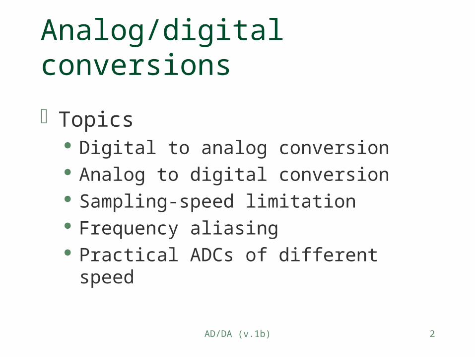
Analog/digital conversions
Topics Digital to analog conversion Analog to digital conversion Sampling-speed limitation Frequency aliasing Practical ADCs of different speed
AD/DA (v.1b) 3
Digital to Analogue Conversion
DAC
AD/DA (v.1b) 4
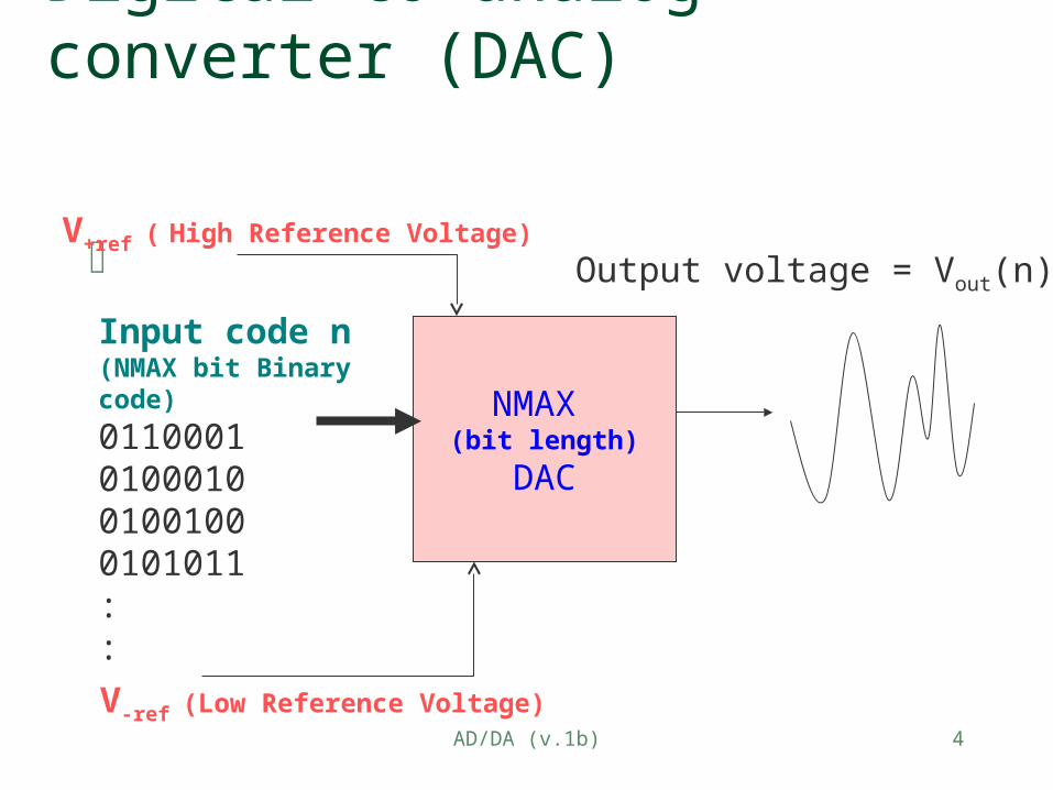
NMAX (bit length)
DAC
Input code n(NMAX bit Binary code)
0110001010001001001000101011::
Output voltage = Vout(n) V+ref ( High Reference Voltage)
V-ref (Low Reference Voltage)
Digital to analog converter (DAC)
AD/DA (v.1b) 5
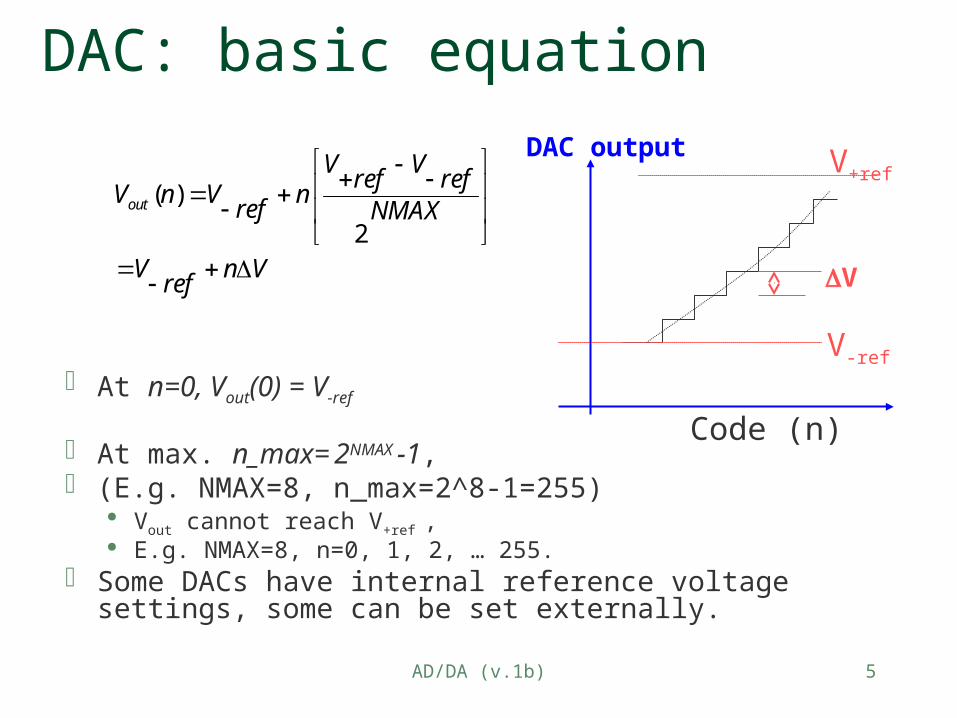
DAC: basic equation
At n=0, Vout(0) = V-ref
At max. n_max= 2NMAX -1, (E.g. NMAX=8, n_max=2^8-1=255)
Vout cannot reach V+ref , E.g. NMAX=8, n=0, 1, 2, … 255.
Some DACs have internal reference voltage settings, some can be set externally.
( )
2out
V Vref ref
V n V nref NMAX
V n Vref
V
V-ref
DAC output V+ref
Code (n)
AD/DA (v.1b) 6
DAC: characteristics
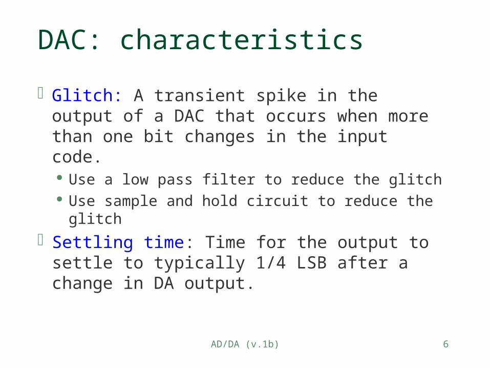
Glitch: A transient spike in the output of a DAC that occurs when more than one bit changes in the input code. Use a low pass filter to reduce the glitch Use sample and hold circuit to reduce the glitch
Settling time: Time for the output to settle to typically 1/4 LSB after a change in DA output.
AD/DA (v.1b) 7
Two DAC implementations
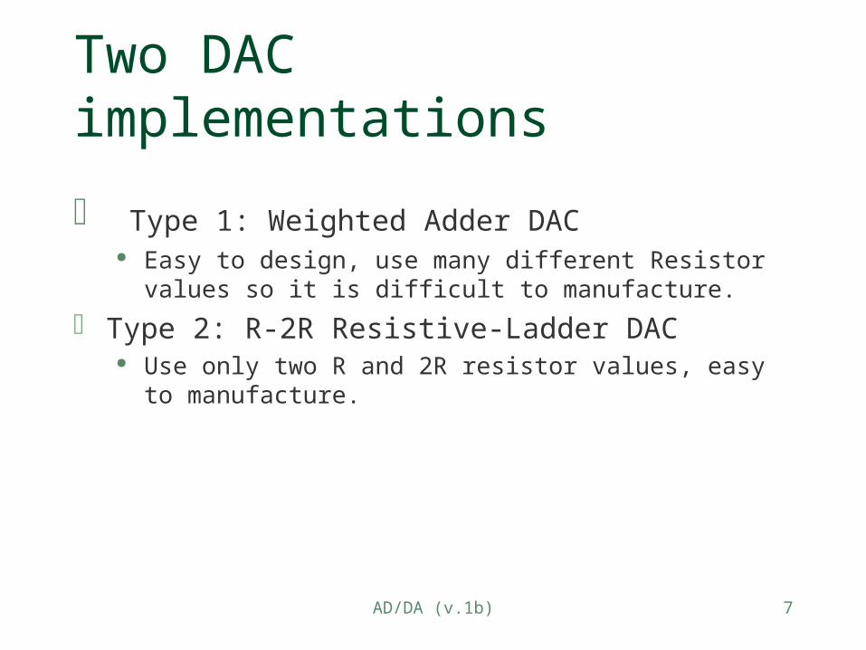
Type 1: Weighted Adder DAC Easy to design, use many different Resistor values so it is difficult
to manufacture.
Type 2: R-2R Resistive-Ladder DAC Use only two R and 2R resistor values, easy to manufacture.
AD/DA (v.1b) 8
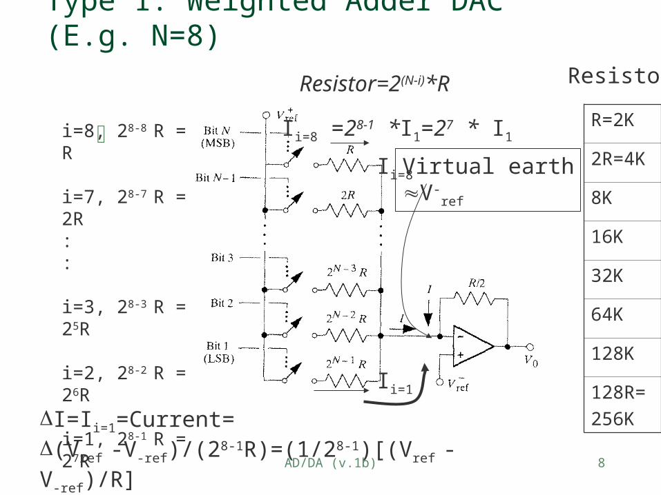
Type 1: Weighted Adder DAC (E.g. N=8)
Virtual earthV-
ref
i=8, 28-8 R = R
i=7, 28-7 R = 2R::
i=3, 28-3 R = 25R
i=2, 28-2 R = 26R
i=1, 28-1 R = 27R
Resistor=2(N-i)*R
Ii=8 =28-1 *I1=27 * I1
I=Ii=1=Current=(Vref -V-ref)/(28-1R)=(1/28-1)[(Vref -V-ref)/R]
Ii=1
Ii=8
R=2K
2R=4K
8K
16K
32K
64K
128K
128R=
256K
Resistor
AD/DA (v.1b) 9
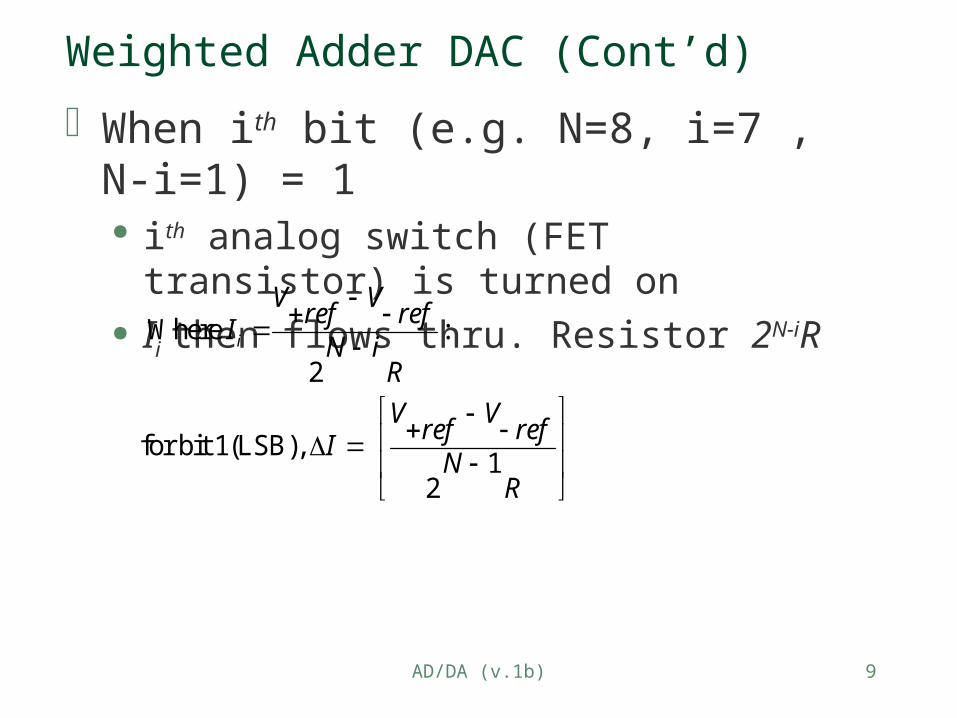
When ith bit (e.g. N=8, i=7 , N-i=1) = 1 ith analog switch (FET transistor) is turned on Ii then flows thru. Resistor 2N-iR
Where :
2
for bit 1(LSB), 1
2
i
V Vref ref
IN i
R
V Vref ref
IN
R
Weighted Adder DAC (Cont’d)
AD/DA (v.1b) 10
When n has only one bit on
0
0
0
For an code n, which has only one bit on
1 / 22
rearrange terms and solving for ,
we have
2
n
V V V Vref ref ref
I n I nN RR
V
V Vref ref
V V nref N
Weighted Adder DAC (Cont’d)
AD/DA (v.1b) 11
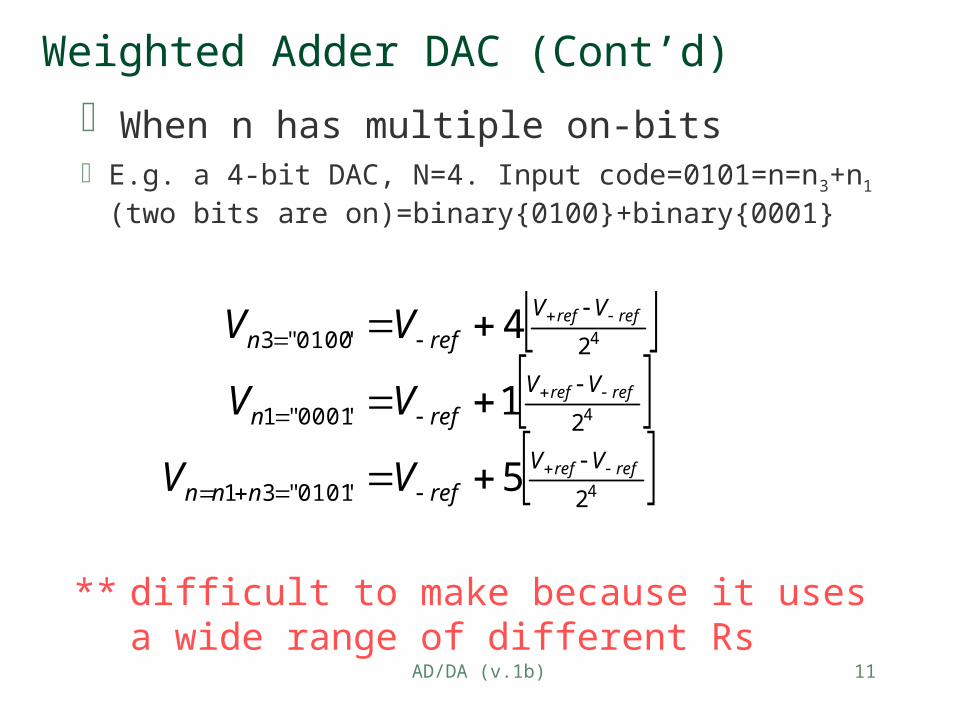
E.g. a 4-bit DAC, N=4. Input code=0101=n=n3+n1 (two bits are on)=binary{0100}+binary{0001}
When n has multiple on-bits
Weighted Adder DAC (Cont’d)
4
4
4
2"0101"31
2"0001"1
2"0100"3
5
1
4
refref
refref
refref
VV
refnnn
VV
refn
VV
refn
VV
VV
VV
** difficult to make because it uses a wide range of different Rs
AD/DA (v.1b) 12
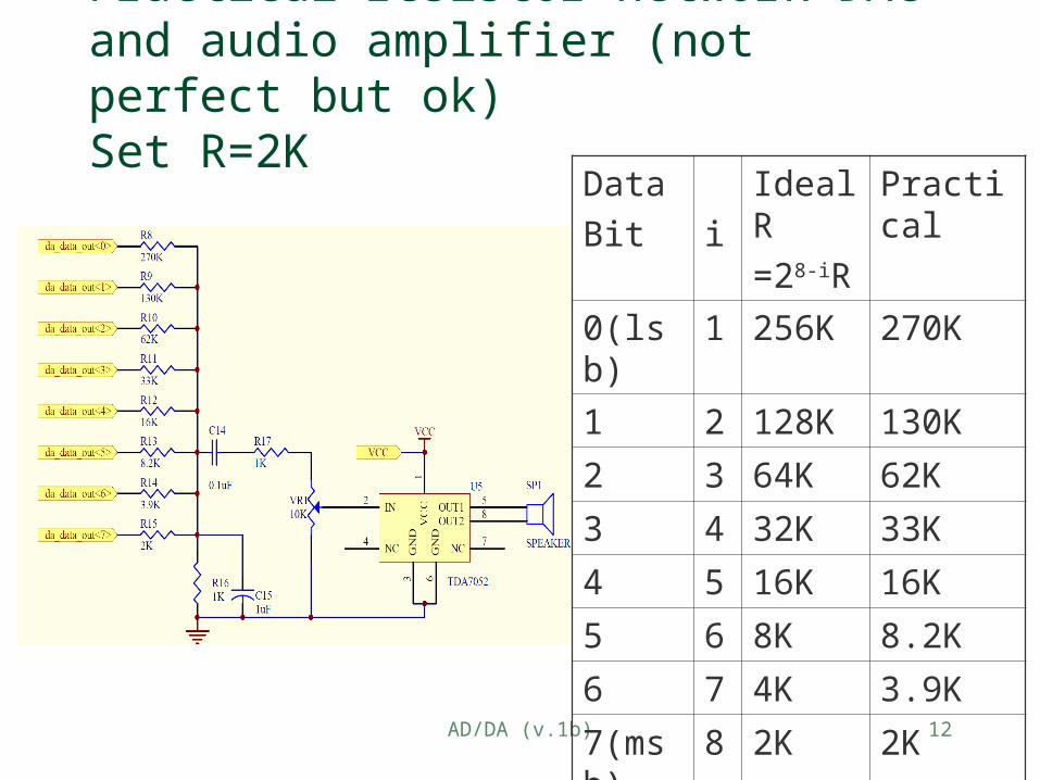
Practical resistor network DAC and audio amplifier (not perfect but ok)Set R=2K
Data
Bit i
Ideal R
=28-iR
Practical
0(lsb) 1 256K 270K
1 2 128K 130K
2 3 64K 62K
3 4 32K 33K
4 5 16K 16K
5 6 8K 8.2K
6 7 4K 3.9K
7(msb) 8 2K 2K
AD/DA (v.1b) 13
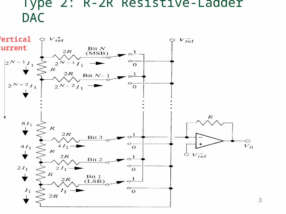
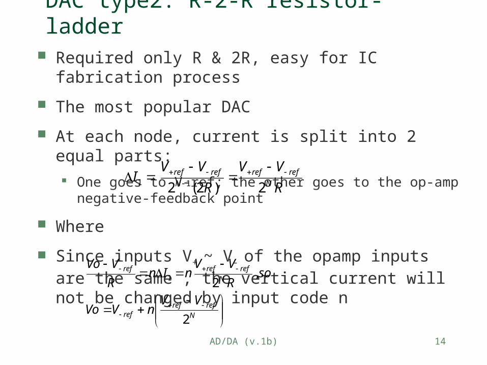
Type 2: R-2R Resistive-Ladder DAC
Vertical current
AD/DA (v.1b) 14
Required only R & 2R, easy for IC fabrication process
The most popular DAC
At each node, current is split into 2 equal parts: One goes to V-ref; the other goes to the op-amp negative-feedback
point
Where
Since inputs V+ ~ V- of the opamp inputs are the same , the vertical current will not be changed by input code n
DAC type2: R-2-R resistor-ladder
R
VV
R
VVI
Nrefref
Nrefref
2)2(2 11
Nrefref
ref
Nrefrefref
VVnVVo
soR
VVnIn
R
VVo
2
,21
AD/DA (v.1b) 15
Analog to Digital Conversion
ADC
AD/DA (v.1b) 16
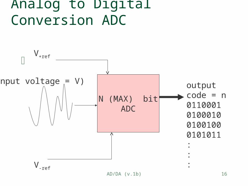
Analog to Digital Conversion ADC
N (MAX) bitADC
output code = n0110001010001001001000101011:::
Input voltage = V)
V+ref
V-ref
AD/DA (v.1b) 17
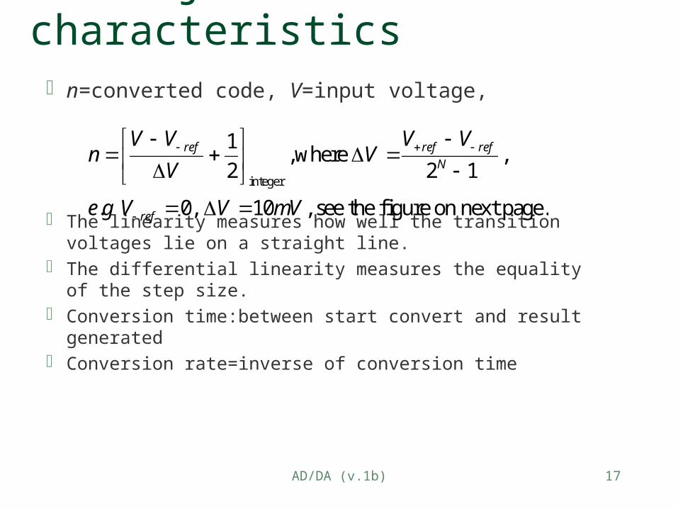
ADC Major characteristicsn=converted code, V=input voltage,
The linearity measures how well the transition voltages lie on a straight line.
The differential linearity measures the equality of the step size. Conversion time:between start convert and result generated Conversion rate=inverse of conversion time
integer
1,where ,
2 2 1
. 0, 10 , see the figure on next page.
ref ref refN
ref
V V V Vn V
V
e g V V mV
AD/DA (v.1b) 18
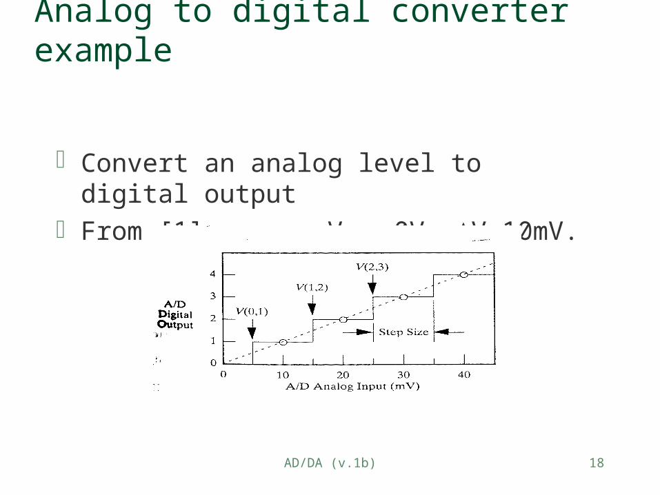
Analog to digital converter example
Convert an analog level to digital outputFrom [1], e.g. V-ref=0V, V=10mV.
AD/DA (v.1b) 19
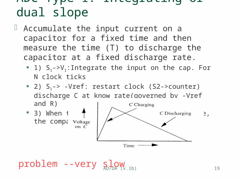
ADC Type 1: Integrating or dual slope Accumulate the input current on a capacitor for a fixed
time and then measure the time (T) to discharge the capacitor at a fixed discharge rate.
1) S1->V1:Integrate the input on the cap. For N clock ticks
2) S1-> -Vref: restart clock (S2->counter) discharge C at know rate(governed by -Vref and R)
3) When the cap. is discharged to 0 voltage, the comparator will stop the counter.
problem --very slow
AD/DA (v.1b) 20
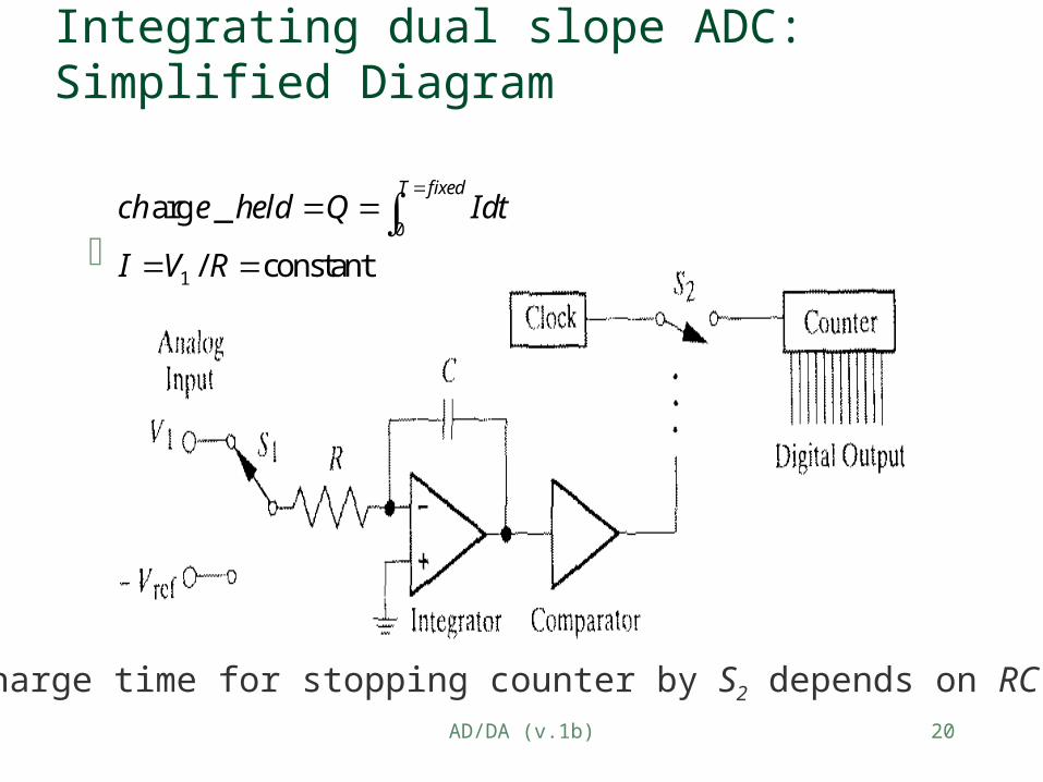
Integrating dual slope ADC: Simplified Diagram
0
1 / tan
T fixedQ Idt
I V R cons t
0
1
arg _
/ constant
T fixedch e held Q Idt
I V R
Discharge time for stopping counter by S2 depends on RC and Q
AD/DA (v.1b) 21
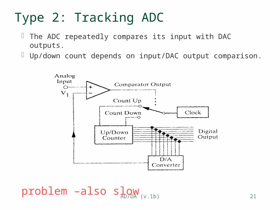
Type 2: Tracking ADC
The ADC repeatedly compares its input with DAC outputs. Up/down count depends on input/DAC output comparison.
problem –also slow
AD/DA (v.1b) 22
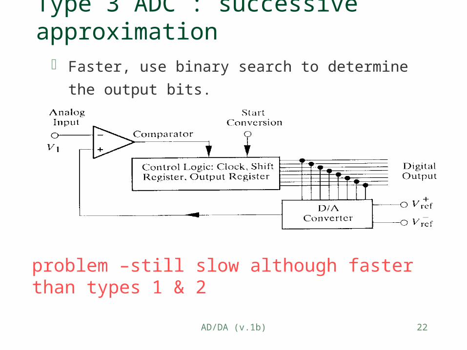
Type 3 ADC : successive approximation
Faster, use binary search to determine the output bits.
problem –still slow although faster than types 1 & 2
AD/DA (v.1b) 23
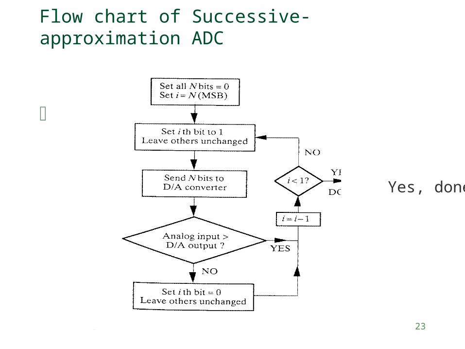
Flow chart of Successive-approximation ADC
Yes, done
AD/DA (v.1b) 24
Type 4 ADC : Flash ADC (very fast)
Divide the voltage range into 2N-1 levels; use 2N-1 comparators to determine what the voltage level is
Use a 2N-1 input to N bit priority decoder to work out the binary number
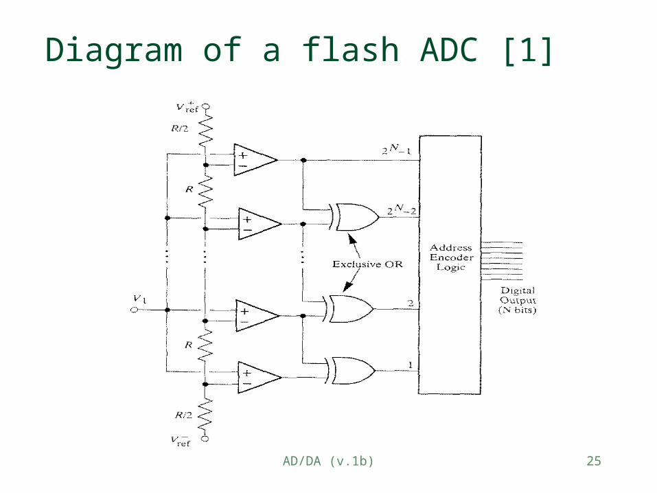
AD/DA (v.1b) 25
Diagram of a flash ADC [1]
AD/DA (v.1b) 26
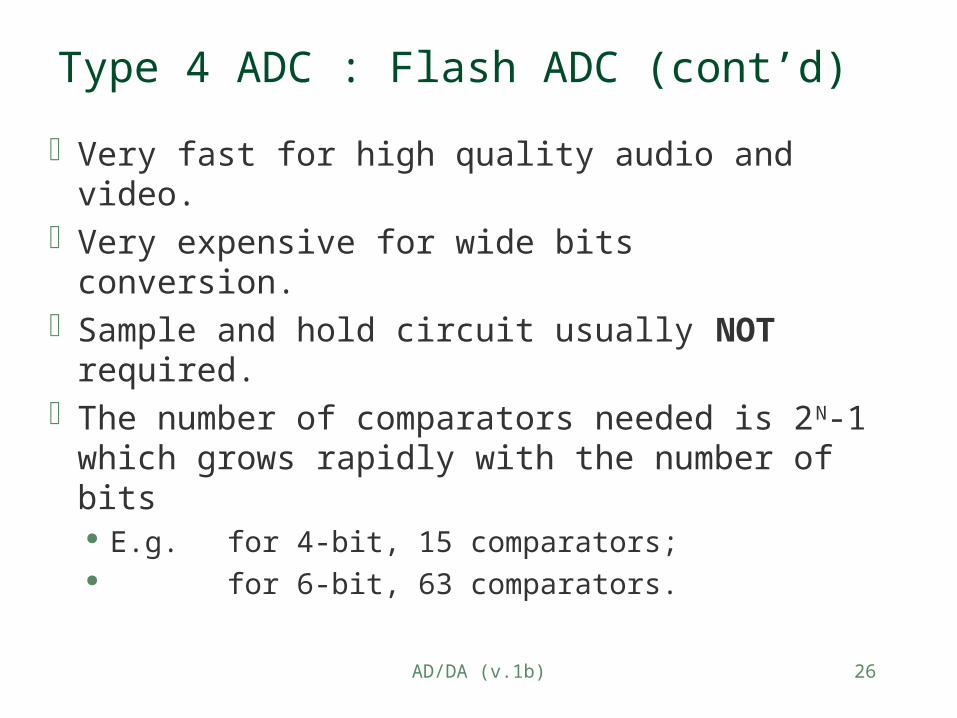
Type 4 ADC : Flash ADC (cont’d)
Very fast for high quality audio and video.Very expensive for wide bits conversion.Sample and hold circuit usually NOT
required.The number of comparators needed is 2N-1
which grows rapidly with the number of bits E.g. for 4-bit, 15 comparators; for 6-bit, 63 comparators.
AD/DA (v.1b) 27
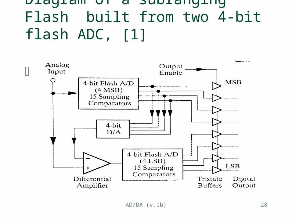
Type 5 ADC : subranging Flash ADC
Compromise; medium speed Pure Flash ADC is very expensive for large number
of bits.Subranging Flash ADC is Hybrid between successive
approximation and flash.AD7280 or ADC0820 uses two 4-bit flash ADC to
build an 8-bit subranging Flash ADC.Figure next page: Upper 4-bit (MSB) flash ADC
finds coarse MSB digital output, then converts into approximate analog level by a 4-bit DAC, the lower 4-bit flash ADC finds the fine 4-bit (LSB) digital code.
AD/DA (v.1b) 28
Diagram of a subranging Flash built from two 4-bit flash ADC, [1]
AD/DA (v.1b) 29
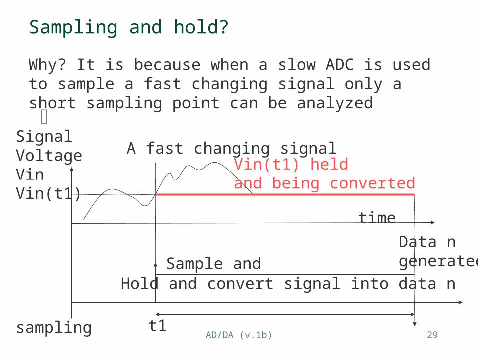
Sampling and hold?
SignalVoltageVinVin(t1)
sampling
Sample andHold and convert signal into data n
Data ngenerated
t1
Vin(t1) heldand being converted
time
A fast changing signal
Why? It is because when a slow ADC is used to sample a fast changing signal only a short sampling point can be analyzed
AD/DA (v.1b) 30
Sampling-speed limitation
Given the conversion time of an ADC is Tconv seconds, the maximum sampling rate is Fmax=1/T (Hz) .
E.g: ADC0801, Tconv =114ns+P to ADC delay,
Fmax < 8.77KHz
For this sample rate the maximum frequency for the input is (Fmax/2) < 4.39KHz by Nyquist sampling theory.
Need to use a sample-and-hold circuit to freeze a fast changing input when using a low speed ADC to convert the signal.
For high speed conversion, use Direct-Memory-Access (DMA) to copy the data directly to P memory to reduce P to ADC delay.
AD/DA (v.1b) 31
Frequency aliasing
When the highest frequency of the signal Finput is greater than half the sampling ( Fsampling/2).
E.g. Finput =20KHz,
Fsampling must be over 40KHz.
Remedy: Use a low pass filter to cut off the input high frequency content before ADC sampling.
AD/DA (v.1b) 32
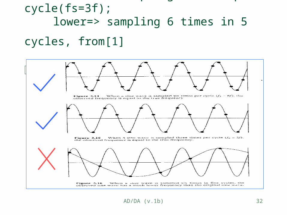
upper => sampling 6 times per cycle(fs=6f); middle => sampling 3 times per cycle(fs=3f);
lower=> sampling 6 times in 5 cycles, from[1]
AD/DA (v.1b) 33
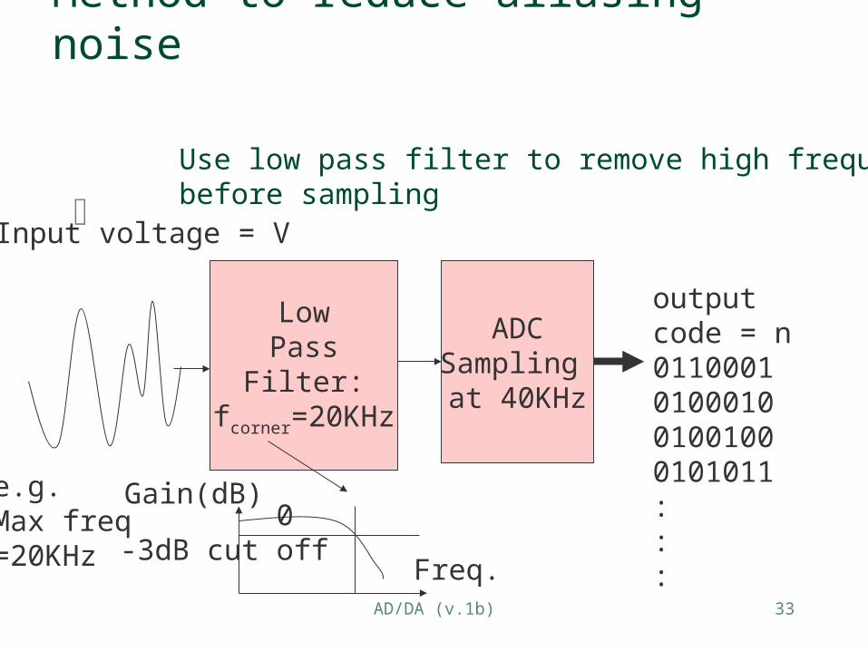
Method to reduce aliasing noise
ADCSampling at 40KHz
output code = n0110001010001001001000101011:::
Input voltage = V
LowPass
Filter:fcorner=20KHz
e.g. Max freq=20KHz
Use low pass filter to remove high frequency before sampling
Freq.
Gain(dB) 0-3dB cut off
AD/DA (v.1b) 34
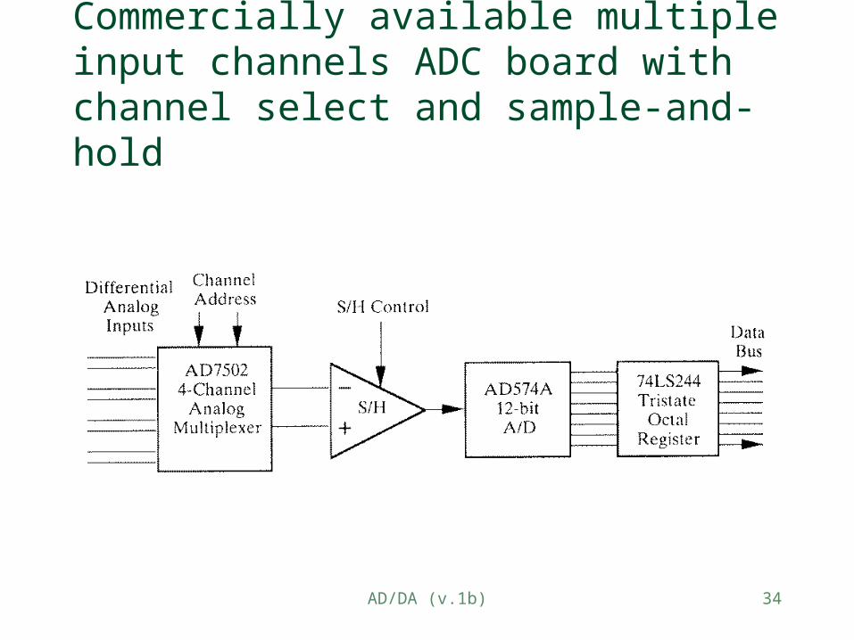
Commercially available multiple input channels ADC board with channel select and sample-and-hold
AD/DA (v.1b) 35
Practical ADCs
Low cost, low speed (successive approximation, 8bit-8KHz sampling), National semiconductor ADC0801,2,3,4 family. See http://www.national.com/catalog/
Medium speed (half-flash, 8-bit 666KHz), National semiconductor ADC0820.
High speed (flash 8-bit,4080MHz, video quality) Philips TDA8714 (/7/6/4) family. See http://207.87.19.21/products/
AD/DA (v.1b) 36
ADC0801 description from http://www.national.com/catalog/ 8-bit successive approximation A/D converters that use a
differential potentiometric ladder-similar to the 256R products.
Output latches directly driving the data bus. These A/Ds appear like memory locations or I/O ports to the
microprocessor and no interfacing logic is needed. Differential analog voltage inputs allow increasing the
common-mode rejection and offsetting the analog zero input voltage value.
Voltage reference input can be adjusted to allow encoding any smaller analog voltage span to the full 8 bits of resolution.
AD/DA (v.1b) 37
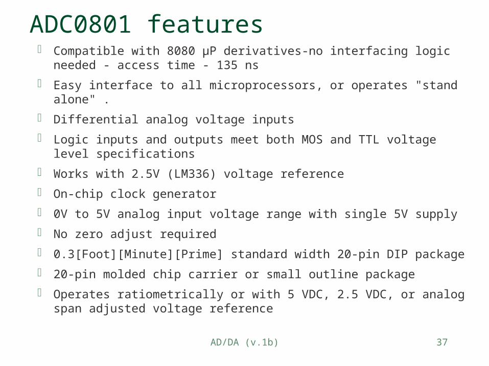
ADC0801 features Compatible with 8080 µP derivatives-no interfacing logic needed - access
time - 135 ns
Easy interface to all microprocessors, or operates "stand alone" .
Differential analog voltage inputs
Logic inputs and outputs meet both MOS and TTL voltage level specifications
Works with 2.5V (LM336) voltage reference
On-chip clock generator
0V to 5V analog input voltage range with single 5V supply
No zero adjust required
0.3[Foot][Minute][Prime] standard width 20-pin DIP package
20-pin molded chip carrier or small outline package
Operates ratiometrically or with 5 VDC, 2.5 VDC, or analog span adjusted voltage reference
AD/DA (v.1b) 38
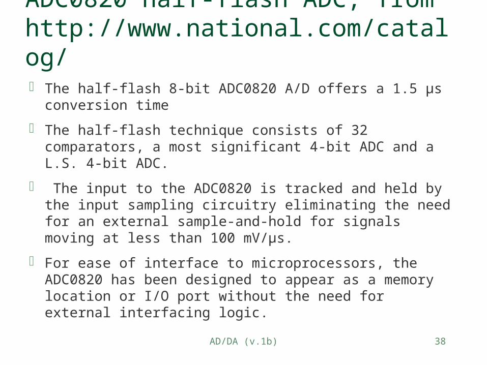
ADC0820 half-flash ADC, from http://www.national.com/catalog/ The half-flash 8-bit ADC0820 A/D offers a 1.5 µs conversion
time
The half-flash technique consists of 32 comparators, a most significant 4-bit ADC and a L.S. 4-bit ADC.
The input to the ADC0820 is tracked and held by the input sampling circuitry eliminating the need for an external sample-and-hold for signals moving at less than 100 mV/µs.
For ease of interface to microprocessors, the ADC0820 has been designed to appear as a memory location or I/O port without the need for external interfacing logic.
AD/DA (v.1b) 39
ADC0820 features
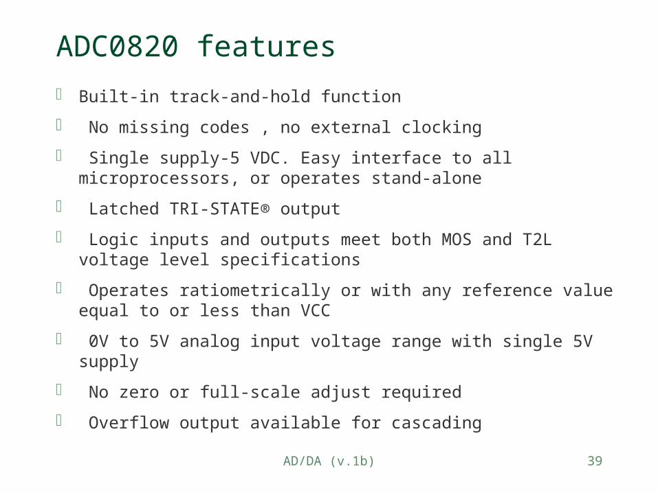
Built-in track-and-hold function
No missing codes , no external clocking
Single supply-5 VDC. Easy interface to all microprocessors, or operates stand-alone
Latched TRI-STATE® output
Logic inputs and outputs meet both MOS and T2L voltage level specifications
Operates ratiometrically or with any reference value equal to or less than VCC
0V to 5V analog input voltage range with single 5V supply
No zero or full-scale adjust required
Overflow output available for cascading
AD/DA (v.1b) 40
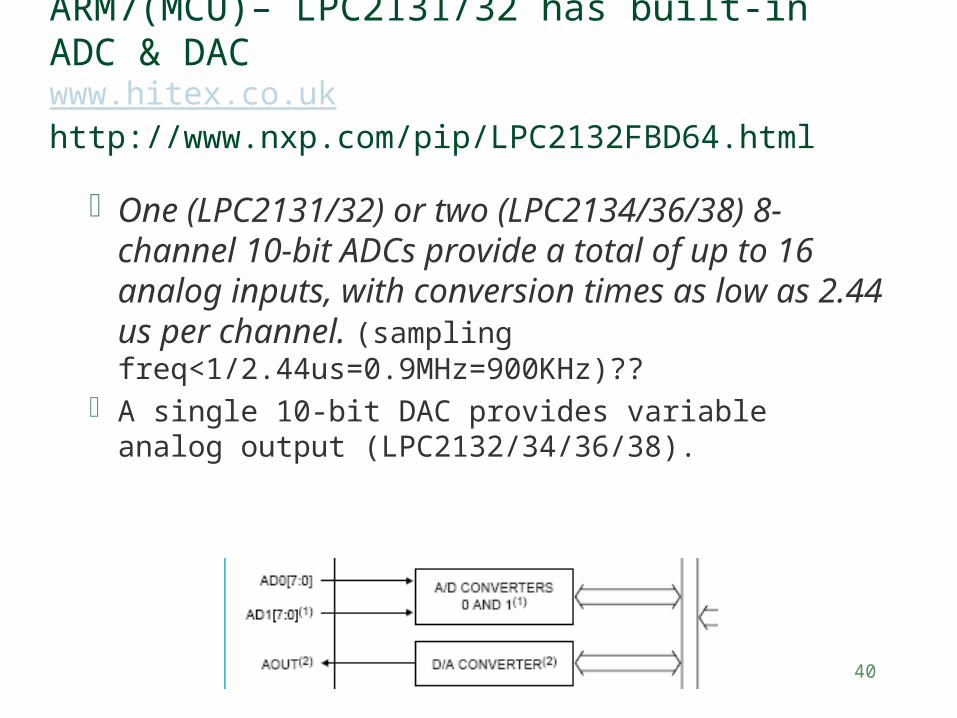
ARM7(MCU)– LPC2131/32 has built-in ADC & DACwww.hitex.co.ukhttp://www.nxp.com/pip/LPC2132FBD64.html
One (LPC2131/32) or two (LPC2134/36/38) 8-channel 10-bit ADCs provide a total of up to 16 analog inputs, with conversion times as low as 2.44 us per channel. (sampling freq<1/2.44us=0.9MHz=900KHz)??
A single 10-bit DAC provides variable analog output (LPC2132/34/36/38).
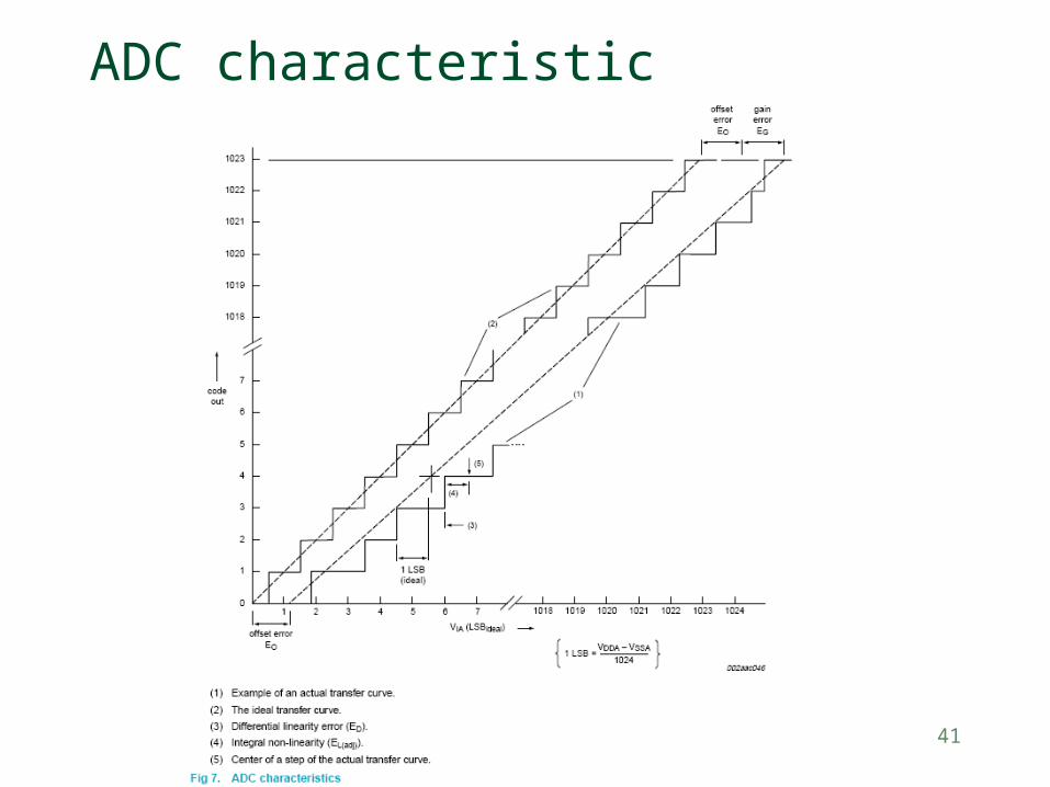
AD/DA (v.1b) 41
ADC characteristic
AD/DA (v.1b) 42
Summary
Studied the operations of Digital/analogue conversions.
Studied the application of Digital/analogue converters.
AD/DA (v.1b) 43
References
[1] Interfacing: A Laboratory Approach Using the Microcomputer for Instrumentation, Data Analysis, and Control by Stephen E. Derenzo
[2] http://www.nxp.com/pip/LPC2132FBD64.html
Related Documents