TPS54329DDA V (50 mV/div) OUT I (1 A/div) OUT 100 s/div μ G006 TPS54329 www.ti.com SLVSAZ6A – SEPTEMBER 2011 – REVISED MARCH 2012 4.5V to 18V Input, 3-A SYNCHRONOUS STEP DOWN CONVERTER Check for Samples: TPS54329 1FEATURES DESCRIPTION The TPS54329 is an adaptive on-time D-CAP2™ 23• D-CAP2™ Mode Enables Fast Transient mode synchronous buck converter. TheTPS54329 Response enables system designers to complete the suite of • Low Output Ripple and Allows Ceramic Output various end equipment’s power bus regulators with a Capacitor cost effective, low component count, low standby current solution. The main control loop for the • Wide V IN Input Voltage Range: 4.5 V to 18 V TPS54329 uses the D-CAP2™ mode control which • Output Voltage Range: 0.76 V to 7.0 V provides a fast transient response with no external • Highly Efficient Integrated FETs Optimized compensation components. The TPS54329 also has for Lower Duty Cycle Applications a proprietary circuit that enables the device to adopt – 100 mΩ (High Side) and 74 mΩ (Low Side) to both low equivalent series resistance (ESR) output capacitors, such as POSCAP or SP-CAP, and ultra- • High Efficiency, Less Than 10 μA at Shutdown low ESR ceramic capacitors. The device operates • High Initial Bandgap Reference Accuracy from 4.5-V to 18-V VIN input. The output voltage can • Adjustable Soft Start be programmed between 0.76 V and 7 V. The device also features an adjustable soft start time. The • Pre-Biased Soft Start TPS54329 is available in the 8-pin DDA package, • 650-kHz Switching Frequency (f SW ) and designed to operate from –40°C to 85°C. • Cycle By Cycle Over Current Limit APPLICATIONS • Wide Range of Applications for Low Voltage System – Digital TV Power Supply – High Definition Blu-ray Disc™ Players – Networking Home Terminal – Digital Set Top Box (STB) 1 Please be aware that an important notice concerning availability, standard warranty, and use in critical applications of Texas Instruments semiconductor products and disclaimers thereto appears at the end of this data sheet. 2D-CAP2 is a trademark of Texas Instruments. 3Blu-ray Disc is a trademark of Blu-ray Disc Association. PRODUCTION DATA information is current as of publication date. Copyright © 2011–2012, Texas Instruments Incorporated Products conform to specifications per the terms of the Texas Instruments standard warranty. Production processing does not necessarily include testing of all parameters.

Welcome message from author
This document is posted to help you gain knowledge. Please leave a comment to let me know what you think about it! Share it to your friends and learn new things together.
Transcript
TPS54329DDA
V (50 mV/div)OUT
I (1 A/div)OUT
100 s/divμ
G006
TPS54329
www.ti.com SLVSAZ6A –SEPTEMBER 2011–REVISED MARCH 2012
4.5V to 18V Input, 3-A SYNCHRONOUS STEP DOWN CONVERTERCheck for Samples: TPS54329
1FEATURES DESCRIPTIONThe TPS54329 is an adaptive on-time D-CAP2™
23• D-CAP2™ Mode Enables Fast Transientmode synchronous buck converter. TheTPS54329Responseenables system designers to complete the suite of
• Low Output Ripple and Allows Ceramic Output various end equipment’s power bus regulators with aCapacitor cost effective, low component count, low standby
current solution. The main control loop for the• Wide VIN Input Voltage Range: 4.5 V to 18 VTPS54329 uses the D-CAP2™ mode control which• Output Voltage Range: 0.76 V to 7.0 Vprovides a fast transient response with no external
• Highly Efficient Integrated FETs Optimized compensation components. The TPS54329 also hasfor Lower Duty Cycle Applications a proprietary circuit that enables the device to adopt– 100 mΩ (High Side) and 74 mΩ (Low Side) to both low equivalent series resistance (ESR) output
capacitors, such as POSCAP or SP-CAP, and ultra-• High Efficiency, Less Than 10 μA at Shutdownlow ESR ceramic capacitors. The device operates• High Initial Bandgap Reference Accuracyfrom 4.5-V to 18-V VIN input. The output voltage can
• Adjustable Soft Start be programmed between 0.76 V and 7 V. The devicealso features an adjustable soft start time. The• Pre-Biased Soft StartTPS54329 is available in the 8-pin DDA package,• 650-kHz Switching Frequency (fSW)and designed to operate from –40°C to 85°C.
• Cycle By Cycle Over Current Limit
APPLICATIONS• Wide Range of Applications for Low Voltage
System– Digital TV Power Supply– High Definition Blu-ray Disc™ Players– Networking Home Terminal– Digital Set Top Box (STB)
1
Please be aware that an important notice concerning availability, standard warranty, and use in critical applications ofTexas Instruments semiconductor products and disclaimers thereto appears at the end of this data sheet.
2D-CAP2 is a trademark of Texas Instruments.3Blu-ray Disc is a trademark of Blu-ray Disc Association.
PRODUCTION DATA information is current as of publication date. Copyright © 2011–2012, Texas Instruments IncorporatedProducts conform to specifications per the terms of the TexasInstruments standard warranty. Production processing does notnecessarily include testing of all parameters.
TPS54329
SLVSAZ6A –SEPTEMBER 2011–REVISED MARCH 2012 www.ti.com
This integrated circuit can be damaged by ESD. Texas Instruments recommends that all integrated circuits be handled withappropriate precautions. Failure to observe proper handling and installation procedures can cause damage.
ESD damage can range from subtle performance degradation to complete device failure. Precision integrated circuits may be moresusceptible to damage because very small parametric changes could cause the device not to meet its published specifications.
ORDERING INFORMATION (1)
TRANSPORTTA PACKAGE (2) (3) ORDERABLE PART NUMBER PIN MEDIA
TPS54329DDA Tube–40°C to 85°C DDA 8
TPS54329DDAR Tape and Reel
(1) For the most current package and ordering information, see the Package Option Addendum at the end of this document, or see the TIweb site at www.ti.com.
(2) Package drawings, thermal data, and symbolization are available at www.ti.com/packaging.(3) All package options have Cu NIPDAU lead/ball finish.
ABSOLUTE MAXIMUM RATINGSover operating free-air temperature range (unless otherwise noted) (1)
VALUEUNIT
MIN MAX
VIN, EN –0.3 20 V
VBST –0.3 26 V
VBST (10 ns transient) –0.3 28 V
Input voltage range VBST (vs SW) –0.3 6.5 V
VFB, SS –0.3 6.5 V
SW –2 20 V
SW (10 ns transient) –3 22 V
VREG5 –0.3 6.5 VOutput voltage range
GND –0.3 0.3 V
Voltage from GND to thermal pad, Vdiff –0.2 0.2 V
Human Body Model (HBM) 2 kVElectrostatic discharge
Charged Device Model (CDM) 500 V
Operating junction temperature, TJ –40 150 °C
Storage temperature, Tstg –55 150 °C
(1) Stresses beyond those listed under absolute maximum ratings may cause permanent damage to the device. These are stress ratingsonly, and functional operation of the device at these or any other conditions beyond those indicated under recommended operatingconditions is not implied. Exposure to absolute-maximum-rated conditions for extended periods may affect device reliability.
THERMAL INFORMATIONTPS54329
THERMAL METRIC UNITSDDA (8 PINS)
θJA Junction-to-ambient thermal resistance 42.1
θJCtop Junction-to-case (top) thermal resistance 50.9
θJB Junction-to-board thermal resistance 31.8°C/W
ψJT Junction-to-top characterization parameter 5
ψJB Junction-to-board characterization parameter 13.5
θJCbot Junction-to-case (bottom) thermal resistance 7.1
2 Copyright © 2011–2012, Texas Instruments Incorporated
Product Folder Link(s): TPS54329
TPS54329
www.ti.com SLVSAZ6A –SEPTEMBER 2011–REVISED MARCH 2012
RECOMMENDED OPERATING CONDITIONSover operating free-air temperature range (unless otherwise noted)
MIN MAX UNIT
VIN Supply input voltage range 4.5 18 V
VBST –0.1 24
VBST (10 ns transient) -0.1 27
VBST(vs SW) –0.1 5.7
SS –0.1 5.7
VI Input voltage range EN –0.1 18 V
VFB –0.1 5.5
SW –1.8 18
SW (10 ns transient) –3 21
GND –0.1 0.1
VO Output voltage range VREG5 –0.1 5.7 V
IO Output Current range IVREG5 0 10 mA
TA Operating free-air temperature –40 85 °C
TJ Operating junction temperature –40 150 °C
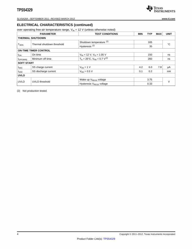
ELECTRICAL CHARACTERISTICSover operating free-air temperature range, VIN = 12 V (unless otherwise noted)
PARAMETER TEST CONDITIONS MIN TYP MAX UNIT
SUPPLY CURRENT
VIN current, TA = 25°C, EN = 5 V,IVIN Operating - non-switching supply current 800 1200 μAVFB = 0.8 V
IVINSDN Shutdown supply current VIN current, TA = 25°C, EN = 0 V 4.3 10 μA
LOGIC THRESHOLD
VENH EN high-level input voltage EN 1.6 V
VENL EN low-level input voltage EN 0.45 V
REN EN pin resistance to GND VEN = 12 V 220 440 880 kΩVFB VOLTAGE AND DISCHARGE RESISTANCE
VFBTH VFB threshold voltage TA = 25°C, VO = 1.05 V, continuous mode 749 765 781 mV
IVFB VFB input current VFB = 0.8 V, TA = 25°C 0 ±0.1 μA
VREG5 OUTPUT
TA = 25°C, 6.0 V < VIN < 18 V,VVREG5 VREG5 output voltage 5.5 V0 < IVREG5 < 5 mA
IVREG5 Output current VIN = 6 V, VREG5 = 4.0 V, TA = 25°C (1) 60 mA
MOSFET
RDS(on)h High side switch resistance 25°C, VBST - SW = 5.5 V (1) 100 mΩRDS(on)l Low side switch resistance 25°C (1) 74 mΩCURRENT LIMIT
Iocl Current limit L out = 1.5 μH (1) 3.5 4.2 5.7 A
(1) Not production tested.
Copyright © 2011–2012, Texas Instruments Incorporated 3
Product Folder Link(s): TPS54329
TPS54329
SLVSAZ6A –SEPTEMBER 2011–REVISED MARCH 2012 www.ti.com
ELECTRICAL CHARACTERISTICS (continued)over operating free-air temperature range, VIN = 12 V (unless otherwise noted)
PARAMETER TEST CONDITIONS MIN TYP MAX UNIT
THERMAL SHUTDOWN
Shutdown temperature (2) 165TSDN Thermal shutdown threshold °C
Hysteresis (2) 35
ON-TIME TIMER CONTROL
tON On time VIN = 12 V, VO = 1.05 V 150 ns
tOFF(MIN) Minimum off time TA = 25°C, VFB = 0.7 V (2) 260 ns
SOFT START
ISSC SS charge current VSS = 1 V 4.2 6.0 7.8 μA
ISSD SS discharge current VSS = 0.5 V 0.1 0.2 mA
UVLO
Wake up VREG5 voltage 3.75UVLO UVLO threshold V
Hysteresis VREG5 voltage 0.33
(2) Not production tested.
4 Copyright © 2011–2012, Texas Instruments Incorporated
Product Folder Link(s): TPS54329
TPS54329
DDA
(HSOP8)
Power PAD
1
2
3
4 5
6
7
8
SW
GND
VBST
VIN EN
VFB
VREG5
SS
TPS54329
www.ti.com SLVSAZ6A –SEPTEMBER 2011–REVISED MARCH 2012
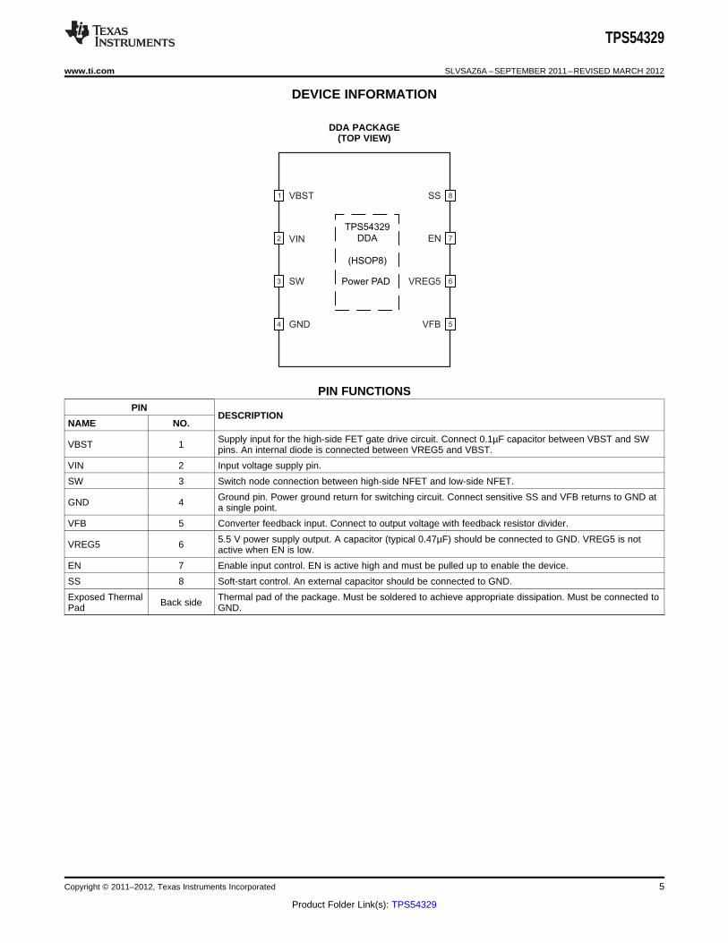
DEVICE INFORMATION
DDA PACKAGE(TOP VIEW)
PIN FUNCTIONSPIN
DESCRIPTIONNAME NO.
Supply input for the high-side FET gate drive circuit. Connect 0.1µF capacitor between VBST and SWVBST 1 pins. An internal diode is connected between VREG5 and VBST.
VIN 2 Input voltage supply pin.
SW 3 Switch node connection between high-side NFET and low-side NFET.
Ground pin. Power ground return for switching circuit. Connect sensitive SS and VFB returns to GND atGND 4 a single point.
VFB 5 Converter feedback input. Connect to output voltage with feedback resistor divider.
5.5 V power supply output. A capacitor (typical 0.47µF) should be connected to GND. VREG5 is notVREG5 6 active when EN is low.
EN 7 Enable input control. EN is active high and must be pulled up to enable the device.
SS 8 Soft-start control. An external capacitor should be connected to GND.
Exposed Thermal Thermal pad of the package. Must be soldered to achieve appropriate dissipation. Must be connected toBack sidePad GND.
Copyright © 2011–2012, Texas Instruments Incorporated 5
Product Folder Link(s): TPS54329
SW
VBST
EN
VFB
GND
VO
4
3
1
VIN
SS
VIN
VREG5
EN
Logic
SW
PGND
Protection
Logic
Ref
SS
UVLO
UVLO
SoftstartSS
REF
TSD
Ref
VREG5
2
VIN
CeramicCapacitor6
SGND
SGND
PGND
PWM+
-
+
OCP
+
-
VREG5
XCON
VREG5
Control Logic
1 shot
ON
5
7
8
TPS54329
SLVSAZ6A –SEPTEMBER 2011–REVISED MARCH 2012 www.ti.com
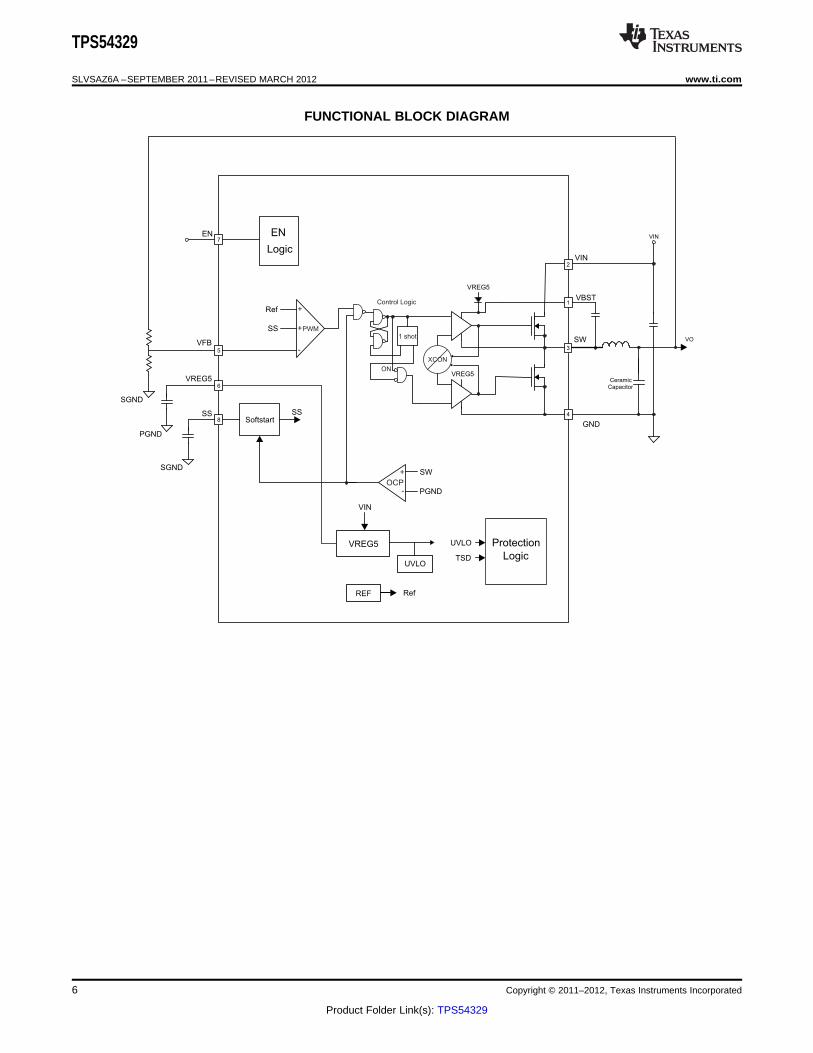
FUNCTIONAL BLOCK DIAGRAM
6 Copyright © 2011–2012, Texas Instruments Incorporated
Product Folder Link(s): TPS54329
(nF) x V (nF) x 0.765 1.1REFSS SSt (ms) = =
SS I ( A)SS
C 1.1 C
6
´
m
´
TPS54329
www.ti.com SLVSAZ6A –SEPTEMBER 2011–REVISED MARCH 2012
OVERVIEW
The TPS54329 is a 3-A synchronous step-down (buck) converter with two integrated N-channel MOSFETs. Itoperates using D-CAP2™ mode control. The fast transient response of D-CAP2™ control reduces the outputcapacitance required to meet a specific level of performance. Proprietary internal circuitry allows the use of lowESR output capacitors including ceramic and special polymer types.
DETAILED DESCRIPTION
PWM Operation
The main control loop of the TPS54329 is an adaptive on-time pulse width modulation (PWM) controller thatsupports a proprietary D-CAP2™ mode control. D-CAP2™ mode control combines constant on-time control withan internal compensation circuit for pseudo-fixed frequency and low external component count configuration withboth low ESR and ceramic output capacitors. It is stable even with virtually no ripple at the output.
At the beginning of each cycle, the high-side MOSFET is turned on. This MOSFET is turned off after internal oneshot timer expires. This one shot is set by the converter input voltage, VIN, and the output voltage, VO, tomaintain a pseudo-fixed frequency over the input voltage range, hence it is called adaptive on-time control. Theone-shot timer is reset and the high-side MOSFET is turned on again when the feedback voltage falls below thereference voltage. An internal ramp is added to reference voltage to simulate output ripple, eliminating the needfor ESR induced output ripple from D-CAP2™ mode control.
PWM Frequency and Adaptive On-Time Control
TPS54329 uses an adaptive on-time control scheme and does not have a dedicated on board oscillator. TheTPS54329 runs with a pseudo-constant frequency of 650 kHz by using the input voltage and output voltage toset the on-time one-shot timer. The on-time is inversely proportional to the input voltage and proportional to theoutput voltage, therefore, when the duty ratio is VOUT/VIN, the frequency is constant.
Soft Start and Pre-Biased Soft Start
The soft start function is adjustable. When the EN pin becomes high, 6 μA current begins charging the capacitorwhich is connected from the SS pin to GND. Smooth control of the output voltage is maintained during start up.The equation for the slow start time is shown in Equation 1. VFB voltage is 0.765 V and SS pin source current is6 μA.
(1)
The TPS54329 contains a unique circuit to prevent current from being pulled from the output during startup if theoutput is pre-biased. When the soft-start commands a voltage higher than the pre-bias level (internal soft startbecomes greater than feedback voltage VFB), the controller slowly activates synchronous rectification by startingthe first low side FET gate driver pulses with a narrow on-time. It then increments that on-time on a cycle-by-cycle basis until it coincides with the time dictated by (1-D), where D is the duty cycle of the converter. Thisscheme prevents the initial sinking of the pre-bias output, and ensure that the out voltage (VO) starts and rampsup smoothly into regulation and the control loop is given time to transition from pre-biased start-up to normalmode operation.
Current Protection
The output overcurrent protection (OCP) is implemented using a cycle-by-cycle valley detect control circuit. Theswitch current is monitored by measuring the low-side FET switch voltage between the SW pin and GND. Thisvoltage is proportional to the switch current. To improve accuracy, the voltage sensing is temperaturecompensated.
During the on time of the high-side FET switch, the switch current increases at a linear rate determined by Vin,Vout, the on-time and the output inductor value. During the on time of the low-side FET switch, this currentdecreases linearly. The average value of the switch current is the load current IOUT. The TPS54329 constantlymonitors the low-side FET switch voltage, which is proportional to the switch current, during the low-side on-time.If the measured voltage is above the voltage proportional to the current limit, an internal counter is incrementedper each SW cycle and the converter maintains the low-side switch on until the measured voltage is below thevoltage corresponding to the current limit at which time the switching cycle is terminated and a new switching
Copyright © 2011–2012, Texas Instruments Incorporated 7
Product Folder Link(s): TPS54329
TPS54329
SLVSAZ6A –SEPTEMBER 2011–REVISED MARCH 2012 www.ti.com
cycle begins. In subsequent switching cycles, the on-time is set to a fixed value and the current is monitored inthe same manner. If the over current condition exists for 7 consecutive switching cycles, the internal OCLthreshold is set to a lower level, reducing the available output current. When a switching cycle occurs where theswitch current is not above the lower OCL threshold, the counter is reset and the OCL limit is returned to thehigher value.
There are some important considerations for this type of over-current protection. The load current one half of thepeak-to-peak inductor current higher than the over-current threshold. Also when the current is being limited, theoutput voltage tends to fall as the demanded load current may be higher than the current available from theconverter. This may cause the output voltage to fall. When the over current condition is removed, the outputvoltage will return to the regulated value. This protection is non-latching.
UVLO Protection
Undervoltage lock out protection (UVLO) monitors the voltage of the VREG5 pin. When the VREG5 voltage is lowerthan UVLO threshold voltage, the TPS54329 is shut off. This is protection is non-latching.
Thermal Shutdown
TPS54329 monitors the temperature of itself. If the temperature exceeds the threshold value (typically 165°C),the device is shut off. This is non-latch protection.
8 Copyright © 2011–2012, Texas Instruments Incorporated
Product Folder Link(s): TPS54329
0
200
400
600
800
1000
1200
−50 0 50 100 150Junction Temperature (°C)
Sup
ply
Cur
rent
(µA
)
VIN = 12 V
G001
0
2
4
6
8
10
12
14
16
−50 0 50 100 150Junction Temperature (°C)
Shu
tdow
n C
urre
nt (
µA)
VIN = 12 V
G002
0
5
10
15
20
25
30
35
40
45
50
0 5 10 15 20EN Input Voltage (V)
EN
Inpu
t Cur
rent
(µA
)
VIN = 18 V
G003
1.03
1.04
1.05
1.06
1.07
0.0 0.5 1.0 1.5 2.0 2.5 3.0Output Current (A)
Out
put V
olta
ge (
V)
VIN = 5 VVIN = 12 VVIN = 18 V
L = CLF7045
G004
V (50 mV/div)OUT
I (1 A/div)OUT
100 s/divμ
G006
1.03
1.04
1.05
1.06
1.07
0 5 10 15 20Input Voltage (V)
Out
put V
olta
ge (
V)
IOUT = 0 AIOUT = 1 A
G005
TPS54329
www.ti.com SLVSAZ6A –SEPTEMBER 2011–REVISED MARCH 2012
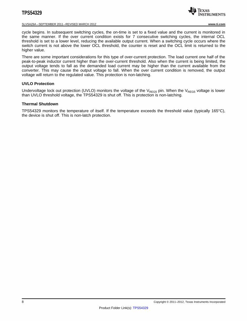
TYPICAL CHARACTERISTICSVIN = 12 V, TA = 25°C (unless otherwise noted).
Figure 1. VIN CURRENT vs JUNCTION TEMPERATURE Figure 2. VIN SHUTDOWN CURRENT vsJUNCTION TEMPERATURE
Figure 3. EN CURRENT vs EN VOLTAGE Figure 4. 1.05-V OUTPUT VOLTAGE vs OUTPUT CURRENT
Figure 5. 1.05-V OUTPUT VOLTAGE vs INPUT VOLTAGE Figure 6. 1.05-V, 50-mA to 2-A LOAD TRANSIENTRESPONSE
Copyright © 2011–2012, Texas Instruments Incorporated 9
Product Folder Link(s): TPS54329
400 µs/div
G007
V (0.5 V/div)OUT
EN (10 V/div)
VREG5 (5 V/div)
40
50
60
70
80
90
100
0.0 0.5 1.0 1.5 2.0 2.5 3.0Output Current (A)
Effi
cien
cy (
%)
VOUT = 1.8 VVOUT = 2.5 VVOUT = 3.3 V
L = CLF7045
G008
400
450
500
550
600
650
700
750
800
850
900
0 5 10 15 20Input Voltage (V)
Sw
itchi
ng F
requ
ency
(kH
z)
VOUT = 1.05 VVOUT = 1.2 VVOUT = 1.5 VVOUT = 1.8 VVOUT = 2.5 VVOUT = 3.3 VVOUT = 5.0 V
IOUT = 1 A
G009
400
450
500
550
600
650
700
750
800
850
900
0 0 1 2 2 2 3Output Current (A)
Sw
itchi
ng F
requ
ency
(kH
z)
VOUT = 1.05 VVOUT = 1.8 VVOUT = 3.3 V
VIN = 12 V
G010
G012
400 ns/div
V = 1.05 VOUT
SW (5 V/div)
V (10 mV/div)OUT
0.750
0.755
0.760
0.765
0.770
0.775
0.780
−40 −20 0 20 40 60 80 100 120Junction Temperature (°C)
VF
B V
olta
ge (
V)
IO = 1 A
G011
TPS54329
SLVSAZ6A –SEPTEMBER 2011–REVISED MARCH 2012 www.ti.com
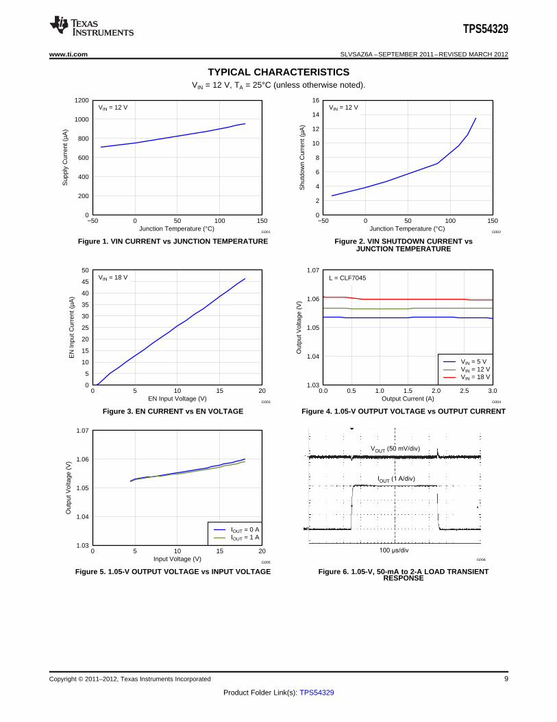
TYPICAL CHARACTERISTICSVIN = 12 V, TA = 25°C (unless otherwise noted).
Figure 7. START-UP WAVE FORM Figure 8. EFFICIENCY vs OUTPUT CURRENT
Figure 9. SWITCHING FREQUENCY vs INPUT VOLTAGE Figure 10. SWITCHING FREQUENCY vsOUTPUT CURRENT
Figure 11. Vfb VOLTAGE vs JUNCTION TEMPERATURE Figure 12. VOLTAGE RIPPLE AT OUTPUT (IO = 3 A)
10 Copyright © 2011–2012, Texas Instruments Incorporated
Product Folder Link(s): TPS54329
G013
400 ns/div
V = 1.05 VOUT
SW (5 V/div)
V (50 mV/div)IN
TPS54329
www.ti.com SLVSAZ6A –SEPTEMBER 2011–REVISED MARCH 2012
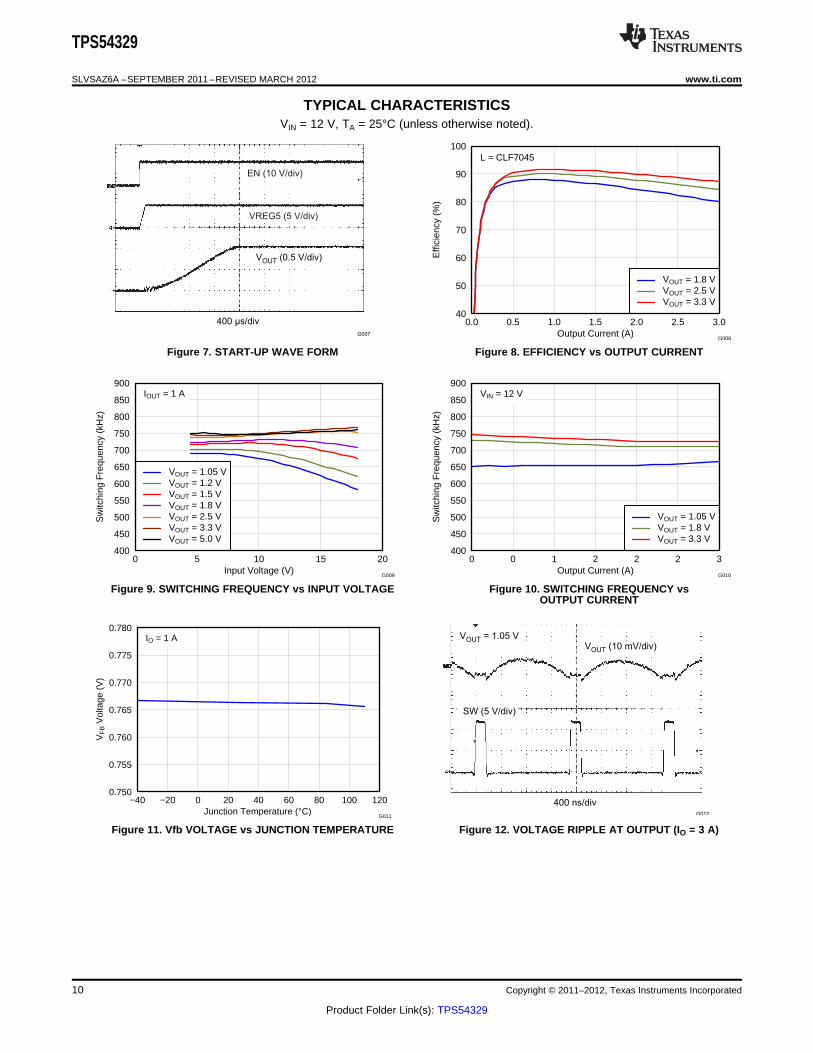
TYPICAL CHARACTERISTICSVIN = 12 V, TA = 25°C (unless otherwise noted).
Figure 13. VOLTAGE RIPPLE AT INPUT (IO = 3 A)
Copyright © 2011–2012, Texas Instruments Incorporated 11
Product Folder Link(s): TPS54329
U1
TPS54329DDA
V = 0.765 xOUT
R11 +
R2
æ ö÷ç ÷ç ÷÷çè ø
F =P
OUT OUT
1
2 L x Cp
TPS54329
SLVSAZ6A –SEPTEMBER 2011–REVISED MARCH 2012 www.ti.com
DESIGN GUIDE
Step By Step Design Procedure
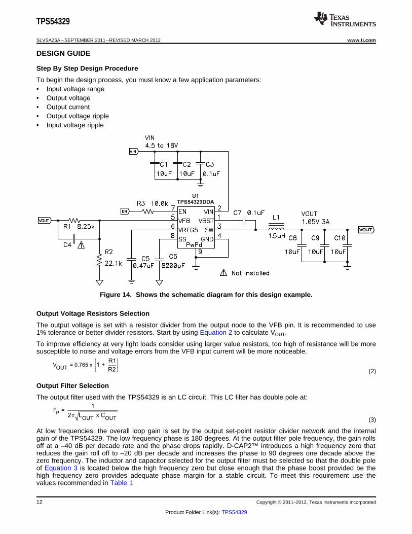
To begin the design process, you must know a few application parameters:• Input voltage range• Output voltage• Output current• Output voltage ripple• Input voltage ripple
Figure 14. Shows the schematic diagram for this design example.
Output Voltage Resistors Selection
The output voltage is set with a resistor divider from the output node to the VFB pin. It is recommended to use1% tolerance or better divider resistors. Start by using Equation 2 to calculate VOUT.
To improve efficiency at very light loads consider using larger value resistors, too high of resistance will be moresusceptible to noise and voltage errors from the VFB input current will be more noticeable.
(2)
Output Filter Selection
The output filter used with the TPS54329 is an LC circuit. This LC filter has double pole at:
(3)
At low frequencies, the overall loop gain is set by the output set-point resistor divider network and the internalgain of the TPS54329. The low frequency phase is 180 degrees. At the output filter pole frequency, the gain rollsoff at a –40 dB per decade rate and the phase drops rapidly. D-CAP2™ introduces a high frequency zero thatreduces the gain roll off to –20 dB per decade and increases the phase to 90 degrees one decade above thezero frequency. The inductor and capacitor selected for the output filter must be selected so that the double poleof Equation 3 is located below the high frequency zero but close enough that the phase boost provided be thehigh frequency zero provides adequate phase margin for a stable circuit. To meet this requirement use thevalues recommended in Table 1
12 Copyright © 2011–2012, Texas Instruments Incorporated
Product Folder Link(s): TPS54329
V VV IN(max) OUTOUT= xIPP V L x
IN(max) O SW
-I
f
lpp= +
Ipeak O 2
I
I I
2 2=
IPPLo(RMS) O
1+
12I I I
INOUT OUT=Co(RMS)
IN O SW
V x (V - V )
12 x V x L xI
f
TPS54329
www.ti.com SLVSAZ6A –SEPTEMBER 2011–REVISED MARCH 2012
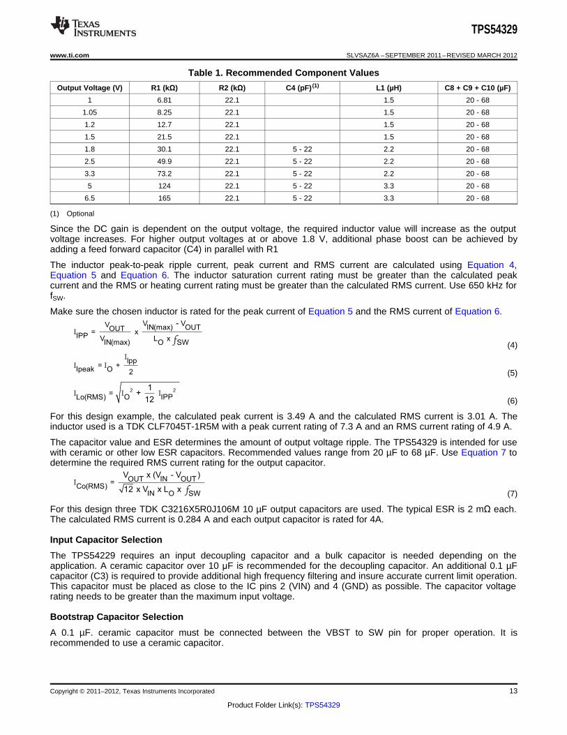
Table 1. Recommended Component Values
Output Voltage (V) R1 (kΩ) R2 (kΩ) C4 (pF) (1) L1 (µH) C8 + C9 + C10 (µF)
1 6.81 22.1 1.5 20 - 68
1.05 8.25 22.1 1.5 20 - 68
1.2 12.7 22.1 1.5 20 - 68
1.5 21.5 22.1 1.5 20 - 68
1.8 30.1 22.1 5 - 22 2.2 20 - 68
2.5 49.9 22.1 5 - 22 2.2 20 - 68
3.3 73.2 22.1 5 - 22 2.2 20 - 68
5 124 22.1 5 - 22 3.3 20 - 68
6.5 165 22.1 5 - 22 3.3 20 - 68
(1) Optional
Since the DC gain is dependent on the output voltage, the required inductor value will increase as the outputvoltage increases. For higher output voltages at or above 1.8 V, additional phase boost can be achieved byadding a feed forward capacitor (C4) in parallel with R1
The inductor peak-to-peak ripple current, peak current and RMS current are calculated using Equation 4,Equation 5 and Equation 6. The inductor saturation current rating must be greater than the calculated peakcurrent and the RMS or heating current rating must be greater than the calculated RMS current. Use 650 kHz forfSW.
Make sure the chosen inductor is rated for the peak current of Equation 5 and the RMS current of Equation 6.
(4)
(5)
(6)
For this design example, the calculated peak current is 3.49 A and the calculated RMS current is 3.01 A. Theinductor used is a TDK CLF7045T-1R5M with a peak current rating of 7.3 A and an RMS current rating of 4.9 A.
The capacitor value and ESR determines the amount of output voltage ripple. The TPS54329 is intended for usewith ceramic or other low ESR capacitors. Recommended values range from 20 µF to 68 µF. Use Equation 7 todetermine the required RMS current rating for the output capacitor.
(7)
For this design three TDK C3216X5R0J106M 10 µF output capacitors are used. The typical ESR is 2 mΩ each.The calculated RMS current is 0.284 A and each output capacitor is rated for 4A.
Input Capacitor Selection
The TPS54229 requires an input decoupling capacitor and a bulk capacitor is needed depending on theapplication. A ceramic capacitor over 10 μF is recommended for the decoupling capacitor. An additional 0.1 µFcapacitor (C3) is required to provide additional high frequency filtering and insure accurate current limit operation.This capacitor must be placed as close to the IC pins 2 (VIN) and 4 (GND) as possible. The capacitor voltagerating needs to be greater than the maximum input voltage.
Bootstrap Capacitor Selection
A 0.1 µF. ceramic capacitor must be connected between the VBST to SW pin for proper operation. It isrecommended to use a ceramic capacitor.
Copyright © 2011–2012, Texas Instruments Incorporated 13
Product Folder Link(s): TPS54329
TPS54329
SLVSAZ6A –SEPTEMBER 2011–REVISED MARCH 2012 www.ti.com
VREG5 Capacitor Selection
A 0.47 µF. ceramic capacitor must be connected between the VREG5 to GND pin for proper operation. It isrecommended to use a ceramic capacitor.
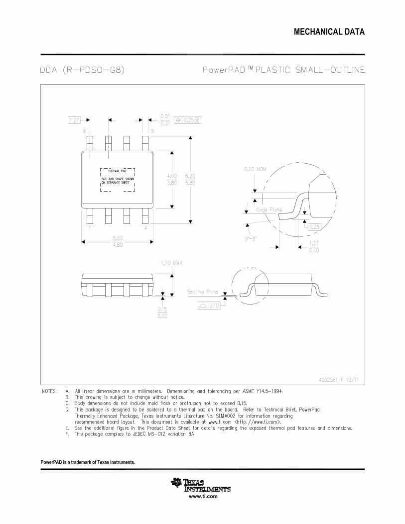
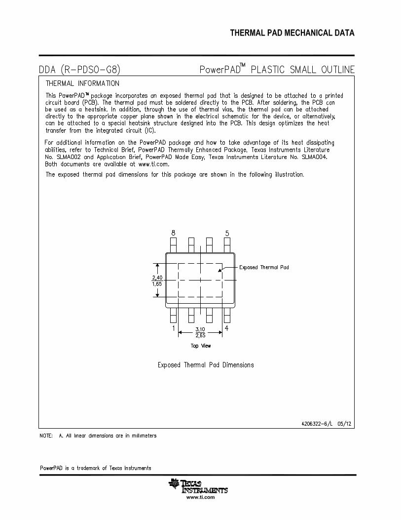
THERMAL INFORMATION
This 8-pin DDA package incorporates an exposed thermal pad that is designed to be directly to an externalheartsick. The thermal pad must be soldered directly to the printed board (PCB). After soldering, the PCB can beused as a heartsick. In addition, through the use of thermal vias, the thermal pad can be attached directly to theappropriate copper plane shown in the electrical schematic for the device, or alternatively, can be attached to aspecial heartsick structure designed into the PCB. This design optimizes the heat transfer from the integratedcircuit (IC).
For additional information on the exposed thermal pad and how to use the advantage of its heat dissipatingabilities, refer to Technical Brief, PowerPAD™ Thermally Enhanced Package, Texas Instruments Literature No.SLMA002 and Application Brief, PowerPAD™ Made Easy, Texas Instruments Literature No. SLMA004.
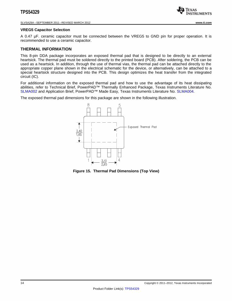
The exposed thermal pad dimensions for this package are shown in the following illustration.
Figure 15. Thermal Pad Dimensions (Top View)
14 Copyright © 2011–2012, Texas Instruments Incorporated
Product Folder Link(s): TPS54329
TPS54329
www.ti.com SLVSAZ6A –SEPTEMBER 2011–REVISED MARCH 2012
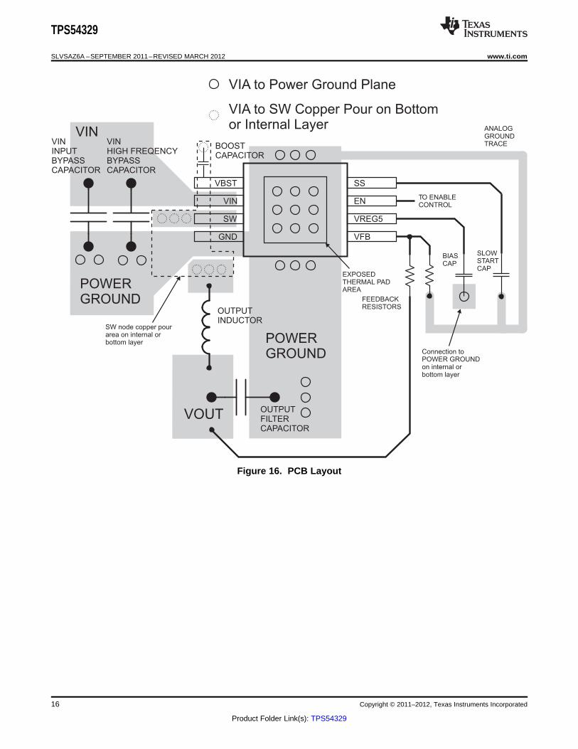
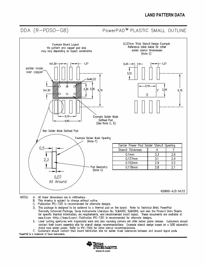
LAYOUT CONSIDERATIONS1. Keep the input switching current loop as small as possible.2. Keep the SW node as physically small and short as possible to minimize parasitic capacitance and
inductance and to minimize radiated emissions. Kelvin connections should be brought from the output to thefeedback pin of the device.
3. Keep analog and non-switching components away from switching components.4. Make a single point connection from the signal ground to power ground.5. Do not allow switching current to flow under the device.6. Keep the pattern lines for VIN and PGND broad.7. Exposed pad of device must be connected to PGND with solder.8. VREG5 capacitor should be placed near the device, and connected PGND.9. Output capacitor should be connected to a broad pattern of the PGND.10. Voltage feedback loop should be as short as possible, and preferably with ground shield.11. Lower resistor of the voltage divider which is connected to the VFB pin should be tied to analog ground
trace.12. Providing sufficient vias for VIN, SW and PGND connection.13. VIN input bypass capacitor and VIN high frequency bypass capacitor must be placed as near as possible to
the device.14. Performance based on four layer printed circuit board.
Copyright © 2011–2012, Texas Instruments Incorporated 15
Product Folder Link(s): TPS54329
VFB
VREG5
SS
GND
ENVIN
VBST
SW
EXPOSEDTHERMAL PADAREA
BOOSTCAPACITOR
VOUT
VIA to Power Ground Plane
OUTPUTINDUCTOR
OUTPUTFILTERCAPACITOR
SLOWSTARTCAP
ANALOGGROUNDTRACEVIN
INPUTBYPASSCAPACITOR
VIN
FEEDBACKRESISTORS
TO ENABLECONTROL
POWERGROUND
BIASCAP
Connection toPOWER GROUNDon internal orbottom layer
VINHIGH FREQENCYBYPASSCAPACITOR
VIA to SW Copper Pour on Bottomor Internal Layer
SW node copper pourarea on internal orbottom layer
POWERGROUND
TPS54329
SLVSAZ6A –SEPTEMBER 2011–REVISED MARCH 2012 www.ti.com
Figure 16. PCB Layout
16 Copyright © 2011–2012, Texas Instruments Incorporated
Product Folder Link(s): TPS54329
TPS54329
www.ti.com SLVSAZ6A –SEPTEMBER 2011–REVISED MARCH 2012
REVISION HISTORY
Changes from Original (September 2011) to Revision A Page
• Removed (SWIFT™) from the data sheet title ..................................................................................................................... 1
• Deleted from ELECTRICAL CHARACTERISTICS table, VLN5 and VLD5, deleted VVREG5 MIN and MAX values .................. 3
• Added in ELECTRICAL CHARACTERISTICS table, IVREG5, RDS(on)h, and RDS(on)l footnote references ................................ 3
• Added tOFF(MIN) footnote reference and deleted MAX value .................................................................................................. 4
• Deleted from ELECTRICAL CHARARACTERISTICS, UVLO MIN and MAX values ........................................................... 4
• Added TYPICAL CHARACTERISTICS Condition ................................................................................................................ 9
Copyright © 2011–2012, Texas Instruments Incorporated 17
Product Folder Link(s): TPS54329
PACKAGE OPTION ADDENDUM
www.ti.com 10-Dec-2020
Addendum-Page 1
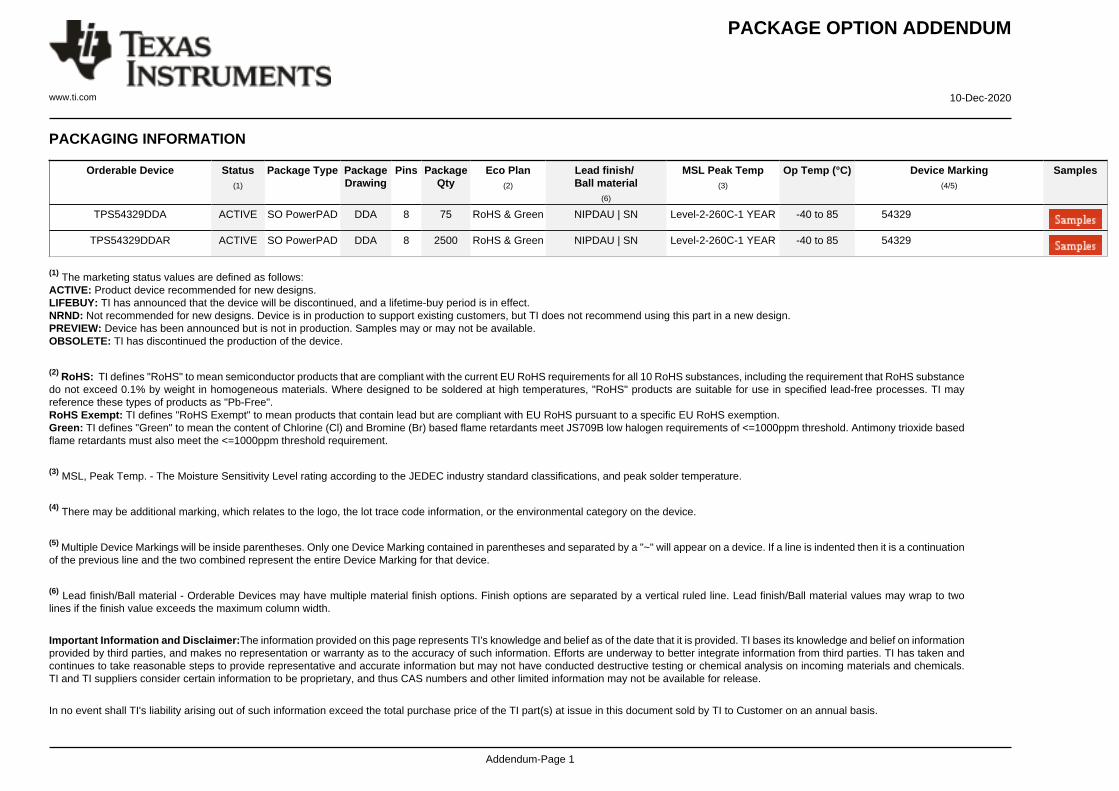
PACKAGING INFORMATION
Orderable Device Status(1)
Package Type PackageDrawing
Pins PackageQty
Eco Plan(2)
Lead finish/Ball material
(6)
MSL Peak Temp(3)
Op Temp (°C) Device Marking(4/5)
Samples
TPS54329DDA ACTIVE SO PowerPAD DDA 8 75 RoHS & Green NIPDAU | SN Level-2-260C-1 YEAR -40 to 85 54329
TPS54329DDAR ACTIVE SO PowerPAD DDA 8 2500 RoHS & Green NIPDAU | SN Level-2-260C-1 YEAR -40 to 85 54329
(1) The marketing status values are defined as follows:ACTIVE: Product device recommended for new designs.LIFEBUY: TI has announced that the device will be discontinued, and a lifetime-buy period is in effect.NRND: Not recommended for new designs. Device is in production to support existing customers, but TI does not recommend using this part in a new design.PREVIEW: Device has been announced but is not in production. Samples may or may not be available.OBSOLETE: TI has discontinued the production of the device.
(2) RoHS: TI defines "RoHS" to mean semiconductor products that are compliant with the current EU RoHS requirements for all 10 RoHS substances, including the requirement that RoHS substancedo not exceed 0.1% by weight in homogeneous materials. Where designed to be soldered at high temperatures, "RoHS" products are suitable for use in specified lead-free processes. TI mayreference these types of products as "Pb-Free".RoHS Exempt: TI defines "RoHS Exempt" to mean products that contain lead but are compliant with EU RoHS pursuant to a specific EU RoHS exemption.Green: TI defines "Green" to mean the content of Chlorine (Cl) and Bromine (Br) based flame retardants meet JS709B low halogen requirements of <=1000ppm threshold. Antimony trioxide basedflame retardants must also meet the <=1000ppm threshold requirement.
(3) MSL, Peak Temp. - The Moisture Sensitivity Level rating according to the JEDEC industry standard classifications, and peak solder temperature.
(4) There may be additional marking, which relates to the logo, the lot trace code information, or the environmental category on the device.
(5) Multiple Device Markings will be inside parentheses. Only one Device Marking contained in parentheses and separated by a "~" will appear on a device. If a line is indented then it is a continuationof the previous line and the two combined represent the entire Device Marking for that device.
(6) Lead finish/Ball material - Orderable Devices may have multiple material finish options. Finish options are separated by a vertical ruled line. Lead finish/Ball material values may wrap to twolines if the finish value exceeds the maximum column width.
Important Information and Disclaimer:The information provided on this page represents TI's knowledge and belief as of the date that it is provided. TI bases its knowledge and belief on informationprovided by third parties, and makes no representation or warranty as to the accuracy of such information. Efforts are underway to better integrate information from third parties. TI has taken andcontinues to take reasonable steps to provide representative and accurate information but may not have conducted destructive testing or chemical analysis on incoming materials and chemicals.TI and TI suppliers consider certain information to be proprietary, and thus CAS numbers and other limited information may not be available for release.
In no event shall TI's liability arising out of such information exceed the total purchase price of the TI part(s) at issue in this document sold by TI to Customer on an annual basis.
PACKAGE OPTION ADDENDUM
www.ti.com 10-Dec-2020
Addendum-Page 2
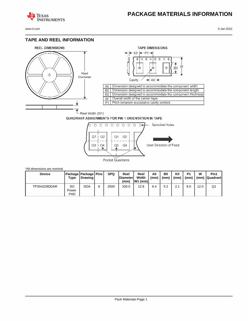
TAPE AND REEL INFORMATION
*All dimensions are nominal
Device PackageType
PackageDrawing
Pins SPQ ReelDiameter
(mm)
ReelWidth
W1 (mm)
A0(mm)
B0(mm)
K0(mm)
P1(mm)
W(mm)
Pin1Quadrant
TPS54329DDAR SOPower PAD
DDA 8 2500 330.0 12.8 6.4 5.2 2.1 8.0 12.0 Q1
PACKAGE MATERIALS INFORMATION
www.ti.com 5-Jan-2022
Pack Materials-Page 1
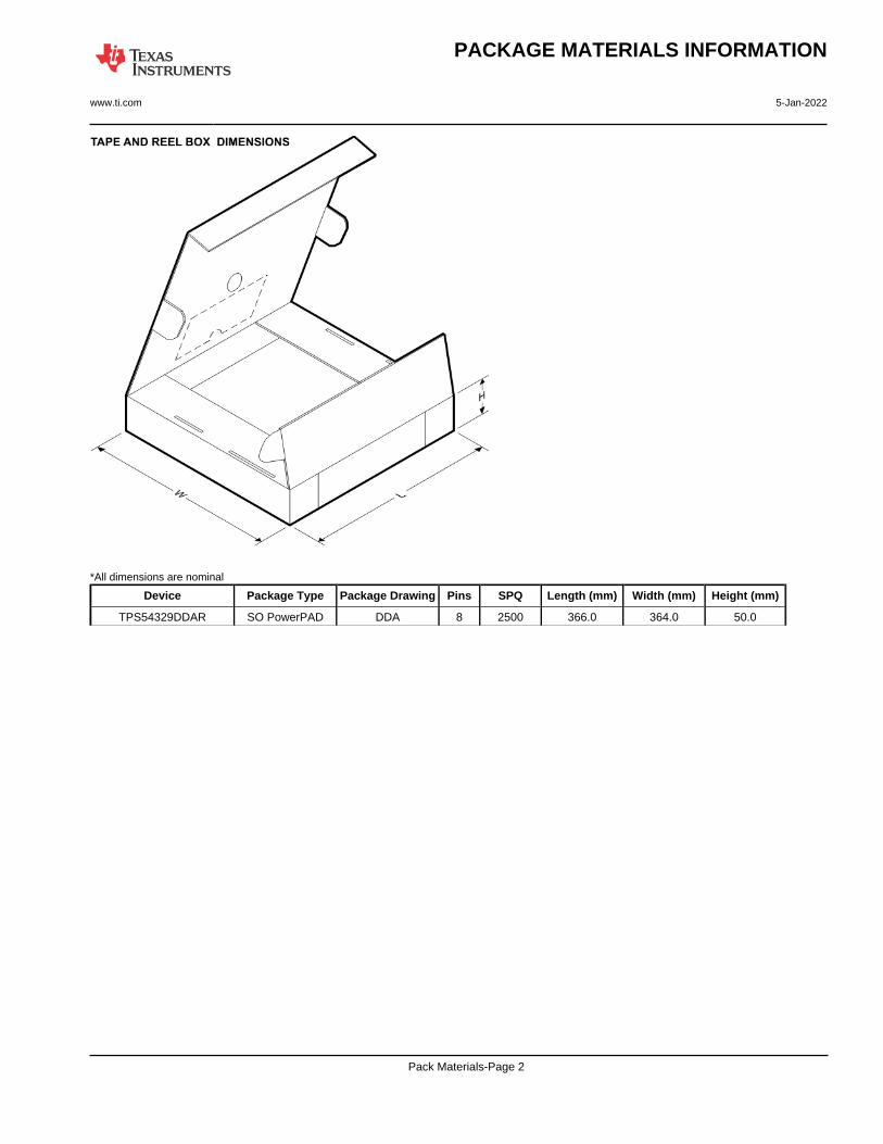
*All dimensions are nominal
Device Package Type Package Drawing Pins SPQ Length (mm) Width (mm) Height (mm)
TPS54329DDAR SO PowerPAD DDA 8 2500 366.0 364.0 50.0
PACKAGE MATERIALS INFORMATION
www.ti.com 5-Jan-2022
Pack Materials-Page 2
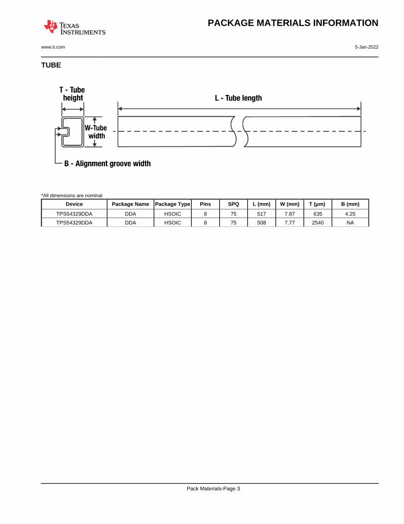
TUBE
*All dimensions are nominal
Device Package Name Package Type Pins SPQ L (mm) W (mm) T (µm) B (mm)
TPS54329DDA DDA HSOIC 8 75 517 7.87 635 4.25
TPS54329DDA DDA HSOIC 8 75 508 7.77 2540 NA
PACKAGE MATERIALS INFORMATION
www.ti.com 5-Jan-2022
Pack Materials-Page 3
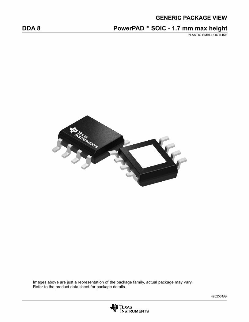
GENERIC PACKAGE VIEW
Images above are just a representation of the package family, actual package may vary.Refer to the product data sheet for package details.
DDA 8 PowerPAD TM SOIC - 1.7 mm max heightPLASTIC SMALL OUTLINE
4202561/G

IMPORTANT NOTICE AND DISCLAIMERTI PROVIDES TECHNICAL AND RELIABILITY DATA (INCLUDING DATA SHEETS), DESIGN RESOURCES (INCLUDING REFERENCE DESIGNS), APPLICATION OR OTHER DESIGN ADVICE, WEB TOOLS, SAFETY INFORMATION, AND OTHER RESOURCES “AS IS” AND WITH ALL FAULTS, AND DISCLAIMS ALL WARRANTIES, EXPRESS AND IMPLIED, INCLUDING WITHOUT LIMITATION ANY IMPLIED WARRANTIES OF MERCHANTABILITY, FITNESS FOR A PARTICULAR PURPOSE OR NON-INFRINGEMENT OF THIRD PARTY INTELLECTUAL PROPERTY RIGHTS.These resources are intended for skilled developers designing with TI products. You are solely responsible for (1) selecting the appropriate TI products for your application, (2) designing, validating and testing your application, and (3) ensuring your application meets applicable standards, and any other safety, security, regulatory or other requirements.These resources are subject to change without notice. TI grants you permission to use these resources only for development of an application that uses the TI products described in the resource. Other reproduction and display of these resources is prohibited. No license is granted to any other TI intellectual property right or to any third party intellectual property right. TI disclaims responsibility for, and you will fully indemnify TI and its representatives against, any claims, damages, costs, losses, and liabilities arising out of your use of these resources.TI’s products are provided subject to TI’s Terms of Sale or other applicable terms available either on ti.com or provided in conjunction with such TI products. TI’s provision of these resources does not expand or otherwise alter TI’s applicable warranties or warranty disclaimers for TI products.TI objects to and rejects any additional or different terms you may have proposed. IMPORTANT NOTICE
Mailing Address: Texas Instruments, Post Office Box 655303, Dallas, Texas 75265Copyright © 2022, Texas Instruments Incorporated
Related Documents