1 Equipment Architecture 1-1 ............................................................................... 2 Cabinet 2-1 ........................................................................................................... 2.1 Types 2-1 ...................................................................................................... 2.2 Technical Parameters 2-3 ............................................................................ 3 Subrack 3-1 .......................................................................................................... 3.1 Structure 3-2 ................................................................................................. 3.2 Technical Parameters 3-5 ............................................................................ 4 Boards 4-1 ........................................................................................................... 4.1 Classified Board Description 4-1 .................................................................. 4.2 Board Appearance 4-4 ................................................................................. 4.3 SL64 4-5 ....................................................................................................... 4.3.1 Functions and Principles 4-5 ................................................................ 4.3.2 Front Panel 4-7 .................................................................................... 4.3.3 Interface 4-8 ......................................................................................... 4.3.4 Board Configuration 4-8 ....................................................................... 4.3.5 Technical Parameters 4-8 .................................................................... 4.4 SL16 4-10 ....................................................................................................... 4.4.1 Functions and Principles 4-10 ................................................................ 4.4.2 Front Panel 4-12 .................................................................................... 4.4.3 Interface 4-13 ......................................................................................... 4.4.4 Board Configuration 4-13 ....................................................................... 4.4.5 Technical Parameters 4-13 .................................................................... 4.5 SLQ4/SLD4/SL4 4-15 ..................................................................................... 4.5.1 Functions and Principles 4-15 ................................................................ 4.5.2 Front Panel 4-16 .................................................................................... 4.5.3 Interface 4-19 ......................................................................................... 4.5.4 Board Configuration 4-19 ....................................................................... 4.5.5 Technical Parameters 4-19 .................................................................... 4.6 SLQ1/SL1 4-21 ............................................................................................... 4.6.1 Functions and Principles 4-21 ................................................................ 4.6.2 Front Panel 4-22 .................................................................................... 4.6.3 Interface 4-25 ......................................................................................... 4.6.4 Board Configuration 4-25 ....................................................................... 4.6.5 Technical Parameters 4-25 .................................................................... 4.7 SEP1/EU08/OU08/EU04/TSB8/TSB4 4-27 .................................................... 4.7.1 Functions and Principles 4-28 ................................................................ 4.7.2 Front Panel 4-30 .................................................................................... 4.7.3 Interface 4-32 .........................................................................................

31250187-Hardware Description Manual
Oct 22, 2014
Welcome message from author
This document is posted to help you gain knowledge. Please leave a comment to let me know what you think about it! Share it to your friends and learn new things together.
Transcript
1 Equipment Architecture 1-1...............................................................................
2 Cabinet 2-1...........................................................................................................
2.1 Types 2-1......................................................................................................2.2 Technical Parameters 2-3............................................................................
3 Subrack 3-1..........................................................................................................
3.1 Structure 3-2.................................................................................................3.2 Technical Parameters 3-5............................................................................
4 Boards 4-1...........................................................................................................
4.1 Classified Board Description 4-1..................................................................4.2 Board Appearance 4-4.................................................................................4.3 SL64 4-5.......................................................................................................
4.3.1 Functions and Principles 4-5................................................................4.3.2 Front Panel 4-7....................................................................................4.3.3 Interface 4-8.........................................................................................4.3.4 Board Configuration 4-8.......................................................................4.3.5 Technical Parameters 4-8....................................................................
4.4 SL16 4-10.......................................................................................................4.4.1 Functions and Principles 4-10................................................................4.4.2 Front Panel 4-12....................................................................................4.4.3 Interface 4-13.........................................................................................4.4.4 Board Configuration 4-13.......................................................................4.4.5 Technical Parameters 4-13....................................................................
4.5 SLQ4/SLD4/SL4 4-15.....................................................................................4.5.1 Functions and Principles 4-15................................................................4.5.2 Front Panel 4-16....................................................................................4.5.3 Interface 4-19.........................................................................................4.5.4 Board Configuration 4-19.......................................................................4.5.5 Technical Parameters 4-19....................................................................
4.6 SLQ1/SL1 4-21...............................................................................................4.6.1 Functions and Principles 4-21................................................................4.6.2 Front Panel 4-22....................................................................................4.6.3 Interface 4-25.........................................................................................4.6.4 Board Configuration 4-25.......................................................................4.6.5 Technical Parameters 4-25....................................................................
4.7 SEP1/EU08/OU08/EU04/TSB8/TSB4 4-27....................................................4.7.1 Functions and Principles 4-28................................................................4.7.2 Front Panel 4-30....................................................................................4.7.3 Interface 4-32.........................................................................................
4.7.4 Board Configuration 4-32.......................................................................4.7.5 Technical Parameters 4-33....................................................................
4.8 SPQ4/MU04 4-35...........................................................................................4.8.1 Functions and Principles 4-35................................................................4.8.2 Front Panel 4-37....................................................................................4.8.3 Interface 4-39.........................................................................................4.8.4 Board Configuration 4-40.......................................................................4.8.5 Technical Parameters 4-41....................................................................
4.9 PD3/PL3/D34S/C34S 4-42.............................................................................4.9.1 Functions and Principles 4-42................................................................4.9.2 Front Panel 4-44....................................................................................4.9.3 Interface 4-46.........................................................................................4.9.4 Board Configuration 4-46.......................................................................4.9.5 Technical Specifications 4-47................................................................
4.10 PQ1/PQM/D75S/D12S/D12B 4-48...............................................................4.10.1 Functions and Principles 4-48..............................................................4.10.2 Front Panel 4-49..................................................................................4.10.3 Interface 4-52.......................................................................................4.10.4 DIP Switch and Jumper 4-53...............................................................4.10.5 Board Configuration 4-53.....................................................................4.10.6 Technical Parameters 4-54..................................................................
4.11 EGS2 4-55....................................................................................................4.11.1 Functions and Principles 4-55..............................................................4.11.2 Front Panel 4-57..................................................................................4.11.3 Interface 4-59.......................................................................................4.11.4 DIP Switch and Jumper 4-59...............................................................4.11.5 Board Configuration 4-59.....................................................................4.11.6 Technical Parameters 4-60..................................................................
4.12 EFS4/EFS0/ETF8 4-61.................................................................................4.12.1 Functions and Principles 4-61..............................................................4.12.2 Front Panel 4-63..................................................................................4.12.3 Interface 4-65.......................................................................................4.12.4 DIP Switch and Jumper 4-65...............................................................4.12.5 Board Configuration 4-65.....................................................................4.12.6 Technical Parameters 4-66..................................................................
4.13 BA2/BPA 4-67..............................................................................................4.13.1 Functions and Principles 4-67..............................................................4.13.2 Front Panel 4-69..................................................................................4.13.3 Interface 4-71.......................................................................................4.13.4 Technical Parameters 4-72..................................................................
4.14 DCU 4-73......................................................................................................
4.14.1 Functions and Principles 4-73..............................................................4.14.2 Front Panel 4-74..................................................................................4.14.3 Interface 4-77.......................................................................................4.14.4 Technical Parameters 4-78..................................................................
4.15 GXCS/EXCS 4-79........................................................................................4.15.1 Functions and Principles 4-79..............................................................4.15.2 Front Panel 4-81..................................................................................4.15.3 Interface 4-83.......................................................................................4.15.4 DIP Switch and Jumper 4-83...............................................................4.15.5 Board Configuration 4-83.....................................................................4.15.6 Technical Parameters 4-86..................................................................
4.16 SCC 4-87......................................................................................................4.16.1 Functions and Principles 4-87..............................................................4.16.2 Front Panel 4-90..................................................................................4.16.3 Interface 4-92.......................................................................................4.16.4 Technical Parameters 4-92..................................................................
4.17 AUX 4-93......................................................................................................4.17.1 Functions and Principles 4-93..............................................................4.17.2 Front Panel 4-94..................................................................................4.17.3 DIP Switch and Jumper 4-97...............................................................4.17.4 Technical Parameters 4-97..................................................................
4.18 PIU 4-99.......................................................................................................4.18.1 Functions and Principles 4-99..............................................................4.18.2 Front Panel 4-100..................................................................................4.18.3 Interface 4-101.......................................................................................4.18.4 DIP Switch and Jumper 4-101...............................................................4.18.5 Technical Parameters 4-101..................................................................
4.19 FAN 4-102......................................................................................................4.19.1 Functions and Principles 4-102..............................................................4.19.2 Front Panel 4-104..................................................................................4.19.3 Interface 4-104.......................................................................................4.19.4 Technical Parameters 4-104..................................................................
5 Cables 5-1............................................................................................................
5.1 Internal Cables 5-1.......................................................................................5.1.1 Subrack Power Cable 5-1....................................................................5.1.2 Indicator and Alarm Concatenating Cables between Subracks 5-2.....5.1.3 Cabinet Indicator Cable 5-4.................................................................5.1.4 Cabinet Door Grounding Cable 5-5......................................................
5.2 External Cables 5-7......................................................................................5.2.1 Alarm Concatenating Cable 5-7...........................................................
5.2.2 Boolean Input/Output Cable 5-8...........................................................5.2.3 HUB Power Cable 5-10..........................................................................5.2.4 OAM Serial Port Cable 5-11...................................................................5.2.5 S1~4/F1/F&f Cable 5-12........................................................................5.2.6 RS232/422 Serial Port Cable 5-13.........................................................5.2.7 Straight Through Cable 5-14..................................................................5.2.8 Crossover Cable 5-16............................................................................5.2.9 75degrees Angle Straight Through Cable 5-17......................................5.2.10 75degrees Angle Crossover Cable 5-18..............................................5.2.11 Transfer Cable of 75degrees Angle Straight Through Cable 5-19.......5.2.12 Ordinary Telephone Line 5-21.............................................................5.2.13 -48V Cabinet Power Cable/Cabinet BGND Power Cable/Cabinet PGND Power Cable 5-22...................................................................5.2.14 75ohm E1 Cable 5-23..........................................................................5.2.15 75ohm E1 Self-Loop Test Cable 5-24..................................................5.2.16 120ohm E1 Cable 5-26........................................................................5.2.17 E3/DS3 Cable 5-28..............................................................................5.2.18 STM-1 Cable 5-28................................................................................5.2.19 Clock Cable 5-29..................................................................................5.2.20 1/2-Channel Clock Transfer Cable 5-31...............................................
A Indicator Description for Equipment and Board A-1.......................................
A.1 Cabinet Indicator Description A-1.................................................................A.2 Board Indicator Description A-2....................................................................
B Power Consumption and Weight B-1................................................................
C Acronyms and Abbreviations C-1.....................................................................
HUAWEI
OptiX OSN 3500 STM-64/STM-16 Intelligent Optical Transmission Platform Hardware Description Manual
V100R001

OptiX OSN 3500 STM-64/STM-16
Intelligent Optical Transmission Platform
Hardware Description Manual
Manual Version T2-042587-20040215-C-1.10
Product Version V100R001
BOM 31250187
Huawei Technologies Co., Ltd. provides customers with comprehensive technical support and service. Please feel free to contact our local office or company headquarters.
Huawei Technologies Co., Ltd.
Address: Administration Building, Huawei Technologies Co., Ltd.,
Bantian, Longgang District, Shenzhen, P. R. China
Postal Code: 518129
Website: http://www.huawei.com
Email: [email protected]

Copyright © 2004 Huawei Technologies Co., Ltd.
All Rights Reserved
No part of this manual may be reproduced or transmitted in any form or by any means without prior written consent of Huawei Technologies Co., Ltd.
Trademarks
, HUAWEI, C&C08, EAST8000, HONET, , ViewPoint, INtess, ETS, DMC,
TELLIN, InfoLink, Netkey, Quidway, SYNLOCK, Radium, M900/M1800, TELESIGHT, Quidview, Musa, Airbridge, Tellwin, Inmedia, VRP, DOPRA, iTELLIN, HUAWEI OptiX, C&C08 iNET, NETENGINE, OptiX, iSite, U-SYS, iMUSE, OpenEye, Lansway, SmartAX, infoX, TopEng are trademarks of Huawei Technologies Co., Ltd.
All other trademarks mentioned in this manual are the property of their respective holders.
Notice
The information in this manual is subject to change without notice. Every effort has been made in the preparation of this manual to ensure accuracy of the contents, but all statements, information, and recommendations in this manual do not constitute the warranty of any kind, express or implied.
OptiX OSN 3500 HDM
About This Manual
Release Notes
This manual is for OptiX OSN 3500 STM-64/STM-16 Intelligent Optical Transmission Platform, Version V100R001.
Related Manuals
Manual Volume Usage
System Description Introduces the functionality, structure, performance, specifications, and theory of the product. OptiX OSN 3500 STM-64/STM-16 Intelligent
Optical Transmission Platform Technical Manual Networking and
Application Introduces the networking, configuration and application of the product.
OptiX OSN 3500 STM-64/STM-16 Intelligent Optical Transmission Platform Hardware Description Manual
Introduces the hardware of the product, including cabinet, subrack, power, fan, board, and a variety of interfaces.
OptiX OSN 3500 STM-64/STM-16 Intelligent Optical Transmission Platform Installation Manual
Guides the on-site installation of the product and provides the information of the structural parts.
Troubleshooting OptiX OSN 3500 STM-64/STM-16 Intelligent Optical Transmission Platform Maintenance Manual Alarm and
Performance Event
Guides the analysis and troubleshooting of common faults.
About This Manual OptiX OSN 3500 HDM
Manual Volume Usage Routine
Maintenance
OptiX OSN 3500 STM-64/STM-16 Intelligent Optical Transmission Platform Electronic Documentation (CD-ROM)
Covers all the preceding manuals. Acrobat Reader is attached.
Organization
The manual has the following organization: Chapter Description Chapter 1 Equipment Architecture
Introduces the Architecture of OptiX OSN 3500.
Chapter 2 Cabinet Introduces the category of the cabinet and cabinet parameter.
Chapter 3 Subrack Introduces the subrack configuration and the boards of OptiX OSN 3500.
Chapter 4 Boards Introduces the boards in terms of function, theory, front panel, and technical specifications.
Chapter 5 Cables Introduces the cables of OptiX OSN 3500.
Appendix A ~ Appendix C Includes three appendices: Table of Indicators, Power Consumption and Weight of Boards, and Abbreviations.
The appendices provide a quick search means to useful information.
Intended Audience
This manual is for:
Network administrator
Maintenance engineer
Provisioning engineer
About This Manual OptiX OSN 3500 HDM
Conventions
The following conventions are used throughout this publication. Symbol Description
Means reader be careful. In this situation, you might do something that could result in equipment damage or loss of data.
Means reader be careful. The equipment is static-sensitive.
Means reader be careful. In this situation, the high voltage could result in harm to yourself or others.
Means reader be careful. In this situation, the strong laser beam could result in harm to yourself or others.
Means reader take note. Notes contain helpful suggestions or useful background information.
Release Upgrade Description
Release Release upgrade description
T2-042587-20040215-C-1.10 This manual is the first release.
OptiX OSN 3500 HDM
i
Contents
1 Equipment Architecture
2 Cabinet
2.1 Types 2-1 2.2 Technical Parameters 2-3
3 Subrack
3.1 Structure 3-2 3.2 Technical Parameters 3-5
4 Boards
4.1 Classified Board Description 4-1 4.2 Board Appearance 4-4 4.3 SL64 4-5
4.3.1 Functions and Principles 4-5 4.3.2 Front Panel 4-7 4.3.3 Interface 4-8 4.3.4 Board Configuration 4-8 4.3.5 Technical Parameters 4-8
4.4 SL16 4-10 4.4.1 Functions and Principles 4-10 4.4.2 Front Panel 4-12 4.4.3 Interface 4-13 4.4.4 Board Configuration 4-13 4.4.5 Technical Parameters 4-13
4.5 SLQ4/SLD4/SL4 4-15 4.5.1 Functions and Principles 4-15 4.5.2 Front Panel 4-16
OptiX OSN 3500 HDM
ii
Contents
4.5.3 Interface 4-19 4.5.4 Board Configuration 4-19 4.5.5 Technical Parameters 4-19
4.6 SLQ1/SL1 4-21 4.6.1 Functions and Principles 4-21 4.6.2 Front Panel 4-22 4.6.3 Interface 4-25 4.6.4 Board Configuration 4-25 4.6.5 Technical Parameters 4-25
4.7 SEP1/EU08/OU08/EU04/TSB8/ TSB4 4-27 4.7.1 Functions and Principles 4-28 4.7.2 Front Panel 4-30 4.7.3 Interface 4-32 4.7.4 Board Configuration 4-32 4.7.5 Technical Parameters 4-33
4.8 SPQ4/MU04 4-35 4.8.1 Functions and Principles 4-35 4.8.2 Front Panel 4-37 4.8.3 Interface 4-39 4.8.4 Board Configuration 4-40 4.8.5 Technical Parameters 4-41
4.9 PD3/PL3/D34S 4-42 4.9.1 Functions and Principles 4-42 4.9.2 Front Panel 4-44 4.9.3 Interface 4-46 4.9.4 Board Configuration 4-46 4.9.5 Technical Specifications 4-47
4.10 PQ1/PQM/D75S/D12S/D12B 4-48 4.10.1 Functions and Principles 4-48 4.10.2 Front Panel 4-49 4.10.3 Interface 4-52 4.10.4 DIP Switch and Jumper 4-53 4.10.5 Board Configuration 4-53
OptiX OSN 3500 HDM
iii
Contents
4.10.6 Technical Parameters 4-54 4.11 EGS2 4-55
4.11.1 Functions and Principles 4-55 4.11.2 Front Panel 4-57 4.11.3 Interface 4-59 4.11.4 DIP Switch and Jumper 4-59 4.11.5 Board Configuration 4-59 4.11.6 Technical Parameters 4-60
4.12 EFS4/EFS0/ETF8 4-61 4.12.1 Functions and Principles 4-61 4.12.2 Front Panel 4-63 4.12.3 Interface 4-65 4.12.4 DIP Switch and Jumper 4-65 4.12.5 Board Configuration 4-65 4.12.6 Technical Parameters 4-66
4.13 BA2/BPA 4-67 4.13.1 Functions and Principles 4-67 4.13.2 Front Panel 4-69 4.13.3 Interface 4-71 4.13.4 Technical Parameters 4-72
4.14 DCU 4-73 4.14.1 Functions and Principles 4-73 4.14.2 Front Panel 4-74 4.14.3 Interface 4-77 4.14.4 Technical Parameters 4-78
4.15 GXCS/EXCS 4-79 4.15.1 Functions and Principles 4-79 4.15.2 Front Panel 4-81 4.15.3 Interface 4-83 4.15.4 DIP Switch and Jumper 4-83 4.15.5 Board Configuration 4-83 4.15.6 Technical Parameters 4-86
4.16 SCC 4-87
OptiX OSN 3500 HDM
iv
Contents
4.16.1 Functions and Principles 4-87 4.16.2 Front Panel 4-90 4.16.3 Interface 4-92 4.16.4 Technical Parameters 4-92
4.17 AUX 4-93 4.17.1 Functions and Principles 4-93 4.17.2 Front Panel 4-94 4.17.3 DIP Switch and Jumper 4-97 4.17.4 Technical Parameters 4-97
4.18 PIU 4-99 4.18.1 Functions and Principles 4-99 4.18.2 Front Panel 4-100 4.18.3 Interface 4-101 4.18.4 DIP Switch and Jumper 4-101 4.18.5 Technical Parameters 4-101
4.19 FAN 4-102 4.19.1 Functions and Principles 4-102 4.19.2 Front Panel 4-104 4.19.3 Interface 4-104 4.19.4 Technical Parameters 4-104
5 Cables
5.1 Internal Cables 5-1 5.1.1 Subrack Power Cable 5-1 5.1.2 Indicator and Alarm Concatenating Cables between Subracks 5-2 5.1.3 Cabinet Indicator Cable 5-4 5.1.4 Cabinet Door Grounding Cable 5-5
5.2 External Cables 5-7 5.2.1 Alarm Concatenating Cable 5-7 5.2.2 Boolean Input/Output Cable 5-8
OptiX OSN 3500 HDM
v
Contents
5.2.3 HUB Power Cable 5-10 5.2.4 OAM Serial Port Cable 5-11 5.2.5 S1 ~ 4/F1/F&f Cable 5-12 5.2.6 RS232/422 Serial Port Cable 5-13 5.2.7 Straight Through Cable 5-14 5.2.8 Crossover Cable 5-16 5.2.9 75° Angle Straight Through Cable 5-17 5.2.10 75° Angle Crossover Cable 5-18 5.2.11 Transfer Cable of 75° Angle Straight Through Cable 5-19 5.2.12 Ordinary Telephone Line 5-21 5.2.13 -48V Cabinet Power Cable/Cabinet BGND Power Cable/Cabinet PGND Power Cable 5-22 5.2.14 75Ω E1 Cable 5-23 5.2.15 75Ω E1 Self-Loop Test Cable 5-24 5.2.16 120Ω E1 Cable 5-26 5.2.17 E3/DS3 Cable 5-28 5.2.18 STM-1 Cable 5-28 5.2.19 Clock Cable 5-29 5.2.20 1/2-Channel Clock Transfer Cable 5-31
A Indicator Description for Equipment and Board
A.1 Cabinet Indicator Description A-1 A.2 Board Indicator Description A-2
B Power Consumption
C Acronyms and Abbreviations

OptiX OSN 3500 HDM
1-1
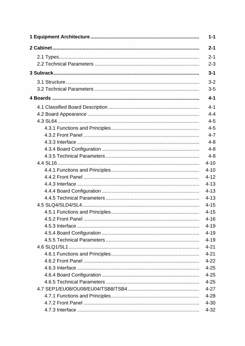
1 Equipment Architecture
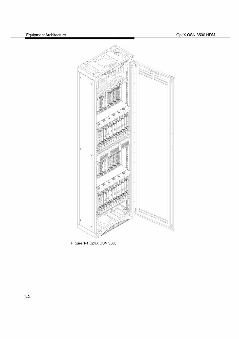
The OptiX OSN 3500 is composed of cabinet, power supply unit, fan unit, subrack, boards and cables, as shown in Figure 1-1.
Equipment Architecture OptiX OSN 3500 HDM
1-2
Figure 1-1 OptiX OSN 3500
OptiX OSN 3500 HDM
2-1
2 Cabinet
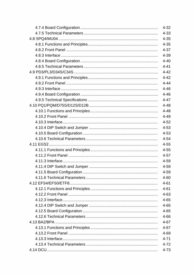
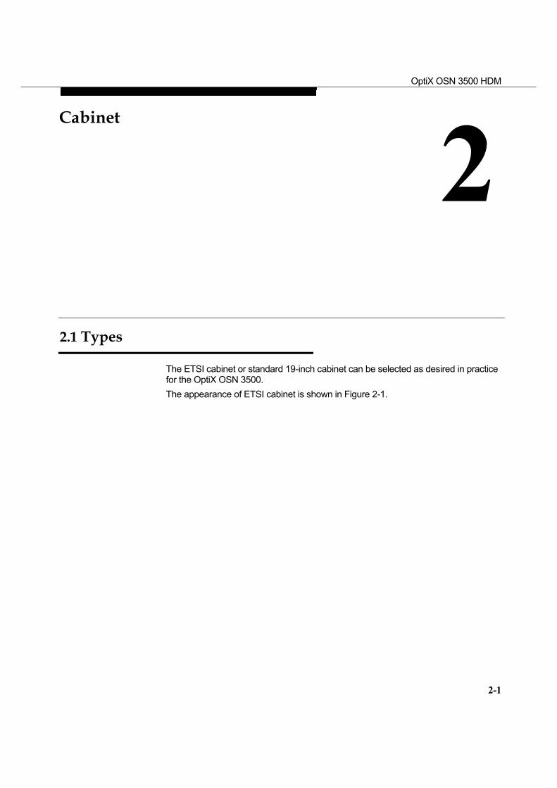
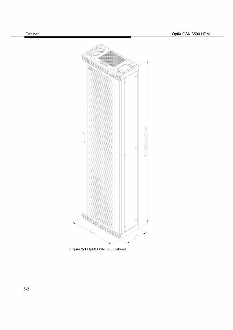
2.1 Types
The ETSI cabinet or standard 19-inch cabinet can be selected as desired in practice for the OptiX OSN 3500. The appearance of ETSI cabinet is shown in Figure 2-1.
Cabinet OptiX OSN 3500 HDM
2-2
Figure 2-1 OptiX OSN 3500 cabinet
Cabinet OptiX OSN 3500 HDM
2-3
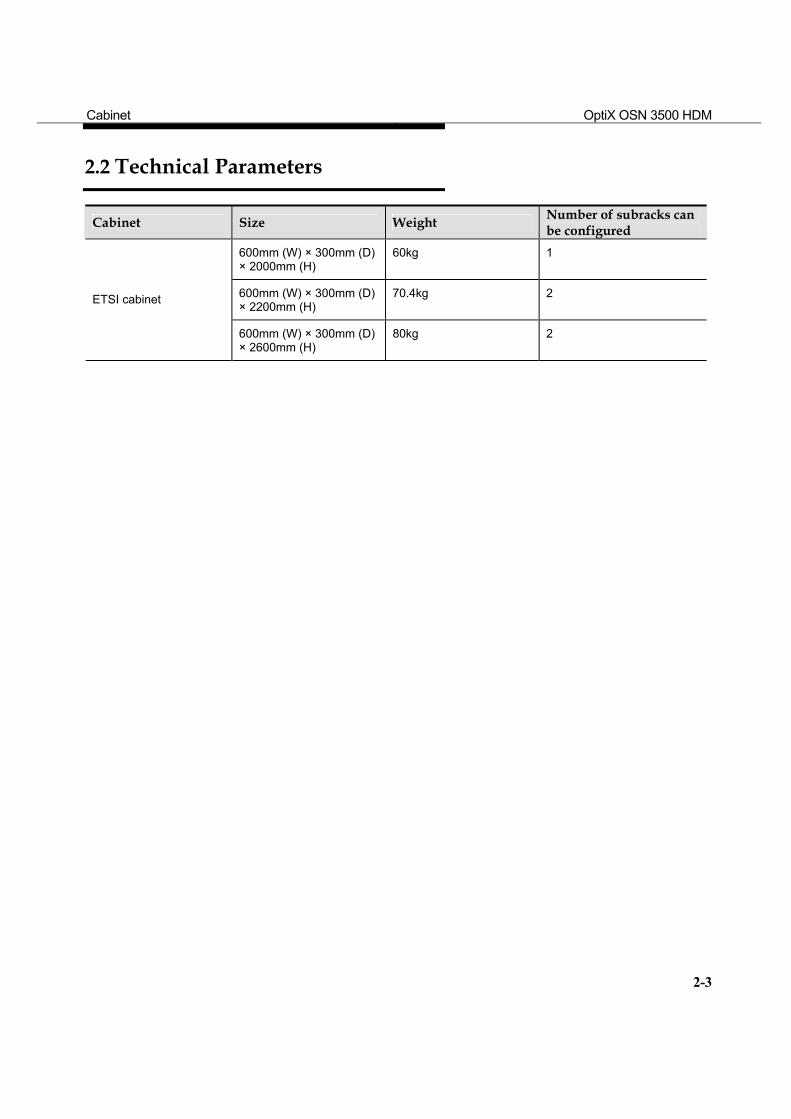
2.2 Technical Parameters
Cabinet Size Weight Number of subracks can be configured
600mm (W) × 300mm (D) × 2000mm (H)
60kg 1
600mm (W) × 300mm (D) × 2200mm (H)
70.4kg 2 ETSI cabinet
600mm (W) × 300mm (D) × 2600mm (H)
80kg 2
OptiX OSN 3500 HDM
3-1
3 Subrack
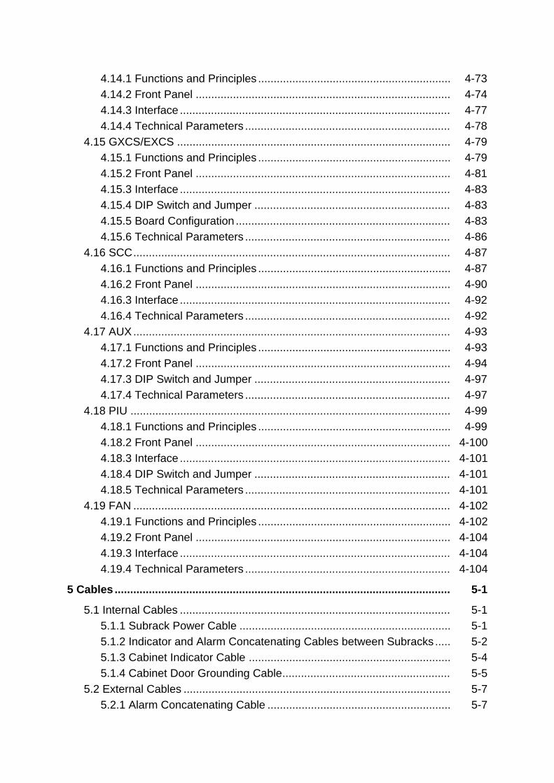
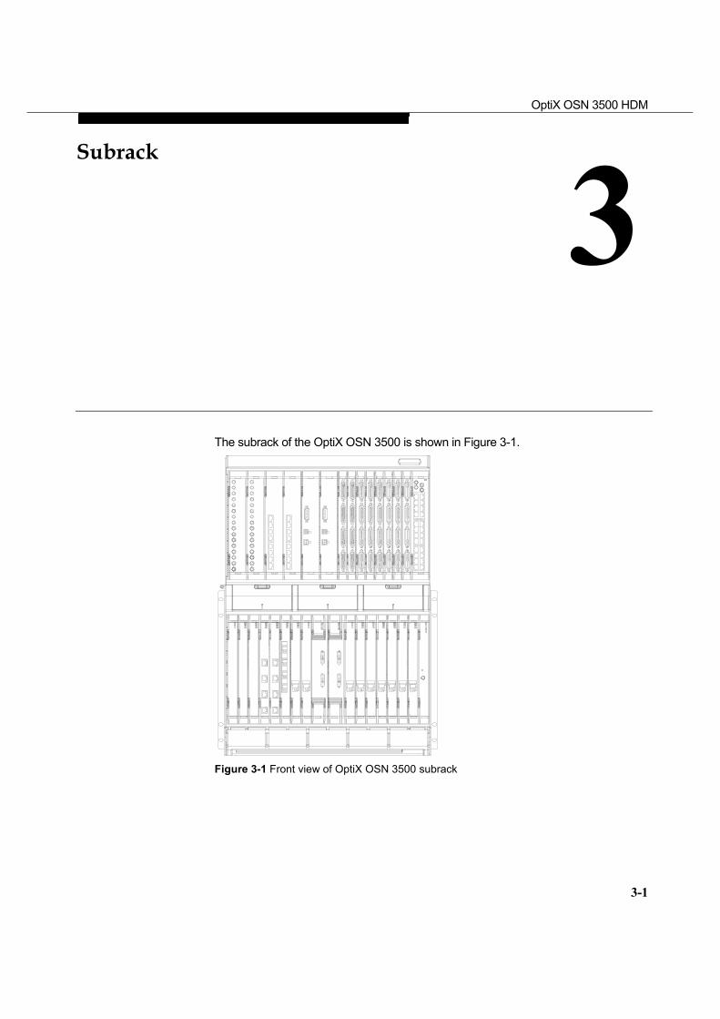
The subrack of the OptiX OSN 3500 is shown in Figure 3-1.
Figure 3-1 Front view of OptiX OSN 3500 subrack
Subrack OptiX OSN 3500 HDM
3-2
3.1 Structure
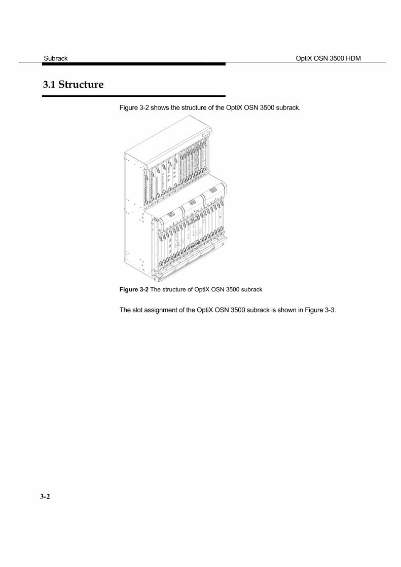
Figure 3-2 shows the structure of the OptiX OSN 3500 subrack.
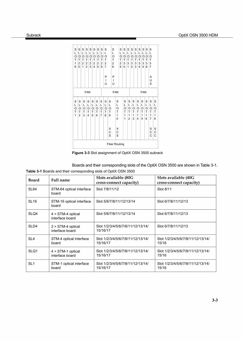
Figure 3-2 The structure of OptiX OSN 3500 subrack The slot assignment of the OptiX OSN 3500 subrack is shown in Figure 3-3.
Subrack OptiX OSN 3500 HDM
3-3
Fiber Routing
SLOT1
SLOT2
SLOT3
SLOT4
SLOT5
SLOT6
SLOT7
SLOT8
SLOT9
SLOT10
SLOT11
SLOT12
SLOT13
SLOT14
SLOT15
SLOT16
SLOT17
SLOT18
SLOT27
SLOT19
SLOT20
SLOT21
SLOT22
SLOT23
SLOT24
SLOT25
SLOT26
SLOT37
SLOT29
SLOT30
SLOT31
SLOT32
SLOT33
SLOT34
SLOT36
SLOT35
SLOT28
FAN FAN FAN
PIU
PIU
AUX
SCC
SCC
XCS
XCS
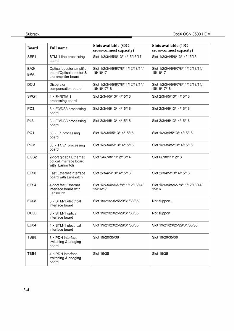
Figure 3-3 Slot assignment of OptiX OSN 3500 subrack Boards and their corresponding slots of the OptiX OSN 3500 are shown in Table 3-1.
Table 3-1 Boards and their corresponding slots of OptiX OSN 3500
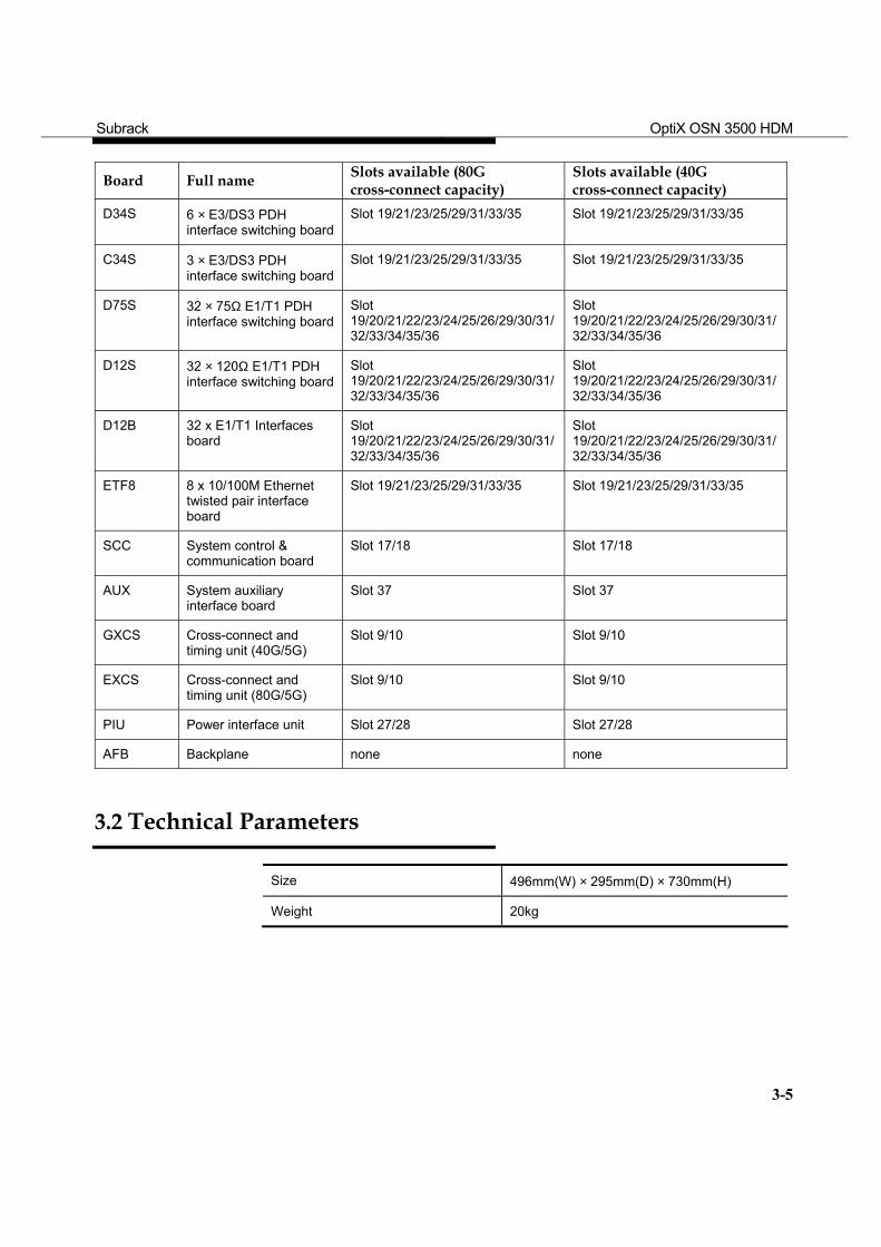
Board Full name Slots available (80G cross-connect capacity)
Slots available (40G cross-connect capacity)
SL64 STM-64 optical interface board
Slot 7/8/11/12 Slot 8/11
SL16 STM-16 optical interface board
Slot 5/6/7/8/11/12/13/14 Slot 6/7/8/11/12/13
SLQ4 4 × STM-4 optical interface board
Slot 5/6/7/8/11/12/13/14 Slot 6/7/8/11/12/13
SLD4 2 × STM-4 optical interface board
Slot 1/2/3/4/5/6/7/8/11/12/13/14/ 15/16/17
Slot 6/7/8/11/12/13
SL4 STM-4 optical interface board
Slot 1/2/3/4/5/6/7/8/11/12/13/14/ 15/16/17
Slot 1/2/3/4/5/6/7/8/11/12/13/14/ 15/16
SLQ1 4 × STM-1 optical interface board
Slot 1/2/3/4/5/6/7/8/11/12/13/14/ 15/16/17
Slot 1/2/3/4/5/6/7/8/11/12/13/14/ 15/16
SL1 STM-1 optical interface board
Slot 1/2/3/4/5/6/7/8/11/12/13/14/ 15/16/17
Slot 1/2/3/4/5/6/7/8/11/12/13/14/ 15/16
Subrack OptiX OSN 3500 HDM
3-4
Board Full name Slots available (80G cross-connect capacity)
Slots available (40G cross-connect capacity)
SEP1 STM-1 line processing board
Slot 1/2/3/4/5/6/13/14/15/16/17 Slot 1/2/3/4/5/6/13/14/ 15/16
BA2/ BPA
Optical booster amplifier board/Optical booster & pre-amplifier board
Slot 1/2/3/4/5/6/7/8/11/12/13/14/ 15/16/17
Slot 1/2/3/4/5/6/7/8/11/12/13/14/ 15/16/17
DCU Dispersion compensation board
Slot 1/2/3/4/5/6/7/8/11/12/13/14/ 15/16/17/18
Slot 1/2/3/4/5/6/7/8/11/12/13/14/ 15/16/17/18
SPQ4 4 × E4/STM-1 processing board
Slot 2/3/4/5/13/14/15/16 Slot 2/3/4/5/13/14/15/16
PD3 6 × E3/DS3 processing board
Slot 2/3/4/5/13/14/15/16 Slot 2/3/4/5/13/14/15/16
PL3 3 × E3/DS3 processing board
Slot 2/3/4/5/13/14/15/16 Slot 2/3/4/5/13/14/15/16
PQ1 63 × E1 processing board
Slot 1/2/3/4/5/13/14/15/16 Slot 1/2/3/4/5/13/14/15/16
PQM 63 × T1/E1 processing board
Slot 1/2/3/4/5/13/14/15/16 Slot 1/2/3/4/5/13/14/15/16
EGS2 2-port gigabit Ethernet optical interface board with Lanswitch
Slot 5/6/7/8/11/12/13/14 Slot 6/7/8/11/12/13
EFS0 Fast Ethernet interface board with Lanswitch
Slot 2/3/4/5/13/14/15/16 Slot 2/3/4/5/13/14/15/16
EFS4 4-port fast Ethernet interface board with Lanswitch
Slot 1/2/3/4/5/6/7/8/11/12/13/14/ 15/16/17
Slot 1/2/3/4/5/6/7/8/11/12/13/14/ 15/16
EU08 8 × STM-1 electrical interface board
Slot 19/21/23/25/29/31/33/35 Not support.
OU08 8 × STM-1 optical interface board
Slot 19/21/23/25/29/31/33/35 Not support.
EU04 4 × STM-1 electrical interface board
Slot 19/21/23/25/29/31/33/35 Slot 19/21/23/25/29/31/33/35
TSB8 8 × PDH interface switching & bridging board
Slot 19/20/35/36 Slot 19/20/35/36
TSB4 4 × PDH interface switching & bridging board
Slot 19/35 Slot 19/35
Subrack OptiX OSN 3500 HDM
3-5
Board Full name Slots available (80G cross-connect capacity)
Slots available (40G cross-connect capacity)
D34S 6 × E3/DS3 PDH interface switching board
Slot 19/21/23/25/29/31/33/35 Slot 19/21/23/25/29/31/33/35
C34S 3 × E3/DS3 PDH interface switching board
Slot 19/21/23/25/29/31/33/35 Slot 19/21/23/25/29/31/33/35
D75S 32 × 75Ω E1/T1 PDH interface switching board
Slot 19/20/21/22/23/24/25/26/29/30/31/32/33/34/35/36
Slot 19/20/21/22/23/24/25/26/29/30/31/32/33/34/35/36
D12S 32 × 120Ω E1/T1 PDH interface switching board
Slot 19/20/21/22/23/24/25/26/29/30/31/32/33/34/35/36
Slot 19/20/21/22/23/24/25/26/29/30/31/32/33/34/35/36
D12B 32 x E1/T1 Interfaces board
Slot 19/20/21/22/23/24/25/26/29/30/31/32/33/34/35/36
Slot 19/20/21/22/23/24/25/26/29/30/31/32/33/34/35/36
ETF8 8 x 10/100M Ethernet twisted pair interface board
Slot 19/21/23/25/29/31/33/35 Slot 19/21/23/25/29/31/33/35
SCC System control & communication board
Slot 17/18 Slot 17/18
AUX System auxiliary interface board
Slot 37 Slot 37
GXCS Cross-connect and timing unit (40G/5G)
Slot 9/10 Slot 9/10
EXCS Cross-connect and timing unit (80G/5G)
Slot 9/10 Slot 9/10
PIU Power interface unit Slot 27/28 Slot 27/28
AFB Backplane none none
3.2 Technical Parameters
Size 496mm(W) × 295mm(D) × 730mm(H)
Weight 20kg
OptiX OSN 3500 HDM
4-1
4 Boards
4.1 Classified Board Description
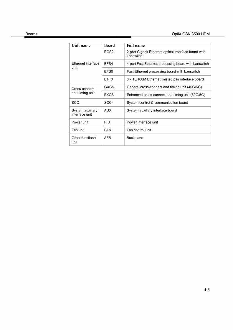
In terms of functions, boards can be classified into the following types: SDH interface unit PDH interface unit Ethernet interface unit Cross-connect unit SCC unit Auxiliary interface unit Power unit Fan unit Other functional unit
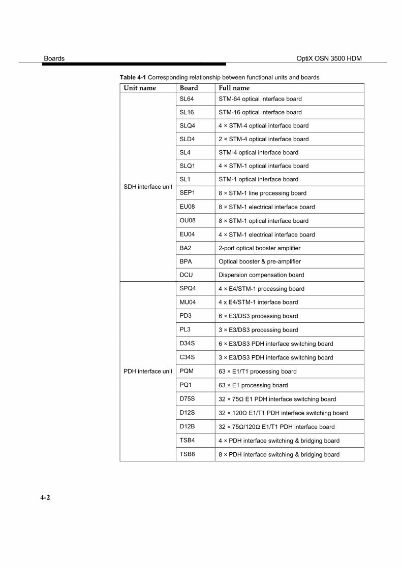
Table 4-1 shows the corresponding relationship between the functional units and boards.
Boards OptiX OSN 3500 HDM
4-2
Table 4-1 Corresponding relationship between functional units and boards
Unit name Board Full name SL64 STM-64 optical interface board
SL16 STM-16 optical interface board
SLQ4 4 × STM-4 optical interface board
SLD4 2 × STM-4 optical interface board
SL4 STM-4 optical interface board
SLQ1 4 × STM-1 optical interface board
SL1 STM-1 optical interface board
SEP1 8 × STM-1 line processing board
EU08 8 × STM-1 electrical interface board
OU08 8 × STM-1 optical interface board
EU04 4 × STM-1 electrical interface board
BA2 2-port optical booster amplifier
BPA Optical booster & pre-amplifier
SDH interface unit
DCU Dispersion compensation board
SPQ4 4 × E4/STM-1 processing board
MU04 4 x E4/STM-1 interface board
PD3 6 × E3/DS3 processing board
PL3 3 × E3/DS3 processing board
D34S 6 × E3/DS3 PDH interface switching board
C34S 3 × E3/DS3 PDH interface switching board
PQM 63 × E1/T1 processing board
PQ1 63 × E1 processing board
D75S 32 × 75Ω E1 PDH interface switching board
D12S 32 × 120Ω E1/T1 PDH interface switching board
D12B 32 × 75Ω/120Ω E1/T1 PDH interface board
TSB4 4 × PDH interface switching & bridging board
PDH interface unit
TSB8 8 × PDH interface switching & bridging board
Boards OptiX OSN 3500 HDM
4-3
Unit name Board Full name EGS2 2-port Gigabit Ethernet optical interface board with
Lanswitch
EFS4 4-port Fast Ethernet processing board with Lanswitch
EFS0 Fast Ethernet processing board with Lanswitch
Ethernet interface unit
ETF8 8 x 10/100M Ethernet twisted pair interface board
GXCS General cross-connect and timing unit (40G/5G) Cross-connect and timing unit EXCS Enhanced cross-connect and timing unit (80G/5G)
SCC SCC System control & communication board
System auxiliary interface unit
AUX System auxiliary interface board
Power unit PIU Power interface unit
Fan unit FAN Fan control unit
Other functional unit
AFB Backplane
Boards OptiX OSN 3500 HDM
4-4
4.2 Board Appearance
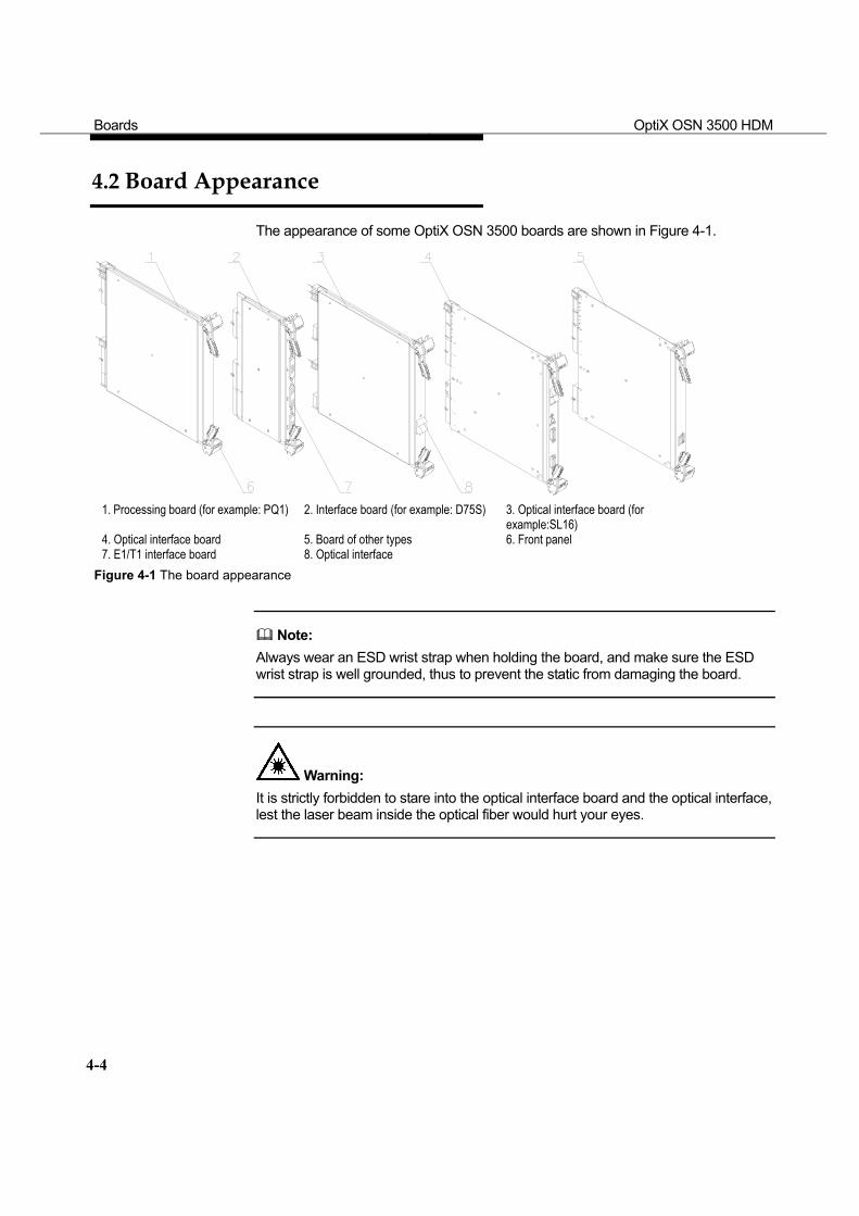
The appearance of some OptiX OSN 3500 boards are shown in Figure 4-1.
1. Processing board (for example: PQ1) 2. Interface board (for example: D75S) 3. Optical interface board (for
example:SL16) 4. Optical interface board 5. Board of other types 6. Front panel 7. E1/T1 interface board 8. Optical interface
Figure 4-1 The board appearance
Note: Always wear an ESD wrist strap when holding the board, and make sure the ESD wrist strap is well grounded, thus to prevent the static from damaging the board.
Warning: It is strictly forbidden to stare into the optical interface board and the optical interface, lest the laser beam inside the optical fiber would hurt your eyes.
Boards OptiX OSN 3500 HDM
4-5
4.3 SL64
SL64 is the 1 × STM-64 optical interface board, responsible for STM-64 optical signal processing. When the subrack cross-connect capacity is 80G, SL64 can be seated in Slot 7,8, 11 and 12 of the subrack; When the subrack cross-connect capacity is 40G, SL64 can be seated in Slot 8 and 11 of the subrack.
4.3.1 Functions and Principles
1. Functions
Receive/transmit one channel of STM-64 optical signal. Support STM-64-4C concatenated services. Support I-64.1, S-64.2b, L64.2b (used together with BA), Le-64.2, Ls-64 and
V-64.2b (used together with BA, PA and DCU) optical interface for different transmission distances.
Support fixed wavelength output, so that it can be connected with the multiplex unit of wavelength division multiplexing (WDM) equipment directly without the wavelength conversion unit.
Support various protection schemes such as two-fiber and four-fiber ring multiplex section protection (MSP), linear MSP and subnetwork connection protection (SNCP).
Support shared optical path protection of MSP ring and SNCP ring, and that of two MSP rings.
Provide abundant alarm and performance events for convenient equipment management and maintenance.
Support inloop and outloop at optical interfaces for fast fault location. Support automatic laser shutdown (ALS) function, avoiding laser injury to
human body during maintenance. Support on-line query of the board information and the optical power. Support configuration of such bytes as D1, D2 ~ D12, E1 and E2 to transparent
transmission or into other unused overhead bytes. Support smooth software upgrade and expansion.
2. Principles
Figure 4-1 shows the principle block diagram of SL64.

Boards OptiX OSN 3500 HDM
4-6
LAN
485
-48V
SCC
Standby cross-connect board
SDH signalprocessing
unit
Interfaceunit
Data andclock
recoveryunit
Active cross-connect board
Timing unitOverhead
processing unitControl and
communication unit
Overhead bus
Clock signal
Pow er module
Cross-connectand timing unit
1 x STM-64optical signal
Figure 4-1 Principle block diagram of SL64 The STM-64 optical signal is accessed at the interface unit and sent to the SDH signal processing unit after data and clock signal extraction at data and clock recovery unit. The SDH signal processing unit implements frame search, section overhead (SOH) termination and insertion, overhead byte extraction, pointer justification and path overhead (POH) monitoring to the incoming signal and then sends it to overhead processing unit for further processing. After that, the signal is re-timed with the system clock, and then multiplexed into 622M data signal after cross-connect and finally sent to the cross-connect and timing unit. The timing unit extracts the clock signal at line side and receives system clock and frame header from the active and standby cross-connect boards. It also provides clock signal for other modules on the board. The control and communication unit mainly functions control, communication, and service configuration of the board. The power module provides all modules of the board with DC power supply with required voltage. The overhead processing unit extracts the overhead bytes from the two channels of overhead signals it receives, and sends the extracted bytes to SCC and its paired board through the overhead bus according to related sequence and clock requirements. In transmit direction, the overhead processing unit re-arranges the received overhead signals from SCC or its paired board and then inserts them into the SOH.
Boards OptiX OSN 3500 HDM
4-7
4.3.2 Front Panel
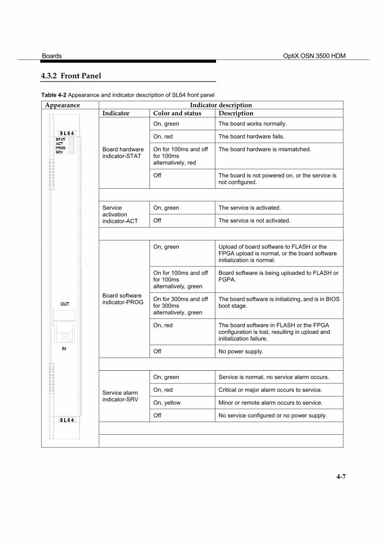
Table 4-2 Appearance and indicator description of SL64 front panel
Appearance Indicator description Indicator Color and status Description
On, green The board works normally.
On, red The board hardware fails.
On for 100ms and off for 100ms alternatively, red
The board hardware is mismatched. Board hardware indicator-STAT
Off The board is not powered on, or the service is not configured.
On, green The service is activated. Service activation indicator-ACT Off The service is not activated.
On, green Upload of board software to FLASH or the FPGA upload is normal, or the board software initialization is normal.
On for 100ms and off for 100ms alternatively, green
Board software is being uploaded to FLASH or FGPA.
On for 300ms and off for 300ms alternatively, green
The board software is initializing, and is in BIOS boot stage.
On, red The board software in FLASH or the FPGA configuration is lost, resulting in upload and initialization failure.
Board software indicator-PROG
Off No power supply.
On, green Service is normal, no service alarm occurs.
On, red Critical or major alarm occurs to service.
On, yellow Minor or remote alarm occurs to service.
Service alarm indicator-SRV
Off No service configured or no power supply.
Boards OptiX OSN 3500 HDM
4-8
4.3.3 Interface
The optical interface of SL64 is LC.
4.3.4 Board Configuration
Before using SL64 for running service, parameters should be set for it through transmission network management system (NM). Configuration should be provided to the following bytes for the line board:
J1 J1 is the path trace byte.Successive transmission of the higher order access point identifier through J1 at the transmit end helps the receive end learn that its connection with the specified transmit end is in continuous connection status. When J1 mismatch is detected at receive end, the corresponding VC-4 path will generate HP-TIM alarm.
C2 C2 is the signal label byte, indicating the multiplexing structure of VC-4 frame and the payload property. It is required that the C2 bytes transmitted match those received. Once mismatch is detected, the corresponding VC-4 path will generate HP-SLM alarm and insert all “1”s into the C4 in downstream stations.
4.3.5 Technical Parameters
Description Parameter SL64
Rate 9953280kbit/s
Processing capability
Process 1 × STM-64 standard service or concatenated service
Line code pattern
NRZ
Connector LC
Size (mm) 262.05 × 220 × 25.4
Weight (kg) 1.118
Power consumption (W)
32
Boards OptiX OSN 3500 HDM
4-9
Description Parameter SL64
Environment parameter (optional)
Long term operating condition Temperature: 0°C ~ 40°C Humidity:20% ~ 90% Short term operating condition Temperature: -5°C ~ 50°C Humidity:20% ~ 90% Environment for Storage Temperature: -40°C ~ +70°C Humidity:10% ~ 100% Environment for Transportation Temperature: -40°C ~ +70°C Humidity:10% ~ 100%
Optical module type
I-64.1 S-64.2b L-64.2b Le-64.2 Ls-64.2 V-64.2b(BA+PA+DCU)
Wavelength (nm)
1310 1550 1550 1550 1550 1550.12
Transmission distance (km)
0~2 2~40 30~70 30~70 80 70~120
Launched power (dBm)
-6 ~ -1 -1 ~ -2 / 1 ~ 4 3 ~ 5 /
Receiver sensitivity (dBm)
-14 -17 -17 -22.5 -24 -27
Boards OptiX OSN 3500 HDM
4-10
4.4 SL16
SL16 is the STM-16 optical interface board, responsible for STM-16 optical signal processing. When the subrack cross-connect capacity is 80G, SL16 can be seated in Slot 5 ~ 8 and 11 ~ 14 of the subrack; When the subrack cross-connect capacity is 40G, SL16 can be seated in Slot 6 ~ 8 and 11 ~ 13 of the subrack.
4.4.1 Functions and Principles
1. Functions
Receive/transmit one channel of STM-16 optical signal. Support VC-4-4C, VC-4-8C, and VC-4-16C concatenated services. Support I-16, S-16.1, L-16.1, L-16.2, L-16.2Je, V-16.2Je (used together with
BA) and U-16.2Je (used together with BA and PA) optical modules for different transmission distances.
Support fixed wavelength output, so that it can be connected with the multiplex unit of WDM equipment directly without using the wavelength conversion unit.
Support various protection schemes such as two-fiber and four-fiber bidirectional MSP, ring, linear MSP and SNCP.
Support shared optical path protection of MSP ring and SNCP ring, and that of two MSP rings.
Provide abundant alarm and performance events for convenient equipment management and maintenance.
Support inloop and outloop at optical interfaces for fast fault location. Support ALS function, avoiding laser injury to human body during
maintenance. Support on-line query of the board information and the optical power. Support configuration of such bytes as D1, D2 ~ D12, E1 and E2 to transparent
transmission or into other unused overhead bytes. Support smooth software upgrade and expansion.
2. Principles
Figure 4-2 shows the principle block diagram of SL16.
Boards OptiX OSN 3500 HDM
4-11
LAN
485
-48V
SCC
Standby cross-connect board
SDH signalprocessing
unit
Interfaceunit
Data andclock
recoveryunit
Active cross-connect board
Timing unitOverhead
processing unitControl and
communication unit
Overhead bus
Clock signal
Pow er module
Cross-connectand timing unit
1 x STM-16optical signal
Figure 4-2 Principle block diagram of SL16 The STM-16 optical signal is accessed at the interface unit and sent to the SDH signal processing unit after data and clock signal extraction at data and clock recovery unit. The SDH signal processing unit implements frame search, SOH termination and insertion, overhead byte extraction, pointer justification and POH monitoring to the incoming signals and then sends them to overhead processing unit for further processing. After that, the signals are re-timed with the system clock, and then multiplexed into 622M data signals after cross-connect and finally sent to the cross-connect and timing unit. The timing unit extracts the clock signal at line side and receives system clock and frame header from the active and standby cross-connect boards. It also provides clock signal for other modules on the board. The control and communication unit mainly functions control, communication and service configuration of the board. The power module provides all modules of the board with DC power supply with required voltage. The overhead processing unit extracts the overhead bytes from the one channel of overhead signal it receives, and sends the extracted bytes to SCC and its paired board through the overhead bus according to related sequence and clock requirements. In transmit direction, the overhead processing unit re-arranges the received overhead signals from SCC or its paired board and then inserts them into the SOH.
Boards OptiX OSN 3500 HDM
4-12
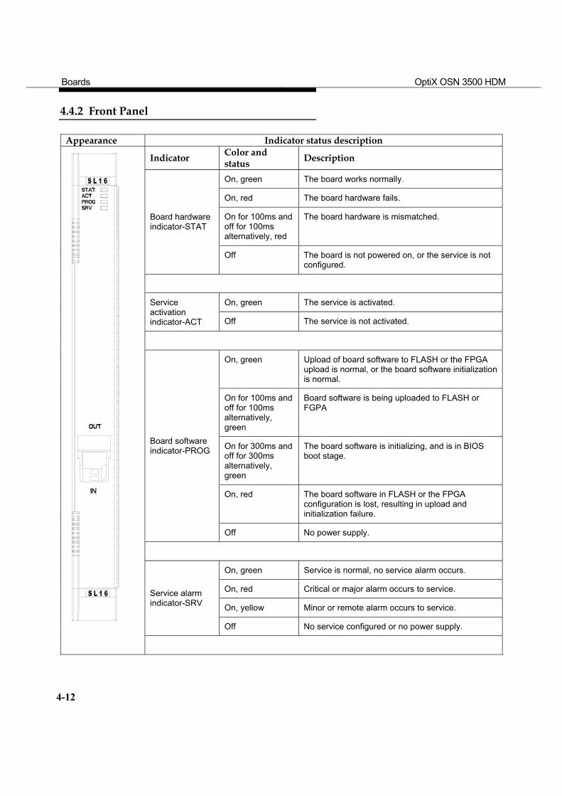
4.4.2 Front Panel
Appearance Indicator status description
Indicator Color and status Description
On, green The board works normally.
On, red The board hardware fails.
On for 100ms and off for 100ms alternatively, red
The board hardware is mismatched. Board hardware indicator-STAT
Off The board is not powered on, or the service is not configured.
On, green The service is activated. Service activation indicator-ACT Off The service is not activated.
On, green Upload of board software to FLASH or the FPGA upload is normal, or the board software initialization is normal.
On for 100ms and off for 100ms alternatively, green
Board software is being uploaded to FLASH or FGPA
On for 300ms and off for 300ms alternatively, green
The board software is initializing, and is in BIOS boot stage.
On, red The board software in FLASH or the FPGA configuration is lost, resulting in upload and initialization failure.
Board software indicator-PROG
Off No power supply.
On, green Service is normal, no service alarm occurs.
On, red Critical or major alarm occurs to service.
On, yellow Minor or remote alarm occurs to service. Service alarm indicator-SRV
Off No service configured or no power supply.
Boards OptiX OSN 3500 HDM
4-13
4.4.3 Interface
The optical interface of SL16 is LC.
4.4.4 Board Configuration
Before using SL16 for running service, parameters should be set for it through NM. Configuration should be provided to the following bytes for the line board:
J1 J1 is the path trace byte.Successive transmission of the higher order access point identifier through J1 at the transmit end helps the receive end learn that its connection with the specified transmit end is in continuous connection status. When J1 mismatch is detected at receive end, the corresponding VC-4 path will generate HP-TIM alarm.
C2 C2 is the signal label byte, indicating the multiplexing structure of VC-4 frame and the payload property. It is required that the C2 bytes transmitted match those received. Once mismatch is detected, the corresponding VC-4 path will generate HP-SLM alarm and insert all “1”s into the C4 in downstream stations.
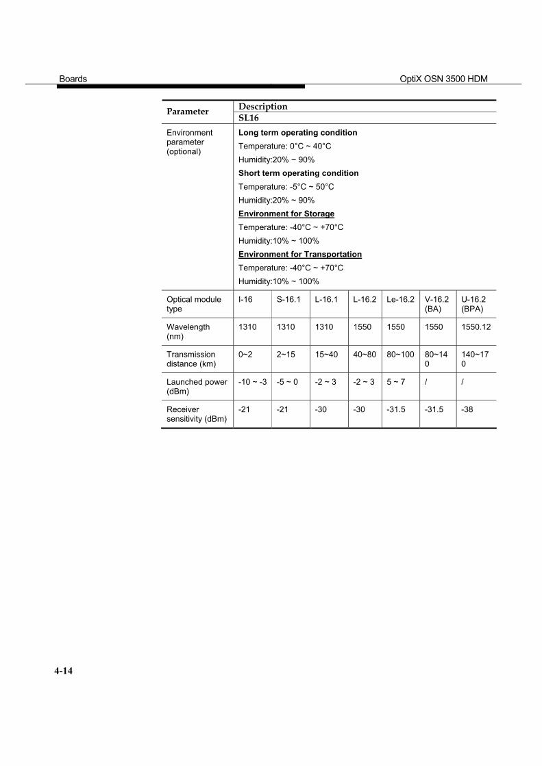
4.4.5 Technical Parameters
Description Parameter SL16
Rate 2488320kbit/s
Processing capability
Process 1 × STM-16 standard service or concatenated service
Line code pattern
NRZ
Connector LC
Size (mm) 262.05 × 220 × 25.4
Weight (kg) 1.100
Power consumption (W)
20
Boards OptiX OSN 3500 HDM
4-14
Description Parameter SL16
Environment parameter (optional)
Long term operating condition Temperature: 0°C ~ 40°C Humidity:20% ~ 90% Short term operating condition Temperature: -5°C ~ 50°C Humidity:20% ~ 90% Environment for Storage Temperature: -40°C ~ +70°C Humidity:10% ~ 100% Environment for Transportation Temperature: -40°C ~ +70°C Humidity:10% ~ 100%
Optical module type
I-16 S-16.1 L-16.1 L-16.2 Le-16.2 V-16.2 (BA)
U-16.2 (BPA)
Wavelength (nm)
1310 1310 1310 1550 1550 1550 1550.12
Transmission distance (km)
0~2 2~15 15~40 40~80 80~100 80~140
140~170
Launched power (dBm)
-10 ~ -3 -5 ~ 0 -2 ~ 3 -2 ~ 3 5 ~ 7 / /
Receiver sensitivity (dBm)
-21 -21 -30 -30 -31.5 -31.5 -38
Boards OptiX OSN 3500 HDM
4-15
4.5 SLQ4/SLD4/SL4
SLQ4 is the 4 × STM-4 optical interface board; SLD4 is the 2 × STM-4 optical interface board; and SL4 is the 1 × STM-4 optical interface board. All are responsible for STM-4 optical signal processing. Table 4-3 shows the difference between these three optical interface boards. Table 4-3 Comparison between SLQ4, SLD4 and SL4
Comparison SL4 SLD4 SLQ4 Processing capability
1 × STM-4 2 × STM-4 4 × STM-4
Slot available (Cross-connect capacity is 80G)
Slot 1 ~ 8, 11 ~ 17 Slot 1 ~ 8, 11 ~ 17 Slot 5 ~ 8, 11 ~ 14
Slot available (Cross-connect capacity is 40G)
Slot 1 ~ 8, 11 ~ 16 Slot 6 ~ 8, 11 ~ 13 Slot 6 ~ 8, 11 ~ 13
4.5.1 Functions and Principles
1. Functions
SLQ4, SLD4 and SL4 can access and process 4, 2 and 1 × STM-4 optical signal respectively.
Support VC-4-4C concatenated services. Support I-4, S-4.1, L-4.1, L-4.2 and Ve-4.2 optical interfaces for different
transmission distances. Support various protection schemes such as two-fiber and four-fiber
bidirectional MSP, linear MSP, and SNCP. Provide abundant alarm and performance events for convenient equipment
management and maintenance. Support inloop and outloop at optical interfaces for fast fault location. Support ALS function, avoiding laser injury to human body during
maintenance. Support on-line query of the board information. Support configuration of such bytes as D1, D2 ~ D12, E1 and E2 to transparent
transmission or into other unused overhead bytes. Support smooth software upgrade and expansion.
2. Principles
Figure 4-3 shows the principle block diagram of SLQ4/SLD4/SL4.
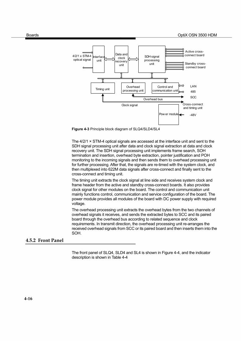
Boards OptiX OSN 3500 HDM
4-16
LAN
485
-48V
SCC
Standby cross-connect board
SDH signalprocessing
unit
Interfaceunit
Data andclock
recoveryunit
Active cross-connect board
Timing unitOverhead
processing unitControl and
communication unit
Overhead bus
Clock signal
Pow er module
Cross-connectand timing unit
4/2/1 x STM-4optical signal
Figure 4-3 Principle block diagram of SLQ4/SLD4/SL4 The 4/2/1 × STM-4 optical signals are accessed at the interface unit and sent to the SDH signal processing unit after data and clock signal extraction at data and clock recovery unit. The SDH signal processing unit implements frame search, SOH termination and insertion, overhead byte extraction, pointer justification and POH monitoring to the incoming signals and then sends them to overhead processing unit for further processing. After that, the signals are re-timed with the system clock, and then multiplexed into 622M data signals after cross-connect and finally sent to the cross-connect and timing unit. The timing unit extracts the clock signal at line side and receives system clock and frame header from the active and standby cross-connect boards. It also provides clock signal for other modules on the board. The control and communication unit mainly functions control, communication and service configuration of the board. The power module provides all modules of the board with DC power supply with required voltage. The overhead processing unit extracts the overhead bytes from the two channels of overhead signals it receives, and sends the extracted bytes to SCC and its paired board through the overhead bus according to related sequence and clock requirements. In transmit direction, the overhead processing unit re-arranges the received overhead signals from SCC or its paired board and then inserts them into the SOH.
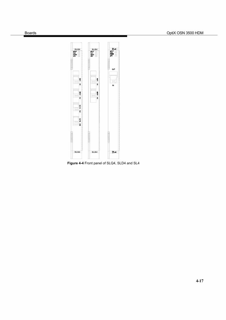
4.5.2 Front Panel
The front panel of SLQ4, SLD4 and SL4 is shown in Figure 4-4, and the indicator description is shown in Table 4-4
Boards OptiX OSN 3500 HDM
4-17
Figure 4-4 Front panel of SLQ4, SLD4 and SL4
Boards OptiX OSN 3500 HDM
4-18
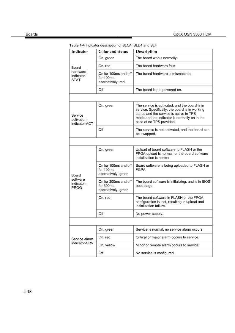
Table 4-4 Indicator description of SLQ4, SLD4 and SL4
Indicator Color and status Description On, green The board works normally.
On, red The board hardware fails.
On for 100ms and off for 100ms alternatively, red
The board hardware is mismatched.
Board hardware indicator- STAT
Off The board is not powered on.
On, green The service is activated, and the board is in service. Specifically, the board is in working status and the service is active in TPS mode;and the indicator is normally on in the case of no TPS provided.
Service activation indicator-ACT
Off The service is not activated, and the board can be swapped.
On, green Upload of board software to FLASH or the FPGA upload is normal, or the board software initialization is normal.
On for 100ms and off for 100ms alternatively, green
Board software is being uploaded to FLASH or FGPA
On for 300ms and off for 300ms alternatively, green
The board software is initializing, and is in BIOS boot stage.
On, red The board software in FLASH or the FPGA configuration is lost, resulting in upload and initialization failure.
Board software indicator- PROG
Off No power supply.
On, green Service is normal, no service alarm occurs.
On, red Critical or major alarm occurs to service.
On, yellow Minor or remote alarm occurs to service.
Service alarm indicator-SRV
Off No service is configured.
Boards OptiX OSN 3500 HDM
4-19
4.5.3 Interface
SLQ4, SLD4 and SL4 provide LC optical interfaces.
4.5.4 Board Configuration
Before using SLQ4, SLD4 and SL4 for running service, parameters should be set for it through NM. Configuration should be provided to the following bytes for the line board:
J1 J1 is the path trace byte.Successive transmission of the higher order access point identifier through J1 at the transmit end helps the receive end learn that its connection with the specified transmit end is in continuous connection status. When J1 mismatch is detected at receive end, the corresponding VC-4 path will generate HP-TIM alarm.
C2 C2 is the signal label byte, indicating the multiplexing structure of VC-4 frame and the payload property. It is required that the C2 bytes transmitted match those received. Once mismatch is detected, the corresponding VC-4 path will generate HP-SLM alarm and insert all “1”s into the C4 in downstream stations.
4.5.5 Technical Parameters
Description Parameter SLQ4 SLD4 SL4
Rate 622080kbit/s
Processing capability
4 × STM-4 2 × STM-4 1 × STM-4
Line code pattern
NRZ
Connector LC
Size (mm) 262.05 × 220 × 25.4
Weight (kg) 1.036 1.032 1.030
Power consumption (W)
16 15 14.5
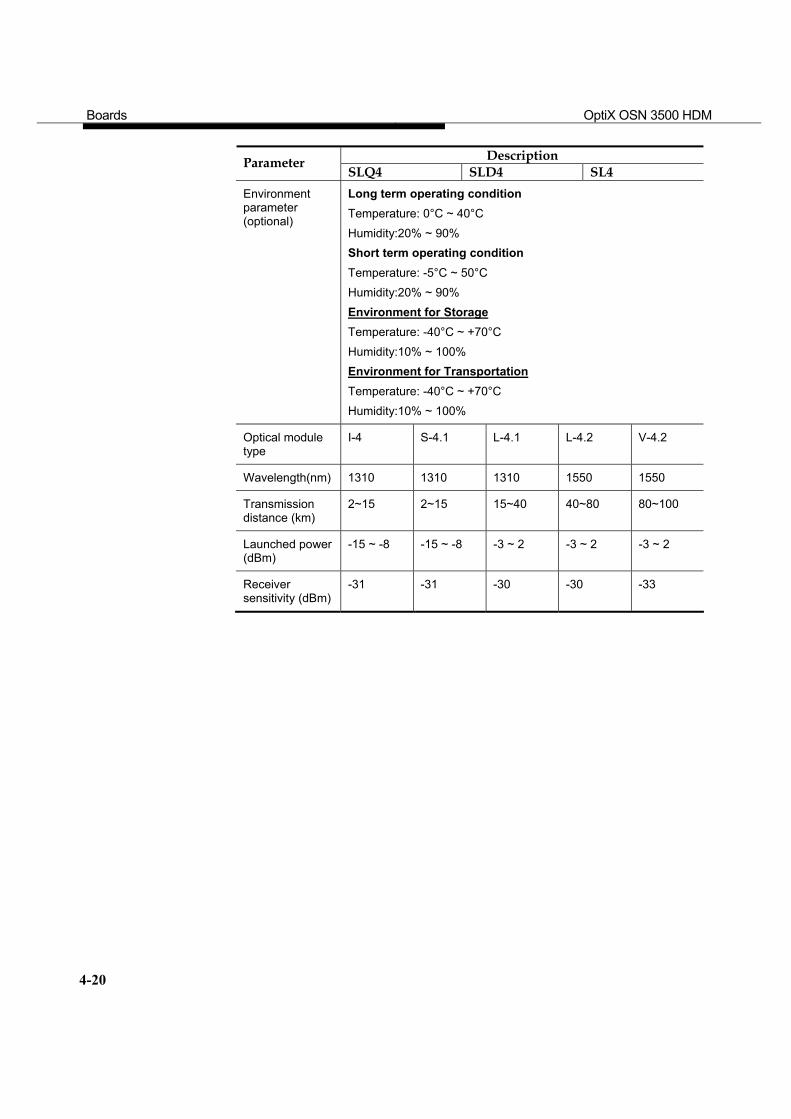
Boards OptiX OSN 3500 HDM
4-20
Description Parameter SLQ4 SLD4 SL4
Environment parameter (optional)
Long term operating condition Temperature: 0°C ~ 40°C Humidity:20% ~ 90% Short term operating condition Temperature: -5°C ~ 50°C Humidity:20% ~ 90% Environment for Storage Temperature: -40°C ~ +70°C Humidity:10% ~ 100% Environment for Transportation Temperature: -40°C ~ +70°C Humidity:10% ~ 100%
Optical module type
I-4 S-4.1 L-4.1 L-4.2 V-4.2
Wavelength(nm) 1310 1310 1310 1550 1550
Transmission distance (km)
2~15 2~15 15~40 40~80 80~100
Launched power (dBm)
-15 ~ -8 -15 ~ -8 -3 ~ 2 -3 ~ 2 -3 ~ 2
Receiver sensitivity (dBm)
-31 -31 -30 -30 -33
Boards OptiX OSN 3500 HDM
4-21
4.6 SLQ1/SL1
SLQ1 is the 4 × STM-1 optical interface board; and SL1 is the 1 × STM-1 optical interface board. Both are responsible for STM-1 optical signal processing board. Table 4-5 shows the difference between these two optical interface boards. Table 4-5 Comparison between SLQ1 and SL1
Comparison SL1 SLQ1 Processing capability 1 × STM-1 4 × STM-1
Slot available (Cross-connect capacity is 80G)
Slot 1 ~ 8 and 11 ~ 17 Slot 1 ~ 8 and 11 ~ 17
Slot available (Cross-connect capacity is 40G)
Slot 1 ~ 8 and 11 ~ 16 Slot 1 ~ 8 and 11 ~ 16
4.6.1 Functions and Principles
1. Functions
SLQ1 and SL1 access and process four and one channel of STM-1 optical signal respectively.
Support Ie-1, I-1, S-1.1, L-1.1, L-1.2 and V-1.2 optical interfaces for different transmission distances.
Support various protection schemes such as two-fiber unidirectional MSP, linear MSP and SNCP.
Provide abundant alarm and performance events for convenient equipment management and maintenance.
Support inloop and outloop at optical interfaces for fast fault location. Support ALS function, avoiding laser injury to human body during
maintenance. Support on-line query of the board information. Support configuration of such bytes as D1, D2 ~ D12, E1 and E2 to transparent
transmission or into other unused overhead bytes. Support smooth software upgrade and expansion.
2. Principles
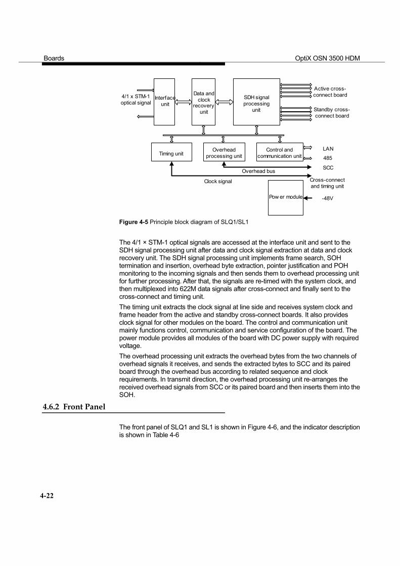
Figure 4-5 shows the principle block diagram of SLQ1/SL1.
Boards OptiX OSN 3500 HDM
4-22
LAN
485
-48V
SCC
Standby cross-connect board
SDH signalprocessing
unit
Interfaceunit
Data andclock
recoveryunit
Active cross-connect board
Timing unitOverhead
processing unitControl and
communication unit
Overhead bus
Clock signal
Pow er module
Cross-connectand timing unit
4/1 x STM-1optical signal
Figure 4-5 Principle block diagram of SLQ1/SL1 The 4/1 × STM-1 optical signals are accessed at the interface unit and sent to the SDH signal processing unit after data and clock signal extraction at data and clock recovery unit. The SDH signal processing unit implements frame search, SOH termination and insertion, overhead byte extraction, pointer justification and POH monitoring to the incoming signals and then sends them to overhead processing unit for further processing. After that, the signals are re-timed with the system clock, and then multiplexed into 622M data signals after cross-connect and finally sent to the cross-connect and timing unit. The timing unit extracts the clock signal at line side and receives system clock and frame header from the active and standby cross-connect boards. It also provides clock signal for other modules on the board. The control and communication unit mainly functions control, communication and service configuration of the board. The power module provides all modules of the board with DC power supply with required voltage. The overhead processing unit extracts the overhead bytes from the two channels of overhead signals it receives, and sends the extracted bytes to SCC and its paired board through the overhead bus according to related sequence and clock requirements. In transmit direction, the overhead processing unit re-arranges the received overhead signals from SCC or its paired board and then inserts them into the SOH.
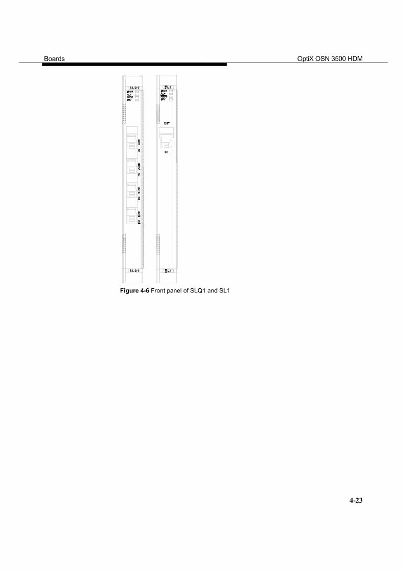
4.6.2 Front Panel
The front panel of SLQ1 and SL1 is shown in Figure 4-6, and the indicator description is shown in Table 4-6
Boards OptiX OSN 3500 HDM
4-23
Figure 4-6 Front panel of SLQ1 and SL1
Boards OptiX OSN 3500 HDM
4-24
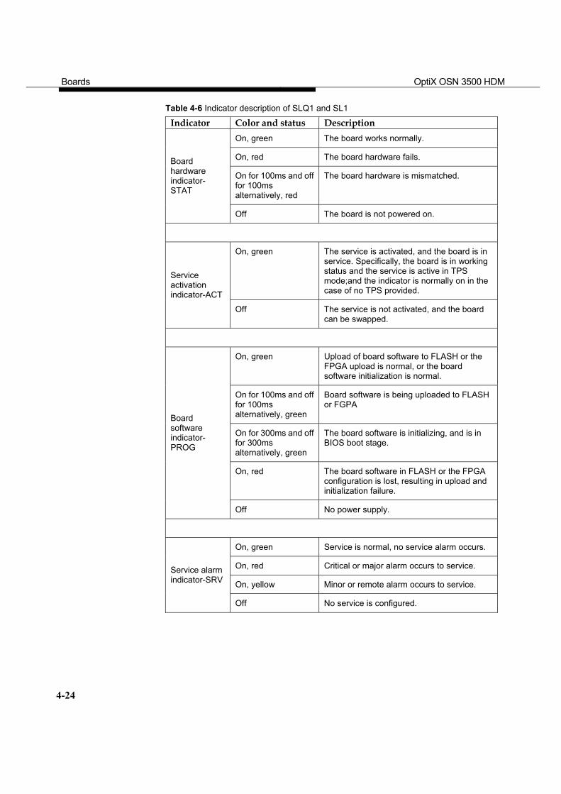
Table 4-6 Indicator description of SLQ1 and SL1
Indicator Color and status Description On, green The board works normally.
On, red The board hardware fails.
On for 100ms and off for 100ms alternatively, red
The board hardware is mismatched.
Board hardware indicator- STAT
Off The board is not powered on.
On, green The service is activated, and the board is in service. Specifically, the board is in working status and the service is active in TPS mode;and the indicator is normally on in the case of no TPS provided.
Service activation indicator-ACT
Off The service is not activated, and the board can be swapped.
On, green Upload of board software to FLASH or the FPGA upload is normal, or the board software initialization is normal.
On for 100ms and off for 100ms alternatively, green
Board software is being uploaded to FLASH or FGPA
On for 300ms and off for 300ms alternatively, green
The board software is initializing, and is in BIOS boot stage.
On, red The board software in FLASH or the FPGA configuration is lost, resulting in upload and initialization failure.
Board software indicator- PROG
Off No power supply.
On, green Service is normal, no service alarm occurs.
On, red Critical or major alarm occurs to service.
On, yellow Minor or remote alarm occurs to service.
Service alarm indicator-SRV
Off No service is configured.
Boards OptiX OSN 3500 HDM
4-25
4.6.3 Interface
The interface of SLQ1 and SL1 is LC.
4.6.4 Board Configuration
Before using SL1 for running service, parameters should be set for it through NM. Configuration should be provided to the following bytes for the line board:
J1 J1 is the path trace byte.Successive transmission of the higher order access point identifier through J1 at the transmit end helps the receive end learn that its connection with the specified transmit end is in continuous connection status. When J1 mismatch is detected at receive end, the corresponding VC-4 path will generate HP-TIM alarm.
C2 C2 is the signal label byte, indicating the multiplexing structure of VC-4 frame and the payload property. It is required that the C2 bytes transmitted match those received. Once mismatch is detected, the corresponding VC-4 path will generate HP-SLM alarm and insert all “1”s into the C4 in downstream stations.
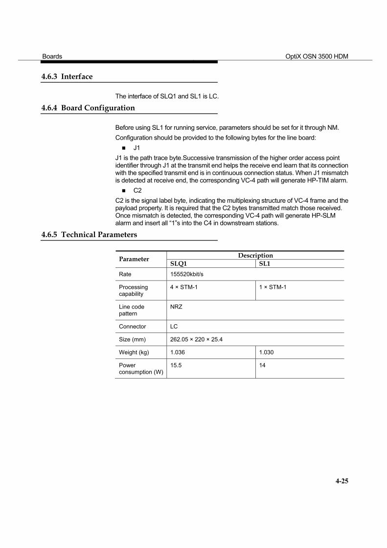
4.6.5 Technical Parameters
Description Parameter SLQ1 SL1
Rate 155520kbit/s
Processing capability
4 × STM-1 1 × STM-1
Line code pattern
NRZ
Connector LC
Size (mm) 262.05 × 220 × 25.4
Weight (kg) 1.036 1.030
Power consumption (W)
15.5 14
Boards OptiX OSN 3500 HDM
4-26
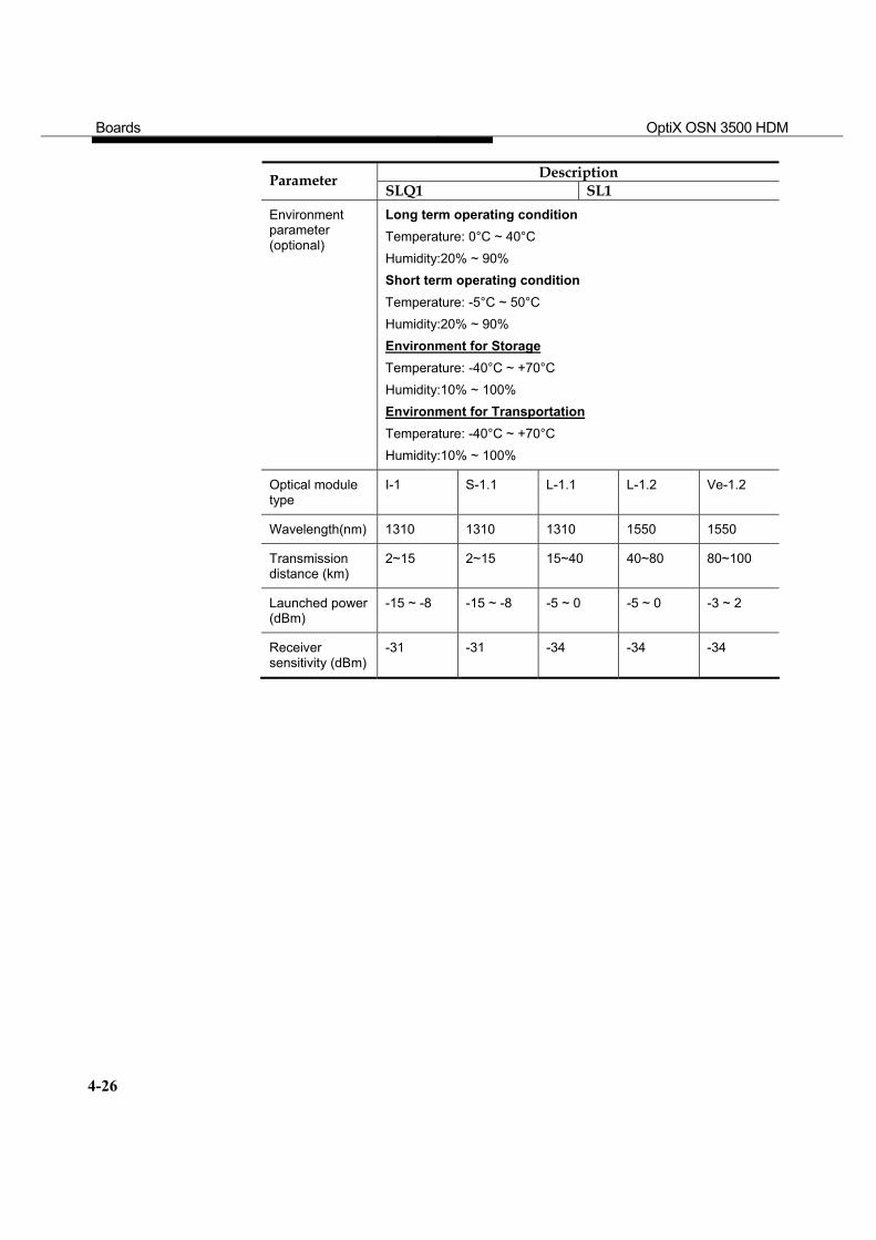
Description Parameter SLQ1 SL1
Environment parameter (optional)
Long term operating condition Temperature: 0°C ~ 40°C Humidity:20% ~ 90% Short term operating condition Temperature: -5°C ~ 50°C Humidity:20% ~ 90% Environment for Storage Temperature: -40°C ~ +70°C Humidity:10% ~ 100% Environment for Transportation Temperature: -40°C ~ +70°C Humidity:10% ~ 100%
Optical module type
I-1 S-1.1 L-1.1 L-1.2 Ve-1.2
Wavelength(nm) 1310 1310 1310 1550 1550
Transmission distance (km)
2~15 2~15 15~40 40~80 80~100
Launched power (dBm)
-15 ~ -8 -15 ~ -8 -5 ~ 0 -5 ~ 0 -3 ~ 2
Receiver sensitivity (dBm)
-31 -31 -34 -34 -34
Boards OptiX OSN 3500 HDM
4-27
4.7 SEP1/EU08/OU08/EU04/TSB8/
TSB4
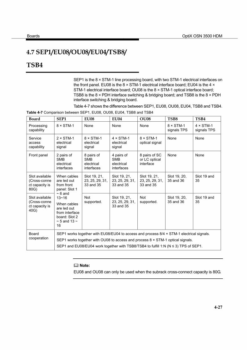
SEP1 is the 8 × STM-1 line processing board, with two STM-1 electrical interfaces on the front panel. EU08 is the 8 × STM-1 electrical interface board; EU04 is the 4 × STM-1 electrical interface board; OU08 is the 8 × STM-1 optical interface board; TSB8 is the 8 × PDH interface switching & bridging board; and TSB8 is the 8 × PDH interface switching & bridging board. Table 4-7 shows the difference between SEP1, EU08, OU08, EU04, TSB8 and TSB4.
Table 4-7 Comparison between SEP1, EU08, OU08, EU04, TSB8 and TSB4
Board SEP1 EU08 EU04 OU08 TSB8 TSB4 Processing capability
8 × STM-1 None None None 8 × STM-1 signals TPS
4 × STM-1 signals TPS
Service access capability
2 × STM-1 electrical signal
8 × STM-1 electrical signal
4 × STM-1 electrical signal
8 × STM-1 optical signal
None None
Front panel 2 pairs of SMB electrical interfaces
8 pairs of SMB electrical interfaces
4 pairs of SMB electrical interfaces
8 pairs of SC or LC optical interface
None None
Slot available (Cross-connect capacity is 80G)
Slot 19, 21, 23, 25, 29, 31, 33 and 35
Slot 19, 21, 23, 25, 29, 31, 33 and 35
Slot 19, 21, 23, 25, 29, 31, 33 and 35
Slot 19, 20, 35 and 36
Slot 19 and 35
Slot available (Cross-connect capacity is 40G)
When cables are led out from front panel: Slot 1 ~ 6 and 13~16 When cables are led out from interface board: Slot 2 ~ 5 and 13 ~ 16
Not supported.
Slot 19, 21, 23, 25, 29, 31, 33 and 35
Not supported.
Slot 19, 20, 35 and 36
Slot 19 and 35
Board cooperation
SEP1 works together with EU08/EU04 to access and process 8/4 × STM-1 electrical signals. SEP1 works together with OU08 to access and process 8 × STM-1 optical signals. SEP1 and EU08/EU04 work together with TSB8/TSB4 to fulfill 1:N (N ≤ 3) TPS of SEP1.
Note: EU08 and OU08 can only be used when the subrack cross-connect capacity is 80G.

Boards OptiX OSN 3500 HDM
4-28
4.7.1 Functions and Principles
1. Functions
SEP1 can process 8 × STM-1 services. EU08 provides 75Ω SMB unbalanced interface. OU08 supports I-1 and S-1.1 optical modules for different transmission
distances. Support various protection schemes such as linear MSP, MSP and SNCP. Provide abundant alarm and performance events for convenient equipment
management and maintenance. Support inloop and outloop at interfaces for fast fault location. Support ALS function, avoiding laser injury to human body during
maintenance. Support on-line query of the board information. Support configuration of such bytes as D1, D2 ~ D12, E1 and E2 to transparent
transmission or into other unused overhead bytes. Support smooth software upgrade and expansion.
2. Principles
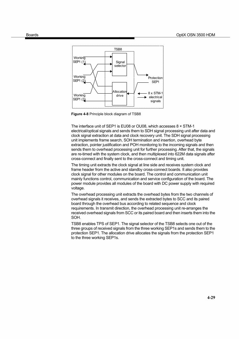
The principle block diagram of SEP1 and TSB8 is shown in Figure 4-7 and Figure 4-8 respectively.
LAN
485
-48V
SCC
Standby cross-connect board
SDH signalprocessing
unit
Interfaceunit
Data andclock
recoveryunit
Active cross-connect board
Timing unitOverhead
processing unitControl and
communication unit
Overhead bus
Clock signal
Pow er module
Cross-connectand timing unit
2/4/8 x STM-1optical/electrical
signals
Figure 4-7 Principle block diagram of SEP1
Boards OptiX OSN 3500 HDM
4-29
TSB8
Signalselector
WorkingSEP1 (1)
WorkingSEP1 (2)
WorkingSEP1 (3)
ProtectionSEP1
8 x STM-1electricalsignals
Allocationdrive
Figure 4-8 Principle block diagram of TSB8 The interface unit of SEP1 is EU08 or OU08, which accesses 8 × STM-1 electrical/optical signals and sends them to SDH signal processing unit after data and clock signal extraction at data and clock recovery unit. The SDH signal processing unit implements frame search, SOH termination and insertion, overhead byte extraction, pointer justification and POH monitoring to the incoming signals and then sends them to overhead processing unit for further processing. After that, the signals are re-timed with the system clock, and then multiplexed into 622M data signals after cross-connect and finally sent to the cross-connect and timing unit. The timing unit extracts the clock signal at line side and receives system clock and frame header from the active and standby cross-connect boards. It also provides clock signal for other modules on the board. The control and communication unit mainly functions control, communication and service configuration of the board. The power module provides all modules of the board with DC power supply with required voltage. The overhead processing unit extracts the overhead bytes from the two channels of overhead signals it receives, and sends the extracted bytes to SCC and its paired board through the overhead bus according to related sequence and clock requirements. In transmit direction, the overhead processing unit re-arranges the received overhead signals from SCC or its paired board and then inserts them into the SOH. TSB8 enables TPS of SEP1. The signal selector of the TSB8 selects one out of the three groups of received signals from the three working SEP1s and sends them to the protection SEP1. The allocation drive allocates the signals from the protection SEP1 to the three working SEP1s.
Boards OptiX OSN 3500 HDM
4-30
4.7.2 Front Panel
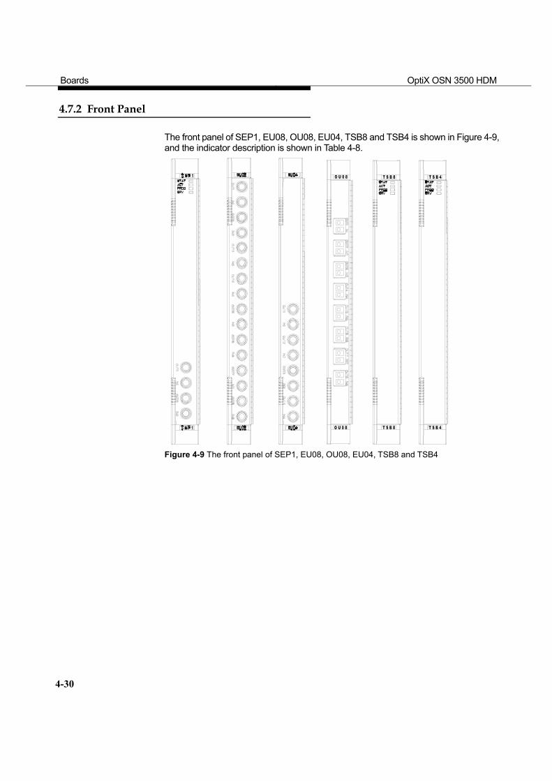
The front panel of SEP1, EU08, OU08, EU04, TSB8 and TSB4 is shown in Figure 4-9, and the indicator description is shown in Table 4-8.
Figure 4-9 The front panel of SEP1, EU08, OU08, EU04, TSB8 and TSB4
Boards OptiX OSN 3500 HDM
4-31
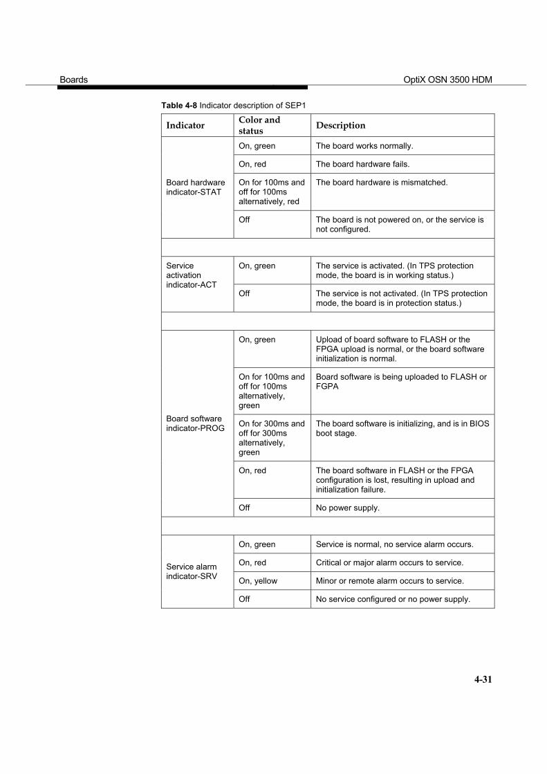
Table 4-8 Indicator description of SEP1
Indicator Color and status Description
On, green The board works normally.
On, red The board hardware fails.
On for 100ms and off for 100ms alternatively, red
The board hardware is mismatched. Board hardware indicator-STAT
Off The board is not powered on, or the service is not configured.
On, green The service is activated. (In TPS protection mode, the board is in working status.)
Service activation indicator-ACT
Off The service is not activated. (In TPS protection mode, the board is in protection status.)
On, green Upload of board software to FLASH or the FPGA upload is normal, or the board software initialization is normal.
On for 100ms and off for 100ms alternatively, green
Board software is being uploaded to FLASH or FGPA
On for 300ms and off for 300ms alternatively, green
The board software is initializing, and is in BIOS boot stage.
On, red The board software in FLASH or the FPGA configuration is lost, resulting in upload and initialization failure.
Board software indicator-PROG
Off No power supply.
On, green Service is normal, no service alarm occurs.
On, red Critical or major alarm occurs to service.
On, yellow Minor or remote alarm occurs to service.
Service alarm indicator-SRV
Off No service configured or no power supply.
Boards OptiX OSN 3500 HDM
4-32
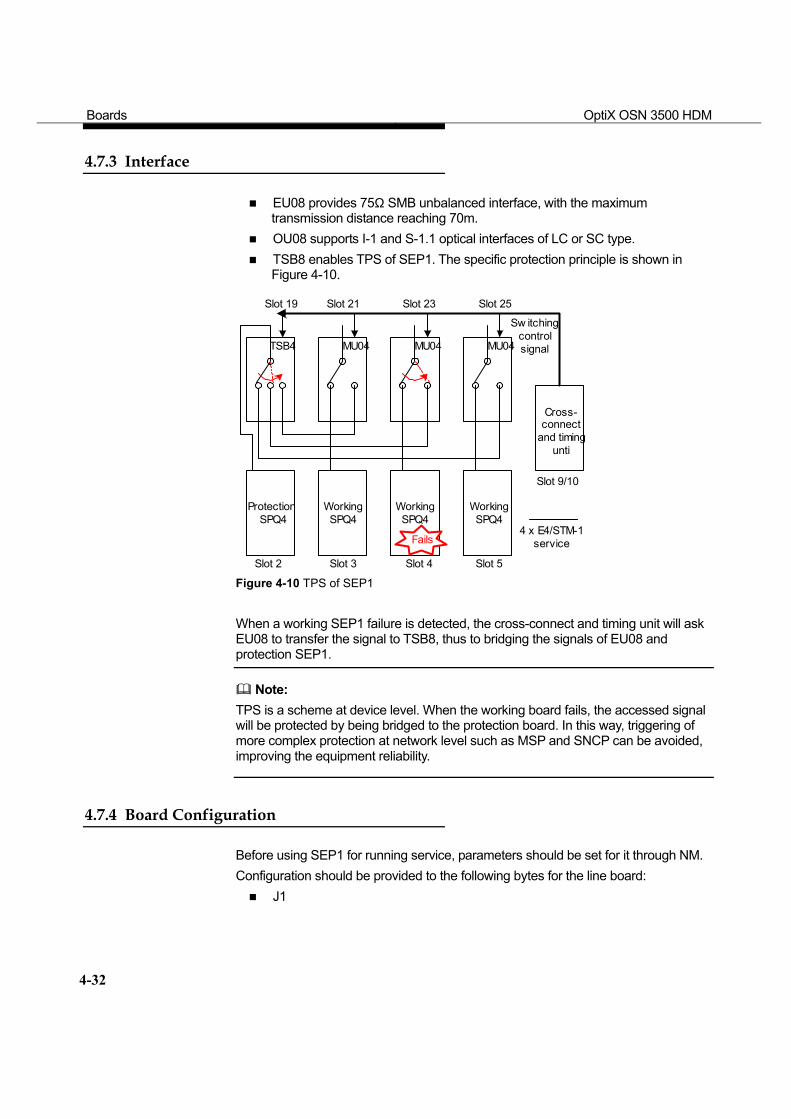
4.7.3 Interface
EU08 provides 75Ω SMB unbalanced interface, with the maximum transmission distance reaching 70m.
OU08 supports I-1 and S-1.1 optical interfaces of LC or SC type. TSB8 enables TPS of SEP1. The specific protection principle is shown in
Figure 4-10.
TSB4 MU04 MU04 MU04
Slot 21
ProtectionSPQ4
Slot 23 Slot 25Slot 19
Fails
WorkingSPQ4
WorkingSPQ4
WorkingSPQ4
Cross-connect
and timingunti
Sw itchingcontrolsignal
4 x E4/STM-1service
Slot 2
Slot 9/10
Slot 3 Slot 4 Slot 5 Figure 4-10 TPS of SEP1 When a working SEP1 failure is detected, the cross-connect and timing unit will ask EU08 to transfer the signal to TSB8, thus to bridging the signals of EU08 and protection SEP1.
Note: TPS is a scheme at device level. When the working board fails, the accessed signal will be protected by being bridged to the protection board. In this way, triggering of more complex protection at network level such as MSP and SNCP can be avoided, improving the equipment reliability.
4.7.4 Board Configuration
Before using SEP1 for running service, parameters should be set for it through NM. Configuration should be provided to the following bytes for the line board:
J1
Boards OptiX OSN 3500 HDM
4-33
J1 is the path trace byte.Successive transmission of the higher order access point identifier through J1 at the transmit end helps the receive end learn that its connection with the specified transmit end is in continuous connection status. When J1 mismatch is detected at receive end, the corresponding VC-4 path will generate HP-TIM alarm.
C2 C2 is the signal label byte, indicating the multiplexing structure of VC-4 frame and the payload property. It is required that the C2 bytes transmitted match those received. Once mismatch is detected, the corresponding VC-4 path will generate HP-SLM alarm and insert all “1”s into the C4 in downstream stations.
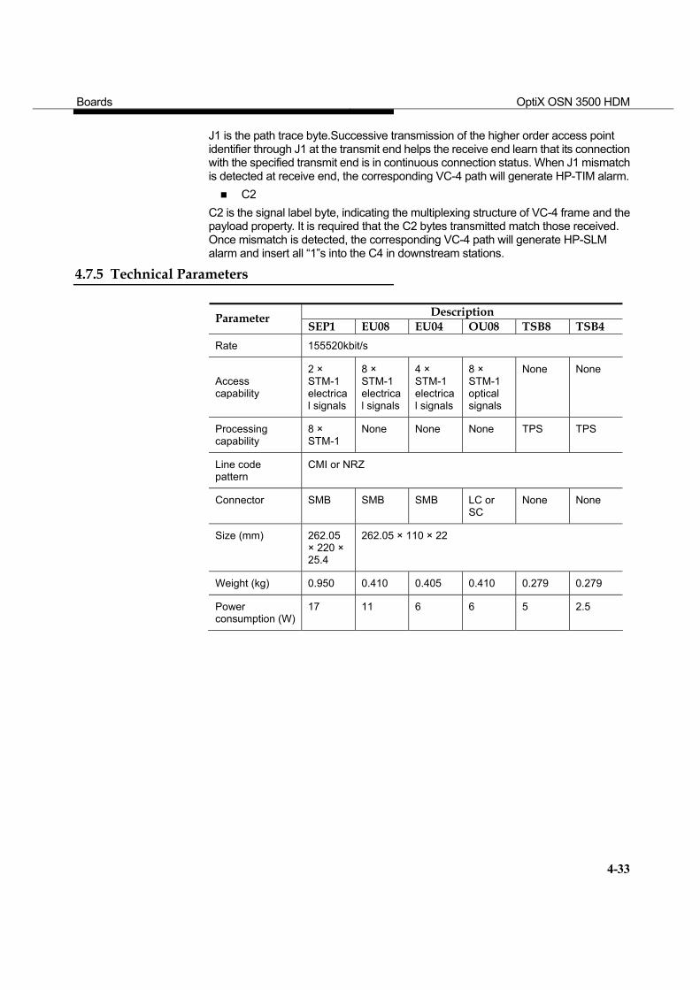
4.7.5 Technical Parameters
Description Parameter SEP1 EU08 EU04 OU08 TSB8 TSB4
Rate 155520kbit/s
Access capability
2 × STM-1 electrical signals
8 × STM-1 electrical signals
4 × STM-1 electrical signals
8 × STM-1 optical signals
None None
Processing capability
8 × STM-1
None None None TPS TPS
Line code pattern
CMI or NRZ
Connector SMB SMB SMB LC or SC
None None
Size (mm) 262.05 × 220 × 25.4
262.05 × 110 × 22
Weight (kg) 0.950 0.410 0.405 0.410 0.279 0.279
Power consumption (W)
17 11 6 6 5 2.5
Boards OptiX OSN 3500 HDM
4-34
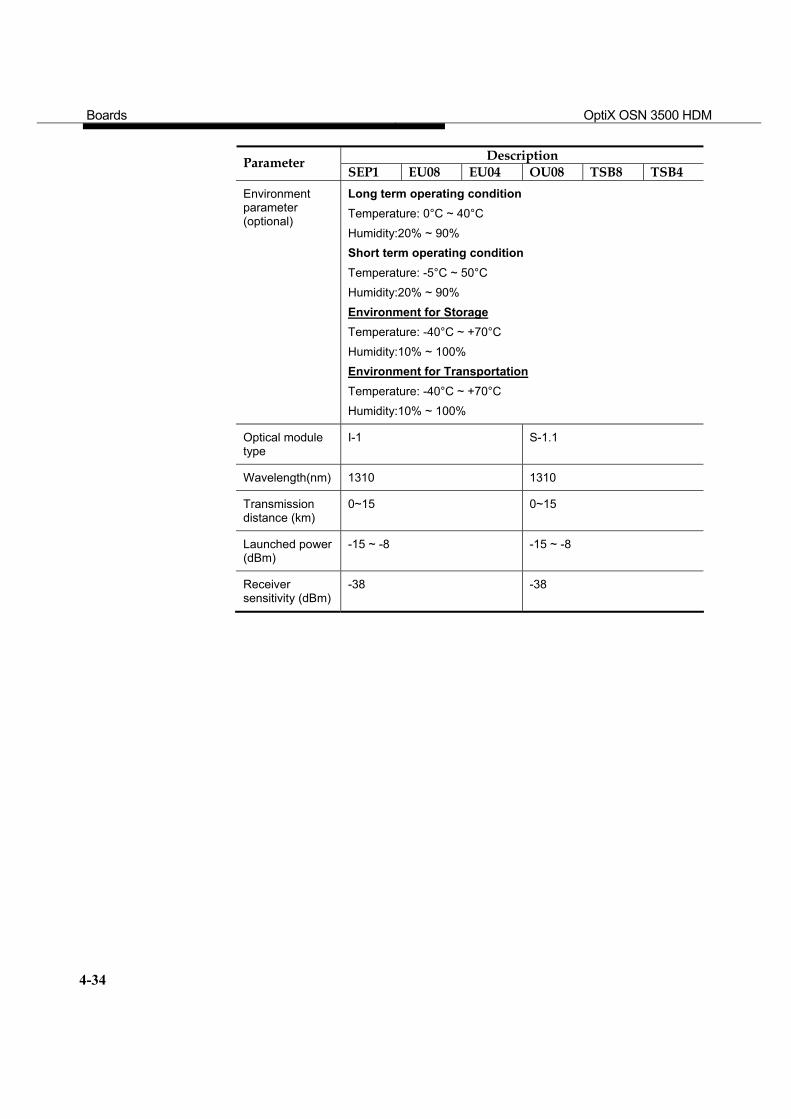
Description Parameter SEP1 EU08 EU04 OU08 TSB8 TSB4
Environment parameter (optional)
Long term operating condition Temperature: 0°C ~ 40°C Humidity:20% ~ 90% Short term operating condition Temperature: -5°C ~ 50°C Humidity:20% ~ 90% Environment for Storage Temperature: -40°C ~ +70°C Humidity:10% ~ 100% Environment for Transportation Temperature: -40°C ~ +70°C Humidity:10% ~ 100%
Optical module type
I-1 S-1.1
Wavelength(nm) 1310 1310
Transmission distance (km)
0~15 0~15
Launched power (dBm)
-15 ~ -8 -15 ~ -8
Receiver sensitivity (dBm)
-38 -38
Boards OptiX OSN 3500 HDM
4-35
4.8 SPQ4/MU04
SPQ4 is the 4 × E4/STM-1 processing board; and MU04 is the 4 x E4/STM-1 interface board. SPQ4 can work with MU04 to access and process 4 × E4/STM-1 electrical signals; and SPQ4 and MU04 can work with TSB4 to provide 1:N (N ≤ 3) TPS to SPQ4. SPQ4 can be seated in Slot 2 ~ 5 and 13 ~ 16 of the subrack, MU04 in Slot 19/21/23/25/29/31/33/35, and TSB4 in Slot 19/35.
4.8.1 Functions and Principles
1. Functions
Access and process 4 × E4/STM-1 electrical signals. All paths can be set for either E4 or STM-1 service as desired.
MU04 provides 75Ω SMB unbalanced interface. The STM-1 service supports such protection schemes as MSP and SNCP,
while the E4 service supports path protection (PP). Support SOH byte processing, including B1, B2, K1, K2, M1, F1 and D1 ~ 12. Support POH byte processing, including J1, B3, C2, G1 and H4. Provide abundant alarm and performance events for convenient equipment
management and maintenance. Support inloop and outloop at electrical interfaces for fast fault location. Support on-line query of the board information. Support configuration of such bytes as D1, D2 ~ D12, E1 and E2 to transparent
transmission or into other unused overhead bytes. Support smooth software upgrade and expansion.
2. Principles
Figure 4-11 shows the principle block diagram of SPQ4.
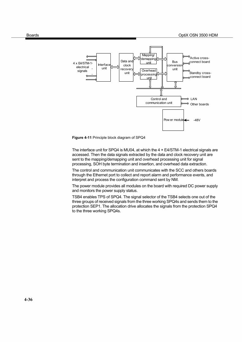
Boards OptiX OSN 3500 HDM
4-36
LAN
-48V
.
.
.
4 x E4/STM-1electricalsignals
Active cross-connect board
Interfaceunit
Data andclock
recoveryunit
Mapping/demapping
unit
Overheadprocessing
unit
Busconversion
unit
Control andcommunication unit
Pow er module
Standby cross-connect board
Other boards
Figure 4-11 Principle block diagram of SPQ4 The interface unit for SPQ4 is MU04, at which the 4 × E4/STM-1 electrical signals are accessed. Then the data signals extracted by the data and clock recovery unit are sent to the mapping/demapping unit and overhead processing unit for signal processing, SOH byte termination and insertion, and overhead data extraction. The control and communication unit communicates with the SCC and others boards through the Ethernet port to collect and report alarm and performance events, and interpret and process the configuration command sent by NM. The power module provides all modules on the board with required DC power supply and monitors the power supply status. TSB4 enables TPS of SPQ4. The signal selector of the TSB4 selects one out of the three groups of received signals from the three working SPQ4s and sends them to the protection SEP1. The allocation drive allocates the signals from the protection SPQ4 to the three working SPQ4s.
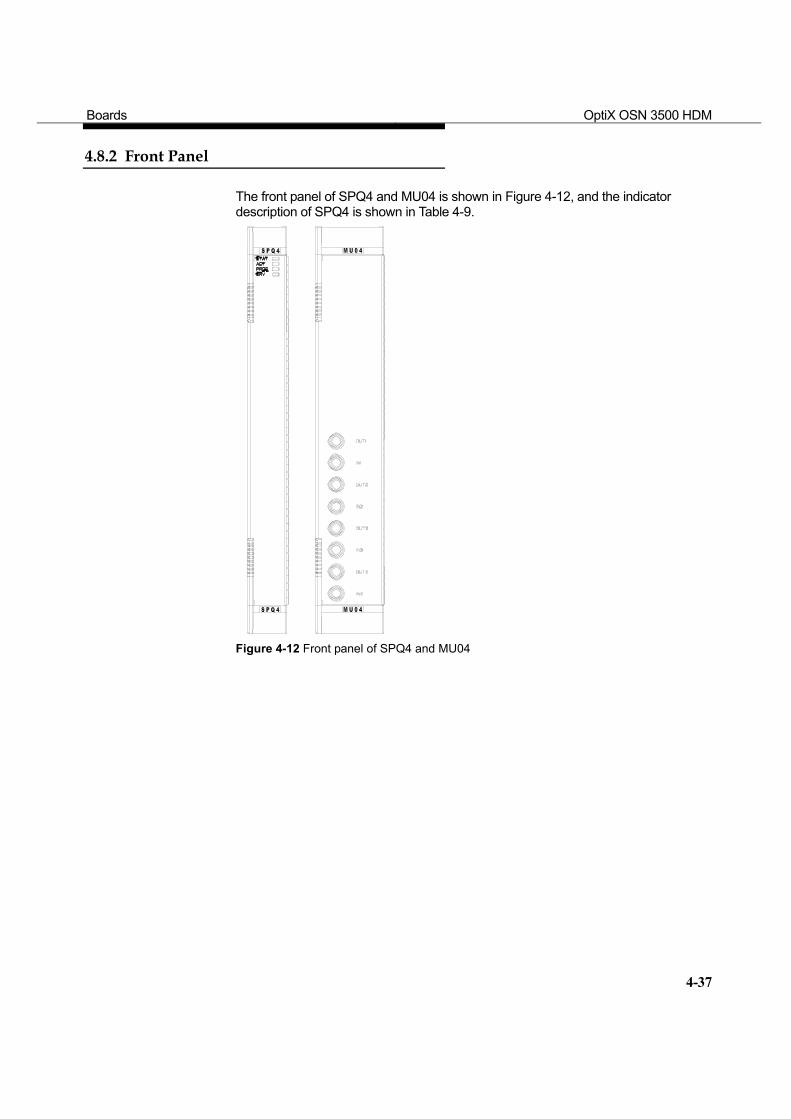
Boards OptiX OSN 3500 HDM
4-37
4.8.2 Front Panel
The front panel of SPQ4 and MU04 is shown in Figure 4-12, and the indicator description of SPQ4 is shown in Table 4-9.
Figure 4-12 Front panel of SPQ4 and MU04
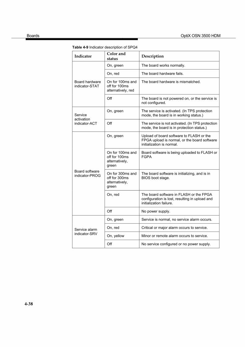
Boards OptiX OSN 3500 HDM
4-38
Table 4-9 Indicator description of SPQ4
Indicator Color and status Description
On, green The board works normally.
On, red The board hardware fails.
On for 100ms and off for 100ms alternatively, red
The board hardware is mismatched. Board hardware indicator-STAT
Off The board is not powered on, or the service is not configured.
On, green The service is activated. (In TPS protection mode, the board is in working status.) Service
activation indicator-ACT Off The service is not activated. (In TPS protection
mode, the board is in protection status.)
On, green Upload of board software to FLASH or the FPGA upload is normal, or the board software initialization is normal.
On for 100ms and off for 100ms alternatively, green
Board software is being uploaded to FLASH or FGPA
On for 300ms and off for 300ms alternatively, green
The board software is initializing, and is in BIOS boot stage.
On, red The board software in FLASH or the FPGA configuration is lost, resulting in upload and initialization failure.
Board software indicator-PROG
Off No power supply.
On, green Service is normal, no service alarm occurs.
On, red Critical or major alarm occurs to service.
On, yellow Minor or remote alarm occurs to service. Service alarm indicator-SRV
Off No service configured or no power supply.
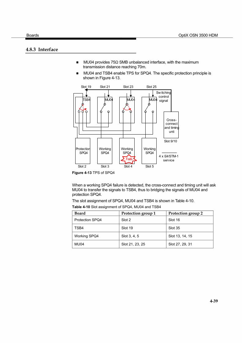
Boards OptiX OSN 3500 HDM
4-39
4.8.3 Interface
MU04 provides 75Ω SMB unbalanced interface, with the maximum transmission distance reaching 70m.
MU04 and TSB4 enable TPS for SPQ4. The specific protection principle is shown in Figure 4-13.
TSB4 MU04 MU04 MU04
Slot 21
ProtectionSPQ4
Slot 23 Slot 25Slot 19
Fails
WorkingSPQ4
WorkingSPQ4
WorkingSPQ4
Cross-connect
and timingunti
Sw itchingcontrolsignal
4 x E4/STM-1service
Slot 2
Slot 9/10
Slot 3 Slot 4 Slot 5 Figure 4-13 TPS of SPQ4 When a working SPQ4 failure is detected, the cross-connect and timing unit will ask MU04 to transfer the signals to TSB4, thus to bridging the signals of MU04 and protection SPQ4. The slot assignment of SPQ4, MU04 and TSB4 is shown in Table 4-10. Table 4-10 Slot assignment of SPQ4, MU04 and TSB4
Board Protection group 1 Protection group 2 Protection SPQ4 Slot 2 Slot 16
TSB4 Slot 19 Slot 35
Working SPQ4 Slot 3, 4, 5 Slot 13, 14, 15
MU04 Slot 21, 23, 25 Slot 27, 29, 31
Boards OptiX OSN 3500 HDM
4-40
Note: TPS is a scheme at device level. When the working board fails, the accessed signal will be protected by being bridged to the protection board. In this way, triggering of more complex protection at network level such as MSP and SNCP can be avoided, improving the equipment reliability.
4.8.4 Board Configuration
Before using SPQ4 for running service, parameters should be set for it through NM. Configuration should be provided to the following bytes:
J1 J1 is the path trace byte.Successive transmission of the higher order access point identifier through J1 at the transmit end helps the receive end learn that its connection with the specified transmit end is in continuous connection status. When J1 mismatch is detected at receive end, the corresponding VC-4 path will generate HP-TIM alarm.
C2 C2 is the signal label byte, indicating the multiplexing structure of VC-4 frame and the payload property. It is required that the C2 bytes transmitted match those received. Once mismatch is detected, the corresponding VC-4 path will generate HP-SLM alarm and insert all “1”s into the C4 in downstream stations.
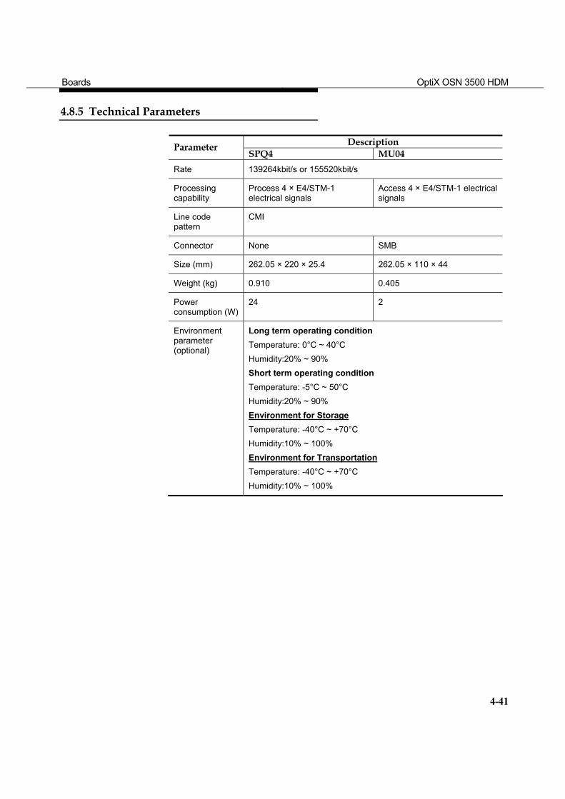
Boards OptiX OSN 3500 HDM
4-41
4.8.5 Technical Parameters
Description Parameter SPQ4 MU04
Rate 139264kbit/s or 155520kbit/s
Processing capability
Process 4 × E4/STM-1 electrical signals
Access 4 × E4/STM-1 electrical signals
Line code pattern
CMI
Connector None SMB
Size (mm) 262.05 × 220 × 25.4 262.05 × 110 × 44
Weight (kg) 0.910 0.405
Power consumption (W)
24 2
Environment parameter (optional)
Long term operating condition Temperature: 0°C ~ 40°C Humidity:20% ~ 90% Short term operating condition Temperature: -5°C ~ 50°C Humidity:20% ~ 90% Environment for Storage Temperature: -40°C ~ +70°C Humidity:10% ~ 100% Environment for Transportation Temperature: -40°C ~ +70°C Humidity:10% ~ 100%
Boards OptiX OSN 3500 HDM
4-42
4.9 PD3/PL3/D34S/C34S
PD3 is the 6 × E3/DS3 processing board; and PL3 is the 3 × E3/DS3 processing board. D34S is the 6 × E3/DS3 PDH interface switching board, C34S is the 3 × E3/DS3 PDH interface switching board. Table 4-11 shows the difference between PD3 and PL3. Table 4-11 Comparison between PD3 and PL3
Comparison Board name PD3 PL3
Processing capability 6 × E3/DS3 3 × E3/DS3
Available slots Slot 6~7, 12~13 Slot 6~7, 12~13
Interface board D34S C34S
4.9.1 Functions and Principles
1. Functions
PD3 can process 6 × E3/DS3 signals, and PL3 can process 3 × E3/DS3 signals.
D34S provides 6 × 75Ω unbalanced E3/DS3 interfaces, C34S provides 3 × 75Ω unbalanced E3/DS3 interfaces.
PD3/PL3 supports 1:N (N ≤ 3) TPS and SNCP, with the switching time less than 50ms.
Support setting and query of all POH bytes at VC-3 level. Provide abundant alarm and performance events for convenient equipment
management and maintenance. Support inloop and outloop at electrical interfaces for fast fault location. Support on-line query of the board information. Support smooth software upgrade and expansion.
2. Principles
Figure 4-14 shows the principle block diagram of PD3/PL3.
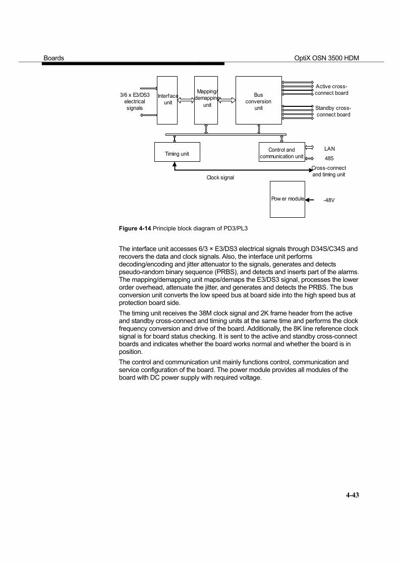
Boards OptiX OSN 3500 HDM
4-43
LAN
485
-48V
Standby cross-connect board
Interfaceunit
Active cross-connect board
Timing unitControl and
communication unit
Clock signal
Pow er module
Cross-connectand timing unit
Busconversion
unit
Mapping/demapping
unit
3/6 x E3/DS3electricalsignals
Figure 4-14 Principle block diagram of PD3/PL3 The interface unit accesses 6/3 × E3/DS3 electrical signals through D34S/C34S and recovers the data and clock signals. Also, the interface unit performs decoding/encoding and jitter attenuator to the signals, generates and detects pseudo-random binary sequence (PRBS), and detects and inserts part of the alarms. The mapping/demapping unit maps/demaps the E3/DS3 signal, processes the lower order overhead, attenuate the jitter, and generates and detects the PRBS. The bus conversion unit converts the low speed bus at board side into the high speed bus at protection board side. The timing unit receives the 38M clock signal and 2K frame header from the active and standby cross-connect and timing units at the same time and performs the clock frequency conversion and drive of the board. Additionally, the 8K line reference clock signal is for board status checking. It is sent to the active and standby cross-connect boards and indicates whether the board works normal and whether the board is in position. The control and communication unit mainly functions control, communication and service configuration of the board. The power module provides all modules of the board with DC power supply with required voltage.
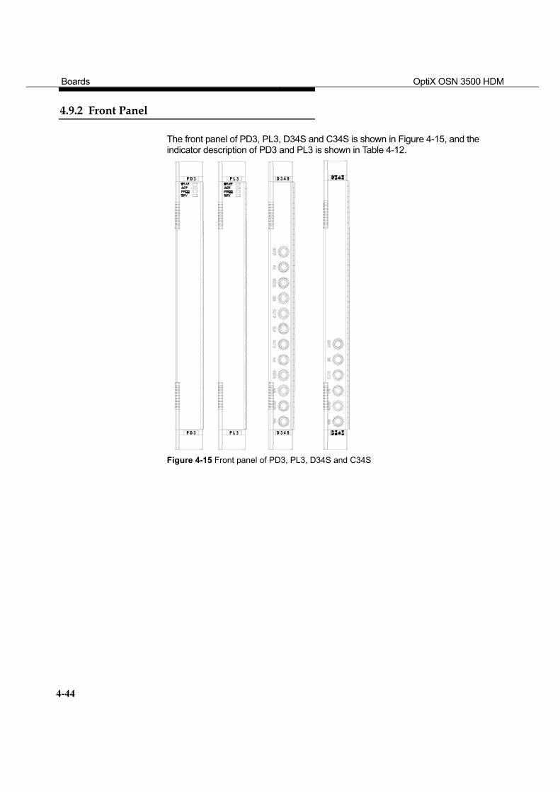
Boards OptiX OSN 3500 HDM
4-44
4.9.2 Front Panel
The front panel of PD3, PL3, D34S and C34S is shown in Figure 4-15, and the indicator description of PD3 and PL3 is shown in Table 4-12.
Figure 4-15 Front panel of PD3, PL3, D34S and C34S

Boards OptiX OSN 3500 HDM
4-45
Table 4-12 Indicator description of PD3/PL3
Indicator Color and status Description
On, green The board works normally.
On, red The board hardware fails.
On for 100ms and off for 100ms alternatively, red
The board hardware is mismatched. Board hardware indicator-STAT
Off The board is not powered on, or the service is not configured.
On, green The service is activated. (In TPS protection mode, the board is in working status.) Service
activation indicator-ACT Off The service is not activated. (In TPS protection
mode, the board is in protection status.)
On, green Upload of board software to FLASH or the FPGA upload is normal, or the board software initialization is normal.
On for 100ms and off for 100ms alternatively, green
Board software is being uploaded to FLASH or FGPA
On for 300ms and off for 300ms alternatively, green
The board software is initializing, and is in BIOS boot stage.
On, red The board software in FLASH or the FPGA configuration is lost, resulting in upload and initialization failure.
Board software indicator-PROG
Off No power supply.
On, green Service is normal, no service alarm occurs.
On, red Critical or major alarm occurs to service.
On, yellow Minor or remote alarm occurs to service. Service alarm indicator-SRV
Off No service configured or no power supply.
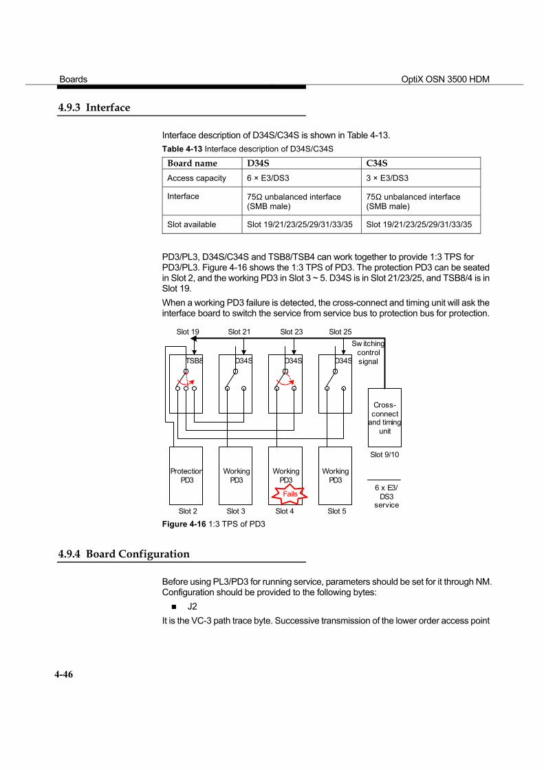
Boards OptiX OSN 3500 HDM
4-46
4.9.3 Interface
Interface description of D34S/C34S is shown in Table 4-13. Table 4-13 Interface description of D34S/C34S
Board name D34S C34S Access capacity 6 × E3/DS3 3 × E3/DS3
Interface 75Ω unbalanced interface (SMB male)
75Ω unbalanced interface (SMB male)
Slot available Slot 19/21/23/25/29/31/33/35 Slot 19/21/23/25/29/31/33/35
PD3/PL3, D34S/C34S and TSB8/TSB4 can work together to provide 1:3 TPS for PD3/PL3. Figure 4-16 shows the 1:3 TPS of PD3. The protection PD3 can be seated in Slot 2, and the working PD3 in Slot 3 ~ 5. D34S is in Slot 21/23/25, and TSB8/4 is in Slot 19. When a working PD3 failure is detected, the cross-connect and timing unit will ask the interface board to switch the service from service bus to protection bus for protection.
TSB8 D34S D34S D34S
Slot 23Slot 19 Slot 21
Slot 2
Slot 25
Slot 9/10
Slot 3 Slot 4 Slot 5
ProtectionPD3
WorkingPD3
WorkingPD3
WorkingPD3
Cross-connect
and timingunit
Sw itchingcontrolsignal
6 x E3/DS3
serviceFails
Figure 4-16 1:3 TPS of PD3
4.9.4 Board Configuration
Before using PL3/PD3 for running service, parameters should be set for it through NM. Configuration should be provided to the following bytes:
J2 It is the VC-3 path trace byte. Successive transmission of the lower order access point
Boards OptiX OSN 3500 HDM
4-47
identifier through J1 helps the receive end learn that its connection with the transmit end in this path is in continuous connection status.
4.9.5 Technical Specifications
Description Parameter PL3 PD3 D34S C34S
Rate 34368kbit/s or 44736kbit/s
Processing capability
Process 3 × E3/DS3
Process 6 × E3/DS3
Access 6 × E3/DS3
Access 3 × E3/DS3
Line code pattern
E3:HDB3, DS3:B3ZS
Connector None None SMB SMB
Size (mm) 262.05 × 220 × 25.4 262.05 × 110 × 22
Weight (kg) 0.995 1.120 0.381 0.310
Power consumption (W)
15 19 2 2
Environment parameter (optional)
Long term operating condition Temperature: 0°C ~ 40°C Humidity:20% ~ 90% Short term operating condition Temperature: -5°C ~ 50°C Humidity:20% ~ 90% Environment for Storage Temperature: -40°C ~ +70°C Humidity:10% ~ 100% Environment for Transportation Temperature: -40°C ~ +70°C Humidity:10% ~ 100%
Boards OptiX OSN 3500 HDM
4-48
4.10 PQ1/PQM/D75S/D12S/D12B
PQ1 is the 63 × E1 processing board; PQM is the 63 × E1/T1 processing board; D75S is the 32 × 75Ω E1 PDH interface switching board; D12S is the 32 × 120Ω E1/T1 PDH interface switching board; D12B is the 32 × 75Ω/120Ω E1/T1 PDH interface board. D75S, D12S and D12B can work as interfaces boards to receive/transmit E1/T1 service for PQ1/PQM. D75S and D12S can also work as switching boards to implement TPS for PQ1/PQM. Table 4-14 shows the difference between PQ1 and PQM. Table 4-14 Comparison between PQ1 and PQM
Board name Comparison PQ1 PQM
Processing capability 63 × E1 63 × E1/T1
Interface board (Providing TPS)
2 × D75S or 2 × D12S 2 × D12S
Interface board (NOT providing TPS)
2 × D12B 2 × D12B
4.10.1 Functions and Principles
1. Functions
D75S provides 32 × 75Ω unbalanced E1 interfaces; D12S provides 32 × 120Ω balanced E1/T1 interfaces; and D12B provides 32 × 75Ω/120Ω E1/T1 interfaces.
PQM processes 63 × E1/T1 signals, each of which can be configured as either E1 or T1 independently through software. PQ1 processes 63 × E1 signals.
PQ1/PQM supports 1:N (N ≤ 8) TPS, PP and SNCP, with the switching time less than 50ms.
Provide abundant alarm and performance events for convenient equipment management and maintenance.
Support inloop and outloop at electrical interfaces for fast fault location. Support on-line query of the board information. Support smooth software upgrade and expansion.
2. Principles
Figure 4-17 shows the principle block diagram of PQ1/PQM.
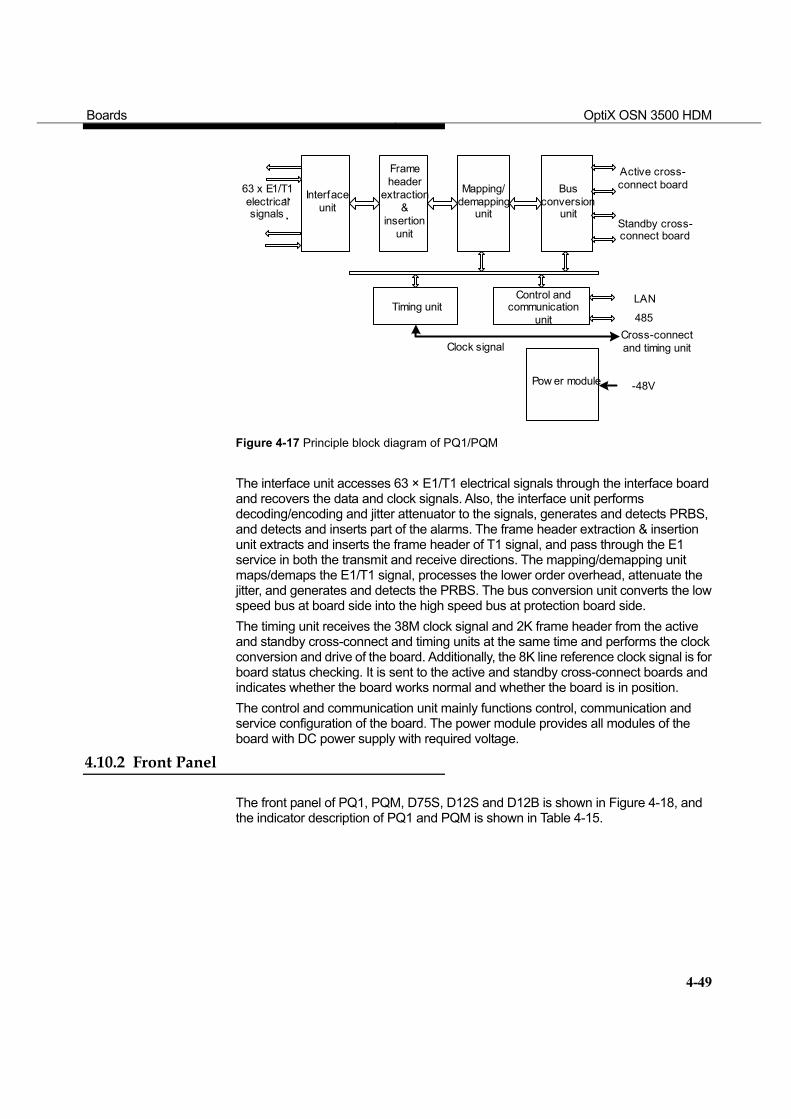
Boards OptiX OSN 3500 HDM
4-49
LAN
485
-48V
...
Mapping/demapping
unit
63 x E1/T1electricalsignals
Interfaceunit
Frameheader
extraction&
insertionunit
Standby cross-connect board
Busconversion
unit
Active cross-connect board
Timing unitControl and
communicationunit
Cross-connectand timing unitClock signal
Pow er module
Figure 4-17 Principle block diagram of PQ1/PQM The interface unit accesses 63 × E1/T1 electrical signals through the interface board and recovers the data and clock signals. Also, the interface unit performs decoding/encoding and jitter attenuator to the signals, generates and detects PRBS, and detects and inserts part of the alarms. The frame header extraction & insertion unit extracts and inserts the frame header of T1 signal, and pass through the E1 service in both the transmit and receive directions. The mapping/demapping unit maps/demaps the E1/T1 signal, processes the lower order overhead, attenuate the jitter, and generates and detects the PRBS. The bus conversion unit converts the low speed bus at board side into the high speed bus at protection board side. The timing unit receives the 38M clock signal and 2K frame header from the active and standby cross-connect and timing units at the same time and performs the clock conversion and drive of the board. Additionally, the 8K line reference clock signal is for board status checking. It is sent to the active and standby cross-connect boards and indicates whether the board works normal and whether the board is in position. The control and communication unit mainly functions control, communication and service configuration of the board. The power module provides all modules of the board with DC power supply with required voltage.
4.10.2 Front Panel
The front panel of PQ1, PQM, D75S, D12S and D12B is shown in Figure 4-18, and the indicator description of PQ1 and PQM is shown in Table 4-15.
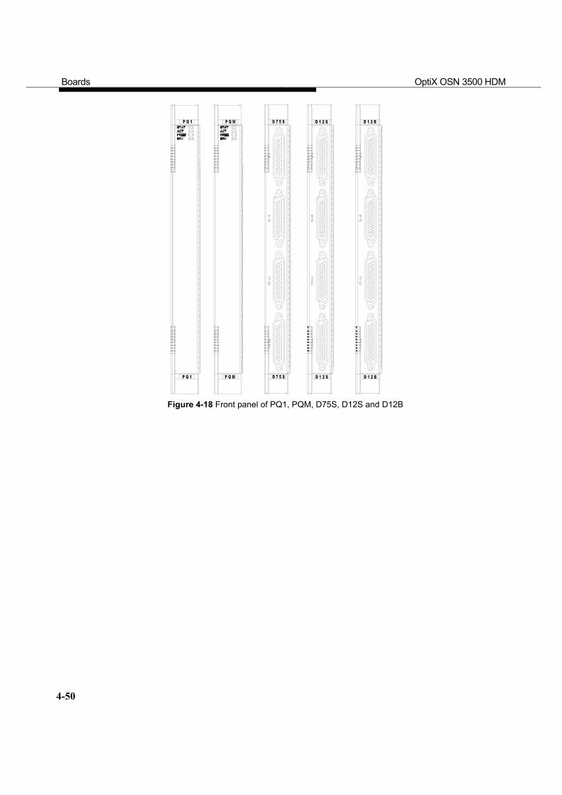
Boards OptiX OSN 3500 HDM
4-50
Figure 4-18 Front panel of PQ1, PQM, D75S, D12S and D12B
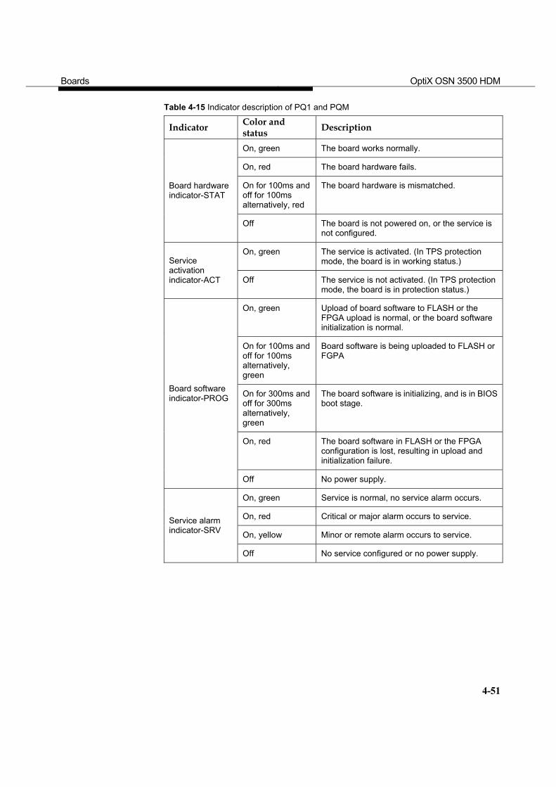
Boards OptiX OSN 3500 HDM
4-51
Table 4-15 Indicator description of PQ1 and PQM
Indicator Color and status Description
On, green The board works normally.
On, red The board hardware fails.
On for 100ms and off for 100ms alternatively, red
The board hardware is mismatched. Board hardware indicator-STAT
Off The board is not powered on, or the service is not configured.
On, green The service is activated. (In TPS protection mode, the board is in working status.) Service
activation indicator-ACT Off The service is not activated. (In TPS protection
mode, the board is in protection status.)
On, green Upload of board software to FLASH or the FPGA upload is normal, or the board software initialization is normal.
On for 100ms and off for 100ms alternatively, green
Board software is being uploaded to FLASH or FGPA
On for 300ms and off for 300ms alternatively, green
The board software is initializing, and is in BIOS boot stage.
On, red The board software in FLASH or the FPGA configuration is lost, resulting in upload and initialization failure.
Board software indicator-PROG
Off No power supply.
On, green Service is normal, no service alarm occurs.
On, red Critical or major alarm occurs to service.
On, yellow Minor or remote alarm occurs to service. Service alarm indicator-SRV
Off No service configured or no power supply.
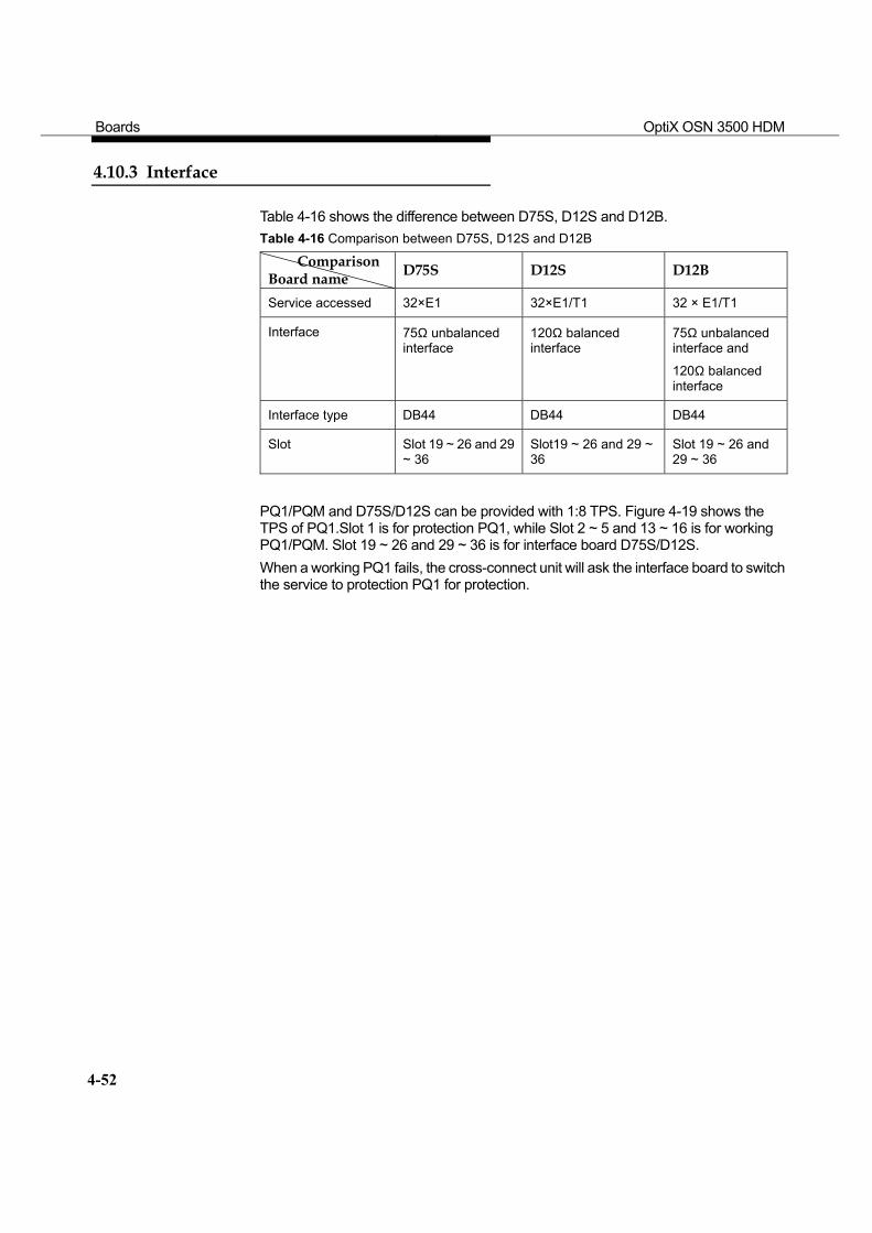
Boards OptiX OSN 3500 HDM
4-52
4.10.3 Interface
Table 4-16 shows the difference between D75S, D12S and D12B. Table 4-16 Comparison between D75S, D12S and D12B
Comparison Board name D75S D12S D12B
Service accessed 32×E1 32×E1/T1 32 × E1/T1
Interface 75Ω unbalanced interface
120Ω balanced interface
75Ω unbalanced interface and
120Ω balanced interface
Interface type DB44 DB44 DB44
Slot Slot 19 ~ 26 and 29 ~ 36
Slot19 ~ 26 and 29 ~ 36
Slot 19 ~ 26 and 29 ~ 36
PQ1/PQM and D75S/D12S can be provided with 1:8 TPS. Figure 4-19 shows the TPS of PQ1.Slot 1 is for protection PQ1, while Slot 2 ~ 5 and 13 ~ 16 is for working PQ1/PQM. Slot 19 ~ 26 and 29 ~ 36 is for interface board D75S/D12S. When a working PQ1 fails, the cross-connect unit will ask the interface board to switch the service to protection PQ1 for protection.
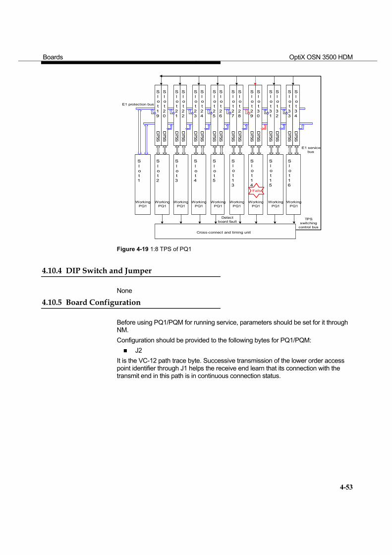
Boards OptiX OSN 3500 HDM
4-53
Slot1
Slot2
Slot3
Slot4
Slot5
Slot13
Slot14
Slot15
Slot16
Slot19
Slot20
Slot21
Slot22
Slot23
Slot24
Slot25
Slot26
Slot28
Slot29
Slot30
Slot31
Slot32
Slot33
Slot34
Slot27
D75S
D75S
D75S
D75S
D75S
D75S
D75S
D75S
D75S
D75S
D75S
D75S
D75S
D75S
D75S
D75S
Fails
E1 protection bus
E1 servicebus
TPSswitching
control busCross-connect and timing unit
Detectboard fault
WorkingPQ1
WorkingPQ1
WorkingPQ1
WorkingPQ1
WorkingPQ1
WorkingPQ1
WorkingPQ1
WorkingPQ1
WorkingPQ1
Figure 4-19 1:8 TPS of PQ1
4.10.4 DIP Switch and Jumper
None
4.10.5 Board Configuration
Before using PQ1/PQM for running service, parameters should be set for it through NM. Configuration should be provided to the following bytes for PQ1/PQM:
J2 It is the VC-12 path trace byte. Successive transmission of the lower order access point identifier through J1 helps the receive end learn that its connection with the transmit end in this path is in continuous connection status.
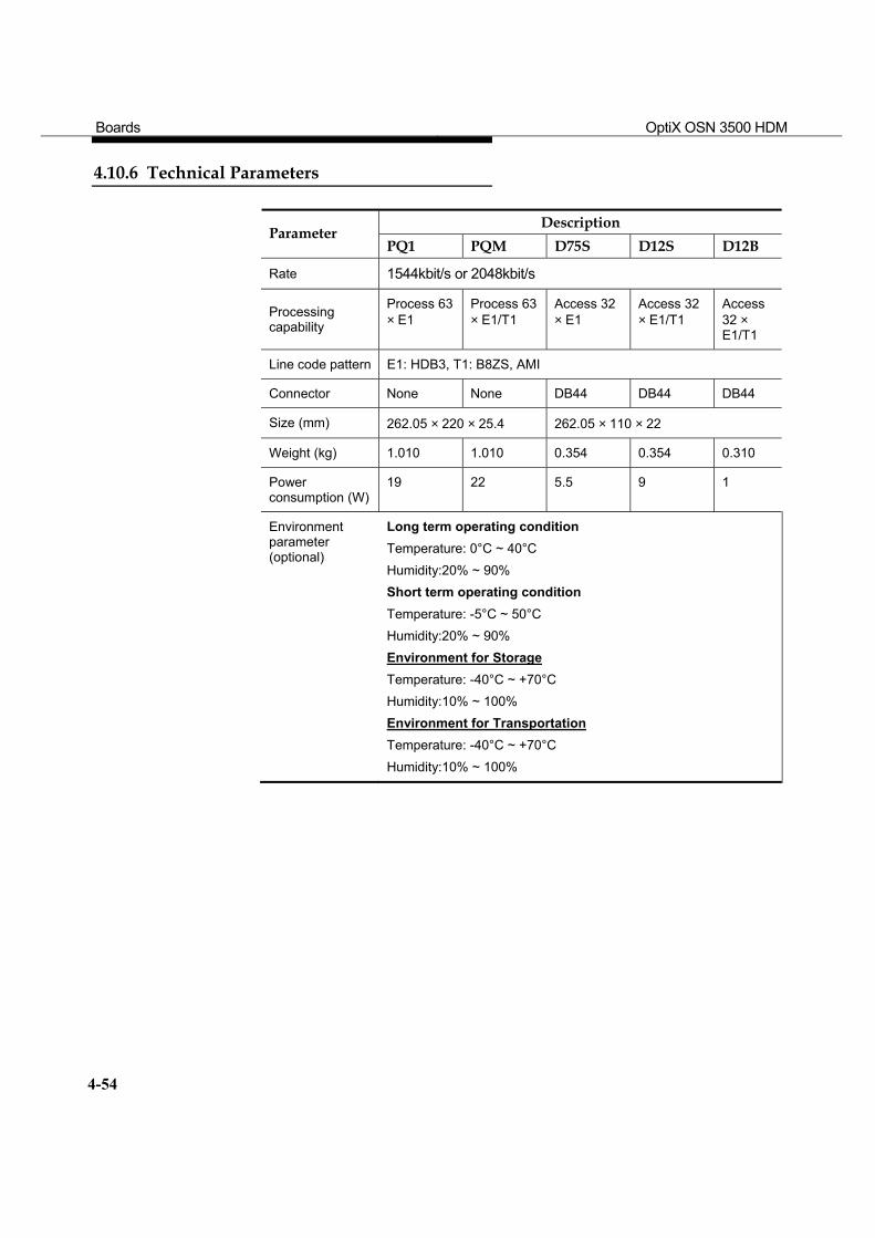
Boards OptiX OSN 3500 HDM
4-54
4.10.6 Technical Parameters
Description Parameter
PQ1 PQM D75S D12S D12B
Rate 1544kbit/s or 2048kbit/s
Processing capability
Process 63 × E1
Process 63 × E1/T1
Access 32 × E1
Access 32 × E1/T1
Access 32 × E1/T1
Line code pattern E1: HDB3, T1: B8ZS, AMI
Connector None None DB44 DB44 DB44
Size (mm) 262.05 × 220 × 25.4 262.05 × 110 × 22
Weight (kg) 1.010 1.010 0.354 0.354 0.310
Power consumption (W)
19 22 5.5 9 1
Environment parameter (optional)
Long term operating condition Temperature: 0°C ~ 40°C Humidity:20% ~ 90% Short term operating condition Temperature: -5°C ~ 50°C Humidity:20% ~ 90% Environment for Storage Temperature: -40°C ~ +70°C Humidity:10% ~ 100% Environment for Transportation Temperature: -40°C ~ +70°C Humidity:10% ~ 100%
Boards OptiX OSN 3500 HDM
4-55
4.11 EGS2
EGS2 is the 2-port Gigabit Ethernet optical interface board with Lanswitch. EGS2 can transparently transmit and converge the GE service. When working together with EFS0 and EFS4, the FE service can be converged into GE service and the Layer 2 switching can be performed. EGS2 can be seated in Slot 6 ~ 8 or 11 ~ 13 when the subrack cross-connect capacity is 40G, and in Slot 5 ~ 8 or 11 ~ 14 when the subrack cross-connect capacity is 80G.
4.11.1 Functions and Principles
1. Functions
Provides 2 × LC 1000BASE-SX/LX Ethernet optical interfaces with auto-negotiation function, that is, they can be set to enabled or disabled. The transmission distance of the interfaces is 500m (multimode) or 10km (single-mode), or you can select the 40km or 70km optical module as required in practice.
Support bandwidth adjustment at granularity of 64kbit/s and service mapping into VC-12 or VC-3 level. The service supports global functional plane (GFP), link access procedure-SDH (LAPS) and high-level data link control (HDLC) encapsulation.
support Link capacity adjustment scheme (LCAS), achieving higher transmission bandwidth utility.
Support the Ethernet Layer 2 switching, rapid spanning tree protocol (RSTP), and point-to-point and point-to-multipoint multiprotocol label switching (MPLS) Layer 2 virtual private network (VPN).
Support IEEE 802.1q-compliant and IEEE 802.1p-compliant virtual local area network (VLAN) and VLAN convergence.
Support Layer 2-based convergence and point-to-multipoint convergence. EGS2 can work with EFS0 and EFS4 to converge the FE service into GE
service. Support the port-based and port + VLAN-based flow classification, and the
priority setting and queue adjusting of flow. Support IEEE802.3x-compliant flow control. Support inloop and outloop of all kinds for fast fault location. Provide abundant alarm and performance events for convenient equipment
management and maintenance.
2. Principles
Figure 4-20 shows the principle block diagram of EGS2.
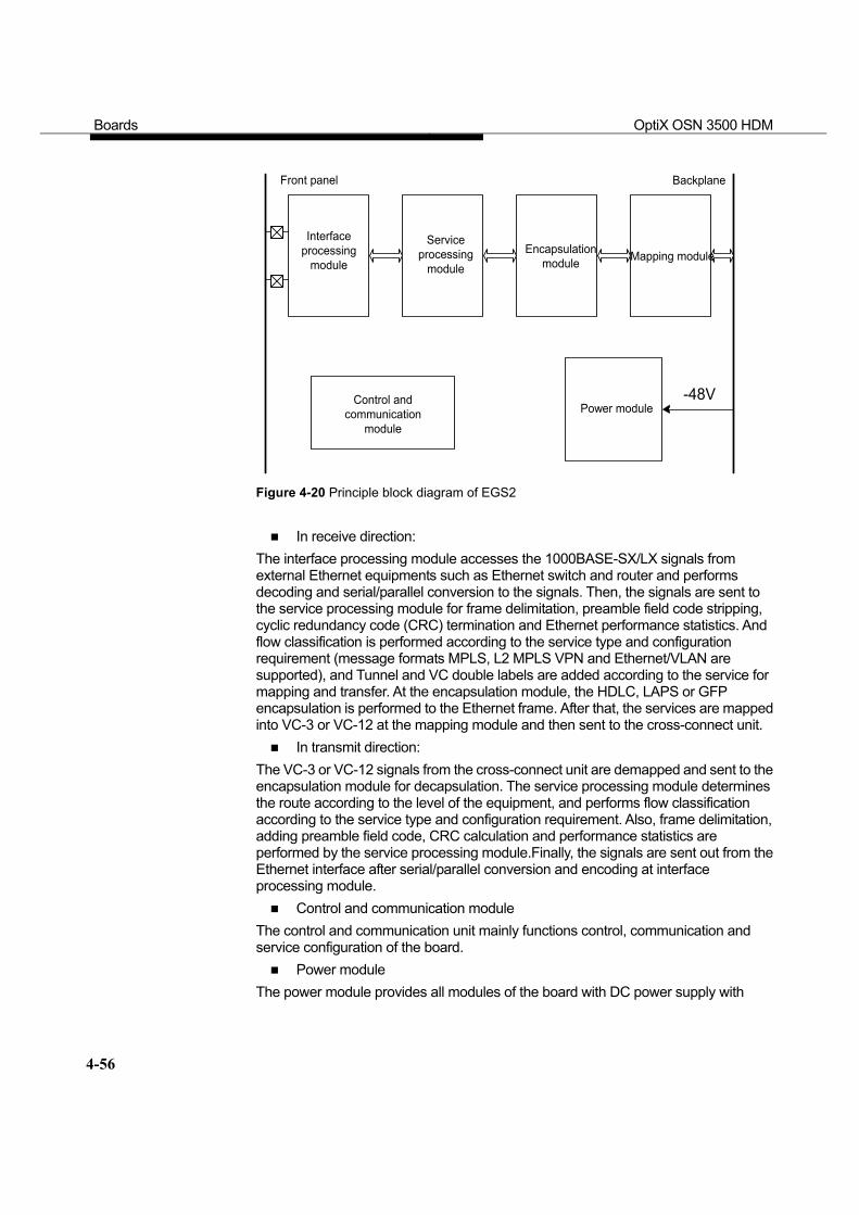
Boards OptiX OSN 3500 HDM
4-56
-48V
Serviceprocessing
module
Front panel Backplane
Interfaceprocessing
module
Power module
Encapsulationmodule Mapping module
Control andcommunication
module
Figure 4-20 Principle block diagram of EGS2
In receive direction: The interface processing module accesses the 1000BASE-SX/LX signals from external Ethernet equipments such as Ethernet switch and router and performs decoding and serial/parallel conversion to the signals. Then, the signals are sent to the service processing module for frame delimitation, preamble field code stripping, cyclic redundancy code (CRC) termination and Ethernet performance statistics. And flow classification is performed according to the service type and configuration requirement (message formats MPLS, L2 MPLS VPN and Ethernet/VLAN are supported), and Tunnel and VC double labels are added according to the service for mapping and transfer. At the encapsulation module, the HDLC, LAPS or GFP encapsulation is performed to the Ethernet frame. After that, the services are mapped into VC-3 or VC-12 at the mapping module and then sent to the cross-connect unit.
In transmit direction: The VC-3 or VC-12 signals from the cross-connect unit are demapped and sent to the encapsulation module for decapsulation. The service processing module determines the route according to the level of the equipment, and performs flow classification according to the service type and configuration requirement. Also, frame delimitation, adding preamble field code, CRC calculation and performance statistics are performed by the service processing module.Finally, the signals are sent out from the Ethernet interface after serial/parallel conversion and encoding at interface processing module.
Control and communication module The control and communication unit mainly functions control, communication and service configuration of the board.
Power module The power module provides all modules of the board with DC power supply with

Boards OptiX OSN 3500 HDM
4-57
required voltage.
4.11.2 Front Panel
Front panel and indicator description of EGS2 is shown in Table 4-17.
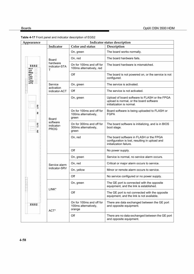
Boards OptiX OSN 3500 HDM
4-58
Table 4-17 Front panel and indicator description of EGS2
Appearance Indicator status description Indicator Color and status Description
On, green The board works normally.
On, red The board hardware fails.
On for 100ms and off for 100ms alternatively, red
The board hardware is mismatched.
Board hardware indicator-STAT
Off The board is not powered on, or the service is not configured.
On, green The service is activated. Service activation indicator-ACT Off The service is not activated.
On, green Upload of board software to FLASH or the FPGA upload is normal, or the board software initialization is normal.
On for 100ms and off for 100ms alternatively, green
Board software is being uploaded to FLASH or FGPA
On for 300ms and off for 300ms alternatively, green
The board software is initializing, and is in BIOS boot stage.
On, red The board software in FLASH or the FPGA configuration is lost, resulting in upload and initialization failure.
Board software indicator- PROG
Off No power supply.
On, green Service is normal, no service alarm occurs.
On, red Critical or major alarm occurs to service.
On, yellow Minor or remote alarm occurs to service. Service alarm indicator-SRV
Off No service configured or no power supply.
On, green The GE port is connected with the opposite equipment, and the link is established.
LINK* Off The GE port is not connected with the opposite
equipment, and the link is not available.
On for 100ms and off for 100ms alternatively, orange
There are data exchanged between the GE port and opposite equipment.
ACT*
Off There are no data exchanged between the GE port and opposite equipment.
Boards OptiX OSN 3500 HDM
4-59
4.11.3 Interface
EGS2 supports the small-form pluggable (SFP) LC optical interface, and 1000Base-SX and 1000Base-LX interfaces. The interface transmission distance reaches 550m (multimode) or 10km (single-mode). Table 4-18 shows the interface characteristics of EGS2. Table 4-18 Interface characteristics of EGS2
Connector LC
Optical interface type 1000Base-SX or 1000Base-LX
Specifications IEEE 802.3z-compliant
Line code Manchester coding (10M), MLT-3 or NRZI
4.11.4 DIP Switch and Jumper
None
4.11.5 Board Configuration
Before using EGS2 for running service, parameters should be set for it through NM. Configuration should be provided to the following items:
J1 J1 is the path trace byte.Successive transmission of the higher order access point identifier through J1 at the transmit end helps the receive end learn that its connection with the specified transmit end is in continuous connection status. When J1 mismatch is detected at receive end, the corresponding VC-4 path will generate HP-TIM alarm.
C2 C2 is the signal label byte, indicating the multiplexing structure of VC-4 frame and the payload property. It is required that the C2 bytes transmitted match those received. Once mismatch is detected, the corresponding VC-4 path will generate HP-SLM alarm and insert all “1”s into the C4 in downstream stations.
Ethernet port working mode The Ethernet ports of the interconnected equipments are generally required to work in the same fixed mode. If not, packet loss or rate decrease will happen, and even complete service interruption will be resulted when the traffic is heavy.
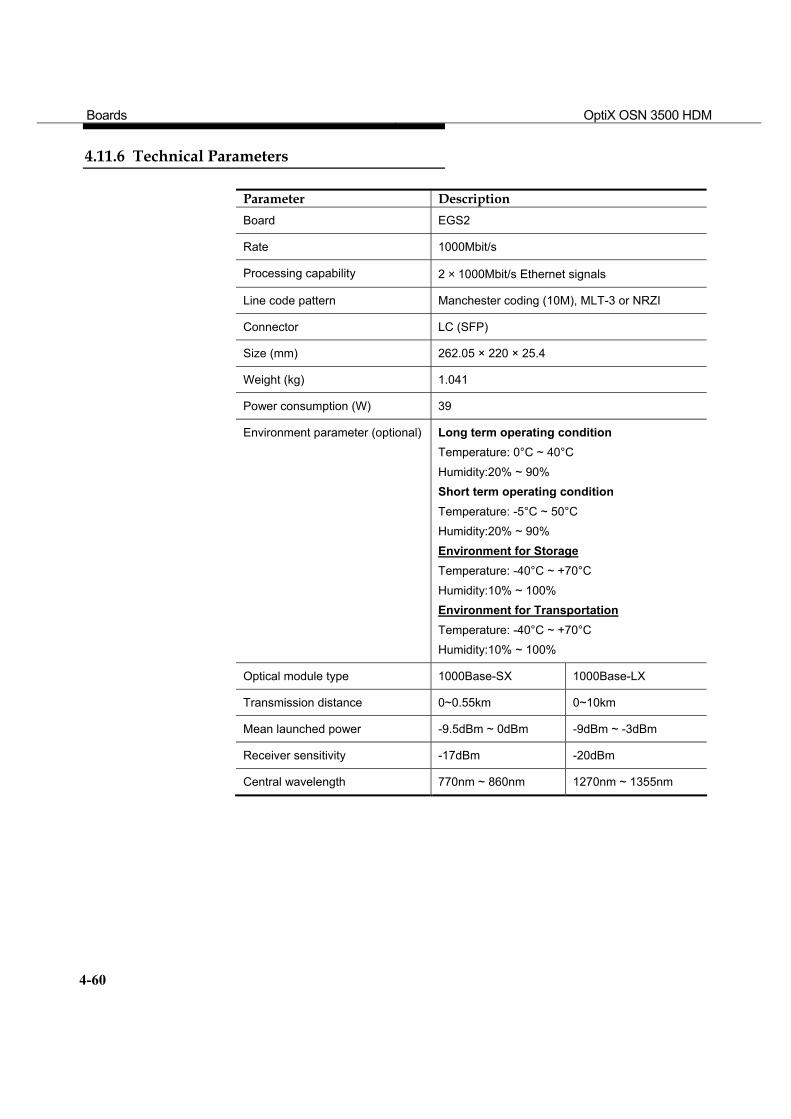
Boards OptiX OSN 3500 HDM
4-60
4.11.6 Technical Parameters
Parameter Description Board EGS2
Rate 1000Mbit/s
Processing capability 2 × 1000Mbit/s Ethernet signals
Line code pattern Manchester coding (10M), MLT-3 or NRZI
Connector LC (SFP)
Size (mm) 262.05 × 220 × 25.4
Weight (kg) 1.041
Power consumption (W) 39
Environment parameter (optional) Long term operating condition Temperature: 0°C ~ 40°C Humidity:20% ~ 90% Short term operating condition Temperature: -5°C ~ 50°C Humidity:20% ~ 90% Environment for Storage Temperature: -40°C ~ +70°C Humidity:10% ~ 100% Environment for Transportation Temperature: -40°C ~ +70°C Humidity:10% ~ 100%
Optical module type 1000Base-SX 1000Base-LX
Transmission distance 0~0.55km 0~10km
Mean launched power -9.5dBm ~ 0dBm -9dBm ~ -3dBm
Receiver sensitivity -17dBm -20dBm
Central wavelength 770nm ~ 860nm 1270nm ~ 1355nm
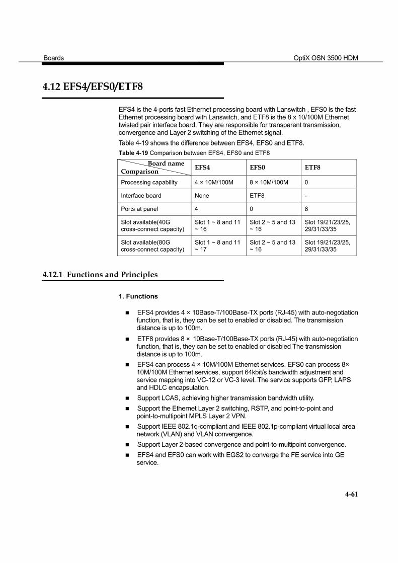
Boards OptiX OSN 3500 HDM
4-61
4.12 EFS4/EFS0/ETF8
EFS4 is the 4-ports fast Ethernet processing board with Lanswitch , EFS0 is the fast Ethernet processing board with Lanswitch, and ETF8 is the 8 x 10/100M Ethernet twisted pair interface board. They are responsible for transparent transmission, convergence and Layer 2 switching of the Ethernet signal. Table 4-19 shows the difference between EFS4, EFS0 and ETF8. Table 4-19 Comparison between EFS4, EFS0 and ETF8
Board name Comparison EFS4 EFS0 ETF8
Processing capability 4 × 10M/100M 8 × 10M/100M 0
Interface board None ETF8 -
Ports at panel 4 0 8
Slot available(40G cross-connect capacity)
Slot 1 ~ 8 and 11 ~ 16
Slot 2 ~ 5 and 13 ~ 16
Slot 19/21/23/25, 29/31/33/35
Slot available(80G cross-connect capacity)
Slot 1 ~ 8 and 11 ~ 17
Slot 2 ~ 5 and 13 ~ 16
Slot 19/21/23/25, 29/31/33/35
4.12.1 Functions and Principles
1. Functions
EFS4 provides 4 × 10Base-T/100Base-TX ports (RJ-45) with auto-negotiation function, that is, they can be set to enabled or disabled. The transmission distance is up to 100m.
ETF8 provides 8 × 10Base-T/100Base-TX ports (RJ-45) with auto-negotiation function, that is, they can be set to enabled or disabled The transmission distance is up to 100m.
EFS4 can process 4 × 10M/100M Ethernet services. EFS0 can process 8× 10M/100M Ethernet services, support 64kbit/s bandwidth adjustment and service mapping into VC-12 or VC-3 level. The service supports GFP, LAPS and HDLC encapsulation.
Support LCAS, achieving higher transmission bandwidth utility. Support the Ethernet Layer 2 switching, RSTP, and point-to-point and
point-to-multipoint MPLS Layer 2 VPN. Support IEEE 802.1q-compliant and IEEE 802.1p-compliant virtual local area
network (VLAN) and VLAN convergence. Support Layer 2-based convergence and point-to-multipoint convergence. EFS4 and EFS0 can work with EGS2 to converge the FE service into GE
service.
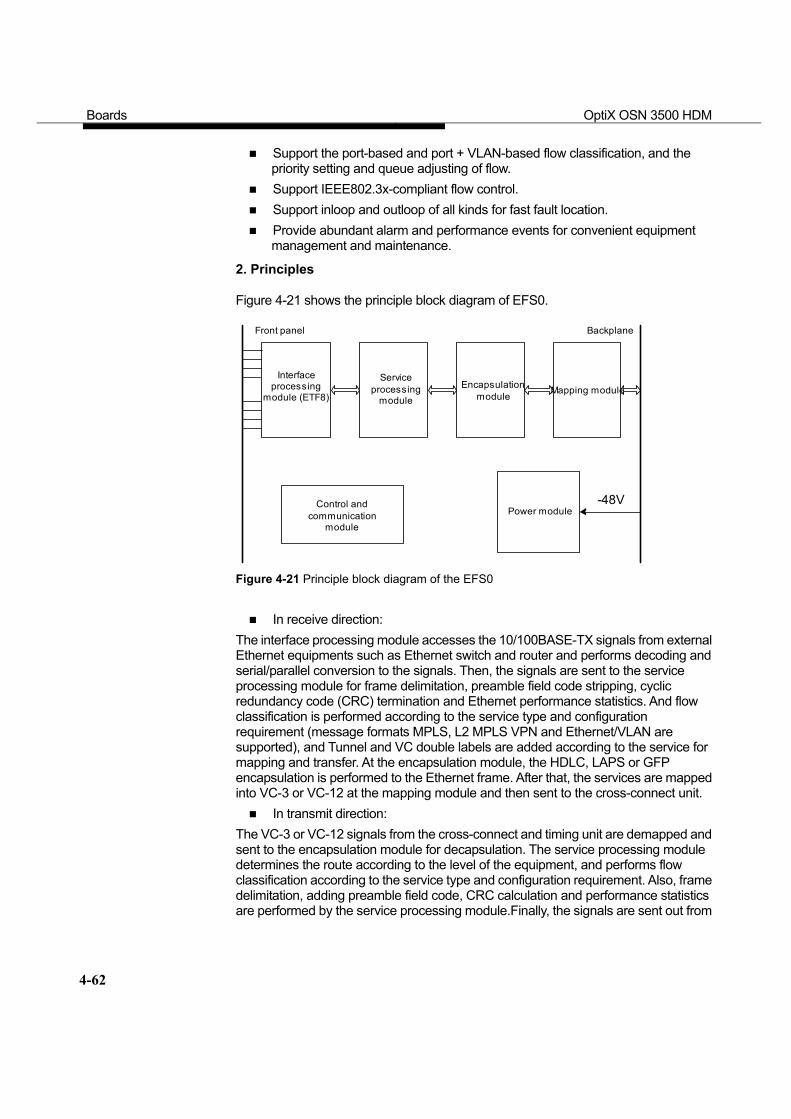
Boards OptiX OSN 3500 HDM
4-62
Support the port-based and port + VLAN-based flow classification, and the priority setting and queue adjusting of flow.
Support IEEE802.3x-compliant flow control. Support inloop and outloop of all kinds for fast fault location. Provide abundant alarm and performance events for convenient equipment
management and maintenance.
2. Principles
Figure 4-21 shows the principle block diagram of EFS0.
-48V
Serviceprocessing
module
Front panel Backplane
Interfaceprocessing
module (ETF8)
Power module
Encapsulationmodule Mapping module
Control andcommunication
module
Figure 4-21 Principle block diagram of the EFS0
In receive direction: The interface processing module accesses the 10/100BASE-TX signals from external Ethernet equipments such as Ethernet switch and router and performs decoding and serial/parallel conversion to the signals. Then, the signals are sent to the service processing module for frame delimitation, preamble field code stripping, cyclic redundancy code (CRC) termination and Ethernet performance statistics. And flow classification is performed according to the service type and configuration requirement (message formats MPLS, L2 MPLS VPN and Ethernet/VLAN are supported), and Tunnel and VC double labels are added according to the service for mapping and transfer. At the encapsulation module, the HDLC, LAPS or GFP encapsulation is performed to the Ethernet frame. After that, the services are mapped into VC-3 or VC-12 at the mapping module and then sent to the cross-connect unit.
In transmit direction: The VC-3 or VC-12 signals from the cross-connect and timing unit are demapped and sent to the encapsulation module for decapsulation. The service processing module determines the route according to the level of the equipment, and performs flow classification according to the service type and configuration requirement. Also, frame delimitation, adding preamble field code, CRC calculation and performance statistics are performed by the service processing module.Finally, the signals are sent out from
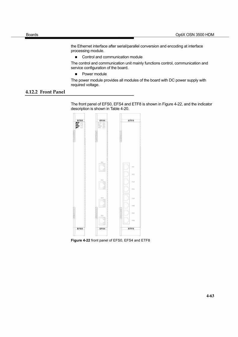
Boards OptiX OSN 3500 HDM
4-63
the Ethernet interface after serial/parallel conversion and encoding at interface processing module.
Control and communication module The control and communication unit mainly functions control, communication and service configuration of the board.
Power module The power module provides all modules of the board with DC power supply with required voltage.
4.12.2 Front Panel
The front panel of EFS0, EFS4 and ETF8 is shown in Figure 4-22, and the indicator description is shown in Table 4-20.
Figure 4-22 front panel of EFS0, EFS4 and ETF8
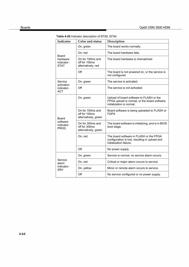
Boards OptiX OSN 3500 HDM
4-64
Table 4-20 Indicator description of EFS0, EFS4
Indicator Color and status Description On, green The board works normally.
On, red The board hardware fails.
On for 100ms and off for 100ms alternatively, red
The board hardware is mismatched. Board hardware indicator- STAT
Off The board is not powered on, or the service is not configured.
On, green The service is activated. Service activation indicator- ACT
Off The service is not activated.
On, green Upload of board software to FLASH or the FPGA upload is normal, or the board software initialization is normal.
On for 100ms and off for 100ms alternatively, green
Board software is being uploaded to FLASH or FGPA
On for 300ms and off for 300ms alternatively, green
The board software is initializing, and is in BIOS boot stage.
On, red The board software in FLASH or the FPGA configuration is lost, resulting in upload and initialization failure.
Board software indicator- PROG
Off No power supply.
On, green Service is normal, no service alarm occurs.
On, red Critical or major alarm occurs to service.
On, yellow Minor or remote alarm occurs to service.
Service alarm indicator- SRV
Off No service configured or no power supply.
Boards OptiX OSN 3500 HDM
4-65
4.12.3 Interface
EFS4 provides 4 Ethernet ports, and ETF8 provides the EFS0 with 8 ports. Table 4-21 shows the ports characteristics. Table 4-21 Ethernet ports characteristics
Type RJ-45
Impedance 100Ω
Specifications IEEE 802.3-compliant
Line code Manchester coding (10M), MLT-3 or NRZI
Two indicators for each interface, their meanings shown in Table 4-22. Table 4-22 Meanings of LED indicators on RJ-45 connector
Color Meaning Silkscreen Description Green link LINK* On: link is established;
Off: no link is established.
Orange activity ACT* Flash: there are data transmitted/received; Off: there is no data transmitted/received.
4.12.4 DIP Switch and Jumper
None
4.12.5 Board Configuration
Before using EFS4 or EFS0 for running service, parameters should be set for it through NM. Configuration should be provided to the following bytes:
J1 J1 is the path trace byte.Successive transmission of the higher order access point identifier through J1 at the transmit end helps the receive end learn that its connection with the specified transmit end is in continuous connection status. When J1 mismatch is detected at receive end, the corresponding VC-4 path will generate HP-TIM alarm.
C2 C2 is the signal label byte, indicating the multiplexing structure of VC-4 frame and the payload property. It is required that the C2 bytes transmitted match those received. Once mismatch is detected, the corresponding VC-4 path will generate HP-SLM alarm and insert all “1”s into the C4 in downstream stations.
Ethernet port working mode The Ethernet ports of the interconnected equipments are generally required to work in
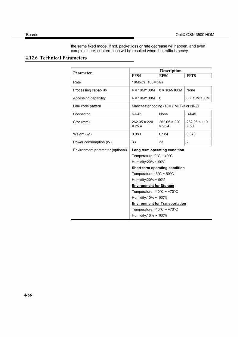
Boards OptiX OSN 3500 HDM
4-66
the same fixed mode. If not, packet loss or rate decrease will happen, and even complete service interruption will be resulted when the traffic is heavy.
4.12.6 Technical Parameters
Description Parameter EFS4 EFS0 EFT8
Rate 10Mbit/s, 100Mbit/s
Processing capability 4 × 10M/100M 8 × 10M/100M None
Accessing capability 4 × 10M/100M 0 8 × 10M/100M
Line code pattern Manchester coding (10M), MLT-3 or NRZI
Connector RJ-45 None RJ-45
Size (mm) 262.05 × 220 × 25.4
262.05 × 220 × 25.4
262.05 × 110 × 50
Weight (kg) 0.980 0.984 0.370
Power consumption (W) 33 33 2
Environment parameter (optional) Long term operating condition Temperature: 0°C ~ 40°C Humidity:20% ~ 90% Short term operating condition Temperature: -5°C ~ 50°C Humidity:20% ~ 90% Environment for Storage Temperature: -40°C ~ +70°C Humidity:10% ~ 100% Environment for Transportation Temperature: -40°C ~ +70°C Humidity:10% ~ 100%
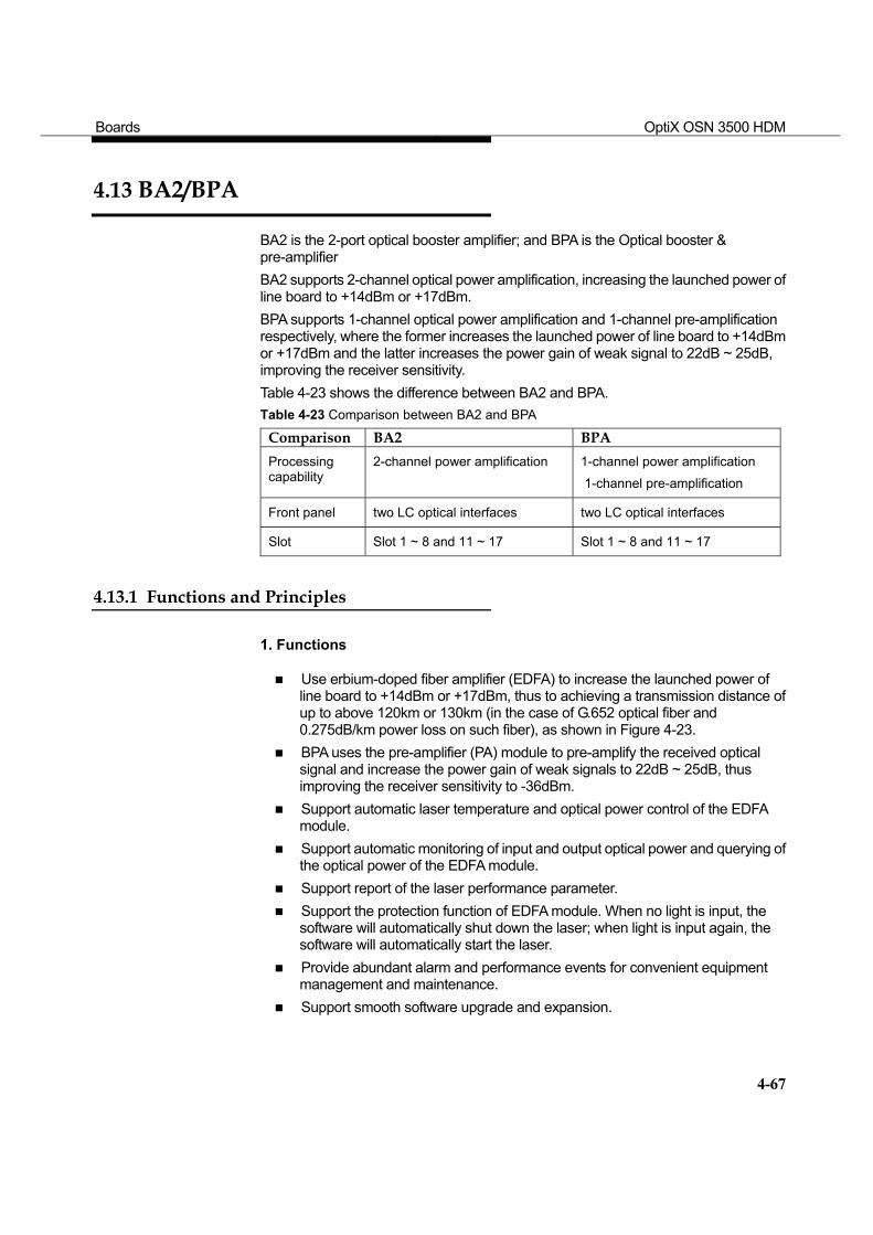
Boards OptiX OSN 3500 HDM
4-67
4.13 BA2/BPA
BA2 is the 2-port optical booster amplifier; and BPA is the Optical booster & pre-amplifier BA2 supports 2-channel optical power amplification, increasing the launched power of line board to +14dBm or +17dBm. BPA supports 1-channel optical power amplification and 1-channel pre-amplification respectively, where the former increases the launched power of line board to +14dBm or +17dBm and the latter increases the power gain of weak signal to 22dB ~ 25dB, improving the receiver sensitivity. Table 4-23 shows the difference between BA2 and BPA. Table 4-23 Comparison between BA2 and BPA
Comparison BA2 BPA Processing capability
2-channel power amplification 1-channel power amplification 1-channel pre-amplification
Front panel two LC optical interfaces two LC optical interfaces
Slot Slot 1 ~ 8 and 11 ~ 17 Slot 1 ~ 8 and 11 ~ 17
4.13.1 Functions and Principles
1. Functions
Use erbium-doped fiber amplifier (EDFA) to increase the launched power of line board to +14dBm or +17dBm, thus to achieving a transmission distance of up to above 120km or 130km (in the case of G.652 optical fiber and 0.275dB/km power loss on such fiber), as shown in Figure 4-23.
BPA uses the pre-amplifier (PA) module to pre-amplify the received optical signal and increase the power gain of weak signals to 22dB ~ 25dB, thus improving the receiver sensitivity to -36dBm.
Support automatic laser temperature and optical power control of the EDFA module.
Support automatic monitoring of input and output optical power and querying of the optical power of the EDFA module.
Support report of the laser performance parameter. Support the protection function of EDFA module. When no light is input, the
software will automatically shut down the laser; when light is input again, the software will automatically start the laser.
Provide abundant alarm and performance events for convenient equipment management and maintenance.
Support smooth software upgrade and expansion.
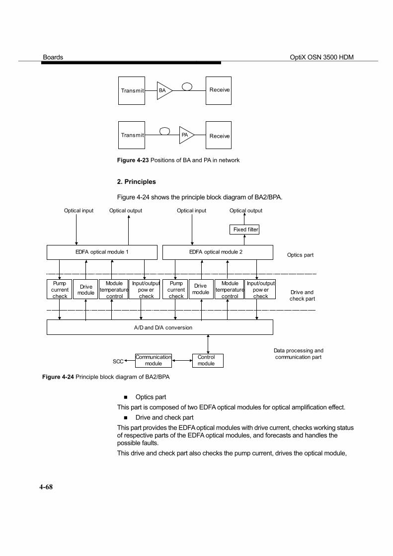
Boards OptiX OSN 3500 HDM
4-68
BA
PA Receive
Transmit
Transmit
Receive
Figure 4-23 Positions of BA and PA in network
2. Principles
Figure 4-24 shows the principle block diagram of BA2/BPA.
Optical outputOptical input Optical input Optical output
Optics part
Fixed f ilter
Drivemodule
Drivemodule
SCCControlmodule
Communicationmodule
A/D and D/A conversion
Pumpcurrentcheck
Drive andcheck part
Data processing andcommunication part
Pumpcurrentcheck
Moduletemperature
control
Moduletemperature
control
Input/outputpow ercheck
EDFA optical module 1 EDFA optical module 2
Input/outputpow ercheck
Figure 4-24 Principle block diagram of BA2/BPA
Optics part
This part is composed of two EDFA optical modules for optical amplification effect. Drive and check part
This part provides the EDFA optical modules with drive current, checks working status of respective parts of the EDFA optical modules, and forecasts and handles the possible faults. This drive and check part also checks the pump current, drives the optical module,
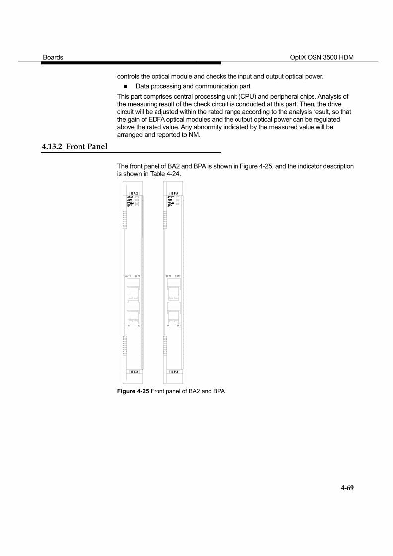
Boards OptiX OSN 3500 HDM
4-69
controls the optical module and checks the input and output optical power. Data processing and communication part
This part comprises central processing unit (CPU) and peripheral chips. Analysis of the measuring result of the check circuit is conducted at this part. Then, the drive circuit will be adjusted within the rated range according to the analysis result, so that the gain of EDFA optical modules and the output optical power can be regulated above the rated value. Any abnormity indicated by the measured value will be arranged and reported to NM.
4.13.2 Front Panel
The front panel of BA2 and BPA is shown in Figure 4-25, and the indicator description is shown in Table 4-24.
Figure 4-25 Front panel of BA2 and BPA

Boards OptiX OSN 3500 HDM
4-70
Table 4-24 Indicator description of BA2 and BPA
Indicator Color and status Description On, green The board works normally.
On, red The board hardware fails.
On for 100ms and off for 100ms alternatively, red
The board hardware is mismatched.
Board hardware indicator- STAT
Off The board is not powered on.
On, green The service is activated, and the board is in service. Specifically, the board is in working status and the service is active in TPS mode;and the indicator is normally on in the case of no TPS provided.
Service activation indicator-ACT
Off The service is not activated, and the board can be swapped.
On, green Upload of board software to FLASH or the FPGA upload is normal, or the board software initialization is normal.
On for 100ms and off for 100ms alternatively, green
Board software is being uploaded to FLASH or FGPA
On for 300ms and off for 300ms alternatively, green
The board software is initializing, and is in BIOS boot stage.
On, red The board software in FLASH or the FPGA configuration is lost, resulting in upload and initialization failure.
Board software indicator- PROG
Off No power supply.
On, green Service is normal, no service alarm occurs.
On, red Critical or major alarm occurs to service.
On, yellow Minor or remote alarm occurs to service.
Service alarm indicator-SRV
Off No service is configured.
Boards OptiX OSN 3500 HDM
4-71
4.13.3 Interface
Interface description for BA2 and BPA is shown in Table 4-25. Table 4-25 Interface description for BA2 and BPA
Item BA2 BPA Input wavelength BA: 1530 ~ 1565nm BA: 1530 ~ 1565nm
PA: 1550.12nm
Input optical power range BA: -6 ~ +3dBm BA: -6 ~ +3dBm PA: -10 ~ -36dBm
Output optical power BA: +14dBm or +17dBm BA: +14dBm or +17dBm
Sensitivity - PA: -36dBm
Noise figure <6.5dB BA: <6.5dB PA: <6dB
Optical interface supported
V-16.2, U-16.2, L-64.2, V-64.2 and U-64.2
V-16.2, U-16.2, L-64.2, V-64.2 and U-64.2
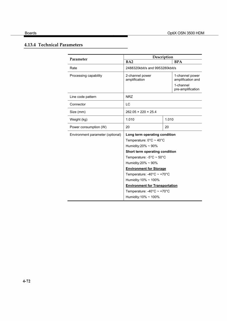
Boards OptiX OSN 3500 HDM
4-72
4.13.4 Technical Parameters
Description Parameter BA2 BPA
Rate 2488320kbit/s and 9953280kbit/s
Processing capability 2-channel power amplification
1-channel power amplification and 1-channel pre-amplification
Line code pattern NRZ
Connector LC
Size (mm) 262.05 × 220 × 25.4
Weight (kg) 1.010 1.010
Power consumption (W) 20 20
Environment parameter (optional) Long term operating condition Temperature: 0°C ~ 40°C Humidity:20% ~ 90% Short term operating condition Temperature: -5°C ~ 50°C Humidity:20% ~ 90% Environment for Storage Temperature: -40°C ~ +70°C Humidity:10% ~ 100% Environment for Transportation Temperature: -40°C ~ +70°C Humidity:10% ~ 100%
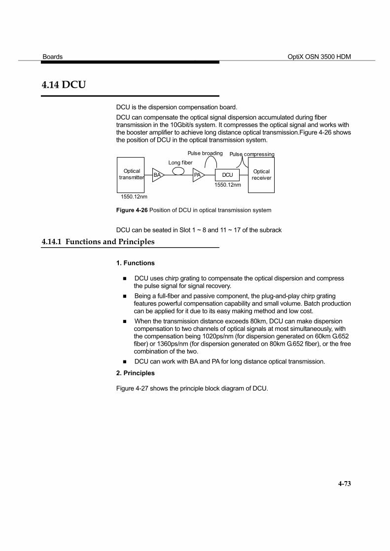
Boards OptiX OSN 3500 HDM
4-73
4.14 DCU
DCU is the dispersion compensation board. DCU can compensate the optical signal dispersion accumulated during fiber transmission in the 10Gbit/s system. It compresses the optical signal and works with the booster amplifier to achieve long distance optical transmission.Figure 4-26 shows the position of DCU in the optical transmission system.
BA PA DCU
1550.12nm
1550.12nm
Pulse compressingLong fiber
Opticaltransmitter
Opticalreceiver
Pulse broading
Figure 4-26 Position of DCU in optical transmission system DCU can be seated in Slot 1 ~ 8 and 11 ~ 17 of the subrack
4.14.1 Functions and Principles
1. Functions
DCU uses chirp grating to compensate the optical dispersion and compress the pulse signal for signal recovery.
Being a full-fiber and passive component, the plug-and-play chirp grating features powerful compensation capability and small volume. Batch production can be applied for it due to its easy making method and low cost.
When the transmission distance exceeds 80km, DCU can make dispersion compensation to two channels of optical signals at most simultaneously, with the compensation being 1020ps/nm (for dispersion generated on 60km G.652 fiber) or 1360ps/nm (for dispersion generated on 80km G.652 fiber), or the free combination of the two.
DCU can work with BA and PA for long distance optical transmission.
2. Principles
Figure 4-27 shows the principle block diagram of DCU.
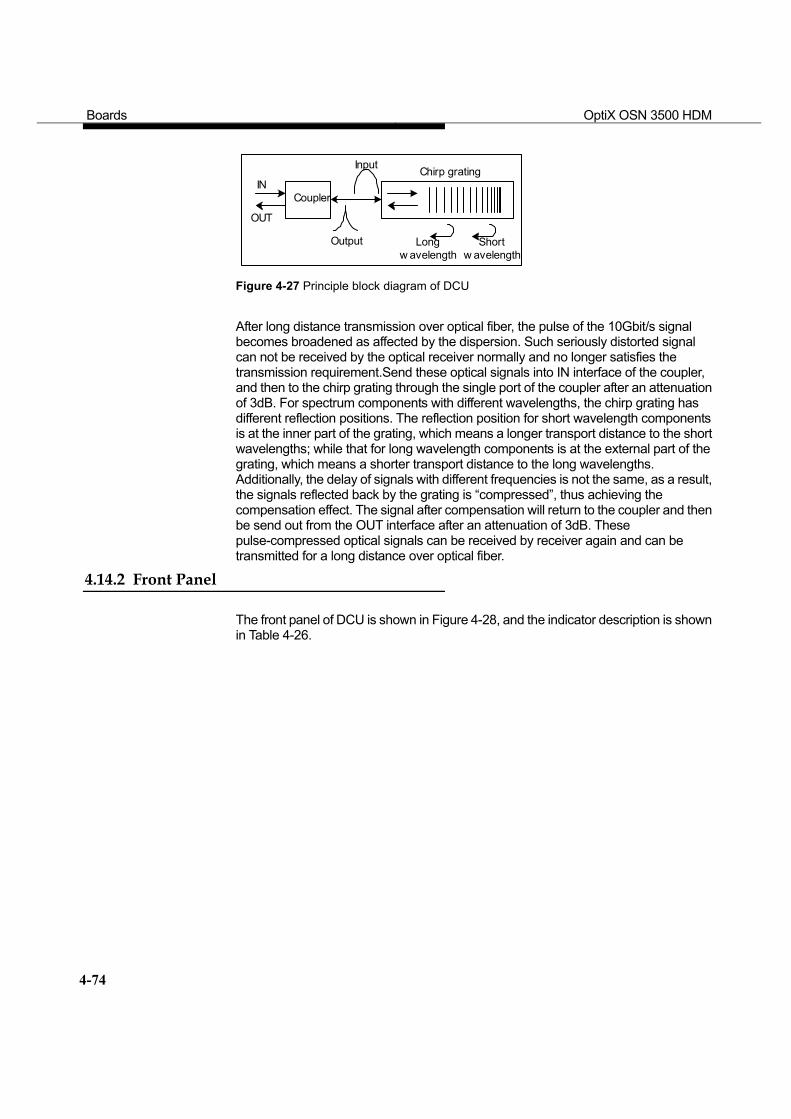
Boards OptiX OSN 3500 HDM
4-74
IN
OUT
Coupler
Chirp grating
Longw avelength
Shortw avelength
Input
Output
Figure 4-27 Principle block diagram of DCU After long distance transmission over optical fiber, the pulse of the 10Gbit/s signal becomes broadened as affected by the dispersion. Such seriously distorted signal can not be received by the optical receiver normally and no longer satisfies the transmission requirement.Send these optical signals into IN interface of the coupler, and then to the chirp grating through the single port of the coupler after an attenuation of 3dB. For spectrum components with different wavelengths, the chirp grating has different reflection positions. The reflection position for short wavelength components is at the inner part of the grating, which means a longer transport distance to the short wavelengths; while that for long wavelength components is at the external part of the grating, which means a shorter transport distance to the long wavelengths. Additionally, the delay of signals with different frequencies is not the same, as a result, the signals reflected back by the grating is “compressed”, thus achieving the compensation effect. The signal after compensation will return to the coupler and then be send out from the OUT interface after an attenuation of 3dB. These pulse-compressed optical signals can be received by receiver again and can be transmitted for a long distance over optical fiber.
4.14.2 Front Panel
The front panel of DCU is shown in Figure 4-28, and the indicator description is shown in Table 4-26.
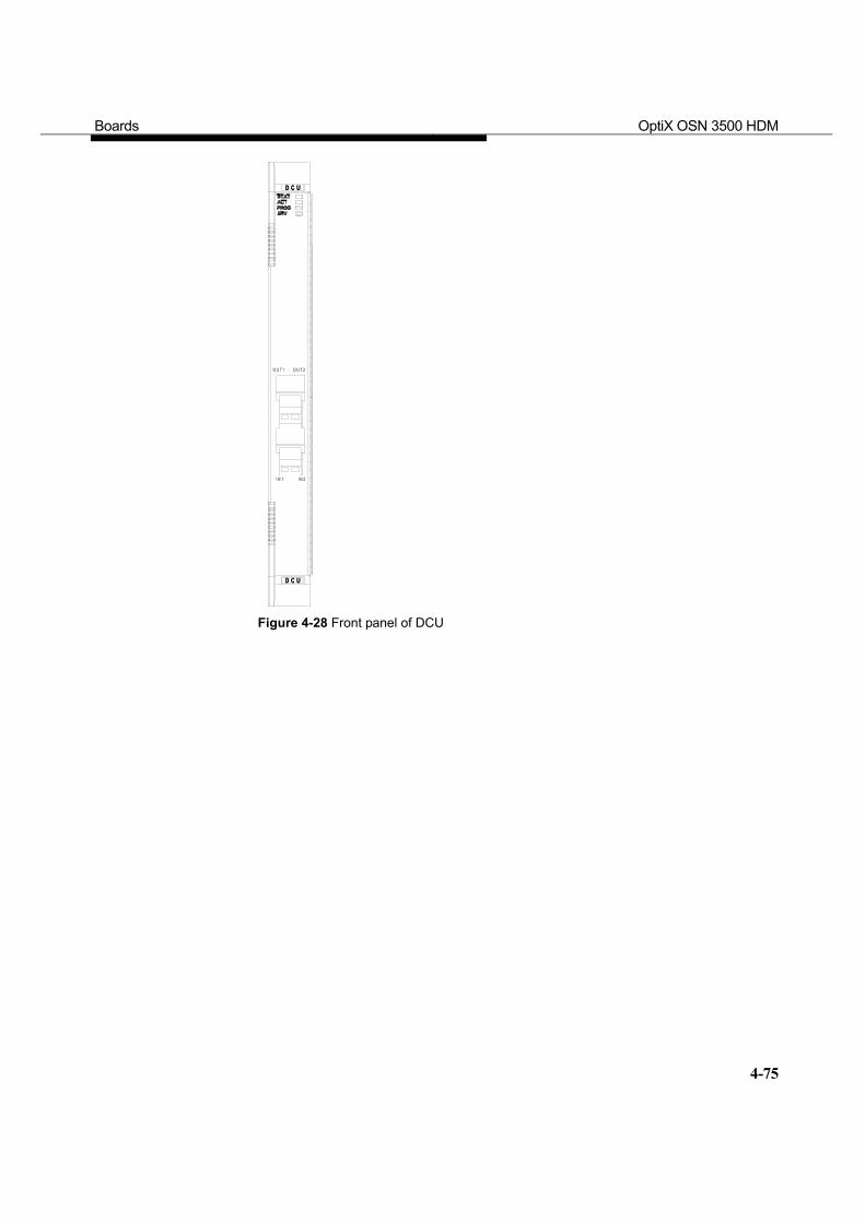
Boards OptiX OSN 3500 HDM
4-75
Figure 4-28 Front panel of DCU

Boards OptiX OSN 3500 HDM
4-76
Table 4-26 Indicator description of DCU
Indicator Color and status Description On, green The board works normally.
On, red The board hardware fails.
On for 100ms and off for 100ms alternatively, red
The board hardware is mismatched.
Board hardware indicator- STAT
Off The board is not powered on.
On, green The service is activated, and the board is in service. Specifically, the board is in working status and the service is active in TPS mode;and the indicator is normally on in the case of no TPS provided.
Service activation indicator-ACT
Off The service is not activated, and the board can be swapped.
On, green Upload of board software to FLASH or the FPGA upload is normal, or the board software initialization is normal.
On for 100ms and off for 100ms alternatively, green
Board software is being uploaded to FLASH or FGPA
On for 300ms and off for 300ms alternatively, green
The board software is initializing, and is in BIOS boot stage.
On, red The board software in FLASH or the FPGA configuration is lost, resulting in upload and initialization failure.
Board software indicator- PROG
Off No power supply.
On, green Service is normal, no service alarm occurs.
On, red Critical or major alarm occurs to service.
On, yellow Minor or remote alarm occurs to service.
Service alarm indicator-SRV
Off No service is configured.
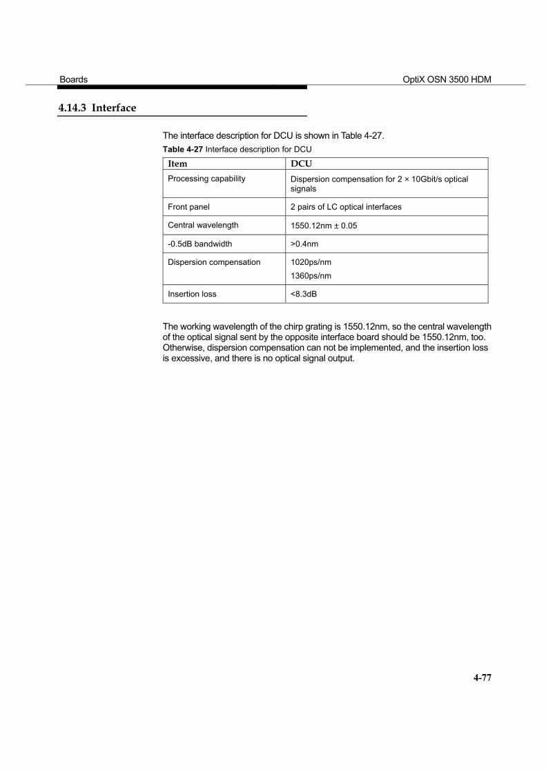
Boards OptiX OSN 3500 HDM
4-77
4.14.3 Interface
The interface description for DCU is shown in Table 4-27. Table 4-27 Interface description for DCU
Item DCU Processing capability Dispersion compensation for 2 × 10Gbit/s optical
signals
Front panel 2 pairs of LC optical interfaces
Central wavelength 1550.12nm ± 0.05
-0.5dB bandwidth >0.4nm
Dispersion compensation 1020ps/nm 1360ps/nm
Insertion loss <8.3dB
The working wavelength of the chirp grating is 1550.12nm, so the central wavelength of the optical signal sent by the opposite interface board should be 1550.12nm, too. Otherwise, dispersion compensation can not be implemented, and the insertion loss is excessive, and there is no optical signal output.
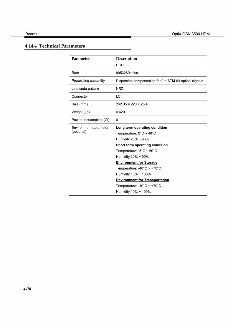
Boards OptiX OSN 3500 HDM
4-78
4.14.4 Technical Parameters
Parameter Description DCU
Rate 9953280kbit/s
Processing capability Dispersion compensation for 2 × STM-64 optical signals
Line code pattern NRZ
Connector LC
Size (mm) 262.05 × 220 × 25.4
Weight (kg) 0.420
Power consumption (W) 0
Environment parameter (optional)
Long term operating condition Temperature: 0°C ~ 40°C Humidity:20% ~ 90% Short term operating condition Temperature: -5°C ~ 50°C Humidity:20% ~ 90% Environment for Storage Temperature: -40°C ~ +70°C Humidity:10% ~ 100% Environment for Transportation Temperature: -40°C ~ +70°C Humidity:10% ~ 100%
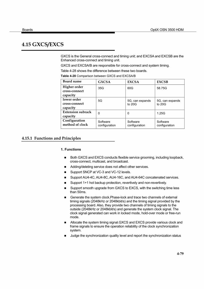
Boards OptiX OSN 3500 HDM
4-79
4.15 GXCS/EXCS
GXCS is the General cross-connect and timing unit; and EXCSA and EXCSB are the Enhanced cross-connect and timing unit. GXCS and EXCSA/B are responsible for cross-connect and system timing. Table 4-28 shows the difference between these two boards. Table 4-28 Comparison between GXCS and EXCSA/B
Board name GXCSA EXCSA EXCSB Higher order cross-connect capacity
35G 60G 58.75G
lower order cross-connect capacity
5G 5G, can expands to 20G
5G, can expands to 20G
Extension subrack capacity
0 0 1.25G
Configuration method of clock
Software configuration
Software configuration
Software configuration
4.15.1 Functions and Principles
1. Functions
Both GXCS and EXCS conducts flexible service grooming, including loopback, cross-connect, multicast, and broadcast.
Adding/deleting service does not affect other services. Support SNCP at VC-3 and VC-12 levels. Support AU4-4C, AU4-8C, AU4-16C, and AU4-64C concatenated services. Support 1+1 hot backup protection, revertively and non-revertively. Support smooth upgrade from GXCS to EXCS, with the switching time less
than 50ms. Generate the system clock.Phase-lock and trace two channels of external
timing signals (2048kHz or 2048kbit/s) and the timing signal provided by the processing board. Also, they provide two channels of timing signals to the outside (2048kHz or 2048kbit/s) and generate the system clock signal. The clock signal generated can work in locked mode, hold-over mode or free-run mode.
Allocate the system timing signal.GXCS and EXCS provide various clock and frame signals to ensure the operation reliability of the clock synchronization system.
Judge the synchronization quality level and report the synchronization status
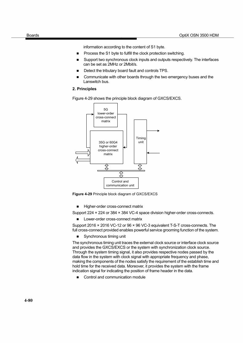
Boards OptiX OSN 3500 HDM
4-80
information according to the content of S1 byte. Process the S1 byte to fulfill the clock protection switching. Support two synchronous clock inputs and outputs respectively. The interfaces
can be set as 2MHz or 2Mbit/s. Detect the tributary board fault and controls TPS. Communicate with other boards through the two emergency buses and the
Lanswitch bus.
2. Principles
Figure 4-29 shows the principle block diagram of GXCS/EXCS.
5Glower-order
cross-connectmatrix
35G or 60G4higher-order
cross-connectmatrix
Timingunit
Control andcommunication unit
Figure 4-29 Principle block diagram of GXCS/EXCS
Higher-order cross-connect matrix Support 224 × 224 or 384 × 384 VC-4 space division higher-order cross-connects.
Lower-order cross-connect matrix Support 2016 × 2016 VC-12 or 96 × 96 VC-3 equivalent T-S-T cross-connects. The full cross-connect provided enables powerful service grooming function of the system.
Synchronous timing unit The synchronous timing unit traces the external clock source or interface clock source and provides the GXCS/EXCS or the system with synchronization clock source. Through the system timing signal, it also provides respective nodes passed by the data flow in the system with clock signal with appropriate frequency and phase, making the components of the nodes satisfy the requirement of the establish time and hold time for the received data. Moreover, it provides the system with the frame indication signal for indicating the position of frame header in the data.
Control and communication module
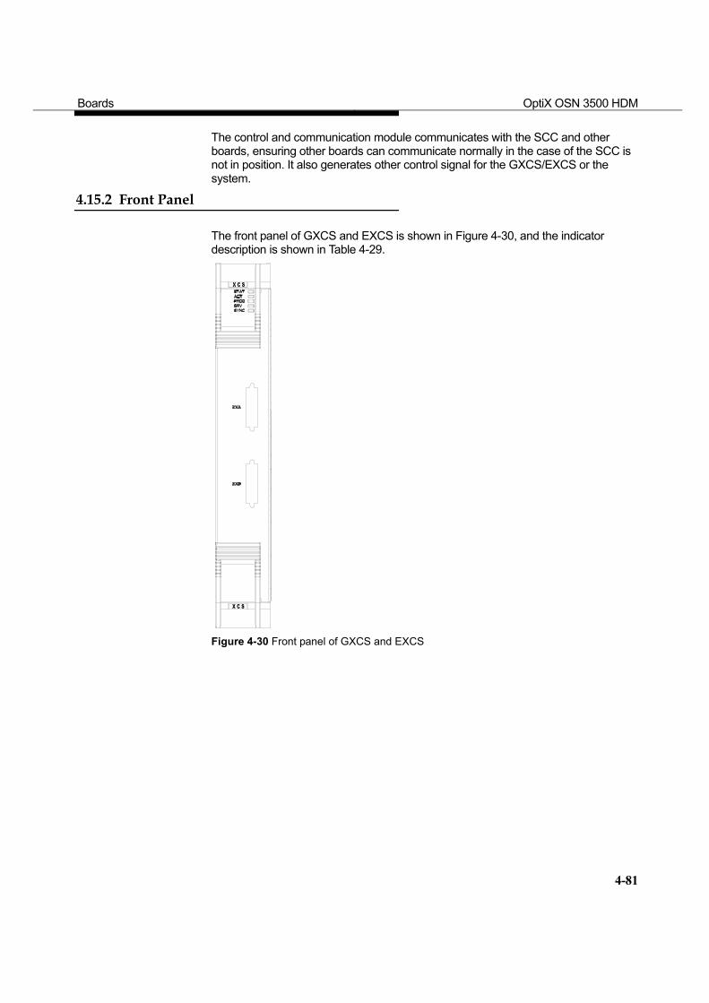
Boards OptiX OSN 3500 HDM
4-81
The control and communication module communicates with the SCC and other boards, ensuring other boards can communicate normally in the case of the SCC is not in position. It also generates other control signal for the GXCS/EXCS or the system.
4.15.2 Front Panel
The front panel of GXCS and EXCS is shown in Figure 4-30, and the indicator description is shown in Table 4-29.
Figure 4-30 Front panel of GXCS and EXCS
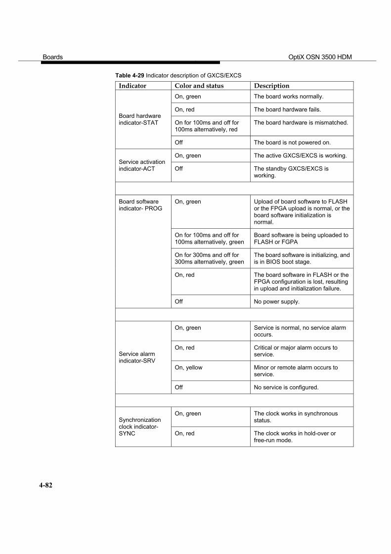
Boards OptiX OSN 3500 HDM
4-82
Table 4-29 Indicator description of GXCS/EXCS
Indicator Color and status Description On, green The board works normally.
On, red The board hardware fails.
On for 100ms and off for 100ms alternatively, red
The board hardware is mismatched.Board hardware indicator-STAT
Off The board is not powered on.
On, green The active GXCS/EXCS is working. Service activation indicator-ACT Off The standby GXCS/EXCS is
working.
On, green Upload of board software to FLASH or the FPGA upload is normal, or the board software initialization is normal.
On for 100ms and off for 100ms alternatively, green
Board software is being uploaded to FLASH or FGPA
On for 300ms and off for 300ms alternatively, green
The board software is initializing, and is in BIOS boot stage.
On, red The board software in FLASH or the FPGA configuration is lost, resulting in upload and initialization failure.
Board software indicator- PROG
Off No power supply.
On, green Service is normal, no service alarm occurs.
On, red Critical or major alarm occurs to service.
On, yellow Minor or remote alarm occurs to service.
Service alarm indicator-SRV
Off No service is configured.
On, green The clock works in synchronous status. Synchronization
clock indicator- SYNC On, red The clock works in hold-over or
free-run mode.
Boards OptiX OSN 3500 HDM
4-83
4.15.3 Interface
GXCS/EXCS has four external clock interfaces, two for input and two for output. Types of the input/output clock signal fall into 2Mbit/s and 2MHz. The input/output interfaces, four 75Ω SMB clock interfaces and two 120Ω RJ-45 interfaces, are on the AUX board.
4.15.4 DIP Switch and Jumper
None
4.15.5 Board Configuration
Before the GXCS/EXCS is put into operation, configuration must be provided to the following parameters through NM.
1. Clock parameter
In common application where there is neither external clock input and output nor requirement for S1 byte for clock switching protection, the configuration for the synchronous timing unit is simple. Only the following configurations are needed:
Reference clock source Clock source stratum
When the reference clock source is the external BITS clock and the clock protection switching is required, the configuration is relatively complicated. The following configurations are required:
Reference clock source Clock source stratum External BITS type S1 byte Threshold of triggering clock switching protection
These configuration items in the NM operating system are explained below.
(1) Clock source stratum
It refers to the stratums of all available reference clock sources of the synchronous timing unit. In normal working state, the synchronous timing unit uses the clock source of the highest stratum as its reference clock. In case the clock source of higher stratum is lost, the one with lower stratum will be used instead, and so on and so forth, till the clock source of the lowest stratum is used ultimately. Generally the internal clock source is taken as the clock of the lowest stratum. So, when all the available clock sources are lost, the synchronous timing unit will eventually work in the free-run mode.
(2) Synchronous source
It is the current synchronous clock source configured for the synchronous timing unit. It must be one listed in the clock sources list. The clock of the highest class is usually
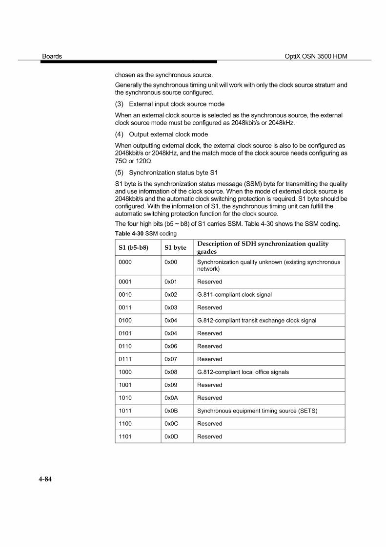
Boards OptiX OSN 3500 HDM
4-84
chosen as the synchronous source. Generally the synchronous timing unit will work with only the clock source stratum and the synchronous source configured.
(3) External input clock source mode
When an external clock source is selected as the synchronous source, the external clock source mode must be configured as 2048kbit/s or 2048kHz.
(4) Output external clock mode
When outputting external clock, the external clock source is also to be configured as 2048kbit/s or 2048kHz, and the match mode of the clock source needs configuring as 75Ω or 120Ω.
(5) Synchronization status byte S1
S1 byte is the synchronization status message (SSM) byte for transmitting the quality and use information of the clock source. When the mode of external clock source is 2048kbit/s and the automatic clock switching protection is required, S1 byte should be configured. With the information of S1, the synchronous timing unit can fulfill the automatic switching protection function for the clock source. The four high bits (b5 ~ b8) of S1 carries SSM. Table 4-30 shows the SSM coding. Table 4-30 SSM coding
S1 (b5-b8) S1 byte Description of SDH synchronization quality grades
0000 0x00 Synchronization quality unknown (existing synchronous network)
0001 0x01 Reserved
0010 0x02 G.811-compliant clock signal
0011 0x03 Reserved
0100 0x04 G.812-compliant transit exchange clock signal
0101 0x04 Reserved
0110 0x06 Reserved
0111 0x07 Reserved
1000 0x08 G.812-compliant local office signals
1001 0x09 Reserved
1010 0x0A Reserved
1011 0x0B Synchronous equipment timing source (SETS)
1100 0x0C Reserved
1101 0x0D Reserved
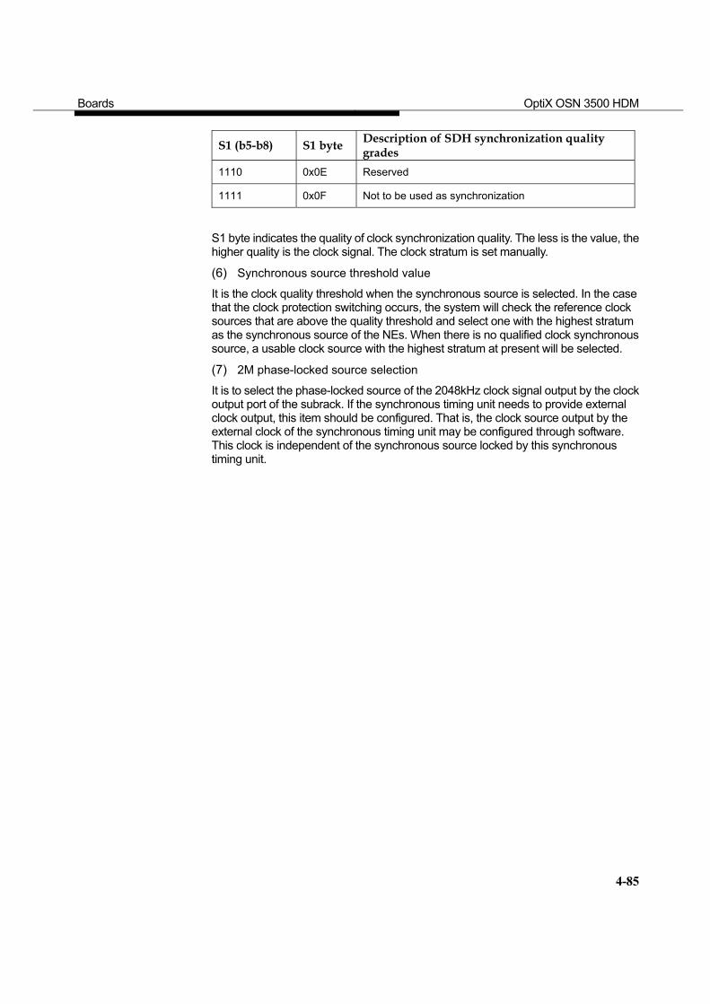
Boards OptiX OSN 3500 HDM
4-85
S1 (b5-b8) S1 byte Description of SDH synchronization quality grades
1110 0x0E Reserved
1111 0x0F Not to be used as synchronization
S1 byte indicates the quality of clock synchronization quality. The less is the value, the higher quality is the clock signal. The clock stratum is set manually.
(6) Synchronous source threshold value
It is the clock quality threshold when the synchronous source is selected. In the case that the clock protection switching occurs, the system will check the reference clock sources that are above the quality threshold and select one with the highest stratum as the synchronous source of the NEs. When there is no qualified clock synchronous source, a usable clock source with the highest stratum at present will be selected.
(7) 2M phase-locked source selection
It is to select the phase-locked source of the 2048kHz clock signal output by the clock output port of the subrack. If the synchronous timing unit needs to provide external clock output, this item should be configured. That is, the clock source output by the external clock of the synchronous timing unit may be configured through software. This clock is independent of the synchronous source locked by this synchronous timing unit.
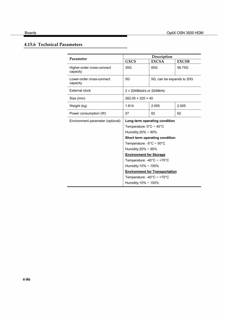
Boards OptiX OSN 3500 HDM
4-86
4.15.6 Technical Parameters
Description Parameter GXCS EXCSA EXCSB
Higher-order cross-connect capacity
35G 60G 58.75G
Lower-order cross-connect capacity
5G 5G, can be expands to 20G
External clock 2 × 2048kbit/s or 2048kHz
Size (mm) 262.05 × 220 × 40
Weight (kg) 1.814 2.005 2.005
Power consumption (W) 27 62 62
Environment parameter (optional) Long term operating condition Temperature: 0°C ~ 40°C Humidity:20% ~ 90% Short term operating condition Temperature: -5°C ~ 50°C Humidity:20% ~ 90% Environment for Storage Temperature: -40°C ~ +70°C Humidity:10% ~ 100% Environment for Transportation Temperature: -40°C ~ +70°C Humidity:10% ~ 100%
Boards OptiX OSN 3500 HDM
4-87
4.16 SCC
SCC is the system control and communication board. It functions main control, orderwire, communication and system power monitoring.
4.16.1 Functions and Principles
1. Functions
Support 1+1 hot backup protection. When the active board fails, the service will be switched to the standby board automatically.
Configure and groom service, monitor service performance, and collect performance event and alarm information.
Provide 10M and 100M compatible Ethernet NM interface. Provide F&f interface through the AUX board for tone & data access unit (TDA),
case-shape optical amplifier (COA) and DCU management. Provide two 4M HDLC emergency paths for inter-board communication as well
as MSP and SNCP. Provide one 10M/100M Ethernet interface for connection with the Lanswitch
module of AUX to support the communication between various boards in the system.
Provide one 10M Ethernet interface for communication between the active and standby SCCs.
Process fifty data communication channels (DCCs) (D1 ~ D3) to provide the transmit link for network management.
Process such bytes as E1, E2, F1 and Serial 1 ~ 4. Provide one 64k codirectional data interface F1 through AUX. Provide the operation administration and maintenance (OAM) interface
through AUX, supporting remote maintenance of the Modem of RS232 data connected equipment (DCE).
Monitor the two -48V power supplies of the system. Support four cabinet indicators. Process sixteen Boolean inputs and four Boolean outputs. Monitor the 3.3V power alarm of AUX. Support fan alarm and management function. Provide PIU with lightening protection and in-position detection function.
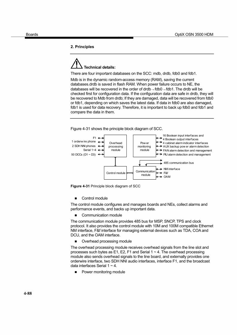
Boards OptiX OSN 3500 HDM
4-88
2. Principles
Technical details: There are four important databases on the SCC: mdb, drdb, fdb0 and fdb1. Mdb is in the dynamic random-access memory (RAM), saving the current databases.drdb is saved in flash RAM. When power failure occurs to NE, the databases will be recovered in the order of drdb→fdb0→fdb1. The drdb will be checked first for configuration data. If the configuration data are safe in drdb, they will be recovered to Mdb from drdb; If they are damaged, data will be recovered from fdb0 or fdb1, depending on which saves the latest data. If data in fdb0 are also damaged, fdb1 is used for data recovery. Therefore, it is important to back up fdb0 and fdb1 and compare the data in them.
Figure 4-31 shows the principle block diagram of SCC.
Serial 1~4
F1
F&fOAM
50 DCCs (D1 ~ D3)
Pow ermonitoring
module
1 orderw ire phone 4 cabinet alarm indicator interfacesAUX backup pow er alarm detectionFAN alarm detection and managementPIU alarm detection and management
485 communication bus
NM interfaceControl module Communication
module
Overheadprocessing
module
16 Boolean input interfaces and4 Boolean output interfaces
2 SDH NNI phones
Figure 4-31 Principle block diagram of SCC
Control module The control module configures and manages boards and NEs, collect alarms and performance events, and backs up important data.
Communication module The communication module provides 485 bus for MSP, SNCP, TPS and clock protocol. It also provides the control module with 10M and 100M compatible Ethernet NM interface, F&f interface for managing external devices such as TDA, COA and DCU, and the OAM interface.
Overhead processing module The overhead processing module receives overhead signals from the line slot and processes such bytes as E1, E2, F1 and Serial 1 ~ 4. The overhead processing module also sends overhead signals to the line board, and externally provides one orderwire interface, two SDH NNI audio interfaces, interface F1, and the broadcast data interfaces Serial 1 ~ 4.
Power monitoring module
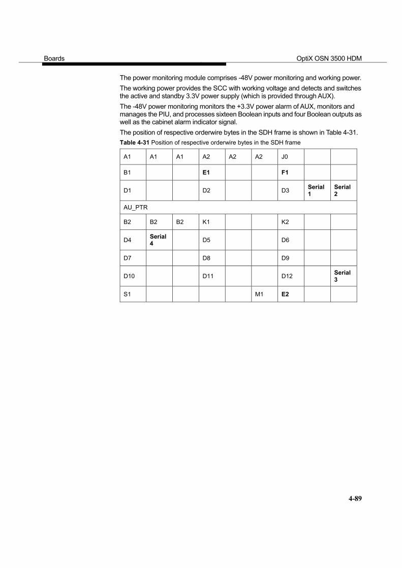
Boards OptiX OSN 3500 HDM
4-89
The power monitoring module comprises -48V power monitoring and working power. The working power provides the SCC with working voltage and detects and switches the active and standby 3.3V power supply (which is provided through AUX). The -48V power monitoring monitors the +3.3V power alarm of AUX, monitors and manages the PIU, and processes sixteen Boolean inputs and four Boolean outputs as well as the cabinet alarm indicator signal. The position of respective orderwire bytes in the SDH frame is shown in Table 4-31. Table 4-31 Position of respective orderwire bytes in the SDH frame
A1 A1 A1 A2 A2 A2 J0
B1 E1 F1
D1 D2 D3 Serial 1
Serial 2
AU_PTR
B2 B2 B2 K1 K2
D4 Serial4 D5 D6
D7 D8 D9
D10 D11 D12 Serial3
S1 M1 E2
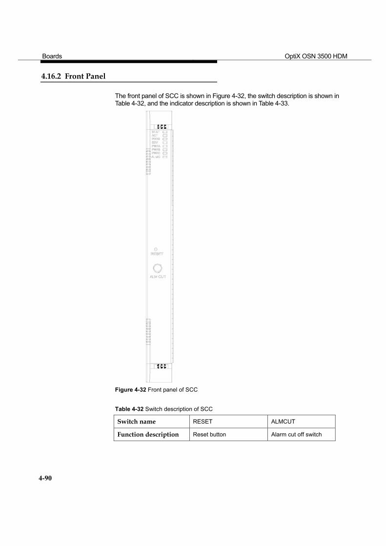
Boards OptiX OSN 3500 HDM
4-90
4.16.2 Front Panel
The front panel of SCC is shown in Figure 4-32, the switch description is shown in Table 4-32, and the indicator description is shown in Table 4-33.
Figure 4-32 Front panel of SCC Table 4-32 Switch description of SCC
Switch name RESET ALMCUT
Function description Reset button Alarm cut off switch
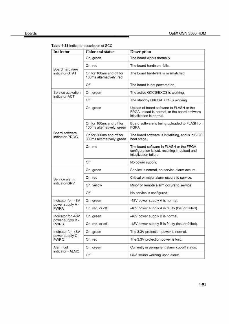
Boards OptiX OSN 3500 HDM
4-91
Table 4-33 Indicator description of SCC
Indicator Color and status Description On, green The board works normally.
On, red The board hardware fails.
On for 100ms and off for 100ms alternatively, red
The board hardware is mismatched. Board hardware indicator-STAT
Off The board is not powered on.
On, green The active GXCS/EXCS is working. Service activation indicator-ACT
Off The standby GXCS/EXCS is working.
On, green Upload of board software to FLASH or the FPGA upload is normal, or the board software initialization is normal.
On for 100ms and off for 100ms alternatively, green
Board software is being uploaded to FLASH or FGPA
On for 300ms and off for 300ms alternatively, green
The board software is initializing, and is in BIOS boot stage.
On, red The board software in FLASH or the FPGA configuration is lost, resulting in upload and initialization failure.
Board software indicator-PROG
Off No power supply.
On, green Service is normal, no service alarm occurs.
On, red Critical or major alarm occurs to service.
On, yellow Minor or remote alarm occurs to service.
Service alarm indicator-SRV
Off No service is configured.
On, green -48V power supply A is normal. Indicator for -48V power supply A - PWRA On, red, or off -48V power supply A is faulty (lost or failed).
On, green -48V power supply B is normal. Indicator for -48V power supply B - PWRB On, red, or off -48V power supply B is faulty (lost or failed).
On, green The 3.3V protection power is normal. Indicator for -48V power supply C - PWRC On, red The 3.3V protection power is lost.
On, green Currently in permanent alarm cut-off status. Alarm cut indicator - ALMC
Off Give sound warning upon alarm.
Boards OptiX OSN 3500 HDM
4-92
4.16.3 Interface
Interfaces provided by SCC are led out through AUX, refer to “External interface description of AUX” for details.
4.16.4 Technical Parameters
Parameter Description Board name SCC
Processing capability System control, inter-board communication, orderwire, and power detection
Size (mm) 262.05 × 220 × 25.4
Weight (kg) 0.884
Power consumption (W) 10
Environment parameter (optional) Long term operating condition Temperature: 0°C ~ 40°C Humidity:20% ~ 90% Short term operating condition Temperature: -5°C ~ 50°C Humidity:20% ~ 90% Environment for Storage Temperature: -40°C ~ +70°C Humidity:10% ~ 100% Environment for Transportation Temperature: -40°C ~ +70°C Humidity:10% ~ 100%
Boards OptiX OSN 3500 HDM
4-93
4.17 AUX
AUX is the system auxiliary interface board, seated in Slot 37 of the subrack.
AUX provides the system with such interfaces as 10M/100M Lanswitch, F&f, OAM, orderwire, F1, clock input/output, and the central backup function of the +3.3V board power supply.
4.17.1 Functions and Principles
1. Functions
Provide X.25-supporting interface OAM. Provide sixteen Boolean input interfaces and four Boolean output interface. Provide four output alarm concatenation interfaces Provide four auxiliary serial data interfaces (Series 1 ~ 4) for data transparent
transmission. Provide one 64kbit/s codirectional data path interface (F1). Provide one orderwire interface.1. Provide two subnet outgoing audio interfaces. Provide three Ethernet NM interfaces, two connecting with the active and
standby SCCs and the other one with NM. Provide one 10M and 100M compatible Ethernet commissioning interface for
subrack commissioning. Provide one 10M and 100M compatible Ethernet interface; Support one
extension subrack and implement service configuration and grooming of the subrack.
Provide nineteen 10M and 100M compatible Ethernet interfaces for inter-board communication.
Provide two analog BITS clock input interfaces and two analog BITS clock output interfaces.
Provide two data BITS clock input interfaces and two data BITS clock output interfaces.
Provide administration serial interface F&f to manage such external devices as COA, TDA and DCU.
Support the central backup function of the board +3.3V power supply, that is, 1:N protection for the secondary power supply of the boards.
Provide the orderwire ring current function. Provide four cabinet indicators and support alarm concatenation.
2. Principles
Figure 4-33 shows the principle block diagram of AUX.
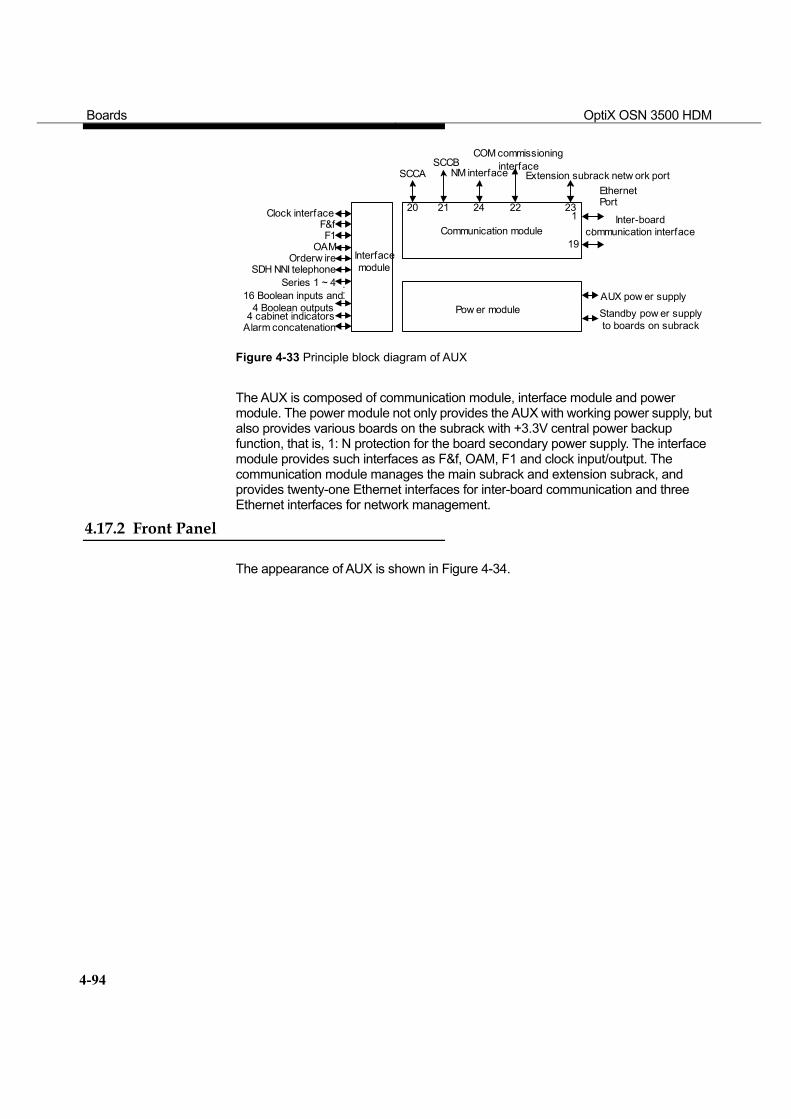
Boards OptiX OSN 3500 HDM
4-94
1
19
21 22 232420EthernetPort
SCCASCCB
...
...
F&fF1
OAM
NM interface
Clock interface
Orderw ire
Series 1 ~ 4
Alarm concatenation4 cabinet indicators
Communication module
Pow er module
Inter-boardcommunication interface
Interfacemodule
Standby pow er supplyto boards on subrack
COM commissioninginterface
Extension subrack netw ork port
SDH NNI telephone
AUX pow er supply16 Boolean inputs and4 Boolean outputs
Figure 4-33 Principle block diagram of AUX The AUX is composed of communication module, interface module and power module. The power module not only provides the AUX with working power supply, but also provides various boards on the subrack with +3.3V central power backup function, that is, 1: N protection for the board secondary power supply. The interface module provides such interfaces as F&f, OAM, F1 and clock input/output. The communication module manages the main subrack and extension subrack, and provides twenty-one Ethernet interfaces for inter-board communication and three Ethernet interfaces for network management.
4.17.2 Front Panel
The appearance of AUX is shown in Figure 4-34.
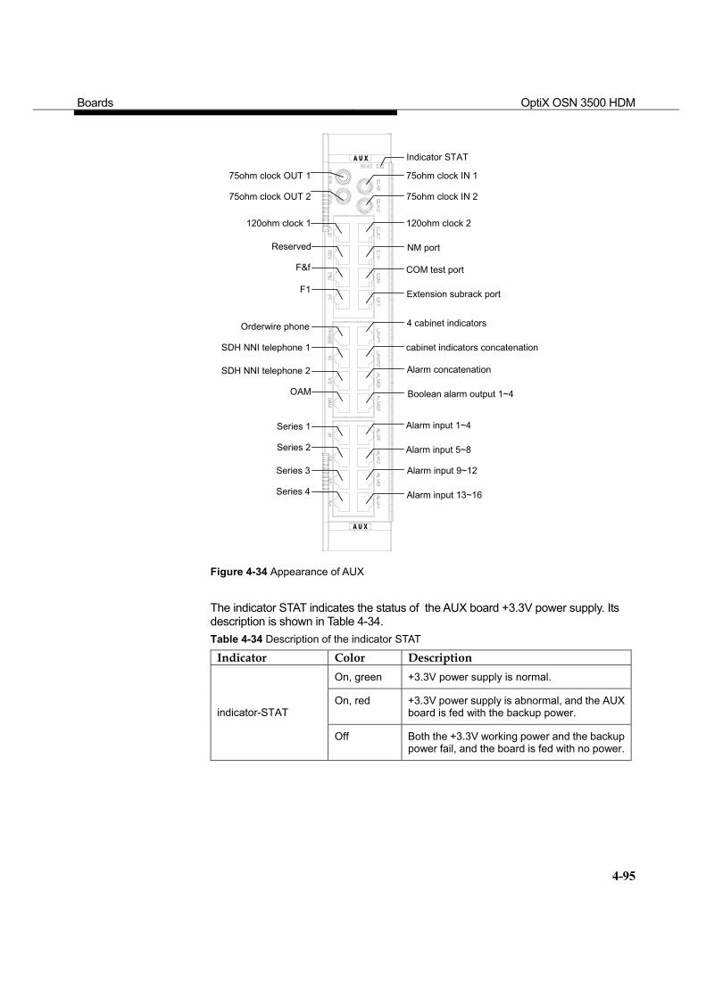
Boards OptiX OSN 3500 HDM
4-95
75ohm clock IN 1
75ohm clock IN 2
75ohm clock OUT 1
75ohm clock OUT 2
120ohm clock 2
NM port
COM test port
Extension subrack port
4 cabinet indicators
cabinet indicators concatenation
Alarm concatenation
Boolean alarm output 1~4
Alarm input 1~4
Alarm input 5~8
Alarm input 9~12
Alarm input 13~16
120ohm clock 1
Reserved
F&f
Orderwire phone
SDH NNI telephone 1
SDH NNI telephone 2
OAM
Series 1
Series 2
Series 3
Series 4
F1
Indicator STAT
Figure 4-34 Appearance of AUX The indicator STAT indicates the status of the AUX board +3.3V power supply. Its description is shown in Table 4-34. Table 4-34 Description of the indicator STAT
Indicator Color Description On, green +3.3V power supply is normal.
On, red +3.3V power supply is abnormal, and the AUX board is fed with the backup power. indicator-STAT
Off Both the +3.3V working power and the backup power fail, and the board is fed with no power.
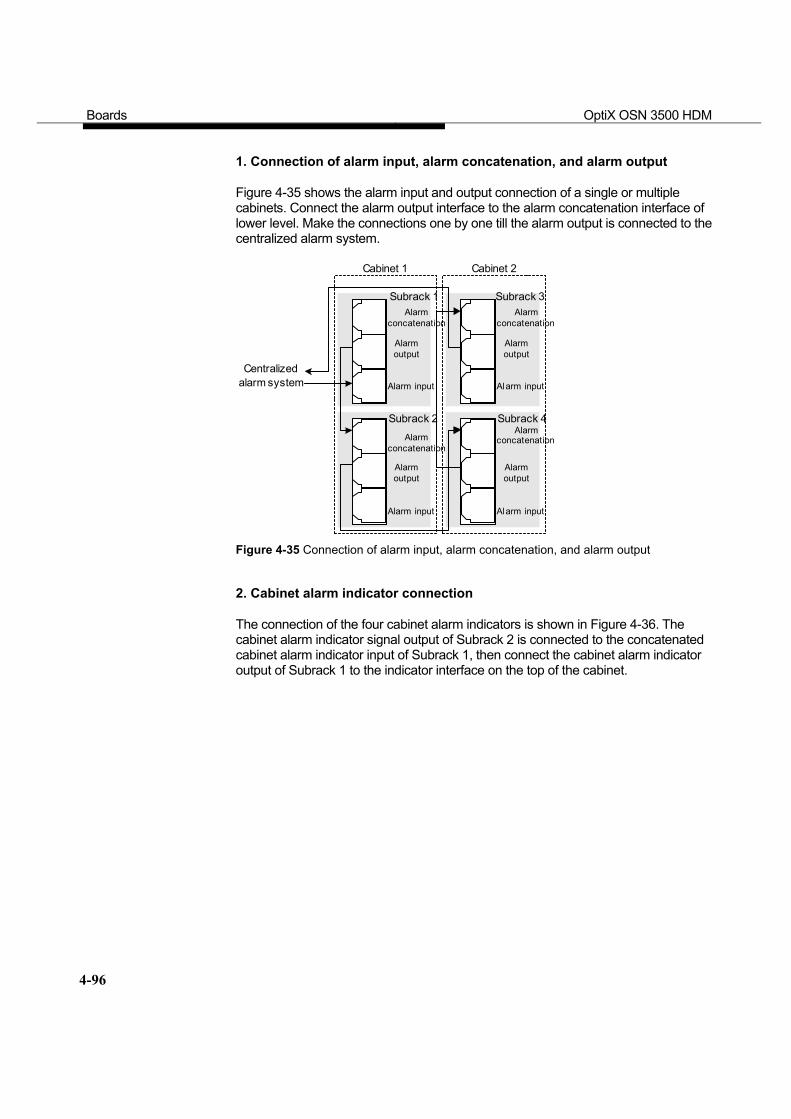
Boards OptiX OSN 3500 HDM
4-96
1. Connection of alarm input, alarm concatenation, and alarm output
Figure 4-35 shows the alarm input and output connection of a single or multiple cabinets. Connect the alarm output interface to the alarm concatenation interface of lower level. Make the connections one by one till the alarm output is connected to the centralized alarm system.
Cabinet 1 Cabinet 2
Subrack 1
Subrack 2
Subrack 3
Subrack 4
Alarmconcatenation
Alarmconcatenation
Alarmconcatenation
Alarmconcatenation
Alarmoutput
Alarmoutput
Alarmoutput
Alarmoutput
Alarm input
Alarm input
Alarm input
Alarm input
Centralizedalarm system
Figure 4-35 Connection of alarm input, alarm concatenation, and alarm output
2. Cabinet alarm indicator connection
The connection of the four cabinet alarm indicators is shown in Figure 4-36. The cabinet alarm indicator signal output of Subrack 2 is connected to the concatenated cabinet alarm indicator input of Subrack 1, then connect the cabinet alarm indicator output of Subrack 1 to the indicator interface on the top of the cabinet.
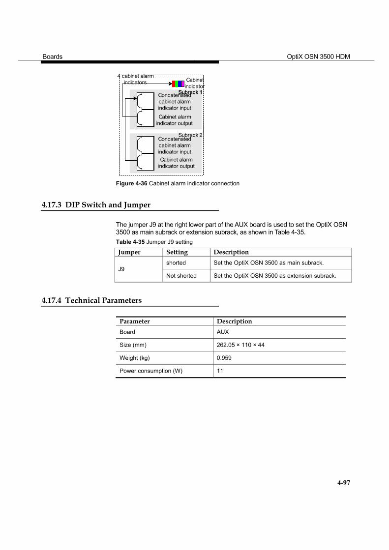
Boards OptiX OSN 3500 HDM
4-97
4 cabinet alarmindicators Cabinet
indicatorSubrack 1Subrack 1
Subrack 2
Concatenatedcabinet alarmindicator input
Concatenatedcabinet alarmindicator input
Cabinet alarmindicator output
Cabinet alarmindicator output
Figure 4-36 Cabinet alarm indicator connection
4.17.3 DIP Switch and Jumper
The jumper J9 at the right lower part of the AUX board is used to set the OptiX OSN 3500 as main subrack or extension subrack, as shown in Table 4-35. Table 4-35 Jumper J9 setting
Jumper Setting Description shorted Set the OptiX OSN 3500 as main subrack.
J9 Not shorted Set the OptiX OSN 3500 as extension subrack.
4.17.4 Technical Parameters
Parameter Description Board AUX
Size (mm) 262.05 × 110 × 44
Weight (kg) 0.959
Power consumption (W) 11
Boards OptiX OSN 3500 HDM
4-98
Parameter Description Environment parameter (optional) Long term operating condition
Temperature: 0°C ~ 40°C Humidity:20% ~ 90% Short term operating condition Temperature: -5°C ~ 50°C Humidity:20% ~ 90% Environment for Storage Temperature: -40°C ~ +70°C Humidity:10% ~ 100% Environment for Transportation Temperature: -40°C ~ +70°C Humidity:10% ~ 100%
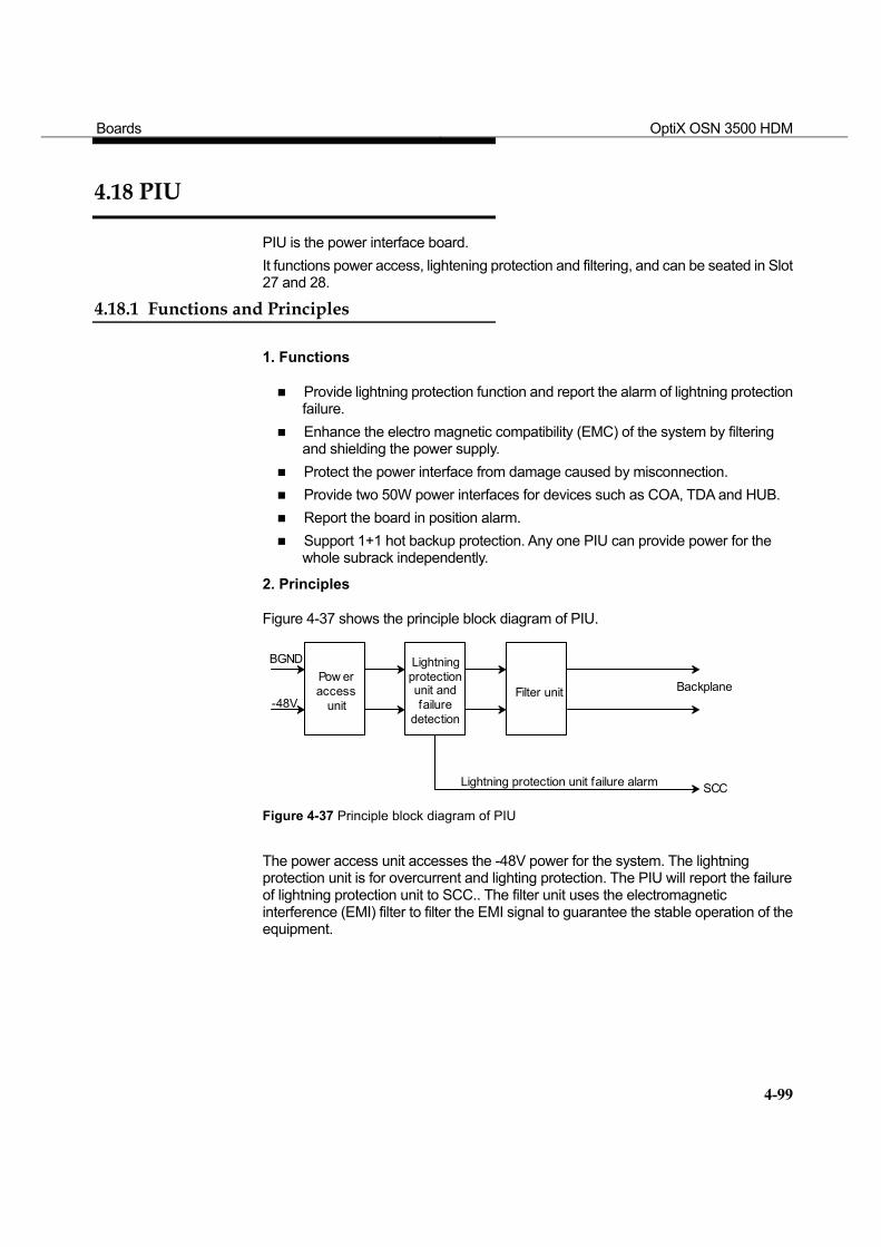
Boards OptiX OSN 3500 HDM
4-99
4.18 PIU
PIU is the power interface board. It functions power access, lightening protection and filtering, and can be seated in Slot 27 and 28.
4.18.1 Functions and Principles
1. Functions
Provide lightning protection function and report the alarm of lightning protection failure.
Enhance the electro magnetic compatibility (EMC) of the system by filtering and shielding the power supply.
Protect the power interface from damage caused by misconnection. Provide two 50W power interfaces for devices such as COA, TDA and HUB. Report the board in position alarm. Support 1+1 hot backup protection. Any one PIU can provide power for the
whole subrack independently.
2. Principles
Figure 4-37 shows the principle block diagram of PIU.
Backplane
BGND
SCC
Lightningprotectionunit andfailure
detection
Filter unit
Lightning protection unit failure alarm
-48V
Pow eraccess
unit
Figure 4-37 Principle block diagram of PIU The power access unit accesses the -48V power for the system. The lightning protection unit is for overcurrent and lighting protection. The PIU will report the failure of lightning protection unit to SCC.. The filter unit uses the electromagnetic interference (EMI) filter to filter the EMI signal to guarantee the stable operation of the equipment.
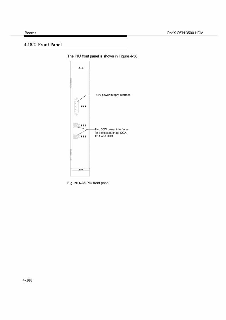
Boards OptiX OSN 3500 HDM
4-100
4.18.2 Front Panel
The PIU front panel is shown in Figure 4-38.
-48V power supply interface
Two 50W power interfacesfor devices such as COA,TDA and HUB
Figure 4-38 PIU front panel
Boards OptiX OSN 3500 HDM
4-101
4.18.3 Interface
See the figure Figure 4-38.
4.18.4 DIP Switch and Jumper
None.
4.18.5 Technical Parameters
Parameter Description Board PIU
Input voltage -38.4 ~ -72V
Protecion tube F7 250V-20A-0.00355Ω
Size (mm) 262.05 × 110 × 44
Weight (kg) 1.151
Power consumption (W) 8
Environment parameter (optional) Long term operating condition Temperature: 0°C ~ 40°C Humidity:20% ~ 90% Short term operating condition Temperature: -5°C ~ 50°C Humidity:20% ~ 90% Environment for Storage Temperature: -40°C ~ +70°C Humidity:10% ~ 100% Environment for Transportation Temperature: -40°C ~ +70°C Humidity:10% ~ 100%
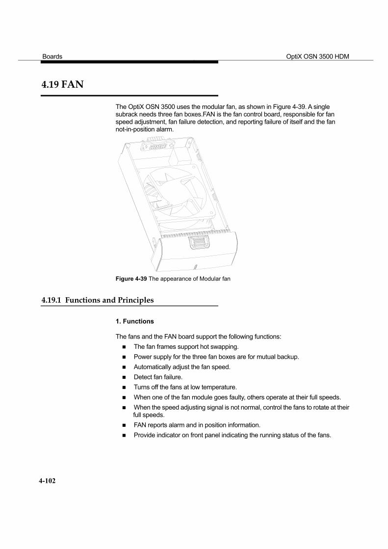
Boards OptiX OSN 3500 HDM
4-102
4.19 FAN
The OptiX OSN 3500 uses the modular fan, as shown in Figure 4-39. A single subrack needs three fan boxes.FAN is the fan control board, responsible for fan speed adjustment, fan failure detection, and reporting failure of itself and the fan not-in-position alarm.
Figure 4-39 The appearance of Modular fan
4.19.1 Functions and Principles
1. Functions
The fans and the FAN board support the following functions: The fan frames support hot swapping. Power supply for the three fan boxes are for mutual backup. Automatically adjust the fan speed. Detect fan failure. Turns off the fans at low temperature. When one of the fan module goes faulty, others operate at their full speeds. When the speed adjusting signal is not normal, control the fans to rotate at their
full speeds. FAN reports alarm and in position information. Provide indicator on front panel indicating the running status of the fans.
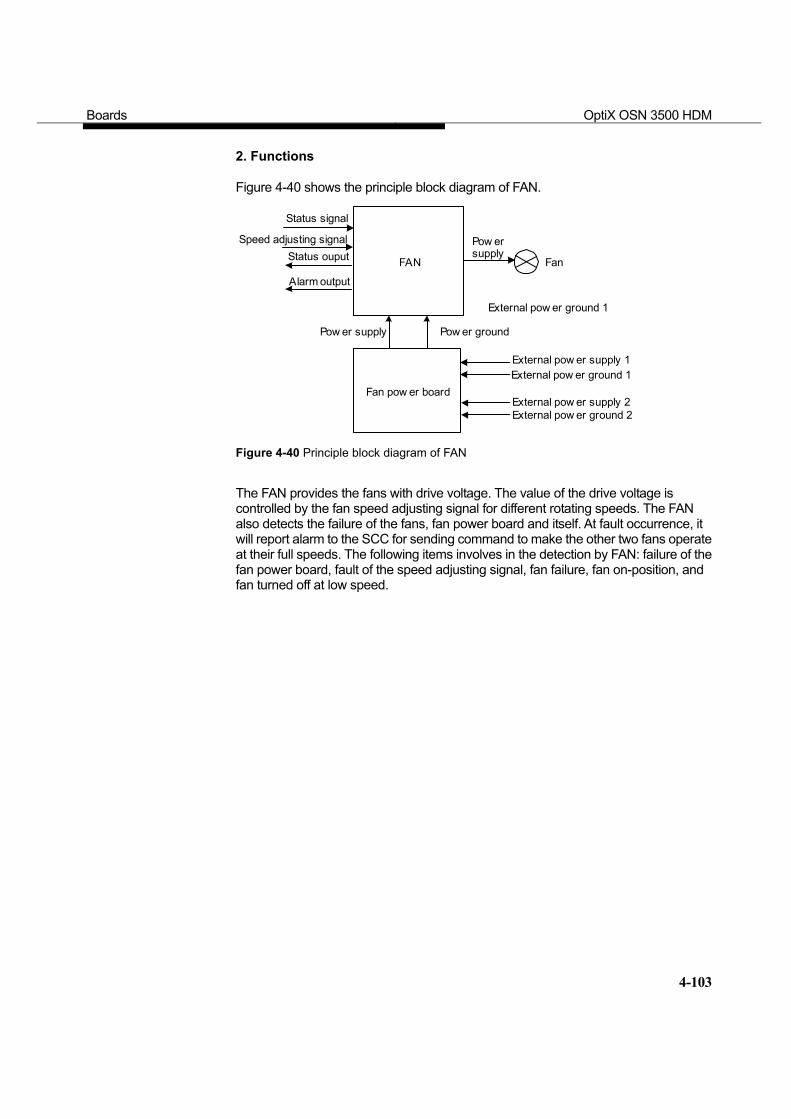
Boards OptiX OSN 3500 HDM
4-103
2. Functions
Figure 4-40 shows the principle block diagram of FAN.
Pow er supply
Status signal
Speed adjusting signalStatus ouput
Alarm output
FAN
Pow er ground
Pow ersupply
External pow er supply 1
Fan
External pow er supply 2
External pow er ground 1
External pow er ground 1
External pow er ground 2
Fan pow er board
Figure 4-40 Principle block diagram of FAN The FAN provides the fans with drive voltage. The value of the drive voltage is controlled by the fan speed adjusting signal for different rotating speeds. The FAN also detects the failure of the fans, fan power board and itself. At fault occurrence, it will report alarm to the SCC for sending command to make the other two fans operate at their full speeds. The following items involves in the detection by FAN: failure of the fan power board, fault of the speed adjusting signal, fan failure, fan on-position, and fan turned off at low speed.
Boards OptiX OSN 3500 HDM
4-104
4.19.2 Front Panel
The front panel of fan box provides a indicator that indicates the operation status of the fans and the FAN board. Its description is shown in Table 4-36. Table 4-36 Indicator description of the fan box
Indicator Color Description On, green The fan operates normally.
On, red The fan, fan power board or FAN is abnormal. Operation status indicator-STAT
On, yellow The fan is turned off due to low temperature.
4.19.3 Interface
None.
4.19.4 Technical Parameters
Size 50.8mm (H) x 120mm (W) x 120mm (D)
Weight (kg) 1.5
Power consumption (W) 30
Working voltage -48V ± 20% DC
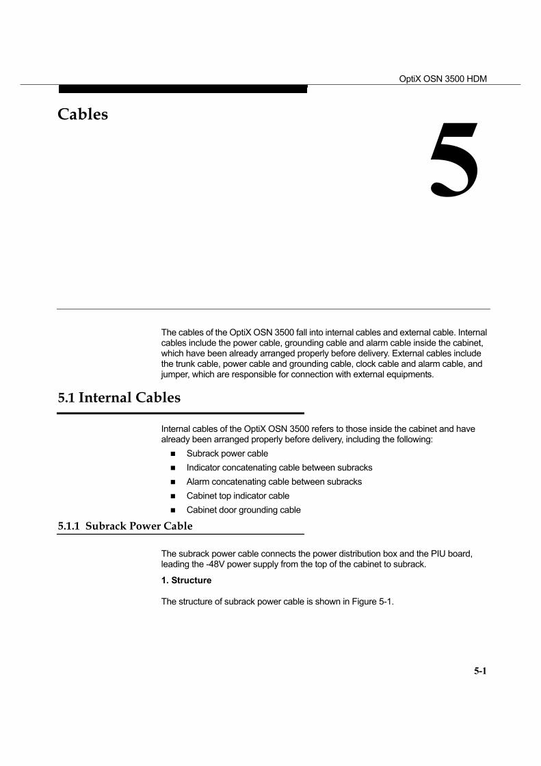
OptiX OSN 3500 HDM
5-1
5 Cables
The cables of the OptiX OSN 3500 fall into internal cables and external cable. Internal cables include the power cable, grounding cable and alarm cable inside the cabinet, which have been already arranged properly before delivery. External cables include the trunk cable, power cable and grounding cable, clock cable and alarm cable, and jumper, which are responsible for connection with external equipments.
5.1 Internal Cables
Internal cables of the OptiX OSN 3500 refers to those inside the cabinet and have already been arranged properly before delivery, including the following:
Subrack power cable Indicator concatenating cable between subracks Alarm concatenating cable between subracks Cabinet top indicator cable Cabinet door grounding cable
5.1.1 Subrack Power Cable
The subrack power cable connects the power distribution box and the PIU board, leading the -48V power supply from the top of the cabinet to subrack.
1. Structure
The structure of subrack power cable is shown in Figure 5-1.
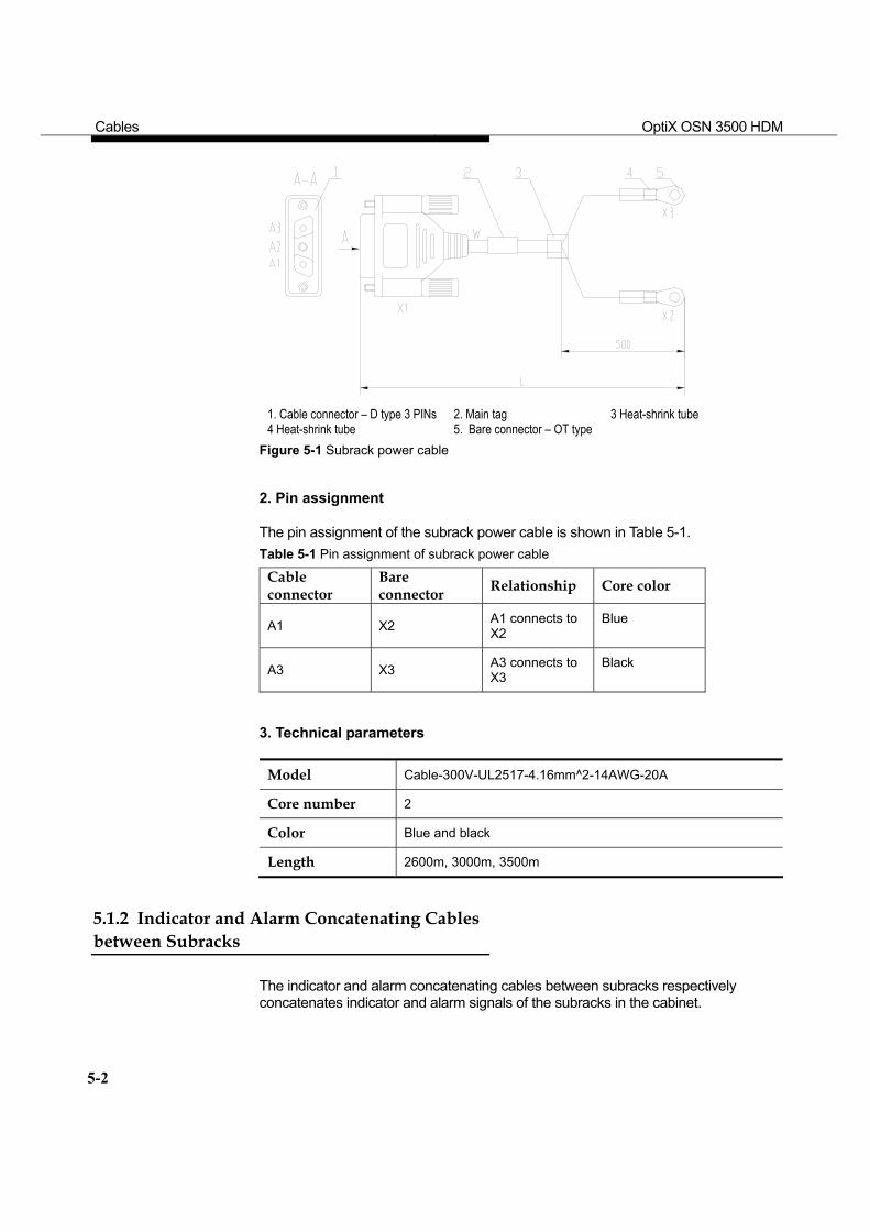
Cables OptiX OSN 3500 HDM
5-2
1. Cable connector – D type 3 PINs 2. Main tag 3 Heat-shrink tube 4 Heat-shrink tube 5. Bare connector – OT type
Figure 5-1 Subrack power cable
2. Pin assignment
The pin assignment of the subrack power cable is shown in Table 5-1. Table 5-1 Pin assignment of subrack power cable
Cable connector
Bare connector Relationship Core color
A1 X2 A1 connects to X2
Blue
A3 X3 A3 connects to X3
Black
3. Technical parameters
Model Cable-300V-UL2517-4.16mm^2-14AWG-20A
Core number 2
Color Blue and black
Length 2600m, 3000m, 3500m
5.1.2 Indicator and Alarm Concatenating Cables between Subracks
The indicator and alarm concatenating cables between subracks respectively concatenates indicator and alarm signals of the subracks in the cabinet.
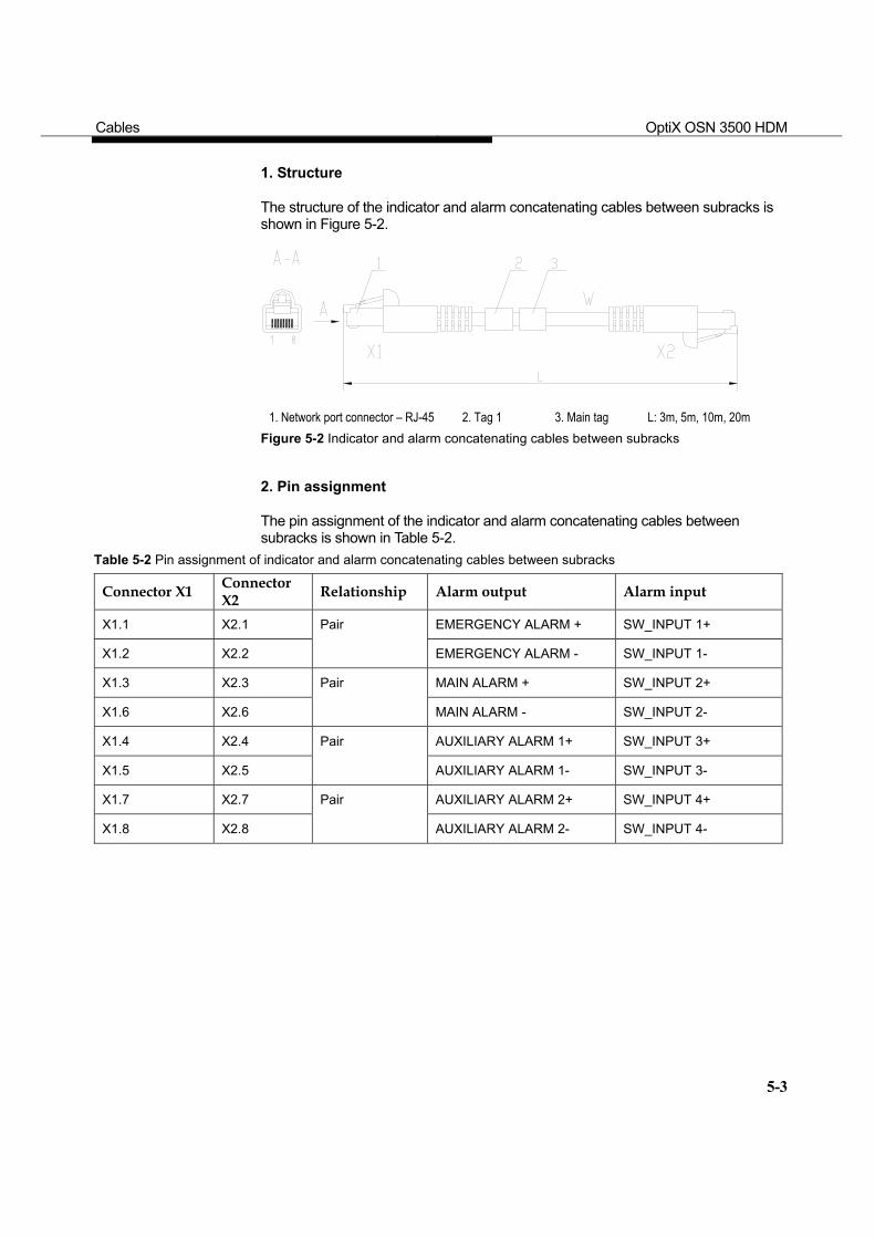
Cables OptiX OSN 3500 HDM
5-3
1. Structure
The structure of the indicator and alarm concatenating cables between subracks is shown in Figure 5-2.
1. Network port connector – RJ-45 2. Tag 1 3. Main tag L: 3m, 5m, 10m, 20m
Figure 5-2 Indicator and alarm concatenating cables between subracks
2. Pin assignment
The pin assignment of the indicator and alarm concatenating cables between subracks is shown in Table 5-2.
Table 5-2 Pin assignment of indicator and alarm concatenating cables between subracks
Connector X1 Connector X2 Relationship Alarm output Alarm input
X1.1 X2.1 EMERGENCY ALARM + SW_INPUT 1+
X1.2 X2.2
Pair
EMERGENCY ALARM - SW_INPUT 1-
X1.3 X2.3 MAIN ALARM + SW_INPUT 2+
X1.6 X2.6
Pair
MAIN ALARM - SW_INPUT 2-
X1.4 X2.4 AUXILIARY ALARM 1+ SW_INPUT 3+
X1.5 X2.5
Pair
AUXILIARY ALARM 1- SW_INPUT 3-
X1.7 X2.7 AUXILIARY ALARM 2+ SW_INPUT 4+
X1.8 X2.8
Pair
AUXILIARY ALARM 2- SW_INPUT 4-
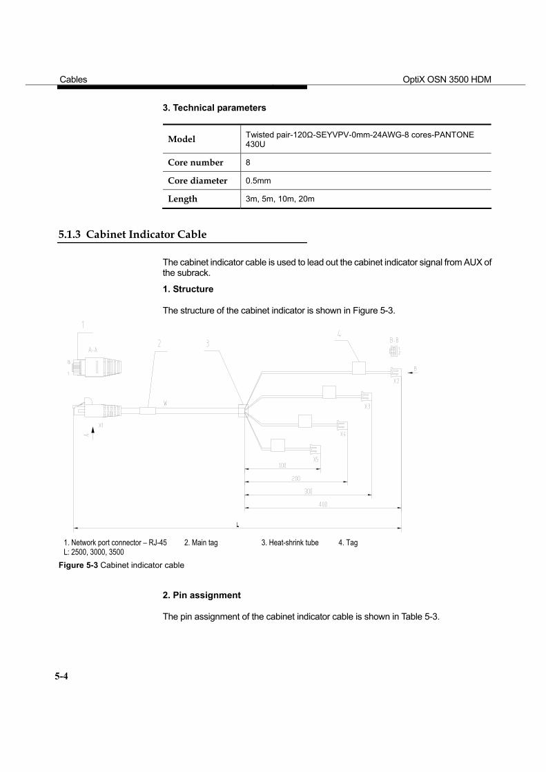
Cables OptiX OSN 3500 HDM
5-4
3. Technical parameters
Model Twisted pair-120Ω-SEYVPV-0mm-24AWG-8 cores-PANTONE 430U
Core number 8
Core diameter 0.5mm
Length 3m, 5m, 10m, 20m
5.1.3 Cabinet Indicator Cable
The cabinet indicator cable is used to lead out the cabinet indicator signal from AUX of the subrack.
1. Structure
The structure of the cabinet indicator is shown in Figure 5-3.
1. Network port connector – RJ-45 2. Main tag 3. Heat-shrink tube 4. Tag L: 2500, 3000, 3500
Figure 5-3 Cabinet indicator cable
2. Pin assignment
The pin assignment of the cabinet indicator cable is shown in Table 5-3.
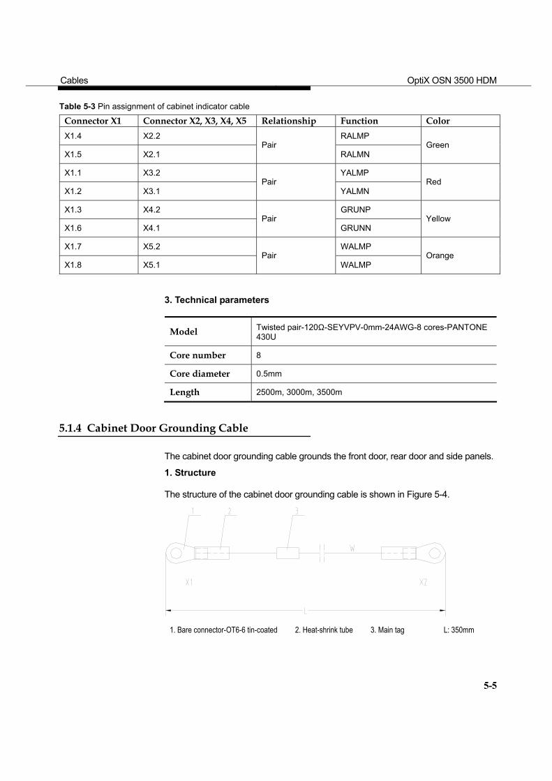
Cables OptiX OSN 3500 HDM
5-5
Table 5-3 Pin assignment of cabinet indicator cable
Connector X1 Connector X2, X3, X4, X5 Relationship Function Color X1.4 X2.2 RALMP
X1.5 X2.1 Pair
RALMN Green
X1.1 X3.2 YALMP
X1.2 X3.1 Pair
YALMN Red
X1.3 X4.2 GRUNP
X1.6 X4.1 Pair
GRUNN Yellow
X1.7 X5.2 WALMP
X1.8 X5.1 Pair
WALMP Orange
3. Technical parameters
Model Twisted pair-120Ω-SEYVPV-0mm-24AWG-8 cores-PANTONE 430U
Core number 8
Core diameter 0.5mm
Length 2500m, 3000m, 3500m
5.1.4 Cabinet Door Grounding Cable
The cabinet door grounding cable grounds the front door, rear door and side panels.
1. Structure
The structure of the cabinet door grounding cable is shown in Figure 5-4.
1. Bare connector-OT6-6 tin-coated 2. Heat-shrink tube 3. Main tag L: 350mm

Cables OptiX OSN 3500 HDM
5-6
Figure 5-4 Cabinet door grounding cable
2. Pin assignment
None
3. Technical parameters
Model Wire-600V-UL1015-10AWG-105-core twisted pair-yellow and green
Length 350mm
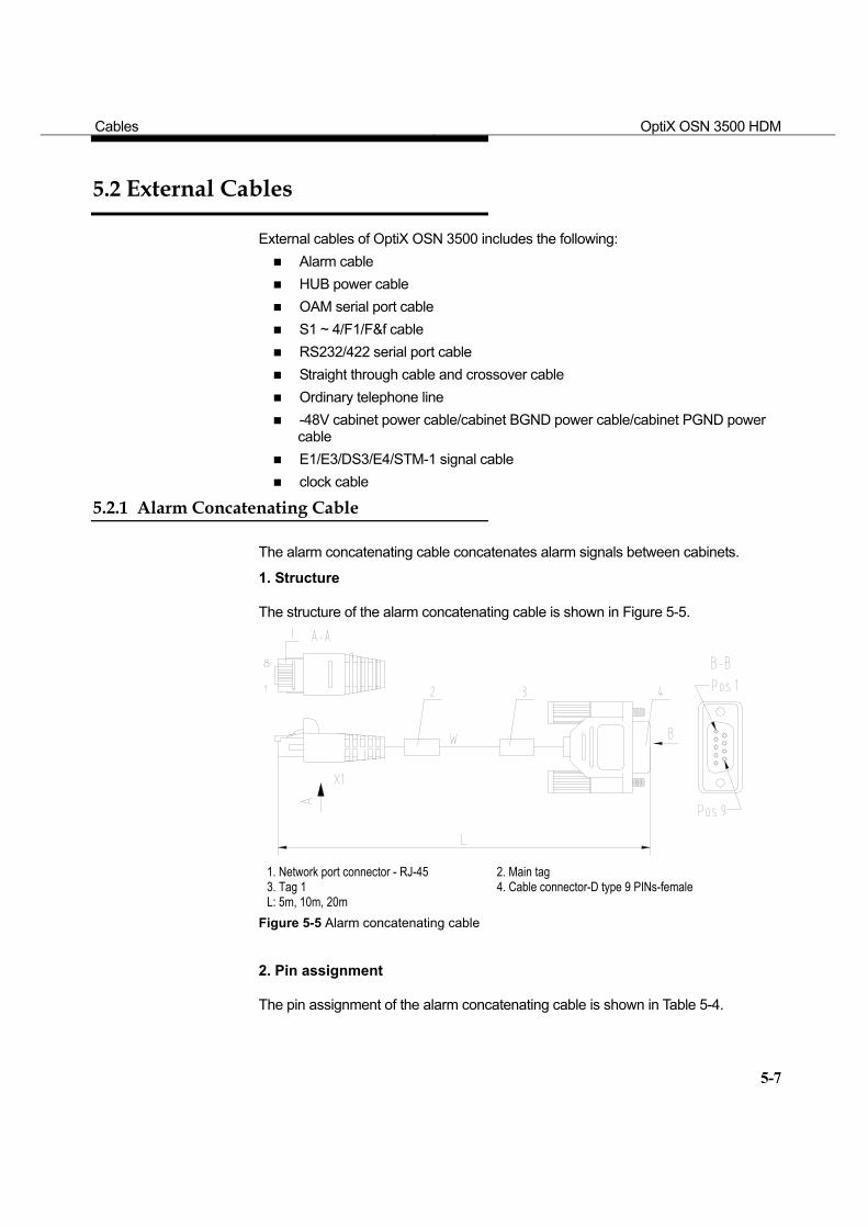
Cables OptiX OSN 3500 HDM
5-7
5.2 External Cables
External cables of OptiX OSN 3500 includes the following: Alarm cable HUB power cable OAM serial port cable S1 ~ 4/F1/F&f cable RS232/422 serial port cable Straight through cable and crossover cable Ordinary telephone line -48V cabinet power cable/cabinet BGND power cable/cabinet PGND power
cable E1/E3/DS3/E4/STM-1 signal cable clock cable
5.2.1 Alarm Concatenating Cable
The alarm concatenating cable concatenates alarm signals between cabinets.
1. Structure
The structure of the alarm concatenating cable is shown in Figure 5-5.
1. Network port connector - RJ-45 2. Main tag 3. Tag 1 4. Cable connector-D type 9 PINs-female L: 5m, 10m, 20m
Figure 5-5 Alarm concatenating cable
2. Pin assignment
The pin assignment of the alarm concatenating cable is shown in Table 5-4.
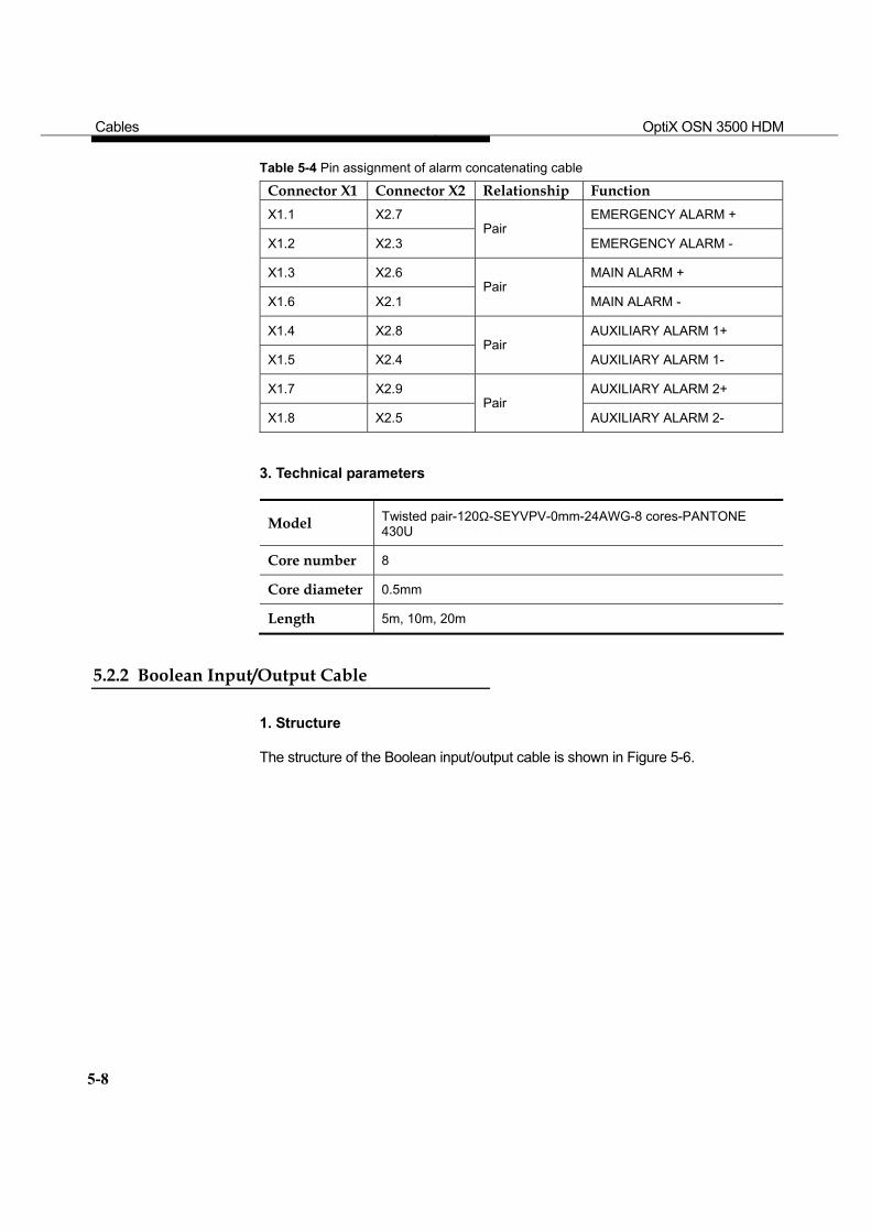
Cables OptiX OSN 3500 HDM
5-8
Table 5-4 Pin assignment of alarm concatenating cable
Connector X1 Connector X2 Relationship Function X1.1 X2.7 EMERGENCY ALARM +
X1.2 X2.3 Pair
EMERGENCY ALARM -
X1.3 X2.6 MAIN ALARM +
X1.6 X2.1 Pair
MAIN ALARM -
X1.4 X2.8 AUXILIARY ALARM 1+
X1.5 X2.4 Pair
AUXILIARY ALARM 1-
X1.7 X2.9 AUXILIARY ALARM 2+
X1.8 X2.5 Pair
AUXILIARY ALARM 2-
3. Technical parameters
Model Twisted pair-120Ω-SEYVPV-0mm-24AWG-8 cores-PANTONE 430U
Core number 8
Core diameter 0.5mm
Length 5m, 10m, 20m
5.2.2 Boolean Input/Output Cable
1. Structure
The structure of the Boolean input/output cable is shown in Figure 5-6.
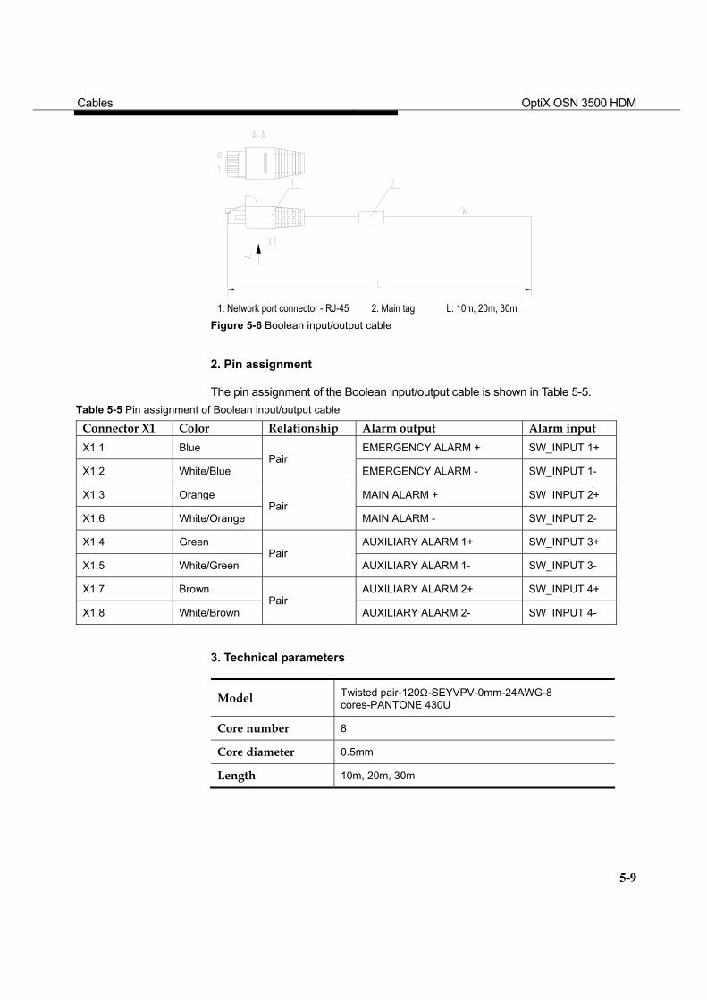
Cables OptiX OSN 3500 HDM
5-9
1. Network port connector - RJ-45 2. Main tag L: 10m, 20m, 30m
Figure 5-6 Boolean input/output cable
2. Pin assignment
The pin assignment of the Boolean input/output cable is shown in Table 5-5. Table 5-5 Pin assignment of Boolean input/output cable
Connector X1 Color Relationship Alarm output Alarm input X1.1 Blue EMERGENCY ALARM + SW_INPUT 1+
X1.2 White/Blue Pair
EMERGENCY ALARM - SW_INPUT 1-
X1.3 Orange MAIN ALARM + SW_INPUT 2+
X1.6 White/Orange Pair
MAIN ALARM - SW_INPUT 2-
X1.4 Green AUXILIARY ALARM 1+ SW_INPUT 3+
X1.5 White/Green Pair
AUXILIARY ALARM 1- SW_INPUT 3-
X1.7 Brown AUXILIARY ALARM 2+ SW_INPUT 4+
X1.8 White/Brown Pair
AUXILIARY ALARM 2- SW_INPUT 4-
3. Technical parameters
Model Twisted pair-120Ω-SEYVPV-0mm-24AWG-8 cores-PANTONE 430U
Core number 8
Core diameter 0.5mm
Length 10m, 20m, 30m
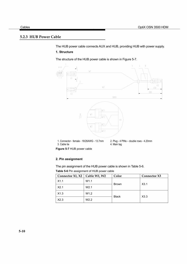
Cables OptiX OSN 3500 HDM
5-10
5.2.3 HUB Power Cable
The HUB power cable connects AUX and HUB, providing HUB with power supply.
1. Structure
The structure of the HUB power cable is shown in Figure 5-7.
1. Connector - female - 18/26AWG - 13.7mm 2. Plug - 4 PINs – double rows - 4.20mm 3. Cable tie 4. Main tag
Figure 5-7 HUB power cable
2. Pin assignment
The pin assignment of the HUB power cable is shown in Table 5-6. Table 5-6 Pin assignment of HUB power cable
Connector X1, X2 Cable W1, W2 Color Connector X3 X1.1 W1.1
X2.1 W2.1 Brown X3.1
X1.3 W1.2
X2.3 W2.2 Black X3.3
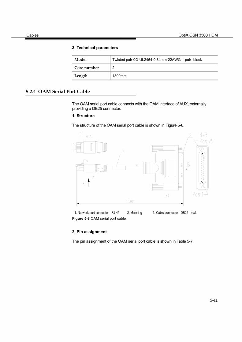
Cables OptiX OSN 3500 HDM
5-11
3. Technical parameters
Model Twisted pair-0Ω-UL2464-0.64mm-22AWG-1 pair -black
Core number 2
Length 1800mm
5.2.4 OAM Serial Port Cable
The OAM serial port cable connects with the OAM interface of AUX, externally providing a DB25 connector.
1. Structure
The structure of the OAM serial port cable is shown in Figure 5-8.
1. Network port connector - RJ-45 2. Main tag 3. Cable connector - DB25 - male
Figure 5-8 OAM serial port cable
2. Pin assignment
The pin assignment of the OAM serial port cable is shown in Table 5-7.
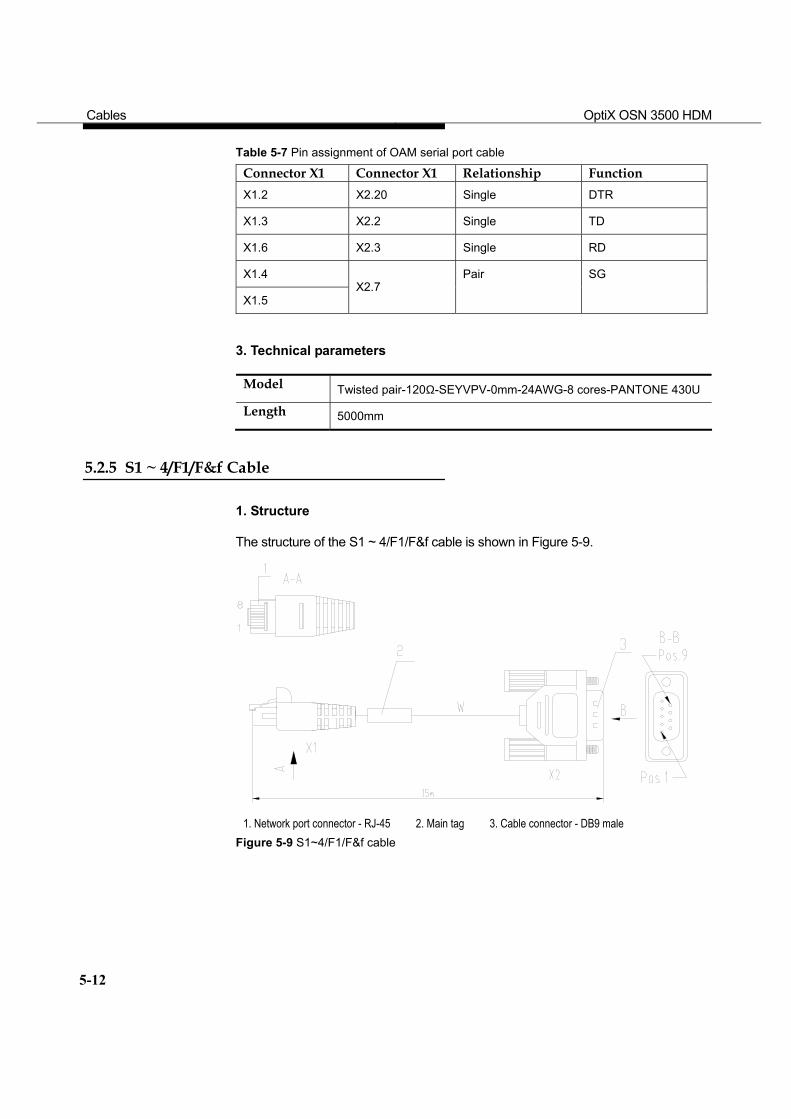
Cables OptiX OSN 3500 HDM
5-12
Table 5-7 Pin assignment of OAM serial port cable
Connector X1 Connector X1 Relationship Function X1.2 X2.20 Single DTR
X1.3 X2.2 Single TD
X1.6 X2.3 Single RD
X1.4
X1.5 X2.7
Pair SG
3. Technical parameters
Model Twisted pair-120Ω-SEYVPV-0mm-24AWG-8 cores-PANTONE 430U
Length 5000mm
5.2.5 S1 ~ 4/F1/F&f Cable
1. Structure
The structure of the S1 ~ 4/F1/F&f cable is shown in Figure 5-9.
1. Network port connector - RJ-45 2. Main tag 3. Cable connector - DB9 male
Figure 5-9 S1~4/F1/F&f cable
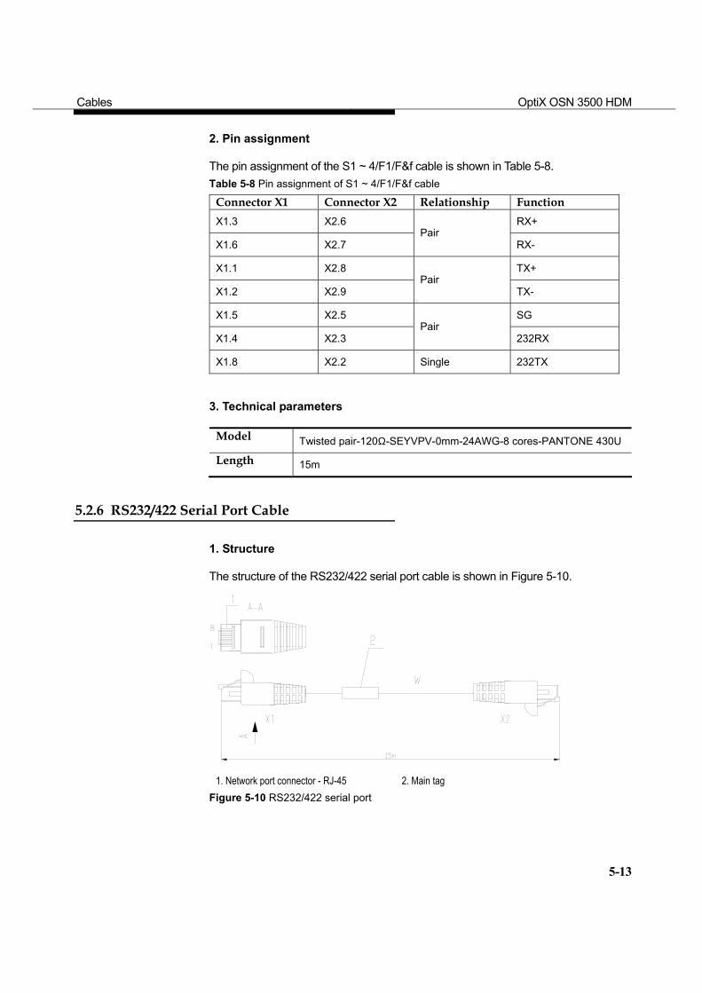
Cables OptiX OSN 3500 HDM
5-13
2. Pin assignment
The pin assignment of the S1 ~ 4/F1/F&f cable is shown in Table 5-8. Table 5-8 Pin assignment of S1 ~ 4/F1/F&f cable
Connector X1 Connector X2 Relationship Function X1.3 X2.6 RX+
X1.6 X2.7 Pair
RX-
X1.1 X2.8 TX+
X1.2 X2.9 Pair
TX-
X1.5 X2.5 SG
X1.4 X2.3 Pair
232RX
X1.8 X2.2 Single 232TX
3. Technical parameters
Model Twisted pair-120Ω-SEYVPV-0mm-24AWG-8 cores-PANTONE 430U
Length 15m
5.2.6 RS232/422 Serial Port Cable
1. Structure
The structure of the RS232/422 serial port cable is shown in Figure 5-10.
1. Network port connector - RJ-45 2. Main tag
Figure 5-10 RS232/422 serial port
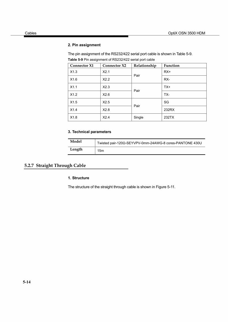
Cables OptiX OSN 3500 HDM
5-14
2. Pin assignment
The pin assignment of the RS232/422 serial port cable is shown in Table 5-9. Table 5-9 Pin assignment of RS232/422 serial port cable
Connector X1 Connector X2 Relationship Function X1.3 X2.1 RX+
X1.6 X2.2 Pair
RX-
X1.1 X2.3 TX+
X1.2 X2.6 Pair
TX-
X1.5 X2.5 SG
X1.4 X2.8 Pair
232RX
X1.8 X2.4 Single 232TX
3. Technical parameters
Model Twisted pair-120Ω-SEYVPV-0mm-24AWG-8 cores-PANTONE 430U
Length 15m
5.2.7 Straight Through Cable
1. Structure
The structure of the straight through cable is shown in Figure 5-11.
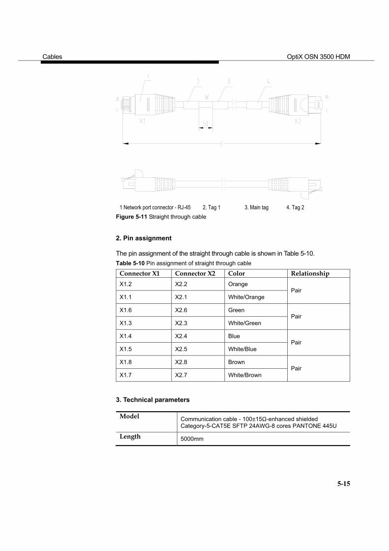
Cables OptiX OSN 3500 HDM
5-15
1 Network port connector - RJ-45 2. Tag 1 3. Main tag 4. Tag 2
Figure 5-11 Straight through cable
2. Pin assignment
The pin assignment of the straight through cable is shown in Table 5-10. Table 5-10 Pin assignment of straight through cable
Connector X1 Connector X2 Color Relationship X1.2 X2.2 Orange
X1.1 X2.1 White/Orange Pair
X1.6 X2.6 Green
X1.3 X2.3 White/Green Pair
X1.4 X2.4 Blue
X1.5 X2.5 White/Blue Pair
X1.8 X2.8 Brown
X1.7 X2.7 White/Brown Pair
3. Technical parameters
Model Communication cable - 100±15Ω-enhanced shielded Category-5-CAT5E SFTP 24AWG-8 cores PANTONE 445U
Length 5000mm
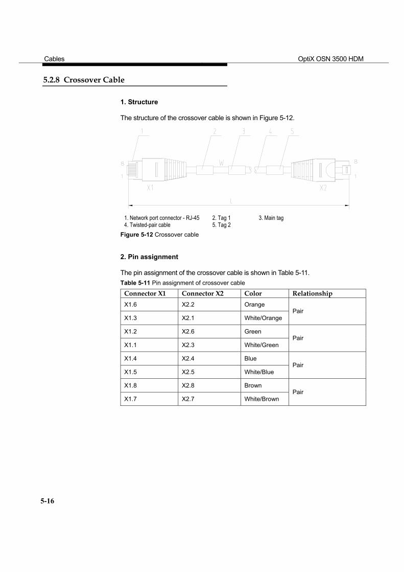
Cables OptiX OSN 3500 HDM
5-16
5.2.8 Crossover Cable
1. Structure
The structure of the crossover cable is shown in Figure 5-12.
1. Network port connector - RJ-45 2. Tag 1 3. Main tag 4. Twisted-pair cable 5. Tag 2
Figure 5-12 Crossover cable
2. Pin assignment
The pin assignment of the crossover cable is shown in Table 5-11. Table 5-11 Pin assignment of crossover cable
Connector X1 Connector X2 Color Relationship X1.6 X2.2 Orange
X1.3 X2.1 White/Orange Pair
X1.2 X2.6 Green
X1.1 X2.3 White/Green Pair
X1.4 X2.4 Blue
X1.5 X2.5 White/Blue Pair
X1.8 X2.8 Brown
X1.7 X2.7 White/Brown Pair
Cables OptiX OSN 3500 HDM
5-17
3. Technical parameters
Model Communication cable - 100±15Ω-enhanced shielded Category-5-CAT5E SFTP 24AWG-8 cores PANTONE 646U
Length 5m, 30m
5.2.9 75° Angle Straight Through Cable
1. Structure
The structure of the 75° angle straight through cable is shown in Figure 5-13.
1. Network port connector - RJ-45 2. Tag 1 3. Main tag 4. Tag 2
Figure 5-13 75° angle straight through cable
2. Pin assignment
The pin assignment of the 75° angle straight through cable is shown in Table 5-12. Table 5-12 Pin assignment of 75° angle straight through cable
Connector X1 Connector X2 Color Relationship X1.2 X2.2 Orange
X1.1 X2.1 White/Orange Pair
X1.6 X2.6 Green
X1.3 X2.3 White/Green Pair
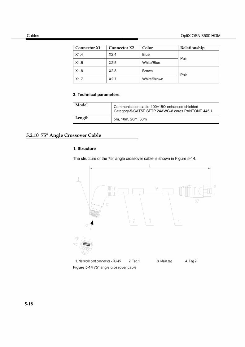
Cables OptiX OSN 3500 HDM
5-18
Connector X1 Connector X2 Color Relationship X1.4 X2.4 Blue
X1.5 X2.5 White/Blue Pair
X1.8 X2.8 Brown
X1.7 X2.7 White/Brown Pair
3. Technical parameters
Model Communication cable-100±15Ω-enhanced shielded Category-5-CAT5E SFTP 24AWG-8 cores PANTONE 445U
Length 5m, 10m, 20m, 30m
5.2.10 75° Angle Crossover Cable
1. Structure
The structure of the 75° angle crossover cable is shown in Figure 5-14.
1. Network port connector - RJ-45 2. Tag 1 3. Main tag 4. Tag 2
Figure 5-14 75° angle crossover cable
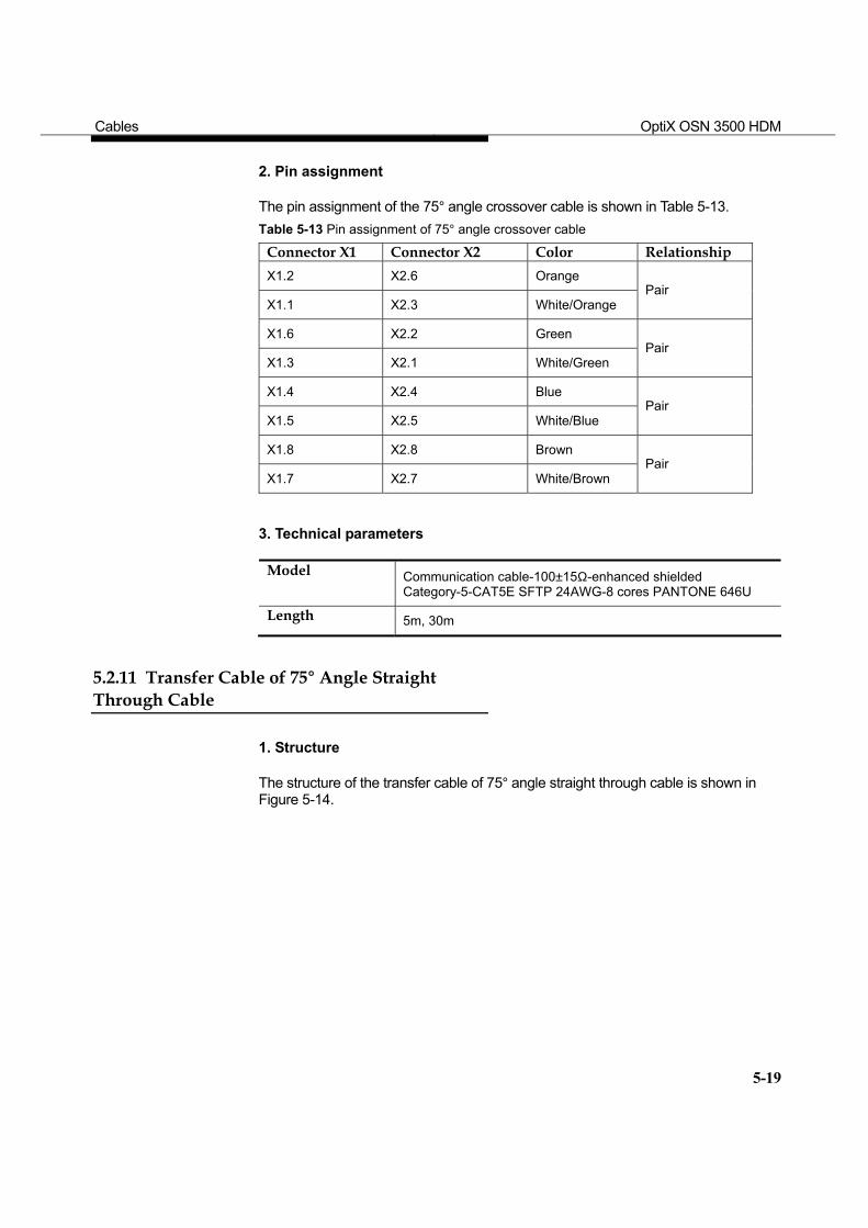
Cables OptiX OSN 3500 HDM
5-19
2. Pin assignment
The pin assignment of the 75° angle crossover cable is shown in Table 5-13. Table 5-13 Pin assignment of 75° angle crossover cable
Connector X1 Connector X2 Color Relationship X1.2 X2.6 Orange
X1.1 X2.3 White/Orange Pair
X1.6 X2.2 Green
X1.3 X2.1 White/Green Pair
X1.4 X2.4 Blue
X1.5 X2.5 White/Blue Pair
X1.8 X2.8 Brown
X1.7 X2.7 White/Brown Pair
3. Technical parameters
Model Communication cable-100±15Ω-enhanced shielded Category-5-CAT5E SFTP 24AWG-8 cores PANTONE 646U
Length 5m, 30m
5.2.11 Transfer Cable of 75° Angle Straight Through Cable
1. Structure
The structure of the transfer cable of 75° angle straight through cable is shown in Figure 5-14.
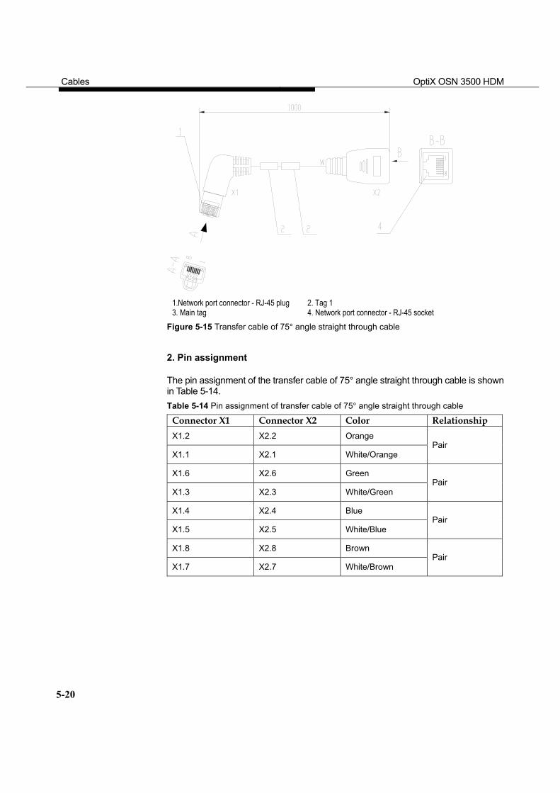
Cables OptiX OSN 3500 HDM
5-20
1.Network port connector - RJ-45 plug 2. Tag 1 3. Main tag 4. Network port connector - RJ-45 socket
Figure 5-15 Transfer cable of 75° angle straight through cable
2. Pin assignment
The pin assignment of the transfer cable of 75° angle straight through cable is shown in Table 5-14. Table 5-14 Pin assignment of transfer cable of 75° angle straight through cable
Connector X1 Connector X2 Color Relationship X1.2 X2.2 Orange
X1.1 X2.1 White/Orange Pair
X1.6 X2.6 Green
X1.3 X2.3 White/Green Pair
X1.4 X2.4 Blue
X1.5 X2.5 White/Blue Pair
X1.8 X2.8 Brown
X1.7 X2.7 White/Brown Pair
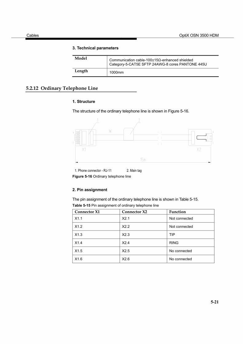
Cables OptiX OSN 3500 HDM
5-21
3. Technical parameters
Model Communication cable-100±15Ω-enhanced shielded Category-5-CAT5E SFTP 24AWG-8 cores PANTONE 445U
Length 1000mm
5.2.12 Ordinary Telephone Line
1. Structure
The structure of the ordinary telephone line is shown in Figure 5-16.
1. Phone connector - RJ-11 2. Main tag
Figure 5-16 Ordinary telephone line
2. Pin assignment
The pin assignment of the ordinary telephone line is shown in Table 5-15. Table 5-15 Pin assignment of ordinary telephone line
Connector X1 Connector X2 Function X1.1 X2.1 Not connected
X1.2 X2.2 Not connected
X1.3 X2.3 TIP
X1.4 X2.4 RING
X1.5 X2.5 No connected
X1.6 X2.6 No connected
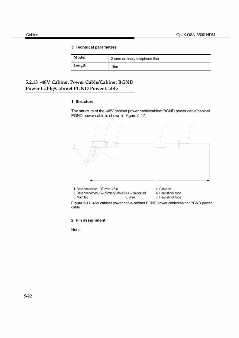
Cables OptiX OSN 3500 HDM
5-22
3. Technical parameters
Model 2-core ordinary telephone line
Length 15m
5.2.13 -48V Cabinet Power Cable/Cabinet BGND Power Cable/Cabinet PGND Power Cable
1. Structure
The structure of the -48V cabinet power cable/cabinet BGND power cable/cabinet PGND power cable is shown in Figure 5-17.
1. Bare connector - OT type -25-8 2. Cable tie 3. Bare connector-JG2-25mm^2-M6-150.A – tin-coated 4. Heat-shrink tube 5. Main tag 6. Wire 7. Heat-shrink tube
Figure 5-17 -48V cabinet power cable/cabinet BGND power cable/cabinet PGND power cable
2. Pin assignment
None
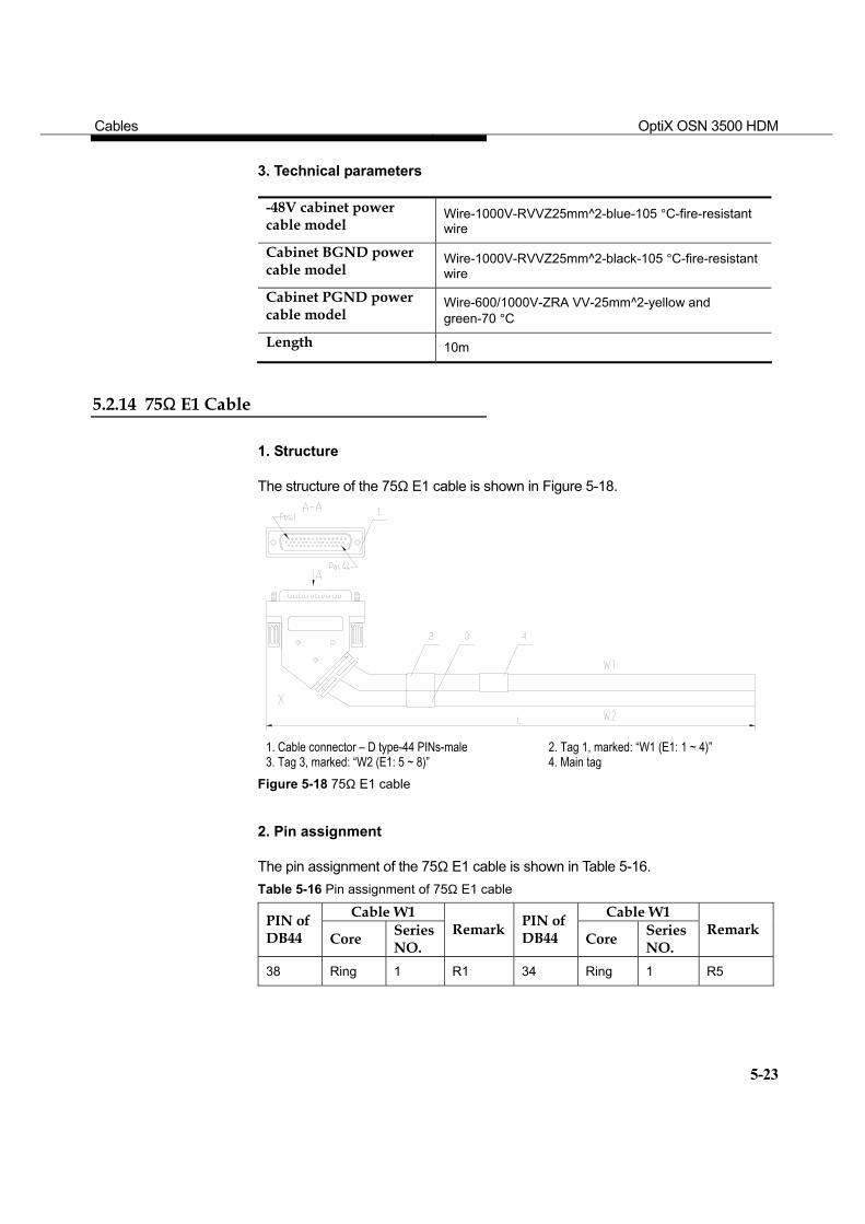
Cables OptiX OSN 3500 HDM
5-23
3. Technical parameters
-48V cabinet power cable model
Wire-1000V-RVVZ25mm^2-blue-105 °C-fire-resistant wire
Cabinet BGND power cable model
Wire-1000V-RVVZ25mm^2-black-105 °C-fire-resistant wire
Cabinet PGND power cable model
Wire-600/1000V-ZRA VV-25mm^2-yellow and green-70 °C
Length 10m
5.2.14 75Ω E1 Cable
1. Structure
The structure of the 75Ω E1 cable is shown in Figure 5-18.
1. Cable connector – D type-44 PINs-male 2. Tag 1, marked: “W1 (E1: 1 ~ 4)” 3. Tag 3, marked: “W2 (E1: 5 ~ 8)” 4. Main tag
Figure 5-18 75Ω E1 cable
2. Pin assignment
The pin assignment of the 75Ω E1 cable is shown in Table 5-16. Table 5-16 Pin assignment of 75Ω E1 cable
Cable W1 Cable W1 PIN of DB44 Core Series
NO. Remark PIN of
DB44 Core Series NO.
Remark
38 Ring 1 R1 34 Ring 1 R5
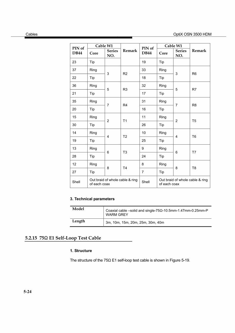
Cables OptiX OSN 3500 HDM
5-24
Cable W1 Cable W1 PIN of DB44 Core Series
NO. Remark PIN of
DB44 Core Series NO.
Remark
23 Tip 19 Tip
37 Ring 33 Ring
22 Tip 3 R2
18 Tip 3 R6
36 Ring 32 Ring
21 Tip 5 R3
17 Tip 5 R7
35 Ring 31 Ring
20 Tip 7 R4
16 Tip 7 R8
15 Ring 11 Ring
30 Tip 2 T1
26 Tip 2 T5
14 Ring 10 Ring
19 Tip 4 T2
25 Tip 4 T6
13 Ring 9 Ring
28 Tip 6 T3
24 Tip 6 T7
12 Ring 8 Ring
27 Tip 8 T4
7 Tip 8 T8
Shell Out braid of whole cable & ring of each coax Shell Out braid of whole cable & ring
of each coax
3. Technical parameters
Model Coaxial cable –solid and single-75Ω-10.5mm-1.47mm-0.25mm-P WARM GREY
Length 3m, 10m, 15m, 20m, 25m, 30m, 40m
5.2.15 75Ω E1 Self-Loop Test Cable
1. Structure
The structure of the 75Ω E1 self-loop test cable is shown in Figure 5-19.
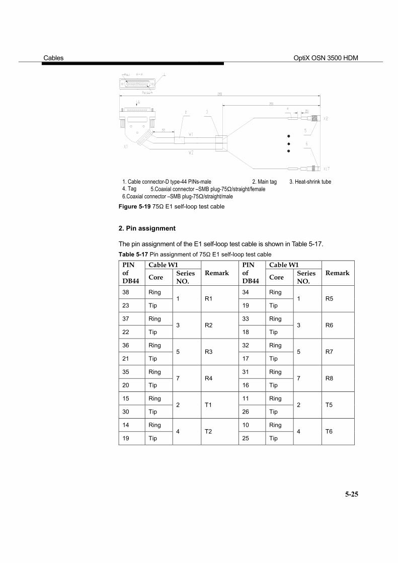
Cables OptiX OSN 3500 HDM
5-25
1. Cable connector-D type-44 PINs-male 2. Main tag 3. Heat-shrink tube 4. Tag 5.Coaxial connector –SMB plug-75Ω/straight/female 6.Coaxial connector –SMB plug-75Ω/straight/male
Figure 5-19 75Ω E1 self-loop test cable
2. Pin assignment
The pin assignment of the E1 self-loop test cable is shown in Table 5-17. Table 5-17 Pin assignment of 75Ω E1 self-loop test cable
Cable W1 Cable W1 PIN of DB44 Core Series
NO. Remark
PIN of DB44 Core Series
NO. Remark
38 Ring 34 Ring
23 Tip 1 R1
19 Tip 1 R5
37 Ring 33 Ring
22 Tip 3 R2
18 Tip 3 R6
36 Ring 32 Ring
21 Tip 5 R3
17 Tip 5 R7
35 Ring 31 Ring
20 Tip 7 R4
16 Tip 7 R8
15 Ring 11 Ring
30 Tip 2 T1
26 Tip 2 T5
14 Ring 10 Ring
19 Tip 4 T2
25 Tip 4 T6
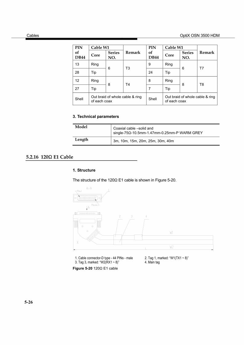
Cables OptiX OSN 3500 HDM
5-26
Cable W1 Cable W1 PIN of DB44 Core Series
NO. Remark
PIN of DB44 Core Series
NO. Remark
13 Ring 9 Ring
28 Tip 6 T3
24 Tip 6 T7
12 Ring 8 Ring
27 Tip 8 T4
7 Tip 8 T8
Shell Out braid of whole cable & ring of each coax Shell Out braid of whole cable & ring
of each coax
3. Technical parameters
Model Coaxial cable –solid and single-75Ω-10.5mm-1.47mm-0.25mm-P WARM GREY
Length 3m, 10m, 15m, 20m, 25m, 30m, 40m
5.2.16 120Ω E1 Cable
1. Structure
The structure of the 120Ω E1 cable is shown in Figure 5-20.
1. Cable connector-D type - 44 PINs - male 2. Tag 1, marked: “W1(TX1 ~ 8)” 3. Tag 3, marked: “W2(RX1 ~ 8)” 4. Main tag
Figure 5-20 120Ω E1 cable
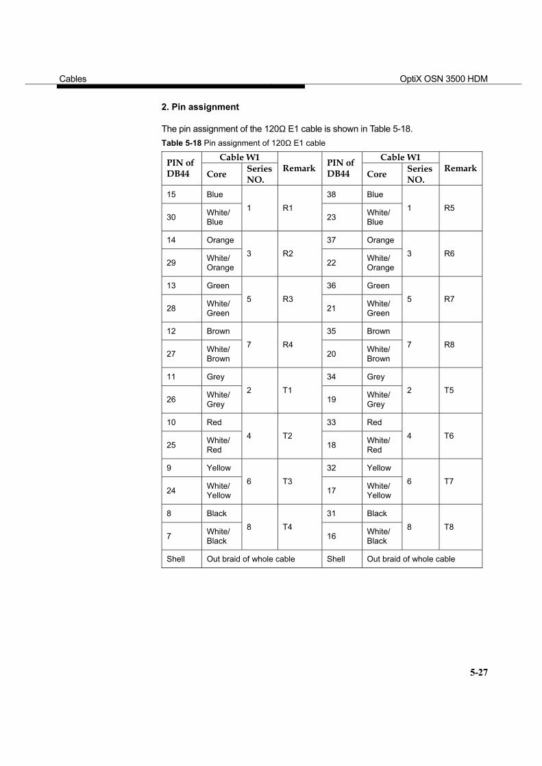
Cables OptiX OSN 3500 HDM
5-27
2. Pin assignment
The pin assignment of the 120Ω E1 cable is shown in Table 5-18. Table 5-18 Pin assignment of 120Ω E1 cable
Cable W1 Cable W1 PIN of DB44 Core Series
NO. Remark PIN of
DB44 Core Series NO.
Remark
15 Blue 38 Blue
30 White/ Blue
1 R1 23 White/
Blue 1 R5
14 Orange 37 Orange
29 White/ Orange
3 R2 22 White/
Orange 3 R6
13 Green 36 Green
28 White/ Green
5 R3 21 White/
Green
5 R7
12 Brown 35 Brown
27 White/ Brown
7 R4 20 White/
Brown
7 R8
11 Grey 34 Grey
26 White/ Grey
2 T1 19 White/
Grey 2 T5
10 Red 33 Red
25 White/ Red
4 T2 18 White/
Red 4 T6
9 Yellow 32 Yellow
24 White/ Yellow
6 T3 17 White/
Yellow 6 T7
8 Black 31 Black
7 White/ Black
8 T4 16 White/
Black 8 T8
Shell Out braid of whole cable Shell Out braid of whole cable
Cables OptiX OSN 3500 HDM
5-28
3. Technical parameters
Model Communication cable - 120Ω - SEYPVPV - 24AWG - 16 cores - PANTONE 430U
Length 10m, 15m, 20m, 30m, 40m
5.2.17 E3/DS3 Cable
1. Structure
The structure of E3/DS3 cable is shown in Figure 5-21.
1. Coaxial connector -SMB-75Ω-straight/plug- female -RG59 2. Main tag 3. Coaxial cable
Figure 5-21 E3/DS3 cable
2. Pin assignment
None
3. Technical parameters
Model Coaxial cable -RG59/U-75Ω-insulation outer diameter: 3.71mm-single/0.643 - bare copper wire
Length 30m
5.2.18 STM-1 Cable
1. Structure
The structure of the STM-1 cable is shown in Figure 5-22.
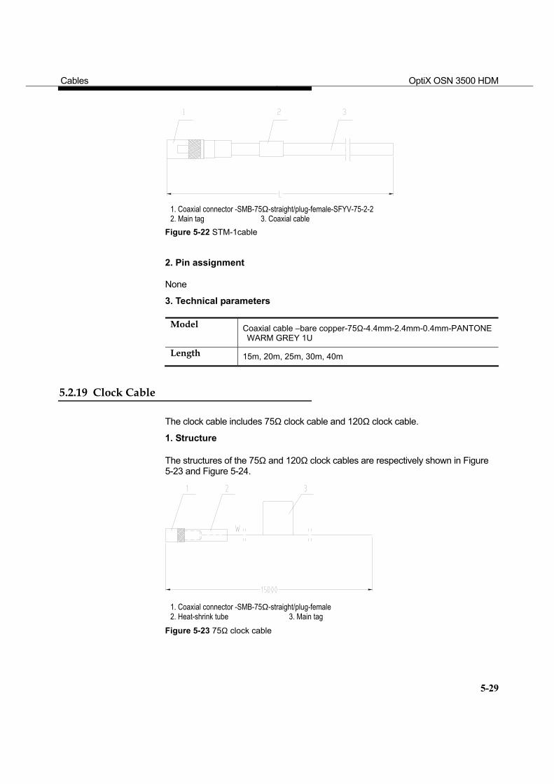
Cables OptiX OSN 3500 HDM
5-29
1. Coaxial connector -SMB-75Ω-straight/plug-female-SFYV-75-2-2 2. Main tag 3. Coaxial cable
Figure 5-22 STM-1cable
2. Pin assignment
None
3. Technical parameters
Model Coaxial cable –bare copper-75Ω-4.4mm-2.4mm-0.4mm-PANTONE WARM GREY 1U
Length 15m, 20m, 25m, 30m, 40m
5.2.19 Clock Cable
The clock cable includes 75Ω clock cable and 120Ω clock cable.
1. Structure
The structures of the 75Ω and 120Ω clock cables are respectively shown in Figure 5-23 and Figure 5-24.
1. Coaxial connector -SMB-75Ω-straight/plug-female 2. Heat-shrink tube 3. Main tag
Figure 5-23 75Ω clock cable
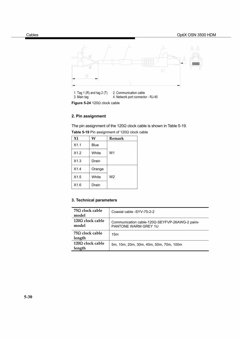
Cables OptiX OSN 3500 HDM
5-30
1. Tag 1 (R) and tag 2 (T) 2. Communication cable 3. Main tag 4. Network port connector - RJ-45
Figure 5-24 120Ω clock cable
2. Pin assignment
The pin assignment of the 120Ω clock cable is shown in Table 5-19. Table 5-19 Pin assignment of 120Ω clock cable
X1 W Remark X1.1 Blue
X1.2 White
X1.3 Drain
W1
X1.4 Orange
X1.5 White
X1.6 Drain
W2
3. Technical parameters
75Ω clock cable model
Coaxial cable -SYV-75-2-2
120Ω clock cable model
Communication cable-120Ω-SEYFVP-26AWG-2 pairs- PANTONE WARM GREY 1U
75Ω clock cable length
15m
120Ω clock cable length
5m, 10m, 20m, 30m, 40m, 50m, 70m, 100m
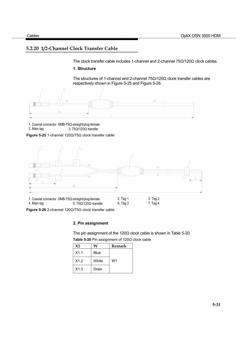
Cables OptiX OSN 3500 HDM
5-31
5.2.20 1/2-Channel Clock Transfer Cable
The clock transfer cable includes 1-channel and 2-channel 75Ω/120Ω clock cables.
1. Structure
The structures of 1-channel and 2-channel 75Ω/120Ω clock transfer cables are respectively shown in Figure 5-25 and Figure 5-26.
1. Coaxial connector -SMB-75Ω-straight/plug-female 2. Main tag 3. 75Ω/120Ω transfer
Figure 5-25 1-channel 120Ω/75Ω clock transfer cable
1. Coaxial connector -SMB-75Ω-straight/plug-female 2. Tag 1 3. Tag 2 4. Main tag 5. 75Ω/120Ω transfer 6. Tag 3 7. Tag 4
Figure 5-26 2-channel 120Ω/75Ω clock transfer cable
2. Pin assignment
The pin assignment of the 120Ω clock cable is shown in Table 5-20. Table 5-20 Pin assignment of 120Ω clock cable
X1 W Remark X1.1 Blue
X1.2 White
X1.3 Drain
W1
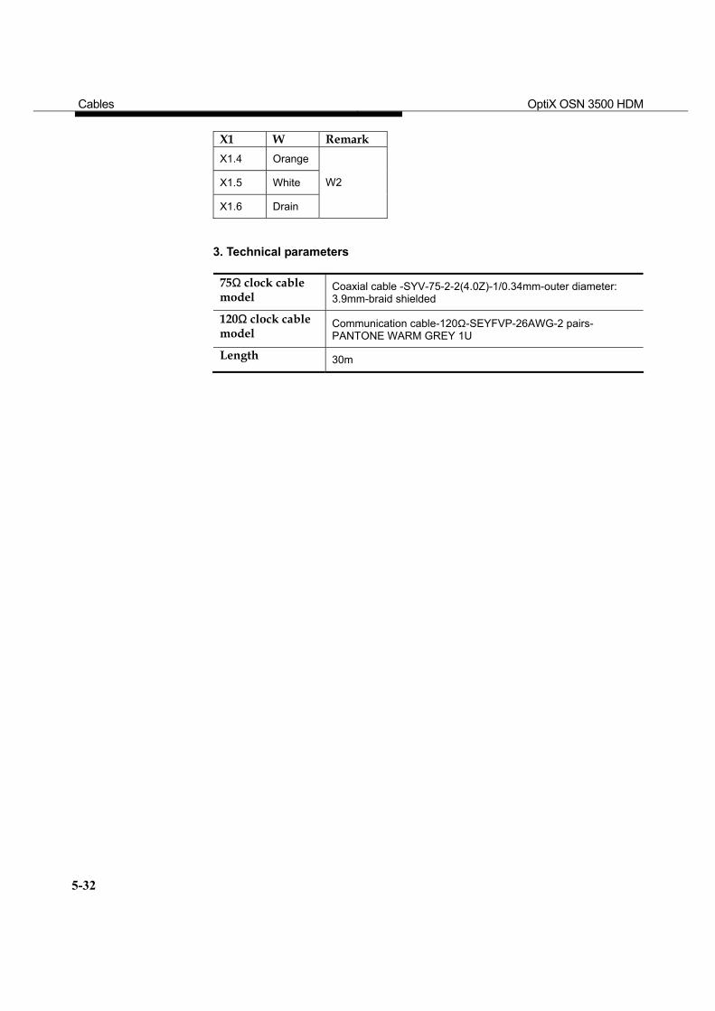
Cables OptiX OSN 3500 HDM
5-32
X1 W Remark X1.4 Orange
X1.5 White
X1.6 Drain
W2
3. Technical parameters
75Ω clock cable model
Coaxial cable -SYV-75-2-2(4.0Z)-1/0.34mm-outer diameter: 3.9mm-braid shielded
120Ω clock cable model
Communication cable-120Ω-SEYFVP-26AWG-2 pairs- PANTONE WARM GREY 1U
Length 30m
OptiX OSN 3500 HDM
A-1
A Indicator Description for
Equipment and Board
A.1 Cabinet Indicator Description
Indicator name Description On, the equipment power supply is normal. Normal power indicator (Power)
Off, the equipment power supply is exceptional.
On, critical alarm occurs to the equipment. Critical alarm indicator (Critical)
Off, no critical alarm occurs.
On, major alarm occurs to the equipment. Major alarm indicator (Major)
Off, no major alarm occurs.
On, minor alarm occurs to the equipment. Minor alarm indicator (Minor)
Off, no minor alarm occurs.
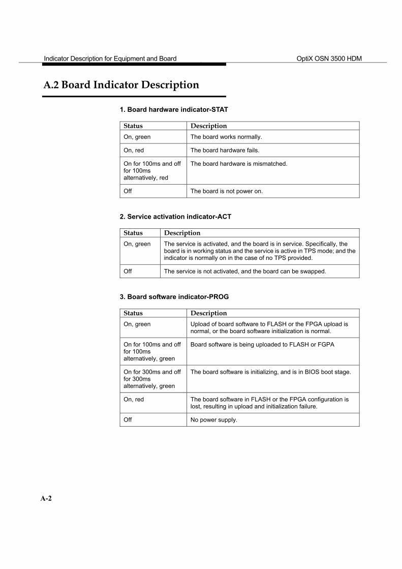
Indicator Description for Equipment and Board OptiX OSN 3500 HDM
A-2
A.2 Board Indicator Description
1. Board hardware indicator-STAT
Status Description On, green The board works normally.
On, red The board hardware fails.
On for 100ms and off for 100ms alternatively, red
The board hardware is mismatched.
Off The board is not power on.
2. Service activation indicator-ACT
Status Description On, green The service is activated, and the board is in service. Specifically, the
board is in working status and the service is active in TPS mode; and the indicator is normally on in the case of no TPS provided.
Off The service is not activated, and the board can be swapped.
3. Board software indicator-PROG
Status Description On, green Upload of board software to FLASH or the FPGA upload is
normal, or the board software initialization is normal.
On for 100ms and off for 100ms alternatively, green
Board software is being uploaded to FLASH or FGPA
On for 300ms and off for 300ms alternatively, green
The board software is initializing, and is in BIOS boot stage.
On, red The board software in FLASH or the FPGA configuration is lost, resulting in upload and initialization failure.
Off No power supply.
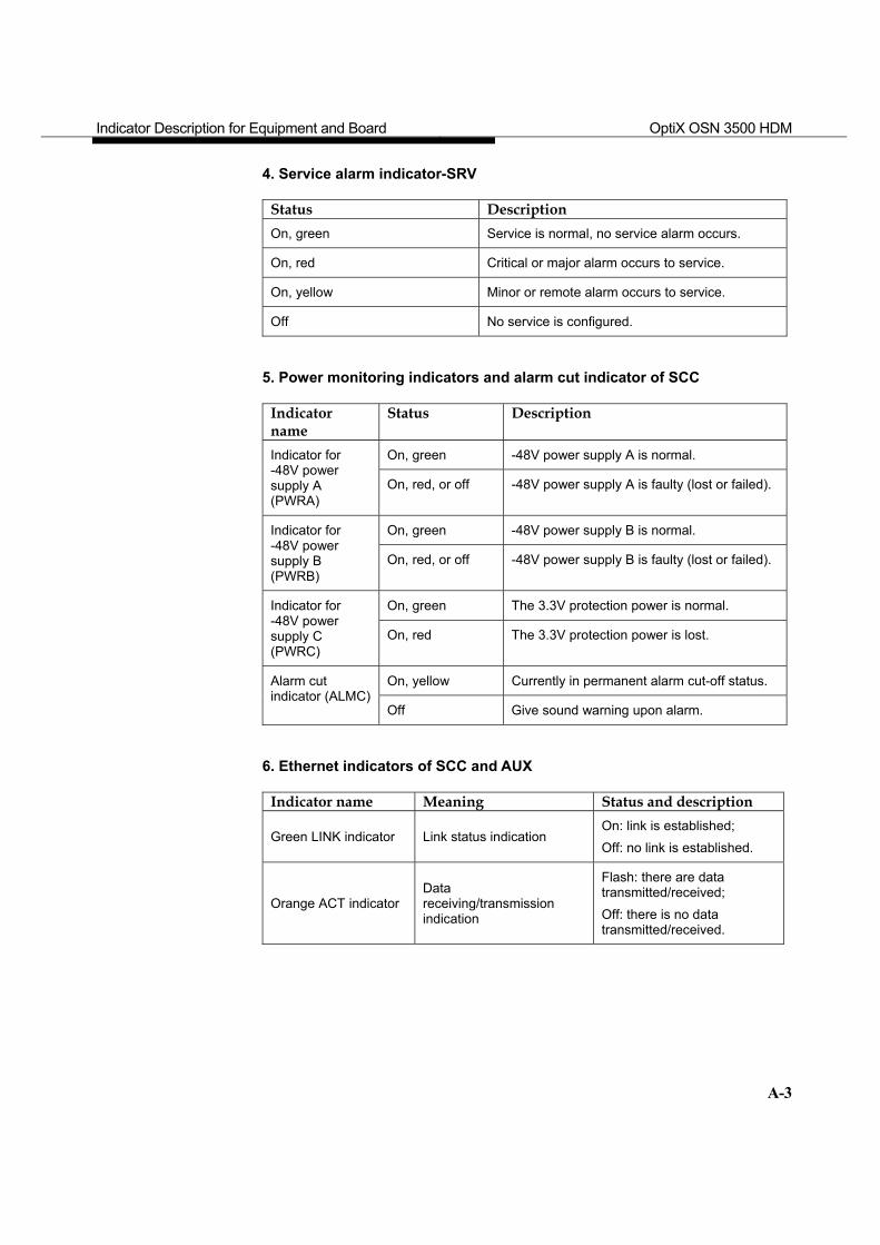
Indicator Description for Equipment and Board OptiX OSN 3500 HDM
A-3
4. Service alarm indicator-SRV
Status Description On, green Service is normal, no service alarm occurs.
On, red Critical or major alarm occurs to service.
On, yellow Minor or remote alarm occurs to service.
Off No service is configured.
5. Power monitoring indicators and alarm cut indicator of SCC
Indicator name
Status Description
On, green -48V power supply A is normal. Indicator for -48V power supply A (PWRA)
On, red, or off -48V power supply A is faulty (lost or failed).
On, green -48V power supply B is normal. Indicator for -48V power supply B (PWRB)
On, red, or off -48V power supply B is faulty (lost or failed).
On, green The 3.3V protection power is normal. Indicator for -48V power supply C (PWRC)
On, red The 3.3V protection power is lost.
On, yellow Currently in permanent alarm cut-off status. Alarm cut indicator (ALMC)
Off Give sound warning upon alarm.
6. Ethernet indicators of SCC and AUX
Indicator name Meaning Status and description
Green LINK indicator Link status indication On: link is established; Off: no link is established.
Orange ACT indicator Data receiving/transmission indication
Flash: there are data transmitted/received; Off: there is no data transmitted/received.
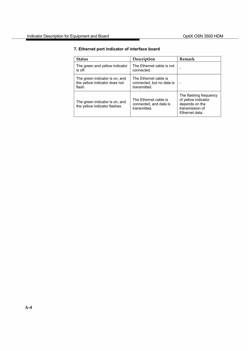
Indicator Description for Equipment and Board OptiX OSN 3500 HDM
A-4
7. Ethernet port indicator of interface board
Status Description Remark The green and yellow indicator is off.
The Ethernet cable is not connected. -
The green indicator is on, and the yellow indicator does not flash.
The Ethernet cable is connected, but no data is transmitted.
-
The green indicator is on, and the yellow indicator flashes.
The Ethernet cable is connected, and data is transmitted.
The flashing frequency of yellow indicator depends on the transmission of Ethernet data.
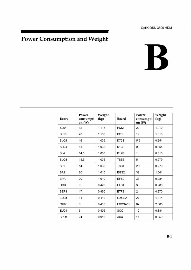
OptiX OSN 3500 HDM
B-1
B Power Consumption and Weight
Board Power consumption (W)
Weight (kg) Board
Power consumption (W)
Weight (kg)
SL64 32 1.118 PQM 22 1.010
SL16 20 1.100 PQ1 19 1.010
SLQ4 16 1.036 D75S 5.5 0.354
SLD4 15 1.032 D12S 9 0.354
SL4 14.5 1.030 D12B 1 0.310
SLQ1 15.5 1.036 TSB8 5 0.279
SL1 14 1.030 TSB4 2.5 0.279
BA2 20 1.010 EGS2 39 1.041
BPA 20 1.010 EFS0 33 0.984
DCU 0 0.420 EFS4 33 0.980
SEP1 17 0.950 ETF8 2 0.370
EU08 11 0.410 GXCSA 27 1.814
OU08 6 0.410 EXCSA/B 62 2.005
EU04 6 0.405 SCC 10 0.884
SPQ4 24 0.910 AUX 11 0.959

Power Consumption OptiX OSN 3500 HDM
B-2
Board Power consumption (W)
Weight (kg) Board
Power consumption (W)
Weight (kg)
MU04 2 0.405 AFB 0 1.230
PD3 19 1.120 FAN 30 1.5
PL3 15 0.995 PIU 8 1.151
D34S 2 0.381
C34S 2 0.310
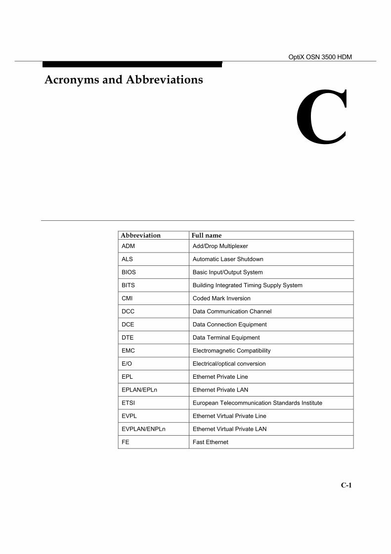
OptiX OSN 3500 HDM
C-1
C Acronyms and Abbreviations
Abbreviation Full name ADM Add/Drop Multiplexer
ALS Automatic Laser Shutdown
BIOS Basic Input/Output System
BITS Building Integrated Timing Supply System
CMI Coded Mark Inversion
DCC Data Communication Channel
DCE Data Connection Equipment
DTE Data Terminal Equipment
EMC Electromagnetic Compatibility
E/O Electrical/optical conversion
EPL Ethernet Private Line
EPLAN/EPLn Ethernet Private LAN
ETSI European Telecommunication Standards Institute
EVPL Ethernet Virtual Private Line
EVPLAN/ENPLn Ethernet Virtual Private LAN
FE Fast Ethernet
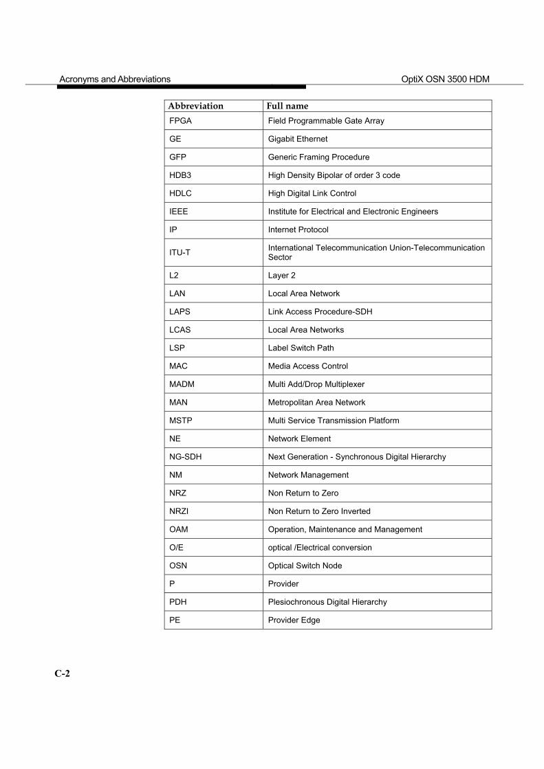
Acronyms and Abbreviations OptiX OSN 3500 HDM
C-2
Abbreviation Full name FPGA Field Programmable Gate Array
GE Gigabit Ethernet
GFP Generic Framing Procedure
HDB3 High Density Bipolar of order 3 code
HDLC High Digital Link Control
IEEE Institute for Electrical and Electronic Engineers
IP Internet Protocol
ITU-T International Telecommunication Union-Telecommunication Sector
L2 Layer 2
LAN Local Area Network
LAPS Link Access Procedure-SDH
LCAS Local Area Networks
LSP Label Switch Path
MAC Media Access Control
MADM Multi Add/Drop Multiplexer
MAN Metropolitan Area Network
MSTP Multi Service Transmission Platform
NE Network Element
NG-SDH Next Generation - Synchronous Digital Hierarchy
NM Network Management
NRZ Non Return to Zero
NRZI Non Return to Zero Inverted
OAM Operation, Maintenance and Management
O/E optical /Electrical conversion
OSN Optical Switch Node
P Provider
PDH Plesiochronous Digital Hierarchy
PE Provider Edge
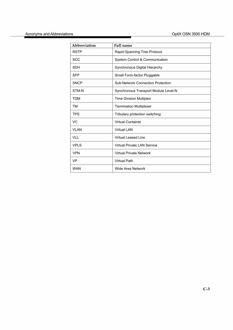
Acronyms and Abbreviations OptiX OSN 3500 HDM
C-3
Abbreviation Full name RSTP Rapid Spanning Tree Protocol
SCC System Control & Communication
SDH Synchronous Digital Hierarchy
SFP Small Form-factor Pluggable
SNCP Sub-Network Connection Protection
STM-N Synchronous Transport Module Level-N
TDM Time Division Multiplex
TM Termination Multiplexer
TPS Tributary protection switching
VC Virtual Container
VLAN Virtual LAN
VLL Virtual Leased Line
VPLS Virtual Private LAN Service
VPN Virtual Private Network
VP Virtual Path
WAN Wide Area Network
Related Documents