1024-/256-Position, 1% Resistor Tolerance Error, I 2 C Interface and 50-TP Memory Digital Rheostat Data Sheet AD5272/AD5274 Rev. D Document Feedback Information furnished by Analog Devices is believed to be accurate and reliable. However, no responsibility is assumed by Analog Devices for its use, nor for any infringements of patents or other rights of third parties that may result from its use. Specifications subject to change without notice. No license is granted by implication or otherwise under any patent or patent rights of Analog Devices. Trademarks and registered trademarks are the property of their respective owners. One Technology Way, P.O. Box 9106, Norwood, MA 02062-9106, U.S.A. Tel: 781.329.4700 ©2009–2013 Analog Devices, Inc. All rights reserved. Technical Support www.analog.com FEATURES Single-channel, 1024-/256-position resolution 20 kΩ, 50 kΩ, 100 kΩ nominal resistance Maximum ±1% nominal resistor tolerance error 50-times programmable (50-TP) wiper memory Rheostat mode temperature coefficient: 5 ppm/°C 2.7 V to 5.5 V single-supply operation ±2.5 V to ±2.75 V dual-supply operation for ac or bipolar operations I 2 C-compatible interface Wiper setting readback Power on refreshed from 50-TP memory Thin LFCSP 10-lead, 3 mm × 3 mm × 0.8 mm package Compact MSOP, 10-lead 3 mm × 4.9 mm × 1.1 mm package APPLICATIONS Mechanical rheostat replacements Op-amp: variable gain control Instrumentation: gain, offset adjustment Programmable voltage to current conversions Programmable filters, delays, time constants Programmable power supply Sensor calibration FUNCTIONAL BLOCK DIAGRAM 10/8 V DD A W AD5272/AD5274 SCL ADDR SDA I 2 C SERIAL INTERFACE POWER-ON RESET RDAC REGISTER 50-TP MEMORY BLOCK RESET V SS EXT_CAP GND 08076-001 Figure 1. GENERAL DESCRIPTION The AD5272/AD5274 1 are single-channel, 1024-/256-position digital rheostats that combine industry leading variable resistor performance with nonvolatile memory (NVM) in a compact package. The AD5272/AD5274 ensure less than 1% end-to-end resistor tolerance error and offer 50-times programmable (50-TP) memory. The guaranteed industry leading low resistor tolerance error feature simplifies open-loop applications as well as precision calibration and tolerance matching applications. The AD5272/AD5274 device wiper settings are controllable through the I 2 C-compatible digital interface. Unlimited adjustments are allowed before programming the resistance value into the 50-TP memory. The AD5272/AD5274 do not require any external voltage supply to facilitate fuse blow and there are 50 opportunities for permanent programming. During 50-TP activation, a permanent blow fuse command freezes the wiper position (analogous to placing epoxy on a mechanical trimmer). The AD5272/AD5274 are available in a 3 mm × 3 mm 10-lead LFCSP package and in a 10-lead MSOP package. The parts are guaranteed to operate over the extended industrial temperature range of −40°C to +125°C. 1 Protected by U.S. Patent Number 7688240.

Welcome message from author
This document is posted to help you gain knowledge. Please leave a comment to let me know what you think about it! Share it to your friends and learn new things together.
Transcript

1024-/256-Position, 1% Resistor Tolerance Error,I2C Interface and 50-TP Memory Digital Rheostat
Data Sheet AD5272/AD5274
Rev. D Document Feedback Information furnished by Analog Devices is believed to be accurate and reliable. However, no responsibility is assumed by Analog Devices for its use, nor for any infringements of patents or other rights of third parties that may result from its use. Specifications subject to change without notice. No license is granted by implication or otherwise under any patent or patent rights of Analog Devices. Trademarks and registered trademarks are the property of their respective owners.
One Technology Way, P.O. Box 9106, Norwood, MA 02062-9106, U.S.A.Tel: 781.329.4700 ©2009–2013 Analog Devices, Inc. All rights reserved. Technical Support www.analog.com
FEATURES Single-channel, 1024-/256-position resolution 20 kΩ, 50 kΩ, 100 kΩ nominal resistance Maximum ±1% nominal resistor tolerance error 50-times programmable (50-TP) wiper memory Rheostat mode temperature coefficient: 5 ppm/°C 2.7 V to 5.5 V single-supply operation ±2.5 V to ±2.75 V dual-supply operation for ac or bipolar
operations I2C-compatible interface Wiper setting readback Power on refreshed from 50-TP memory Thin LFCSP 10-lead, 3 mm × 3 mm × 0.8 mm package Compact MSOP, 10-lead 3 mm × 4.9 mm × 1.1 mm package
APPLICATIONS Mechanical rheostat replacements Op-amp: variable gain control Instrumentation: gain, offset adjustment Programmable voltage to current conversions Programmable filters, delays, time constants Programmable power supply Sensor calibration
FUNCTIONAL BLOCK DIAGRAM
10/8
VDD
A
W
AD5272/AD5274
SCL
ADDR
SDAI2C
SERIALINTERFACE
POWER-ONRESET
RDACREGISTER
50-TPMEMORYBLOCK
RESET
VSS EXT_CAP GND
0807
6-00
1
Figure 1.
GENERAL DESCRIPTION The AD5272/AD52741 are single-channel, 1024-/256-position digital rheostats that combine industry leading variable resistor performance with nonvolatile memory (NVM) in a compact package.
The AD5272/AD5274 ensure less than 1% end-to-end resistor tolerance error and offer 50-times programmable (50-TP) memory.
The guaranteed industry leading low resistor tolerance error feature simplifies open-loop applications as well as precision calibration and tolerance matching applications.
The AD5272/AD5274 device wiper settings are controllable through the I2C-compatible digital interface. Unlimited adjustments are allowed before programming the resistance value into the 50-TP memory. The AD5272/AD5274 do not require any external voltage supply to facilitate fuse blow and there are 50 opportunities for permanent programming. During 50-TP activation, a permanent blow fuse command freezes the wiper position (analogous to placing epoxy on a mechanical trimmer).
The AD5272/AD5274 are available in a 3 mm × 3 mm 10-lead LFCSP package and in a 10-lead MSOP package. The parts are guaranteed to operate over the extended industrial temperature range of −40°C to +125°C.
1 Protected by U.S. Patent Number 7688240.

AD5272/AD5274 Data Sheet
Rev. D | Page 2 of 28
TABLE OF CONTENTS Features .............................................................................................. 1 Applications ....................................................................................... 1 Functional Block Diagram .............................................................. 1 General Description ......................................................................... 1 Revision History ............................................................................... 2 Specifications ..................................................................................... 3
Electrical Characteristics—AD5272 .......................................... 3 Electrical Characteristics—AD5274 .......................................... 5 Interface Timing Specifications .................................................. 7
Absolute Maximum Ratings ............................................................ 9 Thermal Resistance ...................................................................... 9 ESD Caution .................................................................................. 9
Pin Configuration and Function Descriptions ........................... 10 Typical Performance Characteristics ........................................... 11 Test Circuits ..................................................................................... 17 Theory of Operation ...................................................................... 18
Serial Data Interface ................................................................... 18
Shift Register ............................................................................... 18 Write Operation.......................................................................... 19 Read Operation........................................................................... 20 RDAC Register ............................................................................ 21 50-TP Memory Block ................................................................ 21 Write Protection ......................................................................... 21 50-TP Memory Write-Acknowledge Polling .......................... 23 Reset ............................................................................................. 23 Resistor Performance Mode ...................................................... 23 Shutdown Mode ......................................................................... 23 RDAC Architecture .................................................................... 23 Programming the Variable Resistor ......................................... 23 EXT_CAP Capacitor .................................................................. 24 Terminal Voltage Operating Range ......................................... 24 Power-Up Sequence ................................................................... 24
Outline Dimensions ....................................................................... 25 Ordering Guide .......................................................................... 25
REVISION HISTORY 3/13—Rev. C to Rev. D Changed Resistor Noise Density, RAW = 20 kΩ from 50 nV/√Hz to 13 nV/√Hz; Table 1 ...................................................................... 4 Changed Resistor Noise Density, RAW = 20 kΩ from 50 nV/√Hz to 13 nV/√Hz; Table 4 ...................................................................... 6 Updated Outline Dimensions ....................................................... 25 11/10—Rev. B to Rev. C Changes to Figure 24 ...................................................................... 14 5/10—Rev. A to Rev. B Added LFCSP Package .................................................. Throughout Changed OTP to 50-TP ................................................ Throughout Changes to Features Section and Applications Section ............... 1 Added Endnote 1 .............................................................................. 1 Changes to Table 1 ............................................................................ 3 Added Table 3 .................................................................................... 4 Changes to Table 4 ............................................................................ 5 Added Table 6 .................................................................................... 6 Changes to Table 8 and Table 9 ....................................................... 9 Added Figure 5 ................................................................................ 10 Added Exposed Pad Note to Table 10 .......................................... 10 Changes to Typical Performance Characteristics ....................... 11 Changes to Resistor Performance Mode Section ....................... 23 Updated Outline Dimensions ....................................................... 25 Changes to Ordering Guide .......................................................... 26
3/10—Rev. 0 to Rev. A Changes to Product Title and General Description Section ....... 1 Changes to Theory of Operation Section.................................... 15 10/09—Revision 0: Initial Version

Data Sheet AD5272/AD5274
Rev. D | Page 3 of 28
SPECIFICATIONS ELECTRICAL CHARACTERISTICS—AD5272 VDD = 2.7 V to 5.5 V, VSS = 0 V; VDD = 2.5 V to 2.75 V, VSS = −2.5 V to −2.75 V; −40°C < TA < +125°C, unless otherwise noted.
Table 1. Parameter Symbol Test Conditions/Comments Min Typ1 Max Unit DC CHARACTERISTICS—RHEOSTAT MODE
Resolution 10 Bits Resistor Integral Nonlinearity2, 3 R-INL RAW= 20 kΩ, |VDD − VSS| = 3.0 V to 5.5 V −1 +1 LSB RAW= 20 kΩ, |VDD − VSS| = 2.7 V to 3.0 V −1 +1.5 LSB
RAW= 50 kΩ, 100 kΩ −1 +1 LSB Resistor Differential Nonlinearity2 R-DNL −1 +1 LSB Nominal Resistor Tolerance
R-Perf Mode4 See Table 2 and Table 3 −1 ±0.5 +1 % Normal Mode ±15 %
Resistance Temperature Coefficient5, 6 Code = full scale 5 ppm/°C Wiper Resistance Code = zero scale 35 70 Ω
RESISTOR TERMINALS Terminal Voltage Range5, 7 VSS VDD V Capacitance5 A f = 1 MHz, measured to GND, code = half scale 90 pF Capacitance5 W f = 1 MHz, measured to GND, code = half scale 40 pF Common-Mode Leakage Current5 VA = VW 50 nA
DIGITAL INPUTS Input Logic5
High VINH 2.0 V Low VINL 0.8 V
Input Current IIN ±1 µA Input Capacitance5 CIN 5 pF
DIGITAL OUTPUT Output Voltage5
High VOH RPULL_UP = 2.2 kΩ to VDD VDD − 0.1 V Low VOL RPULL_UP = 2.2 kΩ to VDD
VDD = 2.7 V to 5.5 V, VSS = 0 V 0.4 V VDD = 2.5 V to 2.75 V, VSS = −2.5 V to −2.75 V 0.6 V Tristate Leakage Current −1 +1 µA Output Capacitance5 5 pF
POWER SUPPLIES Single-Supply Power Range VSS = 0 V 2.7 5.5 V Dual-Supply Power Range ±2.5 ±2.75 V Supply Current
Positive IDD 1 µA Negative ISS −1 µA
50-TP Store Current5, 8 Positive IDD_OTP_STORE 4 mA Negative ISS_OTP_STORE −4 mA
50-TP Read Current5, 9 Positive IDD_OTP_READ 500 µA Negative ISS_OTP_READ −500 µA
Power Dissipation10 VIH = VDD or VIL = GND 5.5 µW
AD5272/AD5274 Data Sheet
Rev. D | Page 4 of 28
Parameter Symbol Test Conditions/Comments Min Typ1 Max Unit Power Supply Rejection Ratio5 PSRR ΔVDD/ΔVSS = ±5 V ± 10% dB RAW = 20 kΩ −66 −55 RAW = 50 kΩ −75 −67 RAW = 100 kΩ −78 −70
DYNAMIC CHARACTERISTICS5, 11 Bandwidth −3 dB, RAW = 10 kΩ, Terminal W, see Figure 41 kHz RAW = 20 kΩ 300 RAW = 50 kΩ 120 RAW = 100 kΩ 60 Total Harmonic Distortion VA = 1 V rms, f = 1 kHz, code = half scale dB RAW = 20 kΩ −90 RAW = 50 kΩ −88 RAW = 100 kΩ −85 Resistor Noise Density Code = half scale, TA = 25°C, f = 10 kHz nV/√Hz RAW = 20 kΩ 13 RAW = 50 kΩ 25 RAW = 100 kΩ 32
1 Typical specifications represent average readings at 25°C, VDD = 5 V, and VSS = 0 V. 2 Resistor position nonlinearity error (R-INL) is the deviation from an ideal value measured between the maximum resistance and the minimum resistance wiper
positions. R-DNL measures the relative step change from ideal between successive tap positions. 3 The maximum current in each code is defined by IAW = (VDD − 1)/RAW. 4 The terms, resistor performance mode and R-Perf mode, are used interchangeably. See the Resistor Performance Mode section. 5 Guaranteed by design and not subject to production test. 6 See Figure 24 for more details. 7 Resistor Terminal A and Resistor Terminal W have no limitations on polarity with respect to each other. Dual-supply operation enables ground referenced bipolar
signal adjustment. 8 Different from operating current, the supply current for the fuse program lasts approximately 55 ms. 9 Different from operating current, the supply current for the fuse read lasts approximately 500 ns. 10 PDISS is calculated from (IDD × VDD) + (ISS × VSS). 11 All dynamic characteristics use VDD = +2.5 V, VSS = −2.5 V.
Table 2. AD5272 Resistor Performance Mode Code Range Resistor Tolerance Per Code |VDD − VSS| = 4.5 V to 5.5 V |VDD − VSS| = 2.7 V to 4.5 V R-TOLERANCE
1% R-Tolerance From 0x078 to 0x3FF From 0x0BE to 0x3FF 2% R-Tolerance From 0x037 to 0x3FF From 0x055 to 0x3FF 3% R-Tolerance From 0x028 to 0x3FF From 0x037 to 0x3FF
Table 3. AD5272 50 kΩ and 100 kΩ Resistor Performance Mode Code Range Resistor Tolerance Per Code RAW = 50 kΩ RAW = 100 kΩ R-TOLERANCE
1% R-Tolerance From 0x078 to 0x3FF From 0x04B to 0x3FF 2% R-Tolerance From 0x055 to 0x3FF From 0x032 to 0x3FF 3% R-Tolerance From 0x032 to 0x3FF From 0x019 to 0x3FF

Data Sheet AD5272/AD5274
Rev. D | Page 5 of 28
ELECTRICAL CHARACTERISTICS—AD5274 VDD = 2.7 V to 5.5 V, VSS = 0 V; VDD = 2.5 V to 2.75 V, VSS = −2.5 V to −2.75 V; −40°C < TA < +125°C, unless otherwise noted.
Table 4. Parameter Symbol Test Conditions/Comments Min Typ1 Max Unit DC CHARACTERISTICS—
RHEOSTAT MODE
Resolution 8 Bits Resistor Integral Nonlinearity2, 3 R-INL −1 +1 LSB Resistor Differential
Nonlinearity2 R-DNL −1 +1 LSB
Nominal Resistor Tolerance R-Perf Mode4 See Table 5 and Table 6 −1 ±0.5 +1 % Normal Mode ±15 %
Resistance Temperature Coefficient5, 6
Code = full scale 5 ppm/°C
Wiper Resistance Code = zero scale 35 70 Ω RESISTOR TERMINALS
Terminal Voltage Range5, 7 VSS VDD V Capacitance5 A f = 1 MHz, measured to GND, code = half scale 90 pF Capacitance5 W f = 1 MHz, measured to GND, code = half scale 40 pF Common-Mode Leakage
Current5 VA = VW 50 nA
DIGITAL INPUTS Input Logic5
High VINH 2.0 V Low VINL 0.8 V
Input Current IIN ±1 µA Input Capacitance5 CIN 5 pF
DIGITAL OUTPUT Output Voltage5
High VOH RPULL_UP = 2.2 kΩ to VDD VDD − 0.1 V Low VOL RPULL_UP = 2.2 kΩ to VDD
VDD = 2.7 V to 5.5 V, VSS = 0 V 0.4 V VDD = 2.5 V to 2.75 V, VSS = −2.5 V to −2.75 V 0.6 V Tristate Leakage Current −1 +1 µA Output Capacitance5 5 pF
POWER SUPPLIES Single-Supply Power Range VSS = 0 V 2.7 5.5 V Dual-Supply Power Range ±2.5 ±2.75 V Supply Current
Positive IDD 1 µA Negative ISS −1 µA
OTP Store Current5, 8 Positive IDD_OTP_STORE 4 mA Negative ISS_OTP_STORE −4 mA
OTP Read Current5, 9 Positive IDD_OTP_READ 500 µA Negative ISS_OTP_READ −500 µA
Power Dissipation10 VIH = VDD or VIL = GND 5.5 µW Power Supply Rejection Ratio5 PSRR ΔVDD/ΔVSS = ±5 V ± 10% dB RAW = 20 kΩ −66 −55 RAW = 50 kΩ −75 −67 RAW = 100 kΩ −78 −70

AD5272/AD5274 Data Sheet
Rev. D | Page 6 of 28
Parameter Symbol Test Conditions/Comments Min Typ1 Max Unit DYNAMIC CHARACTERISTICS5, 11
Bandwidth −3 dB, RAW = 10 kΩ, Terminal W, see Figure 41 kHz RAW = 20 kΩ 300 RAW = 50 kΩ 120 RAW = 100 kΩ 60 Total Harmonic Distortion VA = 1 V rms, f = 1 kHz, code = half scale dB RAW = 20 kΩ −90 RAW = 50 kΩ −88 RAW = 100 kΩ −85 Resistor Noise Density Code = half scale, TA = 25°C, f = 10 kHz nV/√Hz RAW = 20 kΩ 13 RAW = 50 kΩ 25 RAW = 100 kΩ 32
1 Typical specifications represent average readings at 25°C, VDD = 5 V, and VSS = 0 V. 2 Resistor position nonlinearity error (R-INL) is the deviation from an ideal value measured between the maximum resistance and the minimum resistance wiper
positions. R-DNL measures the relative step change from ideal between successive tap positions. 3 The maximum current in each code is defined by IAW = (VDD − 1)/RAW. 4 The terms, resistor performance mode and R-Perf mode, are used interchangeably. See the Resistor Performance Mode section. 5 Guaranteed by design and not subject to production test. 6 See Figure 24 for more details. 7 Resistor Terminal A and Resistor Terminal W have no limitations on polarity with respect to each other. Dual-supply operation enables ground referenced bipolar
signal adjustment. 8 Different from operating current, the supply current for the fuse program lasts approximately 55 ms. 9 Different from operating current, the supply current for the fuse read lasts approximately 500 ns. 10 PDISS is calculated from (IDD × VDD) + (ISS × VSS). 11 All dynamic characteristics use VDD = +2.5 V, VSS = −2.5 V.
Table 5. AD5274 Resistor Performance Mode Code Range Resistor Tolerance per Code |VDD − VSS| = 4.5 V to 5.5 V |VDD − VSS| = 2.7 V to 4.5 V R-TOLERANCE
1% R-Tolerance From 0x1E to 0xFF From 0x32 to 0xFF 2% R-Tolerance From 0x0F to 0xFF From 0x19 to 0xFF 3% R-Tolerance From 0x06 to 0xFF From 0x0E to 0xFF
Table 6. AD5274 50 kΩ and 100 kΩ Resistor Performance Mode Code Range Resistor Tolerance per Code RAW = 50 kΩ RAW = 100 kΩ R-TOLERANCE
1% R-Tolerance From 0x1E to 0xFF From 0x14 to 0xFF 2% R-Tolerance From 0x14 to 0xFF From 0x0F to 0xFF 3% R-Tolerance From 0x0A to 0xFF From 0x0A to 0xFF
Data Sheet AD5272/AD5274
Rev. D | Page 7 of 28
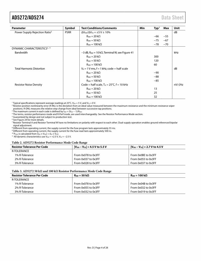
INTERFACE TIMING SPECIFICATIONS VDD = 2.5 V to 5.5 V; all specifications TMIN to TMAX, unless otherwise noted.
Table 7. Limit at TMIN, TMAX Parameter Conditions1 Min Max Unit Description fSCL
2 Standard mode 100 kHz Serial clock frequency Fast mode 400 kHz Serial clock frequency t1 Standard mode 4 µs tHIGH, SCL high time Fast mode 0.6 µs tHIGH, SCL high time t2 Standard mode 4.7 µs tLOW, SCL low time Fast mode 1.3 µs tLOW, SCL low time t3 Standard mode 250 ns tSU;DAT, data setup time Fast mode 100 ns tSU;DAT, data setup time t4 Standard mode 0 3.45 µs tHD;DAT, data hold time Fast mode 0 0.9 µs tHD;DAT, data hold time t5 Standard mode 4.7 µs tSU;STA, set-up time for a repeated start condition Fast mode 0.6 µs tSU;STA, set-up time for a repeated start condition t6 Standard mode 4 µs tHD;STA, hold time (repeated) start condition Fast mode 0.6 µs tHD;STA, hold time (repeated) start condition High speed mode 160 ns tHD;STA, hold time (repeated) start condition t7 Standard mode 4.7 µs tBUF, bus free time between a stop and a start condition Fast mode 1.3 µs tBUF, bus free time between a stop and a start condition t8 Standard mode 4 µs tSU;STO, setup time for a stop condition Fast mode 0.6 µs tSU;STO, setup time for a stop condition t9 Standard mode 1000 ns tRDA, rise time of SDA signal Fast mode 300 ns tRDA, rise time of SDA signal t10 Standard mode 300 ns tFDA, fall time of SDA signal Fast mode 300 ns tFDA, fall time of SDA signal t11 Standard mode 1000 ns tRCL, rise time of SCL signal Fast mode 300 ns tRCL, rise time of SCL signal t11A Standard mode 1000 ns tRCL1, rise time of SCL signal after a repeated start condition and
after an acknowledge bit Fast mode 300 ns tRCL1, rise time of SCL signal after a repeated start condition and
after an acknowledge bit t12 Standard mode 300 ns tFCL, fall time of SCL signal Fast mode 300 ns tFCL, fall time of SCL signal t13 RESET pulse time 20 ns Minimum RESET low time
tSP3 Fast mode 0 50 ns Pulse width of spike suppressed
tEXEC4, 5 500 ns Command execute time
tRDAC_R-PERF 2 µs RDAC register write command execute time (R-Perf mode) tRDAC_NORMAL 600 ns RDAC register write command execute time (normal mode) tMEMORY_READ 6 µs Memory readback execute time tMEMORY_PROGRAM 350 ms Memory program time tRESET 600 µs Reset 50-TP restore time tPOWER-UP
6 2 ms Power-on 50-TP restore time 1 Maximum bus capacitance is limited to 400 pF. 2 The SDA and SCL timing is measured with the input filters enabled. Switching off the input filters improves the transfer rate but has a negative effect on EMC behavior
of the part. 3 Input filtering on the SCL and SDA inputs suppress noise spikes that are less than 50 ns for fast mode. 4 Refer to tRDAC_R-PERF and tRDAC_NORMAL for RDAC register write operations. 5 Refer to tMEMORY_READ and tMEMORY_PROGRAM for memory commands operations. 6 Maximum time after VDD − VSS is equal to 2.5 V.

AD5272/AD5274 Data Sheet
Rev. D | Page 8 of 28
Shift Register and Timing Diagrams
DATA BITS
DB9 (MSB) DB0 (LSB)
D7 D6 D5 D4 D3 D2 D1 D0
CONTROL BITS
C0 C1 C2 D9 D8 C3 0 0
0807
6-00
3
Figure 2. Shift Register Content
0807
6-00
2
RESET
t7
t6
t2
t4
t11 t12 t6
t5t10
t1
SCL
SDA
P S S P
t3
t8
t9
t13
Figure 3. 2-Wire Serial Interface Timing Diagram
Data Sheet AD5272/AD5274
Rev. D | Page 9 of 28
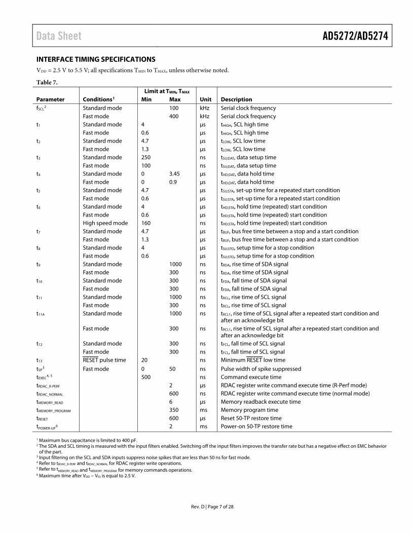
ABSOLUTE MAXIMUM RATINGS TA = 25°C, unless otherwise noted.
Table 8. Parameter Rating VDD to GND –0.3 V to +7.0 V VSS to GND +0.3 V to −7.0 V VDD to VSS 7 V VA, VW to GND VSS − 0.3 V, VDD + 0.3 V Digital Input and Output Voltage to GND −0.3 V to VDD + 0.3 V EXT_CAP to VSS 7 V IA, IW
Continuous RAW = 20 kΩ ±3 mA RAW = 50 kΩ, 100 kΩ ±2 mA
Pulsed1 Frequency > 10 kHz ±MCC2/d3 Frequency ≤ 10 kHz ±MCC2/√d3
Operating Temperature Range4 −40°C to +125°C Maximum Junction Temperature
(TJ Maximum) 150°C
Storage Temperature Range −65°C to +150°C Reflow Soldering
Peak Temperature 260°C Time at Peak Temperature 20 sec to 40 sec
Package Power Dissipation (TJ max − TA)/θJA 1 Maximum terminal current is bounded by the maximum current handling of
the switches, maximum power dissipation of the package, and maximum applied voltage across any two of the A and W terminals at a given resistance.
2 Maximum continuous current 3 Pulse duty factor. 4 Includes programming of 50-TP memory.
Stresses above those listed under Absolute Maximum Ratings may cause permanent damage to the device. This is a stress rating only and functional operation of the device at these or any other conditions above those indicated in the operational section of this specification is not implied. Exposure to absolute maximum rating conditions for extended periods may affect device reliability.
THERMAL RESISTANCE θJA is defined by JEDEC specification JESD-51 and the value is dependent on the test board and test environment.
Table 9. Thermal Resistance Package Type θJA
1 θJC Unit 10-Lead LFCSP 50 3 °C/W 10-Lead MSOP 135 N/A °C/W 1 JEDEC 2S2P test board, still air (0 m/s air flow).
ESD CAUTION
AD5272/AD5274 Data Sheet
Rev. D | Page 10 of 28
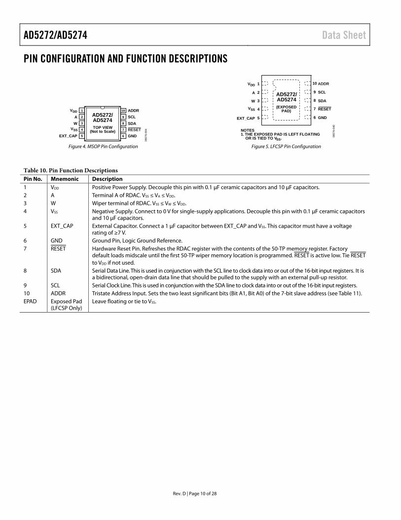
PIN CONFIGURATION AND FUNCTION DESCRIPTIONS
VDD 1
VSS
2A3W4
10
9
8
SCLADDR
7
5EXT_CAP
SDA
6 GND
AD5272/AD5274TOP VIEW
(Not to Scale) RESET
0807
6-00
4
Figure 4. MSOP Pin Configuration
ADDRVDD 1
VSS
2A
3W
4 RESET
10
9
8
SCL
7
5EXT_CAP
SDA
6 GND
NOTES1. THE EXPOSED PAD IS LEFT FLOATING OR IS TIED TO VSS.
AD5272/AD5274(EXPOSED
PAD)
0807
6-04
0
Figure 5. LFCSP Pin Configuration
Table 10. Pin Function Descriptions Pin No. Mnemonic Description 1 VDD Positive Power Supply. Decouple this pin with 0.1 μF ceramic capacitors and 10 μF capacitors. 2 A Terminal A of RDAC. VSS ≤ VA ≤ VDD. 3 W Wiper terminal of RDAC. VSS ≤ VW ≤ VDD. 4 VSS Negative Supply. Connect to 0 V for single-supply applications. Decouple this pin with 0.1 μF ceramic capacitors
and 10 μF capacitors. 5 EXT_CAP External Capacitor. Connect a 1 μF capacitor between EXT_CAP and VSS. This capacitor must have a voltage
rating of ≥7 V. 6 GND Ground Pin, Logic Ground Reference. 7 RESET Hardware Reset Pin. Refreshes the RDAC register with the contents of the 50-TP memory register. Factory
default loads midscale until the first 50-TP wiper memory location is programmed. RESET is active low. Tie RESET to VDD if not used.
8 SDA Serial Data Line. This is used in conjunction with the SCL line to clock data into or out of the 16-bit input registers. It is a bidirectional, open-drain data line that should be pulled to the supply with an external pull-up resistor.
9 SCL Serial Clock Line. This is used in conjunction with the SDA line to clock data into or out of the 16-bit input registers. 10 ADDR Tristate Address Input. Sets the two least significant bits (Bit A1, Bit A0) of the 7-bit slave address (see Table 11). EPAD Exposed Pad
(LFCSP Only) Leave floating or tie to VSS.

Data Sheet AD5272/AD5274
Rev. D | Page 11 of 28
TYPICAL PERFORMANCE CHARACTERISTICS
–0.4
–0.2
0
0.2
0.4
0.6
0.8
0 128 256 384 512 640 768 896 1023
INL
(LSB
)
CODE (Decimal)
+125°C+25°C–40°C
0807
6-01
0
RAW = 20kΩ
Figure 6. R-INL in R-Perf Mode vs. Code vs. Temperature (AD5272)
CODE (Decimal)
DN
L (L
SB)
0807
6-01
1–0.6
–0.5
–0.4
–0.3
–0.2
–0.1
0
0.1
0.2
0 128 256 384 512 640 768 896 1023
+25°C–40°C +125°C
RAW = 20kΩ
Figure 7. R-DNL in R-Perf Mode vs. Code vs. Temperature (AD5272)
–0.1
0
0.1
0.4
0.2
0.3
0.5
INL
(LSB
)
CODE (Decimal)0 128 256 384 512 640 768 896 1023
+125°C+25°C–40°C
0807
6-01
4
RAW = 20kΩ
Figure 8. R-INL in Normal Mode vs. Code vs. Temperature (AD5272)
0.8
0.6
0.4
0.2
0
–0.2
–0.40 256 512 768 1023
CODE (Decimal)
INL
(LSB
)
0807
6-11
1
20kΩ50kΩ100kΩ
TA = 25°C
Figure 9. R-INL in R-Perf Mode vs. Code vs. Nominal Resistance (AD5272)
0 256 512 768 1023CODE (Decimal)
0.6
0.4
0.2
0
–0.2
–0.4
–0.6
DN
L (L
SB)
0807
6-12
0
20kΩ 50kΩ 100kΩ
TA = 25°C
Figure 10. R-DNL in R-Perf Mode vs. Code vs. Nominal Resistance (AD5272)
0 256 512 768 1023CODE (Decimal)
0.4
0.6
0.2
0
–0.2
–0.4
INL
(LSB
)
0807
6-12
1
20kΩ50kΩ100kΩ
TA = 25°C
Figure 11. R-INL in Normal Mode vs. Code vs. Nominal Resistance (AD5272)

AD5272/AD5274 Data Sheet
Rev. D | Page 12 of 28
–0.15
–0.10
–0.05
0.10
0
0.05
0.15
DN
L (L
SB)
CODE (Decimal)0 128 256 384 512 640 768 896 1023
+125°C+25°C–40°C
0807
6-01
5
RAW = 20kΩ
Figure 12. R-DNL in Normal Mode vs. Code vs. Temperature (AD5272)
CODE (Decimal)0 64 128 192 255
–0.10
–0.05
0
0.15
0.05
0.10
0.20
INL
(LSB
)
+125°C+25°C–40°C
0807
6-01
3
RAW = 20kΩ
Figure 13. R-INL in R-Perf Mode vs. Code vs. Temperature (AD5274)
–0.14
–0.12
–0.10
–0.08
–0.06
–0.04
–0.02
0
0.02
0.04
0.06
DN
L (L
SB)
CODE (Decimal)
+125°C+25°C–40°C
0807
6-01
2
RAW = 20kΩ
0 64 128 192 255
Figure 14. R-DNL in R-Perf Mode vs. Code vs. Temperature (AD5274)
0 256 512 768 1023CODE (Decimal)
0.15
0.10
0.05
0
–0.10
–0.05
–0.15
–0.20
DN
L (L
SB)
0807
6-12
2
20kΩ50kΩ100kΩ
TA = 25°C
Figure 15. R-DNL in Normal Mode vs. Code vs. Nominal Resistance (AD5272)
CODE (Decimal)0 64 128 192 255
0.15
0.10
0.05
0
–0.05
–0.10
INL
(LSB
)
0807
6-12
3
20kΩ100kΩ
TA = 25°C
Figure 16. R-INL in R-Perf Mode vs. Code vs. Nominal Resistance (AD5274)
CODE (Decimal)0 64 128 192 255
0.15
0.10
0.05
0
–0.10
–0.15
–0.05
DN
L (L
SB)
0807
6-12
5
20kΩ 100kΩ
TA = 25°C
Figure 17. R-DNL in R-Perf Mode vs. Code vs. Nominal Resistance (AD5274)

Data Sheet AD5272/AD5274
Rev. D | Page 13 of 28
CODE (Decimal)0 64 128 192 255
–0.02
0
0.02
0.08
0.04
0.06
0.10
INL
(LSB
)
+125°C+25°C–40°C
0807
6-01
6
RAW = 20kΩ
Figure 18. R-INL in Normal Mode vs. Code vs. Temperature (AD5274)
CODE (Decimal)0 64 128 192 255
–0.03
–0.02
–0.01
0.02
0
0.01
0.03
DN
L (L
SB)
+125°C+25°C–40°C
0807
6-01
7
RAW = 20kΩ
Figure 19. R-DNL in Normal Mode vs. Code vs. Temperature (AD5274)
–500
–400
–300
–200
–100
0
100
200
300
400
500
CU
RR
ENT
(nA
)
TEMPERATURE (°C)–40 –30 –20 –10 0 20 30 40 50 60 70 80 90 100 11010
IDD = 5V
ISS = 5V
IDD = 3V
ISS = 3V
0807
6-01
8
Figure 20. Supply Current (IDD, ISS) vs. Temperature
CODE (Decimal)0 64 128 192 255
0.15
0.10
0.05
0
–0.10
–0.05
INL
(LSB
)
0807
6-12
6
20kΩ100kΩ
TA = 25°C
Figure 21. R-INL in Normal Mode vs. Code vs. Nominal Resistance (AD5274)
CODE (Decimal)0 64 128 192 255
0.010
0.008
0.006
0.004
0
–0.002
0.002
DN
L (L
SB)
0080
76-0
27
20kΩ100kΩ TA = 25°C
Figure 22. R-DNL in Normal Mode vs. Code vs. Nominal Resistance (AD5274)
0.7
0.6
0.5
0.4
0.3
0.2
0.1
0
–0.10 0.5 1.0 1.5 2.0 2.5 3.0 3.5 4.0 4.5 5.0 5.5
VLOGIC (V)
I DD
(mA
)
0807
6-11
0
Figure 23. Supply Current (IDD) vs. Digital Input Voltage

AD5272/AD5274 Data Sheet
Rev. D | Page 14 of 28
0
5
10
15
20
25
30
35
40
45
50
RH
EOST
AT
MO
DE
TEM
PCO
(ppm
/°C
)
0 256 512 768 10230 64 128 192 255
AD5272AD5274
CODE (Decimal) 0807
6-01
9
20kΩ50kΩ100kΩ
VDD/VSS= 5V/0V
Figure 24. Tempco ΔRWA/ΔT vs. Code
–60
–50
–40
–10
–30
–20
0
1k 10k 100k 1M 10M
GA
IN (d
B)
FREQUENCY (Hz)
0x200 (0x80)
0x100 (0x40)
0x080 (0x20)
0x040 (0x10)
0x020 (0x08)
0x010 (0x04)
0x008 (0x02)
0x004 (0x01)0x002
0x001
AD5272 (AD5274)
0807
6-03
1
Figure 25. 20 kΩ Gain vs. Code vs. Frequency
–60
–50
–40
–10
–30
–20
0
1k 10k 100k 1M 10M
GA
IN (d
B)
FREQUENCY (Hz)
0x200 (0x80)
0x100 (0x40)
0x080 (0x20)
0x040 (0x10)
0x020 (0x08)
0x010 (0x04)
0x008 (0x02)
0x004 (0x01)
0x0020x001
AD5272 (AD5274)
0807
6-03
2
Figure 26. 50 kΩ Gain vs. Code vs. Frequency
0
1
2
3
4
5
6
7
THEO
RET
ICA
LI W
A_M
AX
(mA
)
CODE (Decimal)
0 256 512 768 10230 64 128 192 255
AD5272AD5274
VDD/VSS = 5V/0V
0807
6-02
8
20kΩ50kΩ100kΩ
Figure 27. Theoretical Maximum Current vs. Code
–60
–70
–50
–40
–10
–30
–20
0
1k 10k 100k 1M 10M
GA
IN (d
B)
FREQUENCY (Hz)
0x200 (0x80)
0x100 (0x40)
0x080 (0x20)
0x040 (0x10)
0x020 (0x08)
0x010 (0x04)
0x008 (0x02)
0x004 (0x01)
0x0020x001
AD5272 (AD5274)
0807
6-04
1
Figure 28. 100 kΩ Gain vs. Code vs. Frequency
PSR
R (d
B)
FREQUENCY (Hz)100 1k 10k 100k
VDD/VSS = 5V/0VCODE = HALF SCALE
0807
6-02
4
0
–90
–80
–70
–60
–50
–40
–30
–20
–1050kΩ100kΩ20kΩ
Figure 29. PSRR vs. Frequency

Data Sheet AD5272/AD5274
Rev. D | Page 15 of 28
0
–20
–40
–60
–100
–80
100
0807
6-02
5
20kΩ50kΩ100kΩ
FREQUENCY (Hz)1k 10k 100k
THD
+ N
(dB
)
VDD/VSS = 5V/0VCODE = HALF SCALENOISE BW = 22kHzVIN = 1V rms
Figure 30. THD + N vs. Frequency
0.03
0.01
0
0.02
–0.01
–0.02
–0.04
–0.03
–1 4 9 14 19TIME (µs)
VOLT
AG
E (V
)
0807
6-04
3
20kΩ50kΩ100kΩ
Figure 31. Maximum Glitch Energy
45
35
30
40
25
20
0
15
10
5
2.7 3.2 3.7 4.2 4.7 5.2
20kΩ50kΩ100kΩ
VDD (V) 0807
6-02
1
TA = 25°C
NU
MB
ER O
F C
OD
ES (A
D52
72)
NU
MB
ER O
F C
OD
ES (A
D52
74)
7.50
8.75
6.25
5.00
3.75
2.50
1.25
0
11.25
10.00
Figure 32. Maximum Code Loss vs. Temperature
0
–20
–30
–10
–40
–50
–100
–60
–70
–80
–90
0.001 0.01 0.1 1
20kΩ50kΩ100kΩ
0807
6-02
6
VOLTAGE (VRMS)
THD
+ N
(dB
)
VDD/VSS = 5V/0VCODE = HALF SCALEfIN = 1kHzNOISE BW = 22kHz
Figure 33. THD + N vs. Amplitude
0.0010
0.0005
0
–0.0015
–0.0005
–0.0010
0–10 10 20 30 40 50 60TIME (µs)
VOLT
AG
E (V
)
0807
6-04
6
VDD/VSS = 5V/0VIAW = 200µACODE = HALF SCALE
Figure 34. Digital Feedthrough
70
60
50
40
0
30
20
10
–40 –20 0 20 40 60 80 100 120TEMPERATURE (°C) 08
076-
020
NU
MB
ER O
F C
OD
ES (A
D52
74)
NU
MB
ER O
F C
OD
ES (A
D52
72)
15.0
15.5
12.5
10.0
7.5
5.0
2.5
0
VDD/VSS = 5V/0V20kΩ50kΩ100kΩ
Figure 35. Maximum Code Loss vs. Power Supply Range

AD5272/AD5274 Data Sheet
Rev. D | Page 16 of 28
4
5
6
7
8
VOLT
AG
E (V
)
TIME (Seconds)0.07 0.09 0.11 0.13 0.15 0.17
0807
6-02
9
Figure 36. VEXT_CAP Waveform While Writing Fuse
0.006
–0.002
–0.001
0
0.001
0.002
0.003
0.004
0.005
0 1000900800700600500400300200100
ΔR
AW
RES
ISTA
NC
E (%
)
OPERATION AT 150°C (Hours) 0807
6-03
8
VDD/VSS = 5V/0VIAW = 10µACODE = HALF SCALE
Figure 37. Long-Term Drift Accelerated Average by Burn-In

Data Sheet AD5272/AD5274
Rev. D | Page 17 of 28
TEST CIRCUITS Figure 38 to Figure 42 define the test conditions used in the Specifications section.
VMS
IW
A
W
DUT
0807
6-03
3
Figure 38. Resistor Position Nonlinearity Error
(Rheostat Operation; R-INL, R-DNL)
RWA =VMSIW
RW =RWA
2
A
W
IWDUT
VMS
CODE = 0x00
0807
6-03
4
Figure 39. Wiper Resistance
VDDIW
VMS
A
WV+
ΔVMS%ΔVDD%
VMSVDD
V+ = VDD ±10%
PSRR (dB) = 20 log
PSS (%/%) =
0807
6-03
5
Figure 40. Power Supply Sensitivity (PSS, PSRR)
VMS
A
W
DUT
V
1GΩ
0807
6-03
6
Figure 41. Gain vs. Frequency
ICM
DUT
W
A
NC = NO CONNECT
GND
+2.75V
NC
+2.75V –2.75V
–2.75V
GND
GND
0807
6-03
7
Figure 42. Common Leakage Current

AD5272/AD5274 Data Sheet
Rev. D | Page 18 of 28
THEORY OF OPERATION The AD5272 and AD5274 digital rheostats are designed to operate as true variable resistors for analog signals within the terminal voltage range of VSS < VTERM < VDD. The RDAC register contents determine the resistor wiper position. The RDAC register acts as a scratchpad register, which allows unlimited changes of resistance settings. The RDAC register can be programmed with any position setting using the I2C interface. When a desirable wiper position is found, this value can be stored in a 50-TP memory register. Thereafter, the wiper position is always restored to that position for subsequent power-up. The storing of 50-TP data takes approximately 350 ms; during this time, the AD5272/AD5274 is locked and does not acknowledge any new command thereby preventing any changes from taking place. The acknowledge bit can be polled to verify that the fuse program command is complete.
The AD5272/AD5274 also feature a patented 1% end-to-end resistor tolerance. This simplifies precision, rheostat mode, and open-loop applications where knowledge of absolute resistance is critical.
SERIAL DATA INTERFACE The AD5272/AD5274 have 2-wire I2C-compatible serial inter-faces. Each of these devices can be connected to an I2C bus as a slave device under the control of a master device; see Figure 3 for a timing diagram of a typical write sequence.
The AD5272/AD5274 support standard (100 kHz) and fast (400 kHz) data transfer modes. Support is not provided for 10-bit addressing and general call addressing.
The AD5272/AD5274 each has a 7-bit slave address. The five MSBs are 01011 and the two LSBs are determined by the state of the ADDR pin. The facility to make hardwired changes to ADDR allows the user to incorporate up to three of these devices on one bus as outlined in Table 11.
The 2-wire serial bus protocol operates as follows: The master initiates a data transfer by establishing a start condition, which is when a high-to-low transition on the SDA line occurs while SCL is high. The next byte is the address byte, which consists of the 7-bit slave address and a R/W bit. The slave device cor-responding to the transmitted address responds by pulling SDA low during the ninth clock pulse (this is termed the acknowledge bit). At this stage, all other devices on the bus remain idle while the selected device waits for data to be written to, or read from, its shift register.
Data is transmitted over the serial bus in sequences of nine clock pulses (eight data bits followed by an acknowledge bit). The transitions on the SDA line must occur during the low period of SCL and remain stable during the high period of SCL.
When all data bits have been read or written, a stop condition is established. In write mode, the master pulls the SDA line high during the 10th clock pulse to establish a stop condition. In read mode, the master issues a no acknowledge for the ninth clock pulse (that is, the SDA line remains high). The master then brings the SDA line low before the 10th clock pulse, and then high during the 10th clock pulse to establish a stop condition.
SHIFT REGISTER For the AD5272/AD5274, the shift register is 16 bits wide, as shown in Figure 2. The 16-bit word consists of two unused bits, which should be set to zero, followed by four control bits and 10 RDAC data bits (note that for the AD5274 only, the lower two RDAC data bits are don’t care if the RDAC register is read from or written to), and data is loaded MSB first (Bit 15). The four control bits determine the function of the software command (Table 12). Figure 43 shows a timing diagram of a typical AD5272/AD5274 write sequence.
The command bits (Cx) control the operation of the digital potentiometer and the internal 50-TP memory. The data bits (Dx) are the values that are loaded into the decoded register.
Table 11. Device Address Selection ADDR A1 A0 7-Bit I2C Device Address GND 1 1 0101111 VDD 0 0 0101100 NC (No Connection)1 1 0 0101110 1 Not available in bipolar mode. VSS < 0 V.

Data Sheet AD5272/AD5274
Rev. D | Page 19 of 28
WRITE OPERATION It is possible to write data for the RDAC register or the control register. When writing to the AD5272/AD5274, the user must begin with a start command followed by an address byte (R/W = 0), after which the AD5272/AD5274 acknowledges that it is prepared to receive data by pulling SDA low.
Two bytes of data are then written to the RDAC, the most significant byte followed by the least significant byte; both of these data bytes are acknowledged by the AD5272/AD5274. A stop condition follows. The write operations for the AD5272/ AD5274 are shown in Figure 43.
A repeated write function gives the user flexibility to update the device a number of times after addressing the part only once, as shown in Figure 44.
SCL
SDA
START BYMASTER
ACK. BYAD5272/AD5274
FRAME 1SERIAL BUS ADDRESS BYTE
FRAME 2MOST SIGNIFICANT DATA BYTE
FRAME 3LEAST SIGNIFICANT DATA BYTE
SCL (CONTINUED)
SDA (CONTINUED)
ACK. BYAD5272/AD5274
ACK. BYAD5272/AD5274
STOP BYMASTER
0
1 9
19 9
91
1 0 1 1 A1 A0 0 0 C3 C2 C1 C0 D9 D8
D7 D6 D5 D4 D3 D2 D1 D0
R/W
0807
6-00
5
Figure 43. Write Command
0807
6-00
6
SCL
SDA
START BYMASTER
FRAME 2MOST SIGNIFICANT DATA BYTE
FRAME 1SERIAL BUS ADDRESS BYTE
0
1 9
19 9
91
1 0 1 1 A1 A0 R/W 0 0 C3 C2 C1 C0 D9 D8
D7 D6 D5 D4 D3 D2 D1 D0
SCL (CONTINUED)
SDA (CONTINUED)
FRAME 3LEAST SIGNIFICANT DATA BYTE
SCL (CONTINUED)
SDA (CONTINUED)
STOP BYMASTER
19 9
D7 D6 D5 D4 D3 D2 D1 D0
(CONTINUED)
(CONTINUED)
FRAME 5LEAST SIGNIFICANT DATA BYTE
19 9
0 0 C3 C2 C1 C0 D9 D8
FRAME 4MOST SIGNIFICANT DATA BYTE
SCL
SDA
ACK. BYAD52722/AD5274
ACK. BYAD52722/AD5274
ACK. BYAD52722/AD5274
ACK. BYAD52722/AD5274
ACK. BYAD52722/AD5274
Figure 44. Multiple Write

AD5272/AD5274 Data Sheet
Rev. D | Page 20 of 28
READ OPERATION When reading data back from the AD5272/AD5274, the user must first issue a readback command to the device, this begins with a start command followed by an address byte (R/W = 0), after which the AD5272/AD5274 acknowledges that it is prepared to receive data by pulling SDA low.
Two bytes of data are then written to the AD5272/AD5274, the most significant byte followed by the least significant byte; both of these data bytes are acknowledged by the AD5272/AD5274.
A stop condition follows. These bytes contain the read instruc-tion, which enables readback of the RDAC register, 50-TP memory, or the control register. The user can then read back the data beginning with a start command followed by an address byte (R/W = 1), after which the device acknowledges that it is prepared to transmit data by pulling SDA low. Two bytes of data are then read from the device, as shown in Figure 45. A stop condition follows. If the master does not acknowledge the first byte, the second byte is not transmitted by the AD5272/AD5274.
0
1 9
19 9
91
1 0 1 1 A1 A0 R/W 0 0 C3 C2 C1 C0 D9 D8
D7 D6 D5 D4 D3 D2 D1 D0
0
1 9
19 9
91
1 0 1 1 A1 A0 R/W 0 0 X X X X D9 D8
D7 D6 D5 D4 D3 D2 D1 D0
ACK. BYAD5272/AD5274
ACK. BYAD5272/AD5274
ACK. BYAD5272/AD5274
ACK. BYAD5272/AD5274
ACK. BYMASTER
NO ACK. BYMASTER
0807
6-00
7
SCL
SDA
SCL (CONTINUED)
SDA (CONTINUED)
SCL (CONTINUED)
SDA (CONTINUED)
START BYMASTER
SCL
SDA
START BYMASTER
STOP BYMASTER
STOP BYMASTER
FRAME 1SERIAL BUS ADDRESS BYTE
FRAME 1SERIAL BUS ADDRESS BYTE
FRAME 2MOST SIGNIFICANT DATA BYTE
FRAME 2MOST SIGNIFICANT DATA BYTE
FRAME 3LEAST SIGNIFICANT DATA BYTE
FRAME 3LEAST SIGNIFICANT DATA BYTE
Figure 45. Read Command

Data Sheet AD5272/AD5274
Rev. D | Page 21 of 28
RDAC REGISTER The RDAC register directly controls the position of the digital rheostat wiper. For example, when the RDAC register is loaded with all zeros, the wiper is connected to Terminal A of the variable resistor. It is possible to both write to and read from the RDAC register using the I2C interface. The RDAC register is a standard logic register; there is no restriction on the number of changes allowed.
50-TP MEMORY BLOCK The AD5272/AD5274 contain an array of 50-TP programmable memory registers, which allow the wiper position to be pro-grammed up to 50 times. Table 16 shows the memory map. Command 3 in Table 12 programs the contents of the RDAC register to memory. The first address to be programmed is Location 0x01, see Table 16, and the AD5272/AD5274 incre-ments the 50-TP memory address for each subsequent program until the memory is full. Programming data to 50-TP consumes approximately 4 mA for 55 ms, and takes approximately 350 ms to complete, during which time the shift register is locked pre-venting any changes from taking place. Bit C3 of the control register in Table 15 can be polled to verify that the fuse program command was successful. No change in supply voltage is required to program the 50-TP memory; however, a 1 µF capacitor on the EXT_CAP pin is required as shown in Figure 47.
Prior to 50-TP activation, the AD5272/AD5274 is preset to midscale on power-up. It is possible to read back the contents of any of the 50-TP memory registers through the I2C interface by using Command 5 in Table 12. The lower six LSB bits, D0 to D5 of the data byte, select which memory location is to be read back. A binary encoded version address of the most recently programmed wiper memory location can be read back using Command 6 in Table 12. This can be used to monitor the spare memory status of the 50-TP memory block.
WRITE PROTECTION On power-up, serial data input register write commands for both the RDAC register and the 50-TP memory registers are disabled. The RDAC write protect bit (Bit C1) of the control register (see Table 14 and Table 15) is set to 0 by default. This disables any change of the RDAC register content regardless of the software commands, except that the RDAC register can be refreshed from the 50-TP memory using the software reset, Command 4, or through hardware by the RESET pin. To enable programming of the variable resistor wiper position (programming the RDAC register), the write protect bit (Bit C1) of the control register must first be programmed. This is accomplished by loading the serial data input register with Command 7 (see Table 12). To enable programming of the 50-TP memory block, Bit C0 of the control register, which is set to 0 by default, must first be set to 1.
Table 12. Command Operation Truth Table
Command Number
Command[DB13:DB10] Data[DB9:B0]1 C3 C2 C1 C0 D9 D8 D7 D6 D5 D4 D3 D2 D1 D0 Operation
0 0 0 0 0 X X X X X X X X X X NOP: do nothing. 1 0 0 0 1 D9 D8 D7 D6 D5 D4 D3 D2 D12 D02 Write contents of serial register
data to RDAC. 2 0 0 1 0 X X X X X X X X X X Read contents of RDAC wiper
register. 3 0 0 1 1 X X X X X X X X X X Store wiper setting: store RDAC
setting to 50-TP. 4 0 1 0 0 X X X X X X X X X X Software reset: refresh RDAC
with the last 50-TP memory stored value.
53 0 1 0 1 X X X X D5 D4 D3 D2 D1 D0 Read contents of 50-TP from the SDO output in the next frame.
6 0 1 1 0 X X X X X X X X X X Read address of the last 50-TP programmed memory location.
74 0 1 1 1 X X X X X X X D2 D1 D0 Write contents of the serial register data to the control register.
8 1 0 0 0 X X X X X X X X X X Read contents of the control register.
9 1 0 0 1 X X X X X X X X X D0 Software shutdown. D0 = 0; normal mode. D0 = 1; shutdown mode. 1 X = don’t care. 2 AD5274 = don’t care. 3 See Table 16 for the 50-TP memory map. 4 See Table 15 for bit details.

AD5272/AD5274 Data Sheet
Rev. D | Page 22 of 28
Table 13. Write and Read to RDAC and 50-TP memory DIN SDO1 Action 0x1C03 0xXXXX Enable update of wiper position and 50-TP memory contents through digital interface. 0x0500 0x1C03 Write 0x100 to the RDAC register, wiper moves to ¼ full-scale position. 0x0800 0x0500 Prepare data read from RDAC register. 0x0C00 0x100 Stores RDAC register content into 50-TP memory. 16-bit word appears out of SDO, where last 10-bits contain the
contents of the RDAC Register 0x100. 0x1800 0x0C00 Prepare data read of last programmed 50-TP memory monitor location. 0x0000 0xXX19 NOP Instruction 0 sends a 16-bit word out of SDO, where the six LSBs last 6-bits contain the binary address of the last
programmed 50-TP memory location, for example, 0x19 (see Table 16). 0x1419 0x0000 Prepares data read from Memory Location 0x19. 0x2000 0x0100 Prepare data read from the control register. Sends a 16-bit word out of SDO, where the last 10-bits contain the contents
of Memory Location 0x19. 0x0000 0xXXXX NOP Instruction 0 sends a 16-bit word out of SDO, where the last four bits contain the contents of the control register.
If Bit C3 = 1, fuse program command successful. 1 X is don’t care.
Table 14. Control Register Bit Map DB9 DB8 DB7 DB6 DB5 DB4 DB3 DB2 DB1 DB0 0 0 0 0 0 0 C3 C2 C1 C0
Table 15. Control Register Description Bit Name Description C0 50-TP program enable 0 = 50-TP program disabled (default) 1 = enable device for 50-TP program C1 RDAC register write protect 0 = wiper position frozen to value in 50-TP memory (default)1 1 = allow update of wiper position through a digital interface C2 Resistor performance enable 0 = RDAC resistor tolerance calibration enabled (default) 1 = RDAC resistor tolerance calibration disabled C3 50-TP memory program success bit 0 = fuse program command unsuccessful (default) 1 = fuse program command successful 1 Wiper position is frozen to the last value programmed in the 50-TP memory. Wiper freezes to midscale if 50-TP memory has not been previously programmed.
Table 16. Memory Map
Command Number Data Byte [DB9:DB8]1
Register Contents D9 D8 D7 D6 D5 D4 D3 D2 D1 D0 5 X X X 0 0 0 0 0 0 0 Reserved
X X X 0 0 0 0 0 0 1 1st programmed wiper location (0x01) X X X 0 0 0 0 0 1 0 2nd programmed wiper location (0x02) X X X 0 0 0 0 0 1 1 3rd programmed wiper location (0x03) X X X 0 0 0 0 1 0 0 4th programmed wiper location (0x04) … … … … … … … … … … … X X X 0 0 0 1 0 1 0 10th programmed wiper location (0xA) X X X 0 0 1 0 1 0 0 20th programmed wiper location (0x14) X X X 0 0 1 1 1 1 0 30th programmed wiper location (0x1E) X X X 0 1 0 1 0 0 0 40th programmed wiper location (0x28) X X X 0 1 1 0 0 1 0 50th programmed wiper location (0x32)
1 X is don’t care.

Data Sheet AD5272/AD5274
Rev. D | Page 23 of 28
50-TP MEMORY WRITE-ACKNOWLEDGE POLLING After each write operation to the 50-TP registers, an internal write cycle begins. The I2C interface of the device is disabled. To determine if the internal write cycle is complete and the I2C interface is enabled, interface polling can be executed. I2C interface polling can be conducted by sending a start condition, followed by the slave address and the write bit. If the I2C interface responds with an acknowledge (ACK), the write cycle is complete and the interface is ready to proceed with further operations. Otherwise, I2C interface polling can be repeated until it completes.
RESET The AD5272/AD5274 can be reset through software by executing Command 4 (see Table 12) or through hardware on the low pulse of the RESET pin. The reset command loads the RDAC register with the contents of the most recently programmed 50-TP memory location. The RDAC register loads with midscale if no 50-TP memory location has been previously programmed. Tie RESET to VDD if the RESET pin is not used.
RESISTOR PERFORMANCE MODE This mode activates a new, patented 1% end-to-end resistor tolerance that ensures a ±1% resistor tolerance on each code, that is, code = half scale and RWA = 10 kΩ ± 100 Ω. See Table 2, Table 3, Table 5, and Table 6 to check which codes achieve ±1% resistor tolerance. The resistor performance mode is activated by programming Bit C2 of the control register (see Table 14 and Table 15).
SHUTDOWN MODE The AD5272/AD5274 can be shut down by executing the software shutdown command, Command 9 (see Table 12), and setting the LSB to 1. This feature places the RDAC in a zero-power-consumption state where Terminal Ax is disconnected from the wiper terminal. It is possible to execute any command from Table 12 while the AD5272 or AD5274 is in shutdown mode. The part can be taken out of shutdown mode by executing Command 9 and setting the LSB to 0, or by issuing a software or hardware reset.
RDAC ARCHITECTURE To achieve optimum performance, Analog Devices has patented the RDAC segmentation architecture for all the digital potentiometers. In particular, the AD5272/AD5274 employ a three-stage segmentation approach, as shown in Figure 46. The AD5272/ AD5274 wiper switch is designed with the transmission gate CMOS topology.
A
W
10-/8-BITADDRESSDECODER
RL
RL RM
RM
RW
SW
RW
0807
6-00
8
Figure 46. Simplified RDAC Circuit
PROGRAMMING THE VARIABLE RESISTOR Rheostat Operation—1% Resistor Tolerance The nominal resistance between Terminal W and Terminal A, RWA, is available in 20 kΩ, 50 kΩ, and 100 kΩ, and 1024-/256-tap points accessed by the wiper terminal. The 10-/8-bit data in the RDAC latch is decoded to select one of the 1024 or 256 possible wiper settings. The AD5272/ AD5274 contain an internal ±1% resistor tolerance calibration feature which can be disabled or enabled, enabled by default, or by programming Bit C2 of the control register (see Table 15). The digitally programmed output resis-tance between the W terminal and the A terminal, RWA, is calibrated to give a maximum of ±1% absolute resistance error over both the full supply and temperature ranges. As a result, the general equations for determining the digitally programmed output resistance between the W terminal and A terminal are as follows: For the AD5272
WAWA RD
DR ×=1024
)( (1)
For the AD5274
WAWA RD
DR ×=256
)( (2)
where: D is the decimal equivalent of the binary code loaded in the 10-/8-bit RDAC register. RWA is the end-to-end resistance.
In the zero-scale condition, a finite total wiper resistance of 120 Ω is present. Regardless of which setting the part is oper-ating in, take care to limit the current between the A terminal to B terminal, W terminal to A terminal, and W terminal to B terminal, to the maximum continuous current of ±3 mA, or the pulse current specified in Table 8. Otherwise, degradation or possible destruction of the internal switch contact can occur.

AD5272/AD5274 Data Sheet
Rev. D | Page 24 of 28
EXT_CAP CAPACITOR A 1 μF capacitor to VSS must be connected to the EXT_CAP pin (see Figure 47) on power-up and throughout the operation of the AD5272/AD5274.
AD5272/AD5274
50_OTPMEMORYBLOCKEXT_CAP
C11µF
VSS
VSS08
076-
009
Figure 47. EXT_CAP Hardware Setup
TERMINAL VOLTAGE OPERATING RANGE The positive VDD and negative VSS power supplies of the AD5272/AD5274 define the boundary conditions for proper 2-terminal digital resistor operation. Supply signals present on Terminal A and Terminal W that exceed VDD or VSS are clamped by the internal forward-biased diodes (see Figure 48).
VSS
VDD
A
W
0807
6-10
9
Figure 48. Maximum Terminal Voltages Set by VDD and VSS
The ground pins of the AD5272/AD5274 devices are primarily used as digital ground references. To minimize the digital ground bounce, join the AD5272/AD5274 ground terminal remotely to the common ground. The digital input control signals to the AD5272/AD5274 must be referenced to the device ground pin (GND) and satisfy the logic level defined in the Specifications section. An internal level shift circuit ensures that the common-mode voltage range of the three terminals extends from VSS to VDD, regardless of the digital input level.
POWER-UP SEQUENCE Because there are diodes to limit the voltage compliance at Terminal A and Terminal W (see Figure 48), it is important to power VDD/VSS first before applying any voltage to Terminal A and Terminal W; otherwise, the diode is forward-biased such that VDD/VSS are powered unintentionally. The ideal power-up sequence is VSS, GND, VDD, digital inputs, VA, and VW. The order of powering VA, VW, and digital inputs is not important as long as they are powered after VDD/VSS.
As soon as VDD is powered, the power-on preset activates, which first sets the RDAC to midscale and then restores the last programmed 50-TP value to the RDAC register.
Data Sheet AD5272/AD5274
Rev. D | Page 25 of 28
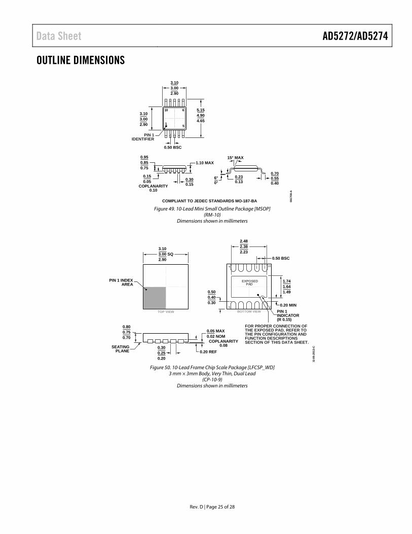
OUTLINE DIMENSIONS
COMPLIANT TO JEDEC STANDARDS MO-187-BA 0917
09-A
6°0°
0.700.550.40
5
10
1
6
0.50 BSC
0.300.15
1.10 MAX
3.103.002.90
COPLANARITY0.10
0.230.13
3.103.002.90
5.154.904.65
PIN 1IDENTIFIER
15° MAX0.950.850.75
0.150.05
Figure 49. 10-Lead Mini Small Outline Package [MSOP]
(RM-10) Dimensions shown in millimeters
2.482.382.23
0.500.400.30
10
1
6
5
0.300.250.20
PIN 1 INDEXAREA
SEATINGPLANE
0.800.750.70
1.741.641.49
0.20 REF
0.05 MAX0.02 NOM
0.50 BSC
EXPOSEDPAD
3.103.00 SQ2.90
PIN 1INDICATOR(R 0.15)
FOR PROPER CONNECTION OFTHE EXPOSED PAD, REFER TOTHE PIN CONFIGURATION ANDFUNCTION DESCRIPTIONSSECTION OF THIS DATA SHEET.COPLANARITY
0.08
02-0
5-20
13-C
TOP VIEW BOTTOM VIEW
0.20 MIN
Figure 50. 10-Lead Frame Chip Scale Package [LFCSP_WD]
3 mm × 3mm Body, Very Thin, Dual Lead (CP-10-9)
Dimensions shown in millimeters

AD5272/AD5274 Data Sheet
Rev. D | Page 26 of 28
ORDERING GUIDE Model1 RAW (kΩ) Resolution Temperature Range Package Description Package Option Branding AD5272BRMZ-20 20 1,024 −40°C to +125°C 10-Lead MSOP RM-10 DE6 AD5272BRMZ-20-RL7 20 1,024 −40°C to +125°C 10-Lead MSOP RM-10 DE6 AD5272BRMZ-50 50 1,024 −40°C to +125°C 10-Lead MSOP RM-10 DE7 AD5272BRMZ-50-RL7 50 1,024 −40°C to +125°C 10-Lead MSOP RM-10 DE7 AD5272BRMZ-100 100 1,024 −40°C to +125°C 10-Lead MSOP RM-10 DE5 AD5272BRMZ-100-RL7 100 1,024 −40°C to +125°C 10-Lead MSOP RM-10 DE5 AD5272BCPZ-20-RL7 20 1,024 −40°C to +125°C 10-Lead LFCSP_WD CP-10-9 DE4 AD5272BCPZ-100-RL7 100 1,024 −40°C to +125°C 10-Lead LFCSP_WD CP-10-9 DE3 AD5274BRMZ-20 20 256 −40°C to +125°C 10-Lead MSOP RM-10 DEE AD5274BRMZ-20-RL7 20 256 −40°C to +125°C 10-Lead MSOP RM-10 DEE AD5274BRMZ-100 100 256 −40°C to +125°C 10-Lead MSOP RM-10 DED AD5274BRMZ-100-RL7 100 256 −40°C to +125°C 10-Lead MSOP RM-10 DED AD5274BCPZ-20-RL7 20 256 −40°C to +125°C 10-Lead LFCSP_WD CP-10-9 DE9 AD5274BCPZ-100-RL7 100 256 −40°C to +125°C 10-Lead LFCSP_WD CP-10-9 DE8 EVAL-AD5272SDZ Evaluation Board 1 Z = RoHS Compliant Part.

Data Sheet AD5272/AD5274
Rev. D | Page 27 of 28
NOTES

AD5272/AD5274 Data Sheet
Rev. D | Page 28 of 28
NOTES
I2C refers to a communications protocol originally developed by Philips Semiconductors (now NXP Semiconductors).
©2009–2013 Analog Devices, Inc. All rights reserved. Trademarks and registered trademarks are the property of their respective owners. D08076-0-3/13(D)
Related Documents